WO2019082343A1 - Dispositif semi-conducteur - Google Patents
Dispositif semi-conducteurInfo
- Publication number
- WO2019082343A1 WO2019082343A1 PCT/JP2017/038755 JP2017038755W WO2019082343A1 WO 2019082343 A1 WO2019082343 A1 WO 2019082343A1 JP 2017038755 W JP2017038755 W JP 2017038755W WO 2019082343 A1 WO2019082343 A1 WO 2019082343A1
- Authority
- WO
- WIPO (PCT)
- Prior art keywords
- lead frame
- semiconductor device
- substrate
- conductive layer
- terminal
- Prior art date
- Legal status (The legal status is an assumption and is not a legal conclusion. Google has not performed a legal analysis and makes no representation as to the accuracy of the status listed.)
- Ceased
Links
Images





Classifications
-
- H—ELECTRICITY
- H10—SEMICONDUCTOR DEVICES; ELECTRIC SOLID-STATE DEVICES NOT OTHERWISE PROVIDED FOR
- H10W—GENERIC PACKAGES, INTERCONNECTIONS, CONNECTORS OR OTHER CONSTRUCTIONAL DETAILS OF DEVICES COVERED BY CLASS H10
- H10W72/00—Interconnections or connectors in packages
-
- H—ELECTRICITY
- H10—SEMICONDUCTOR DEVICES; ELECTRIC SOLID-STATE DEVICES NOT OTHERWISE PROVIDED FOR
- H10W—GENERIC PACKAGES, INTERCONNECTIONS, CONNECTORS OR OTHER CONSTRUCTIONAL DETAILS OF DEVICES COVERED BY CLASS H10
- H10W70/00—Package substrates; Interposers; Redistribution layers [RDL]
- H10W70/40—Leadframes
- H10W70/421—Shapes or dispositions
-
- H—ELECTRICITY
- H10—SEMICONDUCTOR DEVICES; ELECTRIC SOLID-STATE DEVICES NOT OTHERWISE PROVIDED FOR
- H10W—GENERIC PACKAGES, INTERCONNECTIONS, CONNECTORS OR OTHER CONSTRUCTIONAL DETAILS OF DEVICES COVERED BY CLASS H10
- H10W70/00—Package substrates; Interposers; Redistribution layers [RDL]
- H10W70/40—Leadframes
- H10W70/421—Shapes or dispositions
- H10W70/424—Cross-sectional shapes
- H10W70/427—Bent parts
-
- H—ELECTRICITY
- H10—SEMICONDUCTOR DEVICES; ELECTRIC SOLID-STATE DEVICES NOT OTHERWISE PROVIDED FOR
- H10W—GENERIC PACKAGES, INTERCONNECTIONS, CONNECTORS OR OTHER CONSTRUCTIONAL DETAILS OF DEVICES COVERED BY CLASS H10
- H10W70/00—Package substrates; Interposers; Redistribution layers [RDL]
- H10W70/40—Leadframes
- H10W70/464—Additional interconnections in combination with leadframes
- H10W70/466—Tape carriers or flat leads
-
- H—ELECTRICITY
- H10—SEMICONDUCTOR DEVICES; ELECTRIC SOLID-STATE DEVICES NOT OTHERWISE PROVIDED FOR
- H10W—GENERIC PACKAGES, INTERCONNECTIONS, CONNECTORS OR OTHER CONSTRUCTIONAL DETAILS OF DEVICES COVERED BY CLASS H10
- H10W70/00—Package substrates; Interposers; Redistribution layers [RDL]
- H10W70/40—Leadframes
- H10W70/464—Additional interconnections in combination with leadframes
- H10W70/468—Circuit boards
-
- H—ELECTRICITY
- H10—SEMICONDUCTOR DEVICES; ELECTRIC SOLID-STATE DEVICES NOT OTHERWISE PROVIDED FOR
- H10W—GENERIC PACKAGES, INTERCONNECTIONS, CONNECTORS OR OTHER CONSTRUCTIONAL DETAILS OF DEVICES COVERED BY CLASS H10
- H10W70/00—Package substrates; Interposers; Redistribution layers [RDL]
- H10W70/40—Leadframes
- H10W70/481—Leadframes for devices being provided for in groups H10D8/00 - H10D48/00
-
- H—ELECTRICITY
- H10—SEMICONDUCTOR DEVICES; ELECTRIC SOLID-STATE DEVICES NOT OTHERWISE PROVIDED FOR
- H10W—GENERIC PACKAGES, INTERCONNECTIONS, CONNECTORS OR OTHER CONSTRUCTIONAL DETAILS OF DEVICES COVERED BY CLASS H10
- H10W72/00—Interconnections or connectors in packages
- H10W72/60—Strap connectors, e.g. thick copper clips for grounding of power devices
-
- H—ELECTRICITY
- H10—SEMICONDUCTOR DEVICES; ELECTRIC SOLID-STATE DEVICES NOT OTHERWISE PROVIDED FOR
- H10W—GENERIC PACKAGES, INTERCONNECTIONS, CONNECTORS OR OTHER CONSTRUCTIONAL DETAILS OF DEVICES COVERED BY CLASS H10
- H10W74/00—Encapsulations, e.g. protective coatings
- H10W74/10—Encapsulations, e.g. protective coatings characterised by their shape or disposition
- H10W74/111—Encapsulations, e.g. protective coatings characterised by their shape or disposition the semiconductor body being completely enclosed
-
- H—ELECTRICITY
- H10—SEMICONDUCTOR DEVICES; ELECTRIC SOLID-STATE DEVICES NOT OTHERWISE PROVIDED FOR
- H10W—GENERIC PACKAGES, INTERCONNECTIONS, CONNECTORS OR OTHER CONSTRUCTIONAL DETAILS OF DEVICES COVERED BY CLASS H10
- H10W90/00—Package configurations
- H10W90/701—Package configurations characterised by the relative positions of pads or connectors relative to package parts
-
- H—ELECTRICITY
- H10—SEMICONDUCTOR DEVICES; ELECTRIC SOLID-STATE DEVICES NOT OTHERWISE PROVIDED FOR
- H10W—GENERIC PACKAGES, INTERCONNECTIONS, CONNECTORS OR OTHER CONSTRUCTIONAL DETAILS OF DEVICES COVERED BY CLASS H10
- H10W72/00—Interconnections or connectors in packages
- H10W72/01—Manufacture or treatment
- H10W72/016—Manufacture or treatment of strap connectors
- H10W72/01661—Chemical or physical modification, e.g. by sintering or anodisation
-
- H—ELECTRICITY
- H10—SEMICONDUCTOR DEVICES; ELECTRIC SOLID-STATE DEVICES NOT OTHERWISE PROVIDED FOR
- H10W—GENERIC PACKAGES, INTERCONNECTIONS, CONNECTORS OR OTHER CONSTRUCTIONAL DETAILS OF DEVICES COVERED BY CLASS H10
- H10W72/00—Interconnections or connectors in packages
- H10W72/071—Connecting or disconnecting
- H10W72/073—Connecting or disconnecting of die-attach connectors
- H10W72/07351—Connecting or disconnecting of die-attach connectors characterised by changes in properties of the die-attach connectors during connecting
- H10W72/07354—Connecting or disconnecting of die-attach connectors characterised by changes in properties of the die-attach connectors during connecting changes in dispositions
-
- H—ELECTRICITY
- H10—SEMICONDUCTOR DEVICES; ELECTRIC SOLID-STATE DEVICES NOT OTHERWISE PROVIDED FOR
- H10W—GENERIC PACKAGES, INTERCONNECTIONS, CONNECTORS OR OTHER CONSTRUCTIONAL DETAILS OF DEVICES COVERED BY CLASS H10
- H10W72/00—Interconnections or connectors in packages
- H10W72/071—Connecting or disconnecting
- H10W72/076—Connecting or disconnecting of strap connectors
-
- H—ELECTRICITY
- H10—SEMICONDUCTOR DEVICES; ELECTRIC SOLID-STATE DEVICES NOT OTHERWISE PROVIDED FOR
- H10W—GENERIC PACKAGES, INTERCONNECTIONS, CONNECTORS OR OTHER CONSTRUCTIONAL DETAILS OF DEVICES COVERED BY CLASS H10
- H10W72/00—Interconnections or connectors in packages
- H10W72/071—Connecting or disconnecting
- H10W72/076—Connecting or disconnecting of strap connectors
- H10W72/07651—Connecting or disconnecting of strap connectors characterised by changes in properties of the strap connectors during connecting
-
- H—ELECTRICITY
- H10—SEMICONDUCTOR DEVICES; ELECTRIC SOLID-STATE DEVICES NOT OTHERWISE PROVIDED FOR
- H10W—GENERIC PACKAGES, INTERCONNECTIONS, CONNECTORS OR OTHER CONSTRUCTIONAL DETAILS OF DEVICES COVERED BY CLASS H10
- H10W72/00—Interconnections or connectors in packages
- H10W72/30—Die-attach connectors
- H10W72/341—Dispositions of die-attach connectors, e.g. layouts
- H10W72/347—Dispositions of multiple die-attach connectors
-
- H—ELECTRICITY
- H10—SEMICONDUCTOR DEVICES; ELECTRIC SOLID-STATE DEVICES NOT OTHERWISE PROVIDED FOR
- H10W—GENERIC PACKAGES, INTERCONNECTIONS, CONNECTORS OR OTHER CONSTRUCTIONAL DETAILS OF DEVICES COVERED BY CLASS H10
- H10W72/00—Interconnections or connectors in packages
- H10W72/60—Strap connectors, e.g. thick copper clips for grounding of power devices
- H10W72/621—Structures or relative sizes of strap connectors
-
- H—ELECTRICITY
- H10—SEMICONDUCTOR DEVICES; ELECTRIC SOLID-STATE DEVICES NOT OTHERWISE PROVIDED FOR
- H10W—GENERIC PACKAGES, INTERCONNECTIONS, CONNECTORS OR OTHER CONSTRUCTIONAL DETAILS OF DEVICES COVERED BY CLASS H10
- H10W72/00—Interconnections or connectors in packages
- H10W72/60—Strap connectors, e.g. thick copper clips for grounding of power devices
- H10W72/631—Shapes of strap connectors
-
- H—ELECTRICITY
- H10—SEMICONDUCTOR DEVICES; ELECTRIC SOLID-STATE DEVICES NOT OTHERWISE PROVIDED FOR
- H10W—GENERIC PACKAGES, INTERCONNECTIONS, CONNECTORS OR OTHER CONSTRUCTIONAL DETAILS OF DEVICES COVERED BY CLASS H10
- H10W72/00—Interconnections or connectors in packages
- H10W72/60—Strap connectors, e.g. thick copper clips for grounding of power devices
- H10W72/631—Shapes of strap connectors
- H10W72/634—Cross-sectional shape
-
- H—ELECTRICITY
- H10—SEMICONDUCTOR DEVICES; ELECTRIC SOLID-STATE DEVICES NOT OTHERWISE PROVIDED FOR
- H10W—GENERIC PACKAGES, INTERCONNECTIONS, CONNECTORS OR OTHER CONSTRUCTIONAL DETAILS OF DEVICES COVERED BY CLASS H10
- H10W72/00—Interconnections or connectors in packages
- H10W72/60—Strap connectors, e.g. thick copper clips for grounding of power devices
- H10W72/641—Dispositions of strap connectors
- H10W72/642—Dispositions of strap connectors being orthogonal to a side surface of the chip, e.g. in parallel arrangements
-
- H—ELECTRICITY
- H10—SEMICONDUCTOR DEVICES; ELECTRIC SOLID-STATE DEVICES NOT OTHERWISE PROVIDED FOR
- H10W—GENERIC PACKAGES, INTERCONNECTIONS, CONNECTORS OR OTHER CONSTRUCTIONAL DETAILS OF DEVICES COVERED BY CLASS H10
- H10W72/00—Interconnections or connectors in packages
- H10W72/60—Strap connectors, e.g. thick copper clips for grounding of power devices
- H10W72/641—Dispositions of strap connectors
- H10W72/646—Dispositions of strap connectors the connected ends being on auxiliary connecting means on bond pads, e.g. on a bump connector
-
- H—ELECTRICITY
- H10—SEMICONDUCTOR DEVICES; ELECTRIC SOLID-STATE DEVICES NOT OTHERWISE PROVIDED FOR
- H10W—GENERIC PACKAGES, INTERCONNECTIONS, CONNECTORS OR OTHER CONSTRUCTIONAL DETAILS OF DEVICES COVERED BY CLASS H10
- H10W72/00—Interconnections or connectors in packages
- H10W72/60—Strap connectors, e.g. thick copper clips for grounding of power devices
- H10W72/691—Bond pads specially adapted therefor
-
- H—ELECTRICITY
- H10—SEMICONDUCTOR DEVICES; ELECTRIC SOLID-STATE DEVICES NOT OTHERWISE PROVIDED FOR
- H10W—GENERIC PACKAGES, INTERCONNECTIONS, CONNECTORS OR OTHER CONSTRUCTIONAL DETAILS OF DEVICES COVERED BY CLASS H10
- H10W72/00—Interconnections or connectors in packages
- H10W72/851—Dispositions of multiple connectors or interconnections
- H10W72/853—On the same surface
-
- H—ELECTRICITY
- H10—SEMICONDUCTOR DEVICES; ELECTRIC SOLID-STATE DEVICES NOT OTHERWISE PROVIDED FOR
- H10W—GENERIC PACKAGES, INTERCONNECTIONS, CONNECTORS OR OTHER CONSTRUCTIONAL DETAILS OF DEVICES COVERED BY CLASS H10
- H10W72/00—Interconnections or connectors in packages
- H10W72/851—Dispositions of multiple connectors or interconnections
- H10W72/853—On the same surface
- H10W72/868—Die-attach connectors and strap connectors
-
- H—ELECTRICITY
- H10—SEMICONDUCTOR DEVICES; ELECTRIC SOLID-STATE DEVICES NOT OTHERWISE PROVIDED FOR
- H10W—GENERIC PACKAGES, INTERCONNECTIONS, CONNECTORS OR OTHER CONSTRUCTIONAL DETAILS OF DEVICES COVERED BY CLASS H10
- H10W72/00—Interconnections or connectors in packages
- H10W72/851—Dispositions of multiple connectors or interconnections
- H10W72/874—On different surfaces
- H10W72/886—Die-attach connectors and strap connectors
-
- H—ELECTRICITY
- H10—SEMICONDUCTOR DEVICES; ELECTRIC SOLID-STATE DEVICES NOT OTHERWISE PROVIDED FOR
- H10W—GENERIC PACKAGES, INTERCONNECTIONS, CONNECTORS OR OTHER CONSTRUCTIONAL DETAILS OF DEVICES COVERED BY CLASS H10
- H10W72/00—Interconnections or connectors in packages
- H10W72/90—Bond pads, in general
- H10W72/921—Structures or relative sizes of bond pads
- H10W72/926—Multiple bond pads having different sizes
-
- H—ELECTRICITY
- H10—SEMICONDUCTOR DEVICES; ELECTRIC SOLID-STATE DEVICES NOT OTHERWISE PROVIDED FOR
- H10W—GENERIC PACKAGES, INTERCONNECTIONS, CONNECTORS OR OTHER CONSTRUCTIONAL DETAILS OF DEVICES COVERED BY CLASS H10
- H10W90/00—Package configurations
- H10W90/701—Package configurations characterised by the relative positions of pads or connectors relative to package parts
- H10W90/731—Package configurations characterised by the relative positions of pads or connectors relative to package parts of die-attach connectors
- H10W90/736—Package configurations characterised by the relative positions of pads or connectors relative to package parts of die-attach connectors between a chip and a stacked lead frame, conducting package substrate or heat sink
-
- H—ELECTRICITY
- H10—SEMICONDUCTOR DEVICES; ELECTRIC SOLID-STATE DEVICES NOT OTHERWISE PROVIDED FOR
- H10W—GENERIC PACKAGES, INTERCONNECTIONS, CONNECTORS OR OTHER CONSTRUCTIONAL DETAILS OF DEVICES COVERED BY CLASS H10
- H10W90/00—Package configurations
- H10W90/701—Package configurations characterised by the relative positions of pads or connectors relative to package parts
- H10W90/761—Package configurations characterised by the relative positions of pads or connectors relative to package parts of strap connectors
- H10W90/766—Package configurations characterised by the relative positions of pads or connectors relative to package parts of strap connectors between a chip and a stacked lead frame, conducting package substrate or heat sink
Definitions
- the present invention relates to a semiconductor device.
- a semiconductor element is mounted on a conductor layer of a substrate, the semiconductor element and the lead frame are joined by a connector via a conductive bonding material such as solder, and the semiconductor element and the substrate are sealed.
- a semiconductor device sealed with a resin is known (see, for example, Patent Document 1).
- the present invention when stress is applied to the lead frame, the stress generated at the joint portion between the lead frame and the substrate is alleviated, and the reduction in the reliability of the electrical connection of the joint portion is suppressed. It is an object of the present invention to provide a semiconductor device capable of
- a semiconductor device is: A substrate provided with a plurality of conductive layers on the top surface, A semiconductor element disposed on the upper surface of the substrate, the first terminal on the lower surface side being electrically connected to a first conductive layer provided on the upper surface of the substrate; A sealing portion for sealing the substrate and the semiconductor element; A first end is in contact with the upper surface of the first conductive layer at an end extending in the side direction of the upper surface of the substrate in the sealing portion, and the other end is exposed from the sealing portion.
- Lead frame with A first conductive bonding material having conductivity and joining between the upper surface of the first conductive layer and the lower surface side of the one end of the first lead frame at the end of the substrate; Equipped The one end portion of the first lead frame is connected to a first arch portion provided to project upward along the reference direction, and connected to the first arch portion and is more than the first arch portion And a first bent portion that is located on the distal end side and is bent to project downward along the reference direction.
- the lower surface side of the first bent portion is in line contact with the upper surface of the first conductive layer along the reference direction.
- the first conductive bonding material is disposed along the reference direction in which the first bent portion of the first lead frame is in line contact with the top surface of the first conductive layer, and the end of the substrate is The upper surface of the first conductive layer and the lower surface side of the first bent portion are joined in a portion.
- notched portions recessed in the reference direction are formed. Yes, A portion of the first conductive bonding material is embedded in the notch to join between the upper surface of the first conductive layer and the notch of the first bent portion. It is characterized by
- the first lead frame is The side direction in which the end portion of the substrate extends and the reference direction in which a region in line contact with the first bent portion extends are parallel to each other.
- the first lead frame has a main body portion located between the one end portion and the other end portion and sealed in the sealing portion, and the position of the upper surface of the first arch portion is It is characterized in that it is higher than the position of the upper surface of the main body.
- the width in the side direction of the first arch portion is the same as the width in the side direction of the first bent portion other than the notch portion.
- the one end and the other end of the first lead frame have the same thickness.
- the first conductive bonding material is a solder material.
- the first arch portion is Stress applied to the first lead frame is released to the surrounding sealing portion to suppress application of stress to the first bent portion of the first lead frame.
- the position of the lower surface of the first bent portion may be lower than the position of the lower surface of the main body portion.
- a second lead frame in which one end portion is in contact with the upper surface of a second conductive layer provided at the end portion of the upper surface of the substrate in the sealing portion, and the other end portion is exposed from the sealing portion; , A second conductive bonding material having conductivity and joining between the first conductive layer and the one end of the second lead frame at the end of the substrate; And a connector X electrically connecting the second conductive layer and the second terminal on the upper surface side of the semiconductor element,
- the one end of the second lead frame is: A second arch portion provided to project upward along the reference direction; And a second bent portion connected to the second arch portion, located on the tip end side of the second arch portion, and bent downward along the reference direction; The lower side of the second bent portion is in line contact with the upper surface of the second conductive layer along the reference direction.
- the semiconductor device is The first terminal is a drain terminal, the second terminal is a gate terminal, and the source terminal, which is a third terminal having a larger area than the second terminal, is provided on the top surface. It is characterized by
- the width in the reference direction of the one end of the first lead frame is larger than the width in the reference direction of the one end of the second lead frame.
- the semiconductor device may further include a third lead frame whose one end is electrically connected to the third terminal in the sealing portion and whose other end is exposed from the sealing portion.
- a semiconductor device includes a substrate provided with a plurality of conductive layers on an upper surface, and a first conductive disposed on the upper surface of the substrate and having a first terminal on the lower surface provided on the upper surface of the substrate
- the semiconductor element electrically connected to the layer, the sealing portion sealing the substrate and the semiconductor element, and the first conductive layer at an end portion of the one end portion extending in the side direction of the upper surface of the substrate in the sealing portion
- a first lead frame whose other end is exposed from the sealing portion, and the upper surface of the first conductive layer at the end of the substrate and the lower surface side of one end of the first lead frame And a first conductive bonding material having conductivity.
- one end of the first lead frame is connected to the first arch portion provided to project upward along the reference direction, the first arch portion, and the tip end side of the first arch portion And the first bent portion bent to project downward along the reference direction, and the lower surface side of the first bent portion is a line in the reference direction with the upper surface of the first conductive layer It is in contact.
- notched portions recessed in the reference direction are formed.
- a portion of the first conductive bonding material is embedded in the notch to bond between the top surface of the first conductive layer and the notch of the first bent portion.
- the stress applied to the first lead frame L1 is surrounded by the first arch portion provided in the first lead frame. It is possible to escape to the sealing portion of the
- the first bent portion at the tip of the first lead frame is in line contact with the substrate, it is possible to secure the thickness of the conductive bonding material (solder material) around the contact portion.
- notches are formed on both sides of the first bent portion to facilitate bending of the first bent portion, and the solder flows into the notched portion, thereby fixing by the conductive bonding material. Can be assured.
- the stress generated at the joint portion between the lead frame and the substrate can be relaxed.
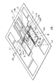
- FIG. 1 is a perspective view showing an example of the configuration of the semiconductor device 100 before sealing.
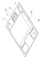
- FIG. 2 is a top view showing an example of the configuration of the semiconductor device 100 before cutting and processing the lead frame after sealing.
- FIG. 3 is a perspective view showing an example of the configuration of the semiconductor device 100 before cutting and processing the lead frame after sealing.
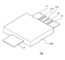
- FIG. 4 is a perspective view showing an example of the configuration of the semiconductor device 100 after cutting and processing the lead frame.
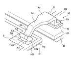
- FIG. 5A is an enlarged perspective view of a region in the vicinity of the first and second lead frames L1 and L2 and the connector X of the semiconductor device 100 shown in FIG.
- FIG. 5B is a perspective view further enlarging the region in the vicinity of the connector X shown in FIG. 5A.
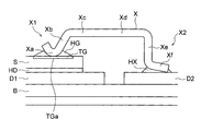
- FIG. 5C is a side view showing an example of the side of the area in the vicinity of the connector X shown in FIG. 5B.
- FIG. 6 is an enlarged perspective view of the area near the first lead frame L1 and the detection lead frame L11 of the semiconductor device 100 shown in FIG.
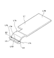
- FIG. 7 is a perspective view showing an example of the configuration of the first lead frame L1 and the first conductive bonding material H1 shown in FIG.
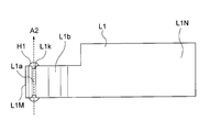
- FIG. 8A is a top view showing an example of the configuration of the first lead frame L1 and the first conductive bonding material H1 shown in FIG.
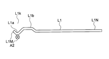
- FIG. 8B is a cross-sectional view showing an example of the configuration of the first lead frame L1 shown in FIG. 8A.
- FIG. 9 is a cross-sectional view showing an example of the configuration in the vicinity of one end portion L1M of the first lead frame L1 shown in FIG.
- FIG. 10 is a view showing an example of steps of a method of manufacturing the semiconductor device 100.
- FIG. 11 is a diagram showing an example of a process of a method of manufacturing the semiconductor device 100 following FIG. 10.
- FIG. 12 is a diagram showing an example of a process of a method of manufacturing the semiconductor device 100 following FIG.
- FIG. 13 is a diagram illustrating an example of a process of the method of manufacturing the semiconductor device 100 following FIG. 12.
- FIG. 1 is a perspective view showing an example of the configuration of the semiconductor device 100 before sealing.
- FIG. 2 is a top view which shows an example of a structure of the semiconductor device 100 before cutting processing of a lead frame after sealing.
- FIG. 3 is a perspective view showing an example of the configuration of the semiconductor device 100 before cutting and processing the lead frame after sealing.
- FIG. 4 is a perspective view showing an example of the configuration of the semiconductor device 100 after cutting and processing the lead frame.
- the case of two first lead frames L1 is shown.
- the example of FIG. 2 is illustrated as the sealing member was permeate
- FIG. 5A is an enlarged perspective view of a region in the vicinity of the first and second lead frames L1 and L2 and the connector X of the semiconductor device 100 shown in FIG.
- FIG. 5B is the perspective view which further expanded the area
- FIG. 5C is a side view which shows an example of the side of the area
- the semiconductor device 100 includes the substrate B, the semiconductor element S, the sealing portion 200, the first lead frame (drain lead frame) L1, and the detection lead frame.
- a conductive joint material for source HS and a lead frame L31 for detection are provided.
- substrate B is provided with the several conductive layer (1st conductive layer D1 and 2nd conductive layer D2) on the upper surface.
- the semiconductor element S is disposed on the upper surface of the substrate B.
- the first terminal TD on the lower surface side is electrically connected to the first conductive layer D1 provided on the upper surface of the substrate B.
- the semiconductor element S includes a first terminal (drain terminal) TD, a second terminal (gate terminal) TG, and a third terminal (source terminal) TS. And.
- the first terminal TD is provided on the lower surface of the semiconductor element S and is electrically connected to the first conductive layer D1.
- the second terminal TG is provided on the top surface of the semiconductor element S, and a control signal (gate signal) is input.
- the semiconductor element S is, for example, a MOSFET.
- the semiconductor element S is provided with a first terminal TD which is a drain terminal on the lower surface, a second terminal TG which is a gate terminal on the upper surface, and a third terminal TS which is a source terminal on the upper surface. Is a MOSFET provided.
- the semiconductor element S may be another semiconductor element such as IGBI other than the MOSFET.
- one end L1M is electrically connected to the first terminal TD which is a drain terminal in the sealing portion 200, and the other end L1N Are exposed from the sealing portion 200.
- one end L1M contacts the upper surface of the first conductive layer D1 at the end extending in the side direction A1 of the upper surface of the substrate B in the sealing portion 200, and the other end The portion L1N is exposed from the sealing portion 200.
- One end L1M of the first lead frame L1 includes a first arch L1b and a first bent L1a.
- the first arch portion L1b is provided to project upward along the reference direction A2.
- the first bent portion L1a is connected to the first arch portion L1b, is positioned on the tip side of the first arch portion L1b, and is bent so as to project downward along the reference direction A2.
- the lower surface side of the first bent portion L1a is in line contact with the upper surface of the first conductive layer D12 along the reference direction A2.
- the first conductive bonding material H1 bonds the upper surface of the first conductive layer D1 to the lower surface side of the one end L1M of the first lead frame L1 at the end of the substrate B and has conductivity. Have.
- the first conductive bonding material H1 is, for example, a solder material.
- the detection lead frame L11 has one end electrically connected to the first terminal TD which is a drain terminal in the sealing portion 200, and the other end is exposed from the sealing portion 200.
- the detection lead frame L11 is for detecting, for example, the voltage of the drain of the semiconductor element S.
- the conductive bonding material for detection H11 bonds between the first conductive layer D1 and one end portion of the lead frame for detection L11 and has conductivity.
- the detection conductive bonding material H11 is, for example, a solder material.
- the second lead frame L2 has the one end L2M on the upper surface of the second conductive layer provided at the end of the upper surface of the substrate B in the sealing portion 200. , And the other end L 2 N is exposed from the sealing portion 200.
- the second lead frame L2 is a control lead frame for transmitting a gate signal of the above-described MOSFET (semiconductor element S).
- the second conductive bonding material (first conductive control bonding material for control) H2 is disposed between the first conductive layer D1 and the one end L2M of the second lead frame L2 at the end of the substrate B. Bonding and having conductivity.
- the second conductive bonding material H2 is, for example, a solder material.
- one end L2M of the second lead frame L2 includes a second arch L2b and a second bent L2a.
- the second arch portion L2b is provided to project upward along the reference direction A2.
- the second bent portion L2a is connected to the second arch portion L2b, is located on the tip side of the second arch portion L2b, and is bent so as to protrude downward along the reference direction A2.
- the lower side of the second bent portion L2a is in line contact with the upper surface of the second conductive layer D2 along the reference direction A2.
- the width in the reference direction A2 of the one end L1M of the first lead frame L1 is set to be larger than the width in the reference direction A2 of the one end L2M of the second lead frame L2.
- one end L3M is electrically connected to the third terminal TS which is a source terminal on the upper surface of the semiconductor element S, and the other end L3N is exposed from the sealing portion 200. .
- the source conductive bonding material HS bonds between the third terminal TS and the one end L3M of the third lead frame L3 and has conductivity.
- the source conductive bonding material HS is, for example, a solder material.
- the detection lead frame L31 has one end electrically connected to the third terminal TS which is the source terminal on the upper surface of the semiconductor element S (ie, extending from the third lead frame L3), and the other end The portion is exposed from the sealing portion 200.
- the detection lead frame L31 is for detecting, for example, the voltage of the source of the semiconductor element S.
- the sealing unit 200 seals the substrate B and the semiconductor element S.
- the area of the source terminal which is the third terminal TS on the top surface of the semiconductor element S is larger than the area of the second terminal TG which is the gate terminal. It is set to become.
- the connector X electrically connects between the second conductive layer D2 and the second terminal (gate terminal) TG on the upper surface side of the semiconductor element S as shown in, for example, FIGS. 5A, 5B, and 5C. Are supposed to be connected.
- this connector X contacts the upper surface of the second terminal TG of the semiconductor element S in the sealing portion 200 at one end X1 and the other end X2 It is in contact with the second conductive layer D.
- the second control conductive bonding material HG bonds between the upper surface of the second terminal TG of the semiconductor element S and the one end portion X1 of the connector X and has conductivity.
- the second control conductive bonding material HG is, for example, a solder material.
- the third control conductive bonding material HX bonds between the second conductive layer D2 of the substrate B and the other end X2 of the connector X and has conductivity.
- the third control conductive bonding material HX is, for example, a solder material.
- the connector X is between the second conductive layer D2 and the second terminal (gate terminal) TG on the upper surface side of the semiconductor element S by the second and third control conductive bonding materials HG and HX. Are connected electrically.
- one end X1 of the connector X includes a horizontal portion Xc, a first inclined portion Xb, a control bending portion Xa, and a reference portion Xd.
- the horizontal part Xc is arrange
- the first inclined portion Xb is connected to the horizontal portion Xc and positioned on the tip end side of the one end portion X1 with respect to the horizontal portion Xc. It has a shape inclined downward from.
- control bending portion Xa is connected to the first inclined portion Xb and located at the tip of the one end portion X1, and protrudes downward along the bending axis direction A3. It is bent.
- the lower surface side of the control bending portion Xa is in contact with the upper surface of the second terminal TG.
- the lower surface side of the control bending portion Xa is in contact with the center TGa of the upper surface of the second terminal TG.
- control bending portion Xa is in line contact with the upper surface of the second terminal TG in the bending axial direction A3, as shown in FIG. 5C, for example.
- the width in the bending axis direction A3 of the control bending portion Xa is the same as the width in the bending axis direction A3 of the first inclined portion Xb.
- the reference portion Xd is connected to the horizontal portion Xc on the opposite side to the first inclined portion Xb and has a width larger than the width of the horizontal portion Xc.
- the width in the bending axis direction A3 of the control bending portion Xa is set to be smaller than the width in the bending axis direction A3 of the reference portion Xd.
- the second control conductive bonding material HG has a control bending portion Xa of the connector X in line contact with the top surface of the second terminal TG. It arrange
- the upper surface of the second terminal TG has, for example, a rectangular shape as shown in FIGS. 5A, 5B, and 5C.
- the second control conductive bonding material HG is positioned so as to surround the center TGa of the upper surface of the second terminal TG as shown in FIG. 5B, and the lower surface of the control bending portion Xa of the connector X And the upper surface of the second terminal TG.
- the bending axis direction A3 is, for example, parallel to one side of the rectangle of the second terminal TG, as shown in FIGS. 5A, 5B, and 5C.
- the other end X2 of the connector X includes a second inclined portion Xe and a tip end Xf.
- the second inclined portion Xe is connected to the reference portion Xd on the side opposite to the horizontal portion Xc, and is positioned on the tip end side of the other end X2 with respect to the reference portion Xd and inclined downward from the reference portion Xd.
- the tip end portion Xf is connected to the second inclined portion Xe and located at the tip end of the other end portion X2.
- the front end portion Xf is bonded to the upper surface of the second conductive layer D2 of the substrate B by the third control conductive bonding material HX.
- the height from the upper surface of the substrate B of the lower surface of the control bent portion Xa of the connector X is set to be higher than the height from the upper surface of the substrate B of the lower surface of the tip portion Xf.
- the thickness in the vertical direction of the connector X is set to be thinner than the thickness in the vertical direction of the second lead frame L2.
- FIG. 6 is an enlarged perspective view of a region in the vicinity of the first lead frame L1 and the detection lead frame L11 of the semiconductor device 100 shown in FIG. 7 is a perspective view showing an example of the configuration of the first lead frame L1 and the first conductive bonding material H1 shown in FIG.
- FIG. 8A is a top view showing an example of the configuration of the first lead frame L1 and the first conductive bonding material H1 shown in FIG. 8B is a cross-sectional view showing an example of the configuration of the first lead frame L1 shown in FIG. 8A.
- 9 is a cross-sectional view showing an example of the configuration in the vicinity of one end portion L1M of the first lead frame L1 shown in FIG.
- one end L1M of the first lead frame L1 includes a first arch L1b and a first bent L1a.
- the first arch portion L1b is provided to project upward along the reference direction A2.
- the first bent portion L1a is connected to the first arch portion L1b, is positioned on the tip side of the first arch portion L1b, and is bent so as to project downward along the reference direction A2.
- the lower surface side of the first bent portion L1a of the first lead frame L1 is in line contact with the upper surface of the first conductive layer D12 along the reference direction A2.
- the first conductive bonding material H1 is disposed along the reference direction A2 in which the first bent portion L1a of the first lead frame L1 is in line contact with the upper surface of the first conductive layer D1.
- the first conductive bonding material H1 bonds the upper surface of the first conductive layer D1 to the lower surface side of the first bent portion L1a at the end of the substrate B.
- the side surfaces on both sides of the reference direction A2 of the portion of the first bent portion L1a of the first lead frame L1 in line contact with the first conductive layer D1 are A notch L1k recessed in the reference direction A2 is formed.
- a portion of the first conductive bonding material H1 is embedded in the notch portion L1k, and joins between the upper surface of the first conductive layer D1 and the notch portion L1k of the first bent portion L1a. doing.
- the side direction A1 where the end of the substrate B extends and the region where the first bent portion L1a makes line contact is extended It is arranged to be parallel to the existing reference direction A2.
- first lead frame L1 has a main body portion located between the one end portion L1M and the other end portion L1N and sealed in the sealing portion 200, and the first lead frame L1 has an upper surface of the first arch portion L1b. The position is higher than the position of the upper surface of the main body.
- the width in the side direction A1 of the first arch portion L1b is the same as the width in the side direction A1 other than the notch L1k of the first bent portion L1a. That is, the width in the side direction A1 of the first arch portion L1b is larger than the width in the side direction A1 of the notch L1k of the first bent portion L1a.
- one end L1M and the other end L1N of the first lead frame L1 have the same thickness (that is, the first lead frame L1 is not coined).
- the position of the lower surface of the first bent portion L1a is set to be lower than the position of the lower surface of the main body.
- the first arch portion L1b releases the stress applied to the first lead frame L1 to the peripheral sealing portion 200, and the stress is applied to the first bent portion L1a of the first lead frame L1. It is supposed to suppress being done.
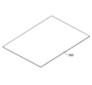
- FIGS. 10 to 13 illustrate an example of steps of a method of manufacturing the semiconductor device 100.
- FIGS. 10 to 13 illustrate an example of steps of a method of manufacturing the semiconductor device 100.
- a metal plate 300 made of a metal such as copper is prepared.
- portions to be the first to third lead frames L1 to L3 are simultaneously formed.
- the notch part L1k indented in the reference direction A2 is formed in the side of the both sides of.
- the notch part L2k which dented in the reference direction A2 is formed in the side of the both sides of.
- the first and second bent portions L1a are bent by bending one end of the first and second lead frames L1 and L2 so as to protrude downward along the reference direction A2. , L2a.
- the third lead frame L3 is subjected to predetermined processing to form a predetermined shape L3X.
- first to third lead frames L1 to L3 shown in FIG. 1 are formed.
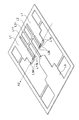
- the substrate B provided with the first conductive layer D1 and the second conductive layer D2 on the top surface is prepared.
- a semiconductor element having a first terminal TD provided on the lower surface and electrically connected to the first conductive layer D1, and a second terminal TG provided on the upper surface and receiving the control signal. S is disposed on the top surface of the substrate B. Then, the first terminal TD is joined to the first conductive layer D1 to electrically connect the first conductive layer D1 and the first terminal TD.
- one end of the first lead frame L1 is brought into contact with the upper surface of the first conductive layer D1 provided at the end of the upper surface of the substrate B.
- the first conductive bonding material H1 joins the upper surface of the first conductive layer to the lower surface side of the first bent portion of the first lead frame L1 at the end of the substrate B, and A part of the first conductive bonding material H1 is embedded in the notch L1k, and the upper surface of the first conductive layer D1 and the notch L1k of the first bent portion L1a are joined.
- one end of the second lead frame L2 is brought into contact with the upper surface of the second conductive layer D2 provided at the end of the upper surface of the substrate B. Then, between the second conductive layer D2 and one end of the second lead frame L2 are joined at the end of the substrate B by the first conductive control bonding material H2 having conductivity (FIG. 1) . At this time, a part of the second conductive bonding material H2 is embedded in the notch portion L2k, and the upper surface of the second conductive layer D2 and the notch portion L2k of the second bent portion L2a are joined. .
- one end of the third lead frame L3 is brought into contact with the upper surface of the third terminal TS on the upper surface of the semiconductor element S. Then, the third terminal TS and one end portion of the third lead frame L3 are joined by the conductive conductive bonding material for source HS having conductivity (FIG. 1).
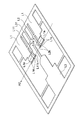
- the second control conductive bonding material HG bonds the top surface of the second terminal of the semiconductor element S to the one end X1 of the connector X, and also has a third conductive control property having conductivity.
- the second conductive layer D2 of the substrate B and the other end X2 of the connector X are bonded by the bonding material HX.
- the sealing portion 200 is used to form the substrate B, the semiconductor element S, the connector X, the first to third lead frames L1 to L3, and the detection lead frames L11 and L31. Seal one end of the
- the first to third lead frames L1 to L3 and the detection lead frames L11 and L31 are cut and processed, whereby the semiconductor device 100 shown in FIG. 4 is manufactured.
- the first and second lead frames L1 and L2 are bent in two steps by bending one end of the first and second lead frames L1 and L2. , L2 can be formed. For this reason, the processing cost is reduced, and stress relaxation is possible because the solder thickness is secured on the outer peripheral portion of the joint.
- notches (recesses) L1k and L2k are formed on both sides of the first and second bent portions L1a and L2a of the tip (one end) of the first and second lead frames L1 and L2, respectively, Fixing by the solder can be ensured by the solder flowing into the notched portions L1k, L2k while facilitating bending of the first and second bent portions L1a, L2a.
- the bent first and second bent portions L1a and L2a are in line contact with each other. Because it is connected to the first and second conductive layers D1 and D2, the amount of dispensing of the solder material can be reduced.
- the substrate B provided with the plurality of conductive layers D1 and D2 on the upper surface, the first terminal disposed on the upper surface of the substrate and the lower surface is the substrate A semiconductor element S electrically connected to the first conductive layer D1 provided on the upper surface, a sealing portion for sealing the substrate and the semiconductor element, and a side direction A1 of one surface of the upper surface of the substrate in the sealing portion
- the first lead frame L1 is in contact with the upper surface of the first conductive layer at the end extending to the top and the other end is exposed from the sealing portion, and the upper surface of the first conductive layer at the end of the substrate And a lower surface side of one end portion of the first lead frame, and has a conductive first conductive bonding material H1.
- one end portion of the first lead frame is connected to the first arch portion L1 b provided to project upward along the reference direction A2, and to the first arch portion, and is more than the first arch portion
- a first bent portion L1a which is located on the tip end side and bent to project downward along the reference direction, and the lower surface side of the first bent portion is the upper surface of the first conductive layer and the reference Line contact in the direction.
- the first bent portion L1a at the end of the first lead frame is in line contact with the substrate B, it is possible to secure the thickness of the conductive bonding material (solder material) around the contact portion. Become.
- notches L1k are formed on both sides of the first bent portion L1a, and the solder flows into the notched portion L1K while facilitating the bending of the first bent portion L1a. Fixing by the bonding material can be ensured.
- the stress generated at the joint portion between the lead frame and the substrate can be relaxed.
Landscapes
- Lead Frames For Integrated Circuits (AREA)
Abstract
La présente invention concerne un dispositif semi-conducteur qui comporte : un substrat qui a une pluralité de couches conductrices disposées sur sa surface supérieure ; un élément semi-conducteur qui est disposé sur la surface supérieure du substrat et qui a, du côté de la surface inférieure, une première borne afin d'être connecté électriquement à une première couche conductrice disposée sur la surface supérieure du substrat ; une partie étanche qui scelle le substrat et l'élément semi-conducteur ; une première grille de connexion dont une extrémité est en contact avec la surface supérieure de la première couche conductrice à une section d'extrémité, sur la surface supérieure, du substrat, la section d'extrémité s'étendant le long de la direction du bord dans la partie étanche, et dont l'autre extrémité est découverte depuis la partie étanche ; et un premier matériau conducteur de jonction qui a une conductivité et qui joint, à la section d'extrémité du substrat, la surface supérieure de la première couche conductrice et le côté de la surface inférieure de ladite extrémité de la première grille de connexion, ladite extrémité de la première grille de connexion ayant une première partie en arche qui est réalisée de manière à se projeter vers le haut le long d'une direction de référence, et une première partie courbée qui est connectée à la première partie en arche, qui est positionnée plus loin vers le côté de l'extrémité avant que la première partie en arche, et qui est courbée de manière à se projeter vers le bas le long de la direction de référence.
Priority Applications (6)
| Application Number | Priority Date | Filing Date | Title |
|---|---|---|---|
| CN201780093212.0A CN111316429A (zh) | 2017-10-26 | 2017-10-26 | 半导体装置 |
| JP2019549779A JP6752980B2 (ja) | 2017-10-26 | 2017-10-26 | 半導体装置 |
| EP17929433.5A EP3703118B1 (fr) | 2017-10-26 | 2017-10-26 | Dispositif semi-conducteur |
| PCT/JP2017/038755 WO2019082343A1 (fr) | 2017-10-26 | 2017-10-26 | Dispositif semi-conducteur |
| CN202510498928.5A CN120376535A (zh) | 2017-10-26 | 2017-10-26 | 半导体装置 |
| US16/630,690 US11309232B2 (en) | 2017-10-26 | 2017-10-26 | Semiconductor device |
Applications Claiming Priority (1)
| Application Number | Priority Date | Filing Date | Title |
|---|---|---|---|
| PCT/JP2017/038755 WO2019082343A1 (fr) | 2017-10-26 | 2017-10-26 | Dispositif semi-conducteur |
Publications (1)
| Publication Number | Publication Date |
|---|---|
| WO2019082343A1 true WO2019082343A1 (fr) | 2019-05-02 |
Family
ID=66246292
Family Applications (1)
| Application Number | Title | Priority Date | Filing Date |
|---|---|---|---|
| PCT/JP2017/038755 Ceased WO2019082343A1 (fr) | 2017-10-26 | 2017-10-26 | Dispositif semi-conducteur |
Country Status (5)
| Country | Link |
|---|---|
| US (1) | US11309232B2 (fr) |
| EP (1) | EP3703118B1 (fr) |
| JP (1) | JP6752980B2 (fr) |
| CN (2) | CN111316429A (fr) |
| WO (1) | WO2019082343A1 (fr) |
Cited By (2)
| Publication number | Priority date | Publication date | Assignee | Title |
|---|---|---|---|---|
| CN115621237A (zh) * | 2021-07-12 | 2023-01-17 | 新电元工业株式会社 | 端子部件以及半导体装置 |
| JP2025119582A (ja) * | 2024-02-01 | 2025-08-14 | リテルフューズ、インコーポレイテッド | 半導体デバイスパッケージ内のメタルコネクタ |
Citations (8)
| Publication number | Priority date | Publication date | Assignee | Title |
|---|---|---|---|---|
| JPH01100957A (ja) * | 1987-10-14 | 1989-04-19 | Nippon Denso Co Ltd | ハイブリッドic |
| JPH06181276A (ja) * | 1992-12-15 | 1994-06-28 | Shinko Electric Ind Co Ltd | 半導体装置用リード |
| JP2002299541A (ja) * | 2001-03-28 | 2002-10-11 | Densei Lambda Kk | 表面実装用電源装置におけるリード |
| JP2009049272A (ja) * | 2007-08-22 | 2009-03-05 | Mitsubishi Electric Corp | 半導体装置およびその製造方法 |
| JP2015012065A (ja) | 2013-06-27 | 2015-01-19 | 株式会社デンソー | 半導体装置の製造方法 |
| JP2015090965A (ja) * | 2013-11-07 | 2015-05-11 | 三菱電機株式会社 | 半導体装置 |
| WO2016084483A1 (fr) * | 2014-11-27 | 2016-06-02 | 新電元工業株式会社 | Grille de connexion, dispositif à semi-conducteur, procédé de fabrication de grille de connexion et procédé de fabrication de dispositif à semi-conducteur |
| JP2017174927A (ja) * | 2016-03-23 | 2017-09-28 | 三菱マテリアル株式会社 | パワーモジュール及びその製造方法 |
Family Cites Families (11)
| Publication number | Priority date | Publication date | Assignee | Title |
|---|---|---|---|---|
| JPS576251U (fr) * | 1980-06-11 | 1982-01-13 | ||
| US5001545A (en) * | 1988-09-09 | 1991-03-19 | Motorola, Inc. | Formed top contact for non-flat semiconductor devices |
| JP2000049184A (ja) * | 1998-05-27 | 2000-02-18 | Hitachi Ltd | 半導体装置およびその製造方法 |
| JP3767398B2 (ja) * | 2001-03-19 | 2006-04-19 | カシオ計算機株式会社 | 半導体装置およびその製造方法 |
| CN100418216C (zh) * | 2004-11-30 | 2008-09-10 | 株式会社东芝 | 半导体封装及半导体模块 |
| JP5252819B2 (ja) * | 2007-03-26 | 2013-07-31 | 三菱電機株式会社 | 半導体装置およびその製造方法 |
| JP2011023517A (ja) * | 2009-07-15 | 2011-02-03 | Hitachi Cable Ltd | 半導体装置用tabテープおよびその製造方法 |
| WO2012120568A1 (fr) * | 2011-03-09 | 2012-09-13 | パナソニック株式会社 | Dispositif semiconducteur |
| JP6363825B2 (ja) | 2013-07-29 | 2018-07-25 | 新電元工業株式会社 | 半導体装置及びリードフレーム |
| JP6201626B2 (ja) * | 2013-10-23 | 2017-09-27 | スミダコーポレーション株式会社 | 電子部品及び電子部品の製造方法 |
| JP2015095474A (ja) * | 2013-11-08 | 2015-05-18 | アイシン精機株式会社 | 電子部品パッケージ |
-
2017
- 2017-10-26 WO PCT/JP2017/038755 patent/WO2019082343A1/fr not_active Ceased
- 2017-10-26 CN CN201780093212.0A patent/CN111316429A/zh active Pending
- 2017-10-26 JP JP2019549779A patent/JP6752980B2/ja active Active
- 2017-10-26 CN CN202510498928.5A patent/CN120376535A/zh active Pending
- 2017-10-26 US US16/630,690 patent/US11309232B2/en active Active
- 2017-10-26 EP EP17929433.5A patent/EP3703118B1/fr active Active
Patent Citations (8)
| Publication number | Priority date | Publication date | Assignee | Title |
|---|---|---|---|---|
| JPH01100957A (ja) * | 1987-10-14 | 1989-04-19 | Nippon Denso Co Ltd | ハイブリッドic |
| JPH06181276A (ja) * | 1992-12-15 | 1994-06-28 | Shinko Electric Ind Co Ltd | 半導体装置用リード |
| JP2002299541A (ja) * | 2001-03-28 | 2002-10-11 | Densei Lambda Kk | 表面実装用電源装置におけるリード |
| JP2009049272A (ja) * | 2007-08-22 | 2009-03-05 | Mitsubishi Electric Corp | 半導体装置およびその製造方法 |
| JP2015012065A (ja) | 2013-06-27 | 2015-01-19 | 株式会社デンソー | 半導体装置の製造方法 |
| JP2015090965A (ja) * | 2013-11-07 | 2015-05-11 | 三菱電機株式会社 | 半導体装置 |
| WO2016084483A1 (fr) * | 2014-11-27 | 2016-06-02 | 新電元工業株式会社 | Grille de connexion, dispositif à semi-conducteur, procédé de fabrication de grille de connexion et procédé de fabrication de dispositif à semi-conducteur |
| JP2017174927A (ja) * | 2016-03-23 | 2017-09-28 | 三菱マテリアル株式会社 | パワーモジュール及びその製造方法 |
Cited By (2)
| Publication number | Priority date | Publication date | Assignee | Title |
|---|---|---|---|---|
| CN115621237A (zh) * | 2021-07-12 | 2023-01-17 | 新电元工业株式会社 | 端子部件以及半导体装置 |
| JP2025119582A (ja) * | 2024-02-01 | 2025-08-14 | リテルフューズ、インコーポレイテッド | 半導体デバイスパッケージ内のメタルコネクタ |
Also Published As
| Publication number | Publication date |
|---|---|
| CN111316429A (zh) | 2020-06-19 |
| EP3703118B1 (fr) | 2022-05-18 |
| JPWO2019082343A1 (ja) | 2020-04-16 |
| CN120376535A (zh) | 2025-07-25 |
| JP6752980B2 (ja) | 2020-09-09 |
| EP3703118A4 (fr) | 2020-09-02 |
| US11309232B2 (en) | 2022-04-19 |
| US20200395276A1 (en) | 2020-12-17 |
| EP3703118A1 (fr) | 2020-09-02 |
Similar Documents
| Publication | Publication Date | Title |
|---|---|---|
| CN102725844B (zh) | 导电通路、使用该导电通路的半导体装置以及它们的制造方法 | |
| EP2930747A1 (fr) | Conducteur destiné à être connecté à un dispositif à semi-conducteur | |
| US20180049316A1 (en) | Circuit structure | |
| JP6752981B2 (ja) | 半導体装置の製造方法 | |
| WO2019082343A1 (fr) | Dispositif semi-conducteur | |
| KR20180045842A (ko) | 칩 패키징 구조 및 관련된 인너 리드 본딩 방법 | |
| KR101644913B1 (ko) | 초음파 용접을 이용한 반도체 패키지 및 제조 방법 | |
| JP6080305B2 (ja) | 半導体装置の製造方法、半導体装置及びリードフレーム | |
| JP6466625B1 (ja) | 半導体装置 | |
| JP6752982B2 (ja) | 半導体装置、及び、半導体装置の製造方法 | |
| JP6808849B2 (ja) | 半導体装置 | |
| JP2012238749A (ja) | 半導体装置 | |
| JP2024027893A (ja) | 半導体装置 |
Legal Events
| Date | Code | Title | Description |
|---|---|---|---|
| 121 | Ep: the epo has been informed by wipo that ep was designated in this application |
Ref document number: 17929433 Country of ref document: EP Kind code of ref document: A1 |
|
| ENP | Entry into the national phase |
Ref document number: 2019549779 Country of ref document: JP Kind code of ref document: A |
|
| NENP | Non-entry into the national phase |
Ref country code: DE |
|
| ENP | Entry into the national phase |
Ref document number: 2017929433 Country of ref document: EP Effective date: 20200526 |