WO2019082929A1 - フィルムコンデンサ、連結型コンデンサと、これを用いたインバータおよび電動車輌 - Google Patents
フィルムコンデンサ、連結型コンデンサと、これを用いたインバータおよび電動車輌Info
- Publication number
- WO2019082929A1 WO2019082929A1 PCT/JP2018/039498 JP2018039498W WO2019082929A1 WO 2019082929 A1 WO2019082929 A1 WO 2019082929A1 JP 2018039498 W JP2018039498 W JP 2018039498W WO 2019082929 A1 WO2019082929 A1 WO 2019082929A1
- Authority
- WO
- WIPO (PCT)
- Prior art keywords
- film
- metal film
- groove
- metal
- metallized
- Prior art date
- Legal status (The legal status is an assumption and is not a legal conclusion. Google has not performed a legal analysis and makes no representation as to the accuracy of the status listed.)
- Ceased
Links
Images


Classifications
-
- H—ELECTRICITY
- H01—ELECTRIC ELEMENTS
- H01G—CAPACITORS; CAPACITORS, RECTIFIERS, DETECTORS, SWITCHING DEVICES, LIGHT-SENSITIVE OR TEMPERATURE-SENSITIVE DEVICES OF THE ELECTROLYTIC TYPE
- H01G4/00—Fixed capacitors; Processes of their manufacture
- H01G4/33—Thin- or thick-film capacitors (thin- or thick-film circuits; capacitors without a potential-jump or surface barrier specially adapted for integrated circuits, details thereof, multistep manufacturing processes therefor)
-
- H—ELECTRICITY
- H01—ELECTRIC ELEMENTS
- H01G—CAPACITORS; CAPACITORS, RECTIFIERS, DETECTORS, SWITCHING DEVICES, LIGHT-SENSITIVE OR TEMPERATURE-SENSITIVE DEVICES OF THE ELECTROLYTIC TYPE
- H01G4/00—Fixed capacitors; Processes of their manufacture
- H01G4/002—Details
- H01G4/005—Electrodes
- H01G4/015—Special provisions for self-healing
-
- H—ELECTRICITY
- H01—ELECTRIC ELEMENTS
- H01G—CAPACITORS; CAPACITORS, RECTIFIERS, DETECTORS, SWITCHING DEVICES, LIGHT-SENSITIVE OR TEMPERATURE-SENSITIVE DEVICES OF THE ELECTROLYTIC TYPE
- H01G4/00—Fixed capacitors; Processes of their manufacture
- H01G4/002—Details
- H01G4/005—Electrodes
- H01G4/012—Form of non-self-supporting electrodes
-
- H—ELECTRICITY
- H01—ELECTRIC ELEMENTS
- H01G—CAPACITORS; CAPACITORS, RECTIFIERS, DETECTORS, SWITCHING DEVICES, LIGHT-SENSITIVE OR TEMPERATURE-SENSITIVE DEVICES OF THE ELECTROLYTIC TYPE
- H01G4/00—Fixed capacitors; Processes of their manufacture
- H01G4/002—Details
- H01G4/228—Terminals
-
- H—ELECTRICITY
- H01—ELECTRIC ELEMENTS
- H01G—CAPACITORS; CAPACITORS, RECTIFIERS, DETECTORS, SWITCHING DEVICES, LIGHT-SENSITIVE OR TEMPERATURE-SENSITIVE DEVICES OF THE ELECTROLYTIC TYPE
- H01G4/00—Fixed capacitors; Processes of their manufacture
- H01G4/32—Wound capacitors
-
- H—ELECTRICITY
- H01—ELECTRIC ELEMENTS
- H01G—CAPACITORS; CAPACITORS, RECTIFIERS, DETECTORS, SWITCHING DEVICES, LIGHT-SENSITIVE OR TEMPERATURE-SENSITIVE DEVICES OF THE ELECTROLYTIC TYPE
- H01G4/00—Fixed capacitors; Processes of their manufacture
- H01G4/38—Multiple capacitors, i.e. structural combinations of fixed capacitors
- H01G4/385—Single unit multiple capacitors, e.g. dual capacitor in one coil
-
- H—ELECTRICITY
- H01—ELECTRIC ELEMENTS
- H01G—CAPACITORS; CAPACITORS, RECTIFIERS, DETECTORS, SWITCHING DEVICES, LIGHT-SENSITIVE OR TEMPERATURE-SENSITIVE DEVICES OF THE ELECTROLYTIC TYPE
- H01G4/00—Fixed capacitors; Processes of their manufacture
- H01G4/40—Structural combinations of fixed capacitors with other electric elements, the structure mainly consisting of a capacitor, e.g. RC combinations
-
- H—ELECTRICITY
- H01—ELECTRIC ELEMENTS
- H01G—CAPACITORS; CAPACITORS, RECTIFIERS, DETECTORS, SWITCHING DEVICES, LIGHT-SENSITIVE OR TEMPERATURE-SENSITIVE DEVICES OF THE ELECTROLYTIC TYPE
- H01G4/00—Fixed capacitors; Processes of their manufacture
- H01G4/002—Details
- H01G4/018—Dielectrics
- H01G4/06—Solid dielectrics
- H01G4/14—Organic dielectrics
- H01G4/18—Organic dielectrics of synthetic material, e.g. derivatives of cellulose
-
- H—ELECTRICITY
- H02—GENERATION; CONVERSION OR DISTRIBUTION OF ELECTRIC POWER
- H02M—APPARATUS FOR CONVERSION BETWEEN AC AND AC, BETWEEN AC AND DC, OR BETWEEN DC AND DC, AND FOR USE WITH MAINS OR SIMILAR POWER SUPPLY SYSTEMS; CONVERSION OF DC OR AC INPUT POWER INTO SURGE OUTPUT POWER; CONTROL OR REGULATION THEREOF
- H02M7/00—Conversion of AC power input into DC power output; Conversion of DC power input into AC power output
- H02M7/003—Constructional details, e.g. physical layout, assembly, wiring or busbar connections
-
- Y—GENERAL TAGGING OF NEW TECHNOLOGICAL DEVELOPMENTS; GENERAL TAGGING OF CROSS-SECTIONAL TECHNOLOGIES SPANNING OVER SEVERAL SECTIONS OF THE IPC; TECHNICAL SUBJECTS COVERED BY FORMER USPC CROSS-REFERENCE ART COLLECTIONS [XRACs] AND DIGESTS
- Y02—TECHNOLOGIES OR APPLICATIONS FOR MITIGATION OR ADAPTATION AGAINST CLIMATE CHANGE
- Y02T—CLIMATE CHANGE MITIGATION TECHNOLOGIES RELATED TO TRANSPORTATION
- Y02T10/00—Road transport of goods or passengers
- Y02T10/60—Other road transportation technologies with climate change mitigation effect
- Y02T10/70—Energy storage systems for electromobility, e.g. batteries
Definitions
- the present disclosure relates to a film capacitor, a coupled capacitor, an inverter using the same, and an electric vehicle.
- the film capacitor has, for example, a dielectric film obtained by filming a polypropylene resin, and a metal film formed on the surface of the dielectric film by vapor deposition.
- a metal film is used as an electrode.
- the film capacitor is unlikely to generate a fire or an electric shock when the electric circuit is short-circuited. Therefore, in recent years, applications of film capacitors are being expanded to power supply circuits such as light emitting diode (LED) lighting, motor drive of hybrid vehicles, inverter systems for solar power generation, and the like.
- LED light emitting diode
- Patent Document 1 discloses a technique for raising the thickness of the metal film at the portion connected to the external electrode.
- the film capacitor of the present disclosure comprises: a first dielectric film; a first metallized film having a first metal film disposed on a first surface of the first dielectric film; a second dielectric film; A second metallized film having a second metal film disposed on a second surface of the second dielectric film, and a main body including at least a pair of external electrodes.
- the first dielectric film or the second dielectric film is disposed between the first metal film and the second metal film.
- the external electrodes are respectively disposed at a pair of main body end portions in the first direction of the main body portion, and are electrically connected to any one of the first metal film and the second metal film.
- the first metal film and / or the second metal film electrically connected to the external electrode may have a thickness of 20 nm or more in the vicinity of the end portion of the main body electrically connected to the external electrode. It has one portion, and the first portion has a plurality of first grooves in contact with the body end and extending in the first direction.
- a and / or B this refers to either "A only", “B only”, or "A and B.”
- the coupled capacitor of the present disclosure includes a plurality of film capacitors and a bus bar connecting the plurality of film capacitors, and the film capacitor includes the above-described film capacitor.
- the inverter of the present disclosure includes a bridge circuit having a switching element, and a capacitor connected to the bridge circuit, the capacitor including the above-described film capacitor.
- the electric vehicle of the present disclosure includes a power supply, an inverter connected to the power supply, a motor connected to the inverter, and a wheel driven by the motor, and the inverter is the above-described inverter.
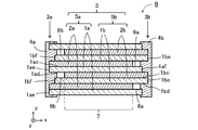
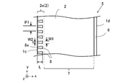
- FIG. 3 is an exploded perspective view schematically showing a wound film capacitor.
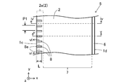
- 1 is a schematic cross-sectional view of a laminated film capacitor. It is a top view of the surface which shows a part of dielectric film and metal film in one of the embodiments. It is the iv-iv sectional view taken on the line of FIG.
- FIG. 5 is a cross-sectional view taken along the line vv of FIG. 3; It is the vi-vi line sectional view of FIG.
- It is a top view of the surface which shows a part of dielectric film and metal film in one of the embodiments.
- It is a top view of the surface which shows a part of dielectric film and metal film in one of the embodiments.
- the film capacitor comprises a film capacitor main body 3 (hereinafter sometimes referred to simply as the main body 3) and a pair of external electrodes 4a and 4b.
- a first dielectric film 1a, a second dielectric film 1b, a first metal film 2a, and a second metal film 2b are stacked or wound.
- the pair of external electrodes 4a and 4b are provided on opposite ends (main body ends) 3a and 3b of the main body 3 by metallikon.
- the main portion 3 of the wound film capacitor A shown in FIG. 1 comprises a first metallized film 5a having the first metal film 2a on the first surface 1ac of the first dielectric film 1a, and a second dielectric film
- the second metallized film 5b provided with the second metal film 2b is stacked and wound on the second surface 1bc of 1b.
- the first metal film 2 a is electrically connected to the external electrode 4 a at one main body end 3 a of the main body 3.
- the second metal film 2 b is electrically connected to the external electrode 4 b at the other main body end 3 b of the main body 3.
- the first of the first dielectric film 1a, the first metal film 2a, and the first metallized film 5a may be omitted, and may simply be referred to as the dielectric film 1a, the metal film 2a, and the metallized film 5a.
- the second of the second dielectric film 1b, the second metal film 2b and the second metallized film 5b may be omitted, and may simply be referred to as the dielectric film 1b, the metal film 2b and the metallized film 5b.
- the drawn dielectric films 1a and 1b and the metal films 2a and 2b are drawn to be thick enough to be in front of the paper.
- the width direction of the dielectric films 1a and 1b and the metal films 2a and 2b is illustrated as a first direction x, the length direction as a second direction y, and the thickness direction as a z direction.
- the first direction x may be simply referred to as the x direction
- the second direction y may be simply referred to as the y direction.
- the dielectric films 1a and 1b and the metal films 2a and 2b are stacked in the z direction.
- the external electrodes 4a and 4b are disposed at the body end portions 3a and 3b located in the x direction of the body portion 3, respectively.
- the x direction coincides with the winding axial direction.
- the main part 3 of the laminated film capacitor B shown in FIG. 2 is a metallized film 5a having the metal film 2a on the first surface 1ac of the dielectric film 1a and a metal film on the second surface 1bc of the dielectric film 1b.
- Metallized films 5b provided with 2b are alternately laminated.
- the metal film 2 a is electrically connected to the external electrode 4 a at one main body end 3 a of the main body 3.
- the metal film 2 b is electrically connected to the external electrode 4 b at the other main body end 3 b of the main body 3.
- the dielectric film 1a of the film capacitors A and B has a first surface 1ac and a third surface 1ad opposed in the z direction, and a first side surface 1ae and a second side surface 1af opposed in the x direction.
- the dielectric film 1b has a second surface 1bc and a fourth surface 1bd opposite in the z direction, and a first side surface 1be and a second side surface 1bf opposite in the x direction.
- the metallized film 5a is obtained by forming the metal film 2a on the first surface 1ac of the dielectric film 1a, and an insulation margin continuously extending in the y direction in the vicinity of the second side surface 1af on the first surface 1ac. It has the part 6a.
- the insulation margin portion 6a is a portion where the dielectric film 1a is exposed.
- the metallized film 5b is obtained by forming the metal film 2b on the second surface 1bc of the dielectric film 1b, and an insulation margin continuously extending in the y direction in the vicinity of the second side surface 1bf on the second surface 1bc. It has the part 6b.
- the insulation margin portion 6 b is a portion where the dielectric film 1 b is exposed.
- the metallized films 5 a and 5 b are laminated or wound in a state of being slightly deviated in the width direction (x direction).
- the reference numerals a and b may be omitted.
- the z-direction which is the thickness direction of the film is enlarged and shown to facilitate the description.
- the film thickness of the metal film 2 may be, for example, 20 nm or less, in particular, 5 to 15 nm. By setting the metal film 2 to such a film thickness, the area resistance becomes 18 to 50 ⁇ / ⁇ , and the self-healing property can be exhibited. Area resistance may be called sheet resistance.
- a metal or alloy such as aluminum (Al) or zinc (Zn) may be used.
- the film thickness of the metal film 2 may be confirmed by, for example, a cross section of the metallized film 5 subjected to the ion milling process with a scanning electron microscope (SEM) or the like.
- SEM scanning electron microscope
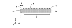
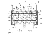
- FIG. 3 is a plan view of the metallized film 5
- FIG. 4 is a cross-sectional view taken along line iv-iv of FIG. 3
- FIG. 5 is a cross-sectional view taken along line v-v of FIG. FIG.
- the metal film 2 has a so-called heavy edge structure at least in the vicinity (2e) of the connection portion with the external electrode 4.
- the vicinity of the connection portion with the external electrode 4 is, in other words, the vicinity of the first side face 1 e of the dielectric film 1.
- the vicinity 2e of the connection portion between the metal film 2 and the external electrode 4 may be referred to as a heavy edge portion 2e or a first portion 2e.
- the heavy edge structure is, for example, a structure in which the thickness of the metal film 2 in the vicinity 2e of the connection portion with the external electrode 4 is large and the electric resistance is low, with respect to the effective region 7 where the metal films 2a and 2b overlap.
- the film thickness of the metal film 2 in the vicinity 2e of the connection portion with the external electrode 4 may be, for example, twice or more, specifically 20 nm or more, of the film thickness capable of exhibiting the self-healing property.
- the film thickness of the metal film 2 in the heavy edge portion 2e may be in the range of 80 nm or less.
- the equivalent series resistance (ESR) of the film capacitors A and B can be reduced by being electrically connected to the external electrode 4 by the heavy edge portion 2e having a low resistance.
- the heavy edge 2e of the metallized film 5a overlaps the insulation margin 6b of the metallized film 5b, and the heavy edge 2e of the metallized film 5b is the insulation margin of the metallized film 5a It may overlap with 6a.
- the width of the heavy edge portion 2e in the first direction x may be, for example, 4 mm or less, particularly 0.5 mm or more and 3 mm or less, depending on the size of the film capacitors A and B.
- the film thickness of the metal film 2 is thick, the influence of the difference between the thermal contraction rate of the metal film 2 and the thermal contraction rate of the dielectric film 1 is large. Therefore, at the end in the x direction of the metallized film 5, that is, at the main body end 3, warpage may occur in the metallized film 5 due to the thermal contraction difference between the metal film 2 and the dielectric film 1.
- the metallized film 5 has a warp at the end 3 of the main body, metallikon hardly enters the gap between the overlapping metallized films 5. As a result, the contact area between the metal film 2 and the external electrode 4 may be reduced, and the electrical connection between the metal film 2 and the external electrode 4 may not be sufficiently obtained.
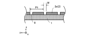
- the metal film 2 has the first groove 8 extending in the first direction x in the heavy edge portion 2e.
- the first groove 8 has an opening 8 e opening at the body end 3 and has a predetermined length L in the first direction x from the opening 8 e.
- the length L of the first direction x of the first groove 8 may be the same as or shorter than the width of the heavy edge portion 2e in the first direction x as shown in FIG.
- the metal film 2 may have a plurality of first grooves 8 at predetermined intervals in the second direction y.
- the heavy edge portion 2 e having the first groove 8 By the heavy edge portion 2 e having the first groove 8, the influence of the thermal contraction difference between the metal film 2 and the dielectric film 1 at the heavy edge portion 2 e is alleviated by the first groove 8, and the metallized film 5 is obtained. Warpage of the end can be made less likely to occur. As a result, the reliability of the electrical connection between the metal film 2 and the external electrode 4 is improved, the dielectric loss of the film capacitor is reduced, and the increase of the dielectric loss due to charge and discharge cycles can be suppressed.
- the length L of the first direction x of the first groove 8 may be equal to or less than the width of the heavy edge portion 2e, that is, the first portion 2e in the first direction x.
- L may be, for example, 1.0 mm or more and 2.0 mm or less.
- L is larger than 1.0 mm, the influence of the thermal contraction difference with the dielectric film 1 can be alleviated.
- L is smaller than 2.0 mm, it is difficult for the first groove 8 to reach the effective area 7, and the capacitance can be secured. That is, the metal film 2 located in the effective region 7 may not have the first groove 8.
- the first groove 8a of the metallized film 5a may overlap with the margin portion 6b of the metallized film 5b and may not overlap with the metal film 2b.
- the first groove 8b of the metallized film 5b may overlap with the margin portion 6a of the metallized film 5a and may not overlap with the metal film 2a. That is, the first groove 8a of the metallized film 5a may not have a portion overlapping with the metal film 2b, and the first groove 8 of the metallized film 5b may not have a portion overlapping with the metal film 2a.
- the distance P1 between the first groove 8 and the first groove 8 adjacent in the second direction y may be, for example, 4 mm or less. If P1 is larger than 4 mm, there is a concern that the influence of the thermal contraction difference between the metal film 2 and the dielectric film 1 can not be alleviated. When the film thickness of the heavy edge portion 2e is relatively large, P1 may be decreased, and when the film thickness of the heavy edge portion 2e is relatively small, P1 may be increased. P1 may be, for example, 1 mm or more, but may be smaller than that.
- the width of the first groove 8 in the second direction y is W, as shown in FIG.
- W1 and W2 may be the same as shown in FIG.
- W1 may be larger than W2, that is, the width W2 of the opening 8e may be narrow, and the width W may be maximum at a portion of the first groove 8 other than the opening 8e.
- the shape of the first groove 8 may be rectangular as shown in FIG. 3, or as shown in FIG. 7, the opening 8e is a short bottom, and the side facing the opening 8e is a long bottom It may be trapezoidal.
- the shape of the first groove 8 may be a cross shape in which a groove extending in the first direction x and a groove extending in the second direction y intersect as shown in FIG.
- the length in the second direction y of the groove extending in the second direction y is taken as the maximum width W1.
- the metal film 2 which is the wall surface of the first groove 8 may be in contact with the main body end 3 across the first groove 8.
- the metal film 2 which is the wall surface of the first groove 8 at the body end 3 may not be joined.
- the shape of the first groove 8 may be a triangular shape having an apex at the body end 3.
- the ratio of the distance P1 between the adjacent first grooves 8 to the width W2 of the opening 8e is W2 / P1.
- W2 / P1 may be, for example, 0.35 or less.
- W1 may be, for example, 0.1 mm or more and 1.0 mm or less, particularly 0.3 mm or more and 0.5 mm or less.
- W2 may be, for example, 1.0 mm or less, in particular 0.5 mm or less.
- the bottom surface of the first groove 8 may be the dielectric film 1.
- the bottom surface of the first groove 8 may be the metal film 2.
- the thickness of the metal film 2 at the bottom of the first groove 8 is smaller than the thickness of the heavy edge 2 e.
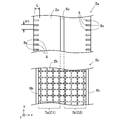
- the metal film 2 may have one or more second grooves 9 in the effective region 7 in addition to the first grooves 8 as shown in FIG.
- the second groove 9 may be in contact with the end face 1 c of the dielectric film 1 and / or the insulation margin 6.
- the second groove 9 may extend in the first direction x and connect the end face 1 c of the dielectric film 1 and the insulation margin portion 6.
- the plurality of second grooves 9 may extend in different directions and intersect each other to divide the metal film 2 into a plurality of small regions.
- the metal film 2 may have a fuse portion 10 connecting the small regions divided by the second groove 9. When there are a plurality of second grooves 9 in the first region 2 e, one or more first grooves 8 may be disposed between the adjacent second grooves 9 and the second grooves 9.
- the distance P 1 between the first groove 8 and the first groove 8 is smaller than the distance P 2 between the second groove 9 and the second groove 9.
- the effective area 7 is divided into two in the first direction x
- the area adjacent to the insulation margin 6 of the metal film 2 has the second groove 9 and the heavy edge 2 e of the metal film 2.
- the region of H may not have the second groove 9.
- the width of the second groove 9 may be, for example, 0.01 to 0.20 mm.
- the second metallized film 5 b having the second metal film 2 b is alternately laminated on the second surface 1 bc of the film 1 b.
- the width direction of the first dielectric film 1a, the second dielectric film 1b, the first metal film 2a, and the second metal film 2b is the first direction x
- the length direction is the second direction y
- the thickness The direction is shown as the z direction.
- the film capacitor C has two capacitive parts connected in series.
- the metal film 2a has a metal film 2a1 located on the left side of FIG. 11 and a metal film 2a2 located on the right side of FIG. That is, the metal film 2a has two metal films 2a1 and 2a2 arranged in the x direction.
- the metal film 2a1 is electrically connected to the external electrode 4a at the main body end 3a located on the left side of the main body portion 3, and the metal film 2a2 is connected to the external electrode 4b at the main body end 3b located on the right side of the main body 3 It is electrically connected.
- the metallized film 5a of the film capacitor C has a first insulation margin portion 6a continuously extending in the second direction y at a central portion in the first direction x.
- the metal film 2 is not formed, and the first surface 1ac is exposed.
- the metal film 2a1 and the metal film 2a2 are electrically insulated by the first insulation margin portion 6a.
- the metallized film 5b of the film capacitor C has a second insulation margin portion 6b continuously extending in the second direction y at both ends in the first direction x.
- the metal film 2 is not formed in the second insulation margin portion 6b, and the second surface 1bc is exposed.
- the metal film 2b is not electrically connected to any of the external electrodes 4a and 4b.
- the dielectric films 1a and 1b and the metal films 2a and 2b are stacked in the z direction and stacked as shown in FIG.
- the first capacity portion C1 and the second capacity portion C2 are connected in series.
- the first capacitance portion C1 is formed in the effective region 7a in which the metal film 2a1 and the metal film 2b sandwich the dielectric film 1a or 1b, and in the second capacitance portion C2, the metal film 2a2 and the metal film 2b are dielectrics It is formed in the effective area 7b sandwiching the body film 1a or 1b.
- any one of the overlapping metal films 2a (2a1, 2a2) and 2b may have a thickness that can exhibit self-healing properties.
- the entire metal film 2a of the film capacitor C may have the same thickness as that of the first portion 2e, and the total thickness of the metal film 2b may be 20 nm or less.
- the film capacitor C can exhibit self-healing property by the metal film 2b.
- the metal film 2a may have only the first groove 8 and the metal film 2b may have the second groove 9.
- Such a series type structure is not only applied to the laminated film capacitor C shown in FIGS. 10 and 11, but may be applied to a wound film capacitor.
- the first capacitance C1 and the second capacitance C2 are connected in series inside the film capacitor, and the voltage applied to the first capacitance C1 and the second capacitance The voltage applied to the part C2 is distributed according to the capacitance of each capacitive part. As a result, the withstand voltage of the entire film capacitor C can be improved.
- the film capacitors A and B may be referred to as a normal film capacitor, and the film capacitor C may be referred to as a series-connected film capacitor.
- the material of the insulating resin used for the dielectric film 1 is, for example, polypropylene (PP), polyethylene terephthalate (PET), polyphenylene sulfide (PPS), polyethylene naphthalate (PEN), polyarylate (PAR), polyphenylene ether (PPE) And polyetherimide (PEI) and cycloolefin polymer (COP).
- PP polypropylene
- PET polyethylene terephthalate
- PPS polyphenylene sulfide
- PEN polyethylene naphthalate
- PAR polyarylate
- PPE polyphenylene ether
- PEI polyetherimide
- COP cycloolefin polymer
- Polyarylates (PAR) in particular have high breakdown voltages.
- Such film capacitors A, B and C may be produced, for example, as follows.
- dielectric film 1 is prepared.
- the dielectric film 1 is formed, for example, by forming a resin solution in which an insulating resin is dissolved in a solvent on a surface of a substrate film made of polyethylene terephthalate (PET), for example, and drying to evaporate the solvent. can get.
- PET polyethylene terephthalate
- the forming method may be appropriately selected from known film forming methods such as a doctor blade method, a die coater method, and a knife coater method.
- a solvent used for molding for example, methanol, isopropanol, n-butanol, ethylene glycol, ethylene glycol monopropyl ether, methyl ethyl ketone, methyl isobutyl ketone, xylene, propylene glycol monomethyl ether, propylene glycol monomethyl ether acetate, dimethyl acetamide, cyclohexane
- an organic solvent containing a mixture of two or more selected from these Alternatively, a film of resin produced by a melt extrusion method may be stretched.
- the thickness of the dielectric film 1 may be, for example, 5 ⁇ m or less. In particular, it is preferable to use a dielectric film 1 having a thickness of 0.5 to 4 ⁇ m.
- the dielectric film 1 may be made of only the above-described insulating resin.
- the dielectric film 1 may contain materials other than the above-mentioned insulating resin.
- components other than resin contained in the dielectric film 1 the above-mentioned organic solvent and an inorganic filler are mentioned, for example.
- the inorganic filler for example, inorganic oxides such as alumina, titanium oxide and silicon dioxide, inorganic nitrides such as silicon nitride, and glass may be used.
- the inorganic filler may be subjected to surface treatment such as silane coupling treatment or titanate coupling treatment.
- the dielectric film 1 When such an inorganic filler is used for the dielectric film 1, a composite film containing less than 50% by mass of the inorganic filler and 50% by mass or more of the resin is used to maintain the flexibility of the resin while maintaining the flexibility. An effect such as improvement of the relative dielectric constant can be obtained.
- the size of the inorganic filler for example, the average particle size may be 4 to 1000 nm.
- a mask is applied to a predetermined portion of one surface of the produced dielectric film 1.
- a metal component such as aluminum (Al) is vapor-deposited on the non-masked portion of one surface of the dielectric film 1 to form the metal film 2, thereby obtaining the metallized film 5 having the insulation margin portion 6.
- the predetermined portion to be masked is one of the ends in the width direction (first direction x).
- the predetermined portion is the central portion in the width direction (first direction x) of the first dielectric film 1a, and both in the width direction (first direction x) of the second dielectric film 1b.
- the heavy edge structure is formed by masking, for example, zinc (Zn) further on the non-masked portion of the vapor-deposited metal component described above except for the portion forming the heavy edge of the metallized film 5 described above.
- the film thickness of the vapor deposition film to be vapor deposited to form the heavy edge portion 2e may be 1 to 3 times the film thickness of the above-mentioned vapor deposited metal component. As a result, the film thickness of the heavy edge portion 2e is 2 to 4 times the film thickness of the other portion, and becomes the first portion 2e.
- the first groove 8 is formed in the first portion 2 e of the metal film 2.
- Laser patterning may be used to form the first groove 8.
- the laser patterning method is a method of evaporating a part of the metal film 4 by a laser, and uses a laser marker machine or a laser trimmer machine.
- the laser any one of a green laser, a YAG laser and a CO 2 laser may be used.
- the metallized film 5 (5a, 5b) having the metal film 2 (2a, 2b) on one side is a little in the width direction, ie, in the first direction x, as shown in FIG.
- the main body 3 of the film capacitor A or B is obtained by stacking one or more sets in a shifted state and laminating or winding.
- the main body 3 of the film capacitor C is obtained by stacking the metallized films 5a and 5b as a set, and stacking one or more sets as shown in FIG. 11, or winding.
- Film capacitors A, B, or C can be obtained by forming metallikon electrodes as external electrodes 4 on both end surfaces of the obtained main body portion 3 in the x direction.
- a method such as thermal spraying of metal, sputtering, plating or the like may be used.
- the outer surface of the main body 3 on which the external electrode 4 is formed may be covered with an exterior member (not shown).
- Examples of the material of the metal film 2 include metals or alloys such as aluminum (Al) and zinc (Zn).
- At least one metal material selected from zinc, tin, aluminum, copper and solder may be used as the material of the metallikon electrode.
- FIG. 12 is a perspective view schematically showing one of the embodiments of the coupled capacitor.
- the connection type capacitor D a plurality of wound film capacitors A are connected in parallel by a pair of bus bars 21 and 23.
- the bus bars 21 and 23 have terminal portions 21 a and 23 a for external connection and lead terminal portions 21 b and 23 b.
- the leadout terminal portions 21b and 23b are respectively connected to the external electrodes 4a and 4b of the film capacitor A.
- connection type capacitor D may include a laminated type film capacitor B or a series connection type film capacitor C in place of the wound type film capacitor A.
- the connected capacitor D may have at least one film capacitor A, or may have two or more film capacitors A.
- the connection type capacitor D in a state where a plurality of film capacitors A are arranged, for example, four as shown in FIG. 12, the external electrodes 4a and 4b respectively formed on both ends of the main body 3 It is obtained by attaching 21 and 23.
- the connected capacitor D may have a flat film capacitor, or may have a stacked film capacitor.
- the film capacitor A may be arranged such that the direction in which the external electrode 4 is located, that is, the x direction is along the vertical direction.
- the film capacitors A, B and C and the connected capacitor D may be housed in a case and then filled with resin in the space in the case to form a resin mold type (case mold type) capacitor.
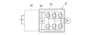
- FIG. 13 is a schematic configuration diagram for describing an embodiment of an inverter.
- FIG. 13 shows an inverter E that generates alternating current from direct current as an example of the embodiment.
- the inverter E includes a bridge circuit 31 and a capacitance unit 33, as shown in FIG.
- the bridge circuit 31 includes, for example, a switching element such as an IGBT (Insulated gate Bipolar Transistor) and a diode.
- the capacitive unit 33 is disposed between the input terminals of the bridge circuit 31 to stabilize the voltage.
- the above-described film capacitors A, B, and C or a connection type capacitor D are used as the capacitor portion 33.
- the inverter E is connected to a booster circuit 35 that boosts the voltage of the DC power supply.
- the bridge circuit 31 is connected to a motor generator (motor M) as a driving source.
- FIG. 14 is a schematic block diagram of an electric vehicle.
- FIG. 14 shows a hybrid vehicle (HEV) as an example of the embodiment.
- HEV hybrid vehicle
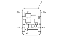
- the electric powered vehicle F includes a drive motor 41, an engine 43, a transmission 45, an inverter 47, a power supply (battery) 49, a front wheel 51a and a rear wheel 51b.
- the electric powered vehicle F is provided with an output of a motor 41, an engine 43, or both as a drive source.
- the output of the drive source is transmitted to the pair of left and right front wheels 51 a via the transmission 45.
- the power supply 49 is connected to the inverter 47, and the inverter 47 is connected to the motor 41.
- the electric powered vehicle F shown in FIG. 14 includes a vehicle ECU 53 and an engine ECU 57.
- the vehicle ECU 53 performs overall control of the entire electric powered vehicle E.
- the engine ECU 57 controls the rotational speed of the engine 43 to drive the electric vehicle E.
- the electric powered vehicle E further includes an ignition key 55 operated by a driver or the like, an accelerator pedal (not shown), and a driving device such as a brake.
- the vehicle ECU 53 receives a drive signal according to the operation of the drive device by the driver or the like.
- the vehicle ECU 53 outputs an instruction signal to the engine ECU 57, the power supply 49, and the inverter 47 as a load based on the drive signal.
- Engine ECU 57 controls the number of rotations of engine 43 in response to the instruction signal, and drives electrically powered vehicle E.
- an inverter E that is, the inverter E including the above film capacitors A, B, C or a coupled capacitor D in the capacity portion 33 is used.
- the film capacitors A, B, C or the coupled capacitor D have small dielectric loss and little increase in dielectric loss due to charge and discharge cycles, so the electrostatic capacitance is extended for a long time The switching noise generated by the inverter 47 can be reduced for a long time.
- the inverter E of this embodiment can be applied not only to the above-mentioned hybrid vehicle (HEV) but also to various power conversion application products such as an electric vehicle (EV), a fuel cell vehicle, or an electric bicycle, a generator, a solar cell .
- EV electric vehicle
- a fuel cell vehicle or an electric bicycle
- a generator a solar cell .
- a dielectric film having an average thickness of 2.5 ⁇ m was produced using polyarylate (U-100, manufactured by Unitika).
- the dielectric film was prepared by dissolving polyarylate in toluene, applying it on a substrate made of polyethylene terephthalate (PET) using a coater, and forming it into a sheet. After molding, heat treatment was performed at 130 ° C. to remove toluene, and a dielectric film was obtained. The obtained dielectric film was peeled from the substrate and slit into a width of 130 mm.
- a series connected film capacitor was produced as follows.
- An Al (aluminum) metal film was formed on one main surface of the dielectric film to obtain a metallized film having two types of metal films different in film thickness.
- a thick metal film is referred to as a first metal film
- a thin metal film is referred to as a second metal film.
- the film thickness of the metal film was determined by scanning electron microscope (SEM) observation of a cross section subjected to ion milling.
- the film thickness t1 of the first metal film and the film thickness t2 of the second metal film are shown in Table 1.
- the sheet resistance was evaluated in a 4-terminal resistance measurement mode using a multimeter. For example, the sheet resistance of the metal film with a film thickness of 50 nm was 7 ⁇ / ⁇ , and the sheet resistance of the metal film with a film thickness of 30 nm was 25 ⁇ / ⁇ .
- a 2 mm wide first insulation margin is formed at the center of the first metal film in the first direction x using a green laser marker, and the second insulation margin is formed at both ends of the second metal film in the first direction x Formed.
- the first groove was formed at both ends in the first direction x of the thick first metal film, that is, at the first portion.
- the shape of the first groove is shown in Table 1.
- a second groove was formed in a mesh shape on the entire surface using a green laser marker.
- a second groove formed a pattern composed of a small area of 2 mm ⁇ 2 mm and a fuse part having a width of 0.2 mm connecting the small areas.
- the laser irradiation conditions were an output of 4 W, a frequency of 140 kHz, and a scanning speed of 4 m / sec.
- a 130 mm wide metallized film is further slitted, and a first metallized film having a first metal film is a 28 mm wide metallized film having a first insulation margin portion with a width of 2 mm at a central portion in a first direction x.
- the second metallized film having the second metal film was a metallized film with a total width of 27 mm, having a second insulation margin portion with a width of 1.5 mm at both ends in the first direction x.
- the first metallized film and the second metallized film were superposed, and wound 100 times on a drum with a diameter of 200 mm, to obtain a wound body in which a plurality of film capacitors are annularly connected.
- the first metallized film and the second metallized film were laminated so as to sandwich a single dielectric film between the first metal film and the second metal film.
- the conventional film capacitor was produced as follows. An oil mask was used on one surface of the dielectric film slitted to a width of 130 mm, and an Al (aluminum) metal film having a width of 52 mm was formed at the center in the width direction which is the first direction x. The average thickness of the Al metal film was 15 nm. Next, a Zn (zinc) metal film having a width of 2 to 8 mm was formed at the center in the width direction of the formed Al metal film as a heavy edge portion using a metal mask. The average thickness of the Zn metal film was 5 to 65 nm.
- the center and both ends in the width direction of the obtained metallized film were slit to obtain a first metallized film and a second metallized film having a width of 28 mm.
- the width of the insulation margin of each metallized film obtained was 1 mm, and the width of the heavy edge was 1 to 4 mm.
- a first groove was formed in the heavy edge portion or first portion of the first metal film and the second metal film using a green laser marker.
- the shape of the first groove is shown in Table 2.
- a second groove is formed in a mesh shape using a green laser marker in a region closer to the insulation margin portion than the center of the first metal film and the second metal film in the first direction, and a small 2 mm ⁇ 2 mm
- a pattern was formed of a region and a 0.2 mm wide fuse portion connecting between the small regions.
- the laser irradiation conditions were an output of 4 W, a frequency of 140 kHz, and a scanning speed of 4 m / sec.
- the heavy edge portions of the first metallized film and the second metallized film are located on the opposite side of the first direction x, and the respective heavy edge portions protrude 0.5 mm in the first direction x , Overlaid.
- One set of the metallized films thus stacked was wound 100 times on a drum having a diameter of 200 mm to obtain a wound body in which a plurality of film capacitors were connected in an annular shape.
- the first metallized film and the second metallized film were laminated so as to sandwich a single dielectric film between the first metal film and the second metal film.
- the obtained wound body was cut so that the width in the second direction y was 15 mm, to obtain a laminate as a main body.
- An alloy of zinc and tin was sprayed on the end face of the main body in the first direction x to form a metallikon electrode as an external electrode to obtain a film capacitor.
- the dielectric loss (DF) of the produced film capacitor was measured using a digital multimeter under conditions of 1 V AC and 1 kHz. The value of this dielectric loss is taken as dielectric loss DF1 before the charge and discharge test.
- the charge / discharge test of the film capacitor was performed as follows. After charging the film capacitor with a DC voltage (DC) of 600 V, a forced short circuit was performed to discharge. A charge / discharge test of 100 cycles was performed on a charge / discharge cycle in which one charge-discharge cycle was one cycle. After the charge and discharge test, the dielectric loss DF was measured again, and the obtained value was taken as the dielectric loss DF2 after the charge and discharge test.
- the values of DF1, DF2 and DF2 / DF1 are listed in Table 1.
- DF2 / DF1 is the ratio of DF2 to DF1.
- Sample No. 1 having a first groove at the end in the first direction of the thick first metal film that is, the first portion. 2, 3, 5 to 17, 19, 20, and a sample No. 1 having a heavy edge portion, ie, a first groove at a first portion. 22, 23, 25, 26, 28 to 36, 38, 40 and 41 have sample Nos. 1 and 2 that do not have a first groove.
- the increase in dielectric loss after the charge and discharge test was small.
- sample No. 1 in which the maximum width W1 of the first groove is larger than the width W2 of the opening portion No increase in dielectric loss was observed after the charge / discharge test in any of 3, 14, 16 to 20, 23, 26, 33 to 35 and 41.
- A, B, C film capacitor D: connected capacitor E: inverter F: electric vehicle 1, 1a, 1b: dielectric film 2, 2a, 2b: metal film 2e: first portion (heavy edge portion) 3: Body part 4, 4a, 4b: External electrode 5, 5a, 5b: Metallized film 7: Effective area 8: First groove 9: Second groove 10: Fuse part 21, 23: Bus bar 31: Bridge circuit 33: Capacity section 35: Boost circuit 41: Motor 43: Engine 45: Transmission 47: Inverter 49: Power supply 51a: Front wheel 51b: Rear wheel 53: Vehicle ECU 55: Ignition key 57: Engine ECU
Landscapes
- Engineering & Computer Science (AREA)
- Power Engineering (AREA)
- Microelectronics & Electronic Packaging (AREA)
- Manufacturing & Machinery (AREA)
- Fixed Capacitors And Capacitor Manufacturing Machines (AREA)
- Inverter Devices (AREA)
Abstract
Description


D :連結型コンデンサ
E :インバータ
F :電動車輌
1、1a、1b:誘電体フィルム
2、2a、2b:金属膜
2e :第1部位(ヘビーエッジ部)
3 :本体部
4、4a、4b:外部電極
5、5a、5b:金属化フィルム
7 :有効領域
8 :第1の溝
9 :第2の溝
10 :ヒューズ部
21、23 :バスバー
31 :ブリッジ回路
33 :容量部
35 :昇圧回路
41 :モータ
43 :エンジン
45 :トランスミッション
47 :インバータ
49 :電源
51a :前輪
51b :後輪
53 :車輌ECU
55 :イグニッションキー
57 :エンジンECU
Claims (13)
- 第1誘電体フィルム、および該第1誘電体フィルムの第1面上に配置された第1金属膜を有する第1金属化フィルムと、第2誘電体フィルム、および第2誘電体フィルムの第2面上に配置された第2金属膜を有する第2金属化フィルムと、を少なくとも備える本体部と、一対の外部電極と、を具備し、
前記第1金属膜と前記第2金属膜との間には、前記第1誘電体フィルムまたは前記第2誘電体フィルムが配置され、
前記外部電極は、前記本体部の第1方向の一対の本体端部にそれぞれ配置され、前記第1金属膜および前記第2金属膜のいずれか一方に電気的に接続され、
前記第1金属膜および/または前記第2金属膜は、前記外部電極と電気的に接続する前記本体端部の近傍に、膜厚が20nm以上の第1部位を有するとともに、該第1部位に、前記本体端部に接し、前記第1方向に延びる第1の溝を有する、フィルムコンデンサ。 - 前記第1金属膜が前記第1の溝を有し、
前記第1金属化フィルムおよび前記第2金属化フィルムを厚さ方向に平面視した時、
前記第1金属膜の前記第1の溝と、前記第2金属膜とが重なる部位を有さない、請求項1に記載のフィルムコンデンサ。 - 前記第1の溝の前記第1方向の長さが、前記第1部位の前記第1方向の幅以下である、請求項1または2に記載のフィルムコンデンサ。
- 前記第1方向に直交する第2方向における前記第1の溝の幅をWとし、Wの最大値をW1とし、前記第1の溝の前記本体端部に接する部位の幅をW2としたとき、
W1がW2よりも大きい、請求項1~3のいずれかに記載のフィルムコンデンサ。 - 前記第1の溝は、前記第1金属化フィルムおよび/または前記第2金属化フィルムの厚さ方向に位置する底面を有するとともに、該底面に、前記第1金属膜または前記第2金属膜を有する、請求項1~4のいずれかに記載のフィルムコンデンサ。
- 前記第1の溝は、前記第1金属化フィルムおよび/または前記第2金属化フィルムの厚さ方向に位置する底面を有するとともに、該底面に、前記第1誘電体フィルムまたは前記第2誘電体フィルムを有する、請求項1~5のいずれかに記載のフィルムコンデンサ。
- 前記第2金属膜が前記第1の溝を有し、
前記第1金属化フィルムおよび前記第2金属化フィルムを厚さ方向に平面視した時、
前記第2金属膜の前記第1の溝と、前記第1金属膜とが重なる部位を有さない、請求項1~6のいずれかに記載のフィルムコンデンサ。 - 前記第1金属化フィルムは、前記第1面上の前記第1方向の中央部に第1絶縁マージン部を有し、
前記第2金属化フィルムは、前記第2面上の前記第1方向の両端部に第2絶縁マージン部を有し、
前記第1絶縁マージン部および第2絶縁マージン部は、前記第1金属膜および前記第2金属膜を有さない部分であり、前記第1方向に直交する第2方向に連続して延びており、
前記第1金属膜が、前記第1絶縁マージン部の前記第1方向の両側に存在するとともに、前記本体端部でそれぞれ前記外部電極に電気的に接続され、
前記第2金属膜が、前記外部電極のいずれにも電気的に接続されない、請求項1~6のいずれかに記載のフィルムコンデンサ。 - 前記第1金属膜の厚さをt1とし、前記第2金属膜の厚さをt2とした時、前記t1が前記t2より大きい、請求項8に記載のフィルムコンデンサ。
- 前記t2に対する前記t1の比率(t1/t2)が、2以上4以下である、請求項9に記載のフィルムコンデンサ。
- 複数のフィルムコンデンサと、該複数のフィルムコンデンサを電気的に接続するバスバーと、を備え、前記フィルムコンデンサが、請求項1~10のいずれかに記載のフィルムコンデンサを含む、連結型コンデンサ。
- スイッチング素子を有するブリッジ回路と、該ブリッジ回路に接続された容量部とを備え、前記容量部が請求項1~10のいずれかに記載のフィルムコンデンサを含む、インバータ。
- 電源と、該電源に接続されたインバータと、該インバータに接続されたモータと、該モータにより駆動する車輪と、を備え、前記インバータが、請求項12に記載のインバータである、電動車輌。
Priority Applications (4)
| Application Number | Priority Date | Filing Date | Title |
|---|---|---|---|
| JP2019551202A JP6938662B2 (ja) | 2017-10-27 | 2018-10-24 | フィルムコンデンサ、連結型コンデンサと、これを用いたインバータおよび電動車輌 |
| US16/755,682 US11631545B2 (en) | 2017-10-27 | 2018-10-24 | Film capacitor, combination type capacitor, and inverter and electric vehicle employing the same |
| EP18871340.8A EP3703087A4 (en) | 2017-10-27 | 2018-10-24 | FILM CAPACITOR, CONNECTING CAPACITOR AND INVERTER, AND ELECTRIC VEHICLE WITH THESE CAPACITORS |
| CN201880066703.0A CN111213217B (zh) | 2017-10-27 | 2018-10-24 | 薄膜电容器、连结型电容器、使用其的逆变器以及电动车辆 |
Applications Claiming Priority (2)
| Application Number | Priority Date | Filing Date | Title |
|---|---|---|---|
| JP2017208290 | 2017-10-27 | ||
| JP2017-208290 | 2017-10-27 |
Publications (1)
| Publication Number | Publication Date |
|---|---|
| WO2019082929A1 true WO2019082929A1 (ja) | 2019-05-02 |
Family
ID=66247788
Family Applications (1)
| Application Number | Title | Priority Date | Filing Date |
|---|---|---|---|
| PCT/JP2018/039498 Ceased WO2019082929A1 (ja) | 2017-10-27 | 2018-10-24 | フィルムコンデンサ、連結型コンデンサと、これを用いたインバータおよび電動車輌 |
Country Status (5)
| Country | Link |
|---|---|
| US (1) | US11631545B2 (ja) |
| EP (1) | EP3703087A4 (ja) |
| JP (1) | JP6938662B2 (ja) |
| CN (1) | CN111213217B (ja) |
| WO (1) | WO2019082929A1 (ja) |
Cited By (5)
| Publication number | Priority date | Publication date | Assignee | Title |
|---|---|---|---|---|
| CN114586122A (zh) * | 2019-10-30 | 2022-06-03 | 京瓷株式会社 | 薄膜电容器元件 |
| CN114743795A (zh) * | 2022-04-18 | 2022-07-12 | 无锡宸瑞新能源科技有限公司 | 一种交流滤波薄膜电容器及其生产工艺 |
| WO2022202194A1 (ja) * | 2021-03-25 | 2022-09-29 | 京セラ株式会社 | フィルムコンデンサ、連結型コンデンサ、インバータおよび電動車輌 |
| WO2022202193A1 (ja) * | 2021-03-25 | 2022-09-29 | 京セラ株式会社 | フィルムコンデンサ、連結型コンデンサ、インバータおよび電動車輌 |
| JP2023141295A (ja) * | 2022-03-23 | 2023-10-05 | 京セラ株式会社 | フィルムコンデンサ、連結型コンデンサ、インバータおよび電動車輌 |
Families Citing this family (2)
| Publication number | Priority date | Publication date | Assignee | Title |
|---|---|---|---|---|
| WO2022080148A1 (ja) * | 2020-10-16 | 2022-04-21 | 株式会社指月電機製作所 | フィルムコンデンサ |
| US12400797B2 (en) * | 2023-04-27 | 2025-08-26 | GM Global Technology Operations LLC | Low parasitic equivalent series L-inductance (ESL) symmetric direct current (DC) link capacitor |
Citations (5)
| Publication number | Priority date | Publication date | Assignee | Title |
|---|---|---|---|---|
| JPS622513A (ja) * | 1985-06-27 | 1987-01-08 | 松下電器産業株式会社 | Cr複合部品 |
| JP2005085870A (ja) | 2003-09-05 | 2005-03-31 | Matsushita Electric Ind Co Ltd | 金属化フィルムコンデンサ |
| JP2008270331A (ja) * | 2007-04-17 | 2008-11-06 | Matsushita Electric Ind Co Ltd | フィルムコンデンサ |
| JP2013219094A (ja) * | 2012-04-05 | 2013-10-24 | Panasonic Corp | 金属化フィルムコンデンサ |
| JP2015177172A (ja) * | 2014-03-18 | 2015-10-05 | 京セラ株式会社 | フィルムコンデンサ |
Family Cites Families (11)
| Publication number | Priority date | Publication date | Assignee | Title |
|---|---|---|---|---|
| DE3271708D1 (en) * | 1981-01-07 | 1986-07-24 | Matsushita Electric Industrial Co Ltd | Roll type capacitor having segmented metallized areas |
| JPS61287119A (ja) * | 1985-06-13 | 1986-12-17 | 松下電器産業株式会社 | 金属化フイルムコンデンサ |
| FR2598025B1 (fr) * | 1986-04-25 | 1990-10-05 | Precision Lyonnaise | Feuille dielectrique metallisee pour la realisation de condensateurs electriques du type bobine, ainsi que condensateurs obtenus |
| US4694377A (en) * | 1986-05-28 | 1987-09-15 | Aerovox Incorporated | Segmented capacitor |
| JPH02198122A (ja) * | 1989-01-27 | 1990-08-06 | Matsushita Electric Ind Co Ltd | 金属化フィルムコンデンサの製造方法 |
| JP3328477B2 (ja) * | 1995-10-06 | 2002-09-24 | 松下電器産業株式会社 | コンデンサ |
| TW347540B (en) * | 1996-11-22 | 1998-12-11 | Mitsubishi Shindo Kk | Film condenser and metalized film |
| JP3914854B2 (ja) * | 2002-10-10 | 2007-05-16 | 松下電器産業株式会社 | 金属化フィルムコンデンサとそれを用いたインバータ平滑用コンデンサと自動車用コンデンサ |
| US9437364B2 (en) * | 2011-11-11 | 2016-09-06 | Panasonic Intellectual Property Management Co., Ltd. | Film capacitor |
| US10535464B2 (en) * | 2016-03-14 | 2020-01-14 | Kyocera Corporation | Film capacitor, combination type capacitor, and inverter and electric vehicle using the same |
| CN106683885B (zh) * | 2016-12-21 | 2018-09-28 | 南通新江海动力电子有限公司 | 薄膜电容器用金属化薄膜 |
-
2018
- 2018-10-24 WO PCT/JP2018/039498 patent/WO2019082929A1/ja not_active Ceased
- 2018-10-24 JP JP2019551202A patent/JP6938662B2/ja active Active
- 2018-10-24 EP EP18871340.8A patent/EP3703087A4/en not_active Withdrawn
- 2018-10-24 CN CN201880066703.0A patent/CN111213217B/zh active Active
- 2018-10-24 US US16/755,682 patent/US11631545B2/en active Active
Patent Citations (5)
| Publication number | Priority date | Publication date | Assignee | Title |
|---|---|---|---|---|
| JPS622513A (ja) * | 1985-06-27 | 1987-01-08 | 松下電器産業株式会社 | Cr複合部品 |
| JP2005085870A (ja) | 2003-09-05 | 2005-03-31 | Matsushita Electric Ind Co Ltd | 金属化フィルムコンデンサ |
| JP2008270331A (ja) * | 2007-04-17 | 2008-11-06 | Matsushita Electric Ind Co Ltd | フィルムコンデンサ |
| JP2013219094A (ja) * | 2012-04-05 | 2013-10-24 | Panasonic Corp | 金属化フィルムコンデンサ |
| JP2015177172A (ja) * | 2014-03-18 | 2015-10-05 | 京セラ株式会社 | フィルムコンデンサ |
Non-Patent Citations (1)
| Title |
|---|
| See also references of EP3703087A4 |
Cited By (10)
| Publication number | Priority date | Publication date | Assignee | Title |
|---|---|---|---|---|
| CN114586122A (zh) * | 2019-10-30 | 2022-06-03 | 京瓷株式会社 | 薄膜电容器元件 |
| WO2022202194A1 (ja) * | 2021-03-25 | 2022-09-29 | 京セラ株式会社 | フィルムコンデンサ、連結型コンデンサ、インバータおよび電動車輌 |
| JPWO2022202194A1 (ja) * | 2021-03-25 | 2022-09-29 | ||
| WO2022202193A1 (ja) * | 2021-03-25 | 2022-09-29 | 京セラ株式会社 | フィルムコンデンサ、連結型コンデンサ、インバータおよび電動車輌 |
| JPWO2022202193A1 (ja) * | 2021-03-25 | 2022-09-29 | ||
| JP7663675B2 (ja) | 2021-03-25 | 2025-04-16 | 京セラ株式会社 | フィルムコンデンサ、連結型コンデンサ、インバータおよび電動車輌 |
| JP7663676B2 (ja) | 2021-03-25 | 2025-04-16 | 京セラ株式会社 | フィルムコンデンサ、連結型コンデンサ、インバータおよび電動車輌 |
| JP2023141295A (ja) * | 2022-03-23 | 2023-10-05 | 京セラ株式会社 | フィルムコンデンサ、連結型コンデンサ、インバータおよび電動車輌 |
| CN114743795A (zh) * | 2022-04-18 | 2022-07-12 | 无锡宸瑞新能源科技有限公司 | 一种交流滤波薄膜电容器及其生产工艺 |
| CN114743795B (zh) * | 2022-04-18 | 2023-12-05 | 无锡宸瑞新能源科技有限公司 | 一种交流滤波薄膜电容器及其生产工艺 |
Also Published As
| Publication number | Publication date |
|---|---|
| JPWO2019082929A1 (ja) | 2020-11-19 |
| CN111213217B (zh) | 2021-11-02 |
| JP6938662B2 (ja) | 2021-09-22 |
| EP3703087A4 (en) | 2021-11-10 |
| US20210193393A1 (en) | 2021-06-24 |
| CN111213217A (zh) | 2020-05-29 |
| US11631545B2 (en) | 2023-04-18 |
| EP3703087A1 (en) | 2020-09-02 |
Similar Documents
| Publication | Publication Date | Title |
|---|---|---|
| JP6938662B2 (ja) | フィルムコンデンサ、連結型コンデンサと、これを用いたインバータおよび電動車輌 | |
| JP6688876B2 (ja) | フィルムコンデンサ、連結型コンデンサと、これを用いたインバータおよび電動車輌 | |
| JP6574922B1 (ja) | フィルムコンデンサ、連結型コンデンサ、インバータおよび電動車輌 | |
| JP7011053B2 (ja) | フィルムコンデンサ、連結型コンデンサと、これを用いたインバータ及び電動車輌 | |
| JP6744486B2 (ja) | フィルムコンデンサ、連結型コンデンサと、これを用いたインバータおよび電動車輌 | |
| JP6799588B2 (ja) | フィルムコンデンサ、連結型コンデンサと、これを用いたインバータおよび電動車輌 | |
| JP6687373B2 (ja) | フィルムコンデンサ、連結型コンデンサと、これを用いたインバータおよび電動車輌 | |
| JP6737818B2 (ja) | フィルムコンデンサ、連結型コンデンサ、インバータ、および電動車輌 | |
| CN114041263B (zh) | 层叠型电容器、连结型电容器、逆变器以及电动车辆 |
Legal Events
| Date | Code | Title | Description |
|---|---|---|---|
| 121 | Ep: the epo has been informed by wipo that ep was designated in this application |
Ref document number: 18871340 Country of ref document: EP Kind code of ref document: A1 |
|
| ENP | Entry into the national phase |
Ref document number: 2019551202 Country of ref document: JP Kind code of ref document: A |
|
| NENP | Non-entry into the national phase |
Ref country code: DE |
|
| ENP | Entry into the national phase |
Ref document number: 2018871340 Country of ref document: EP Effective date: 20200527 |
|
| WWW | Wipo information: withdrawn in national office |
Ref document number: 2018871340 Country of ref document: EP |