WO2019087918A1 - Module de cellules solaires - Google Patents
Module de cellules solaires Download PDFInfo
- Publication number
- WO2019087918A1 WO2019087918A1 PCT/JP2018/039651 JP2018039651W WO2019087918A1 WO 2019087918 A1 WO2019087918 A1 WO 2019087918A1 JP 2018039651 W JP2018039651 W JP 2018039651W WO 2019087918 A1 WO2019087918 A1 WO 2019087918A1
- Authority
- WO
- WIPO (PCT)
- Prior art keywords
- solar cell
- protective member
- sealing material
- cell unit
- semiconductor
- Prior art date
- Legal status (The legal status is an assumption and is not a legal conclusion. Google has not performed a legal analysis and makes no representation as to the accuracy of the status listed.)
- Ceased
Links
Images




Classifications
-
- H—ELECTRICITY
- H10—SEMICONDUCTOR DEVICES; ELECTRIC SOLID-STATE DEVICES NOT OTHERWISE PROVIDED FOR
- H10F—INORGANIC SEMICONDUCTOR DEVICES SENSITIVE TO INFRARED RADIATION, LIGHT, ELECTROMAGNETIC RADIATION OF SHORTER WAVELENGTH OR CORPUSCULAR RADIATION
- H10F19/00—Integrated devices, or assemblies of multiple devices, comprising at least one photovoltaic cell covered by group H10F10/00, e.g. photovoltaic modules
- H10F19/80—Encapsulations or containers for integrated devices, or assemblies of multiple devices, having photovoltaic cells
-
- Y—GENERAL TAGGING OF NEW TECHNOLOGICAL DEVELOPMENTS; GENERAL TAGGING OF CROSS-SECTIONAL TECHNOLOGIES SPANNING OVER SEVERAL SECTIONS OF THE IPC; TECHNICAL SUBJECTS COVERED BY FORMER USPC CROSS-REFERENCE ART COLLECTIONS [XRACs] AND DIGESTS
- Y02—TECHNOLOGIES OR APPLICATIONS FOR MITIGATION OR ADAPTATION AGAINST CLIMATE CHANGE
- Y02E—REDUCTION OF GREENHOUSE GAS [GHG] EMISSIONS, RELATED TO ENERGY GENERATION, TRANSMISSION OR DISTRIBUTION
- Y02E10/00—Energy generation through renewable energy sources
- Y02E10/50—Photovoltaic [PV] energy
Definitions
- the present disclosure relates to a solar cell module.
- a solar cell of a stacked type in which a top cell on the front side and a bottom cell on the back side are stacked via a transparent insulating layer from the front side to the back side where light is incident
- a module see, for example, the descriptions of Japanese Patent Application Laid-Open Nos. 2005-277113 and 2010-67752.
- a solar cell module is disclosed.
- One aspect of the solar cell module includes a first protective member, a second protective member, a first solar cell portion, a second solar cell portion, a third protective member, a first sealing material, and a second sealing member. And a stopper.
- the first protective member has translucency.
- the first solar cell unit is located between the first protective member and the second protective member.
- the second solar cell unit is located between the first solar cell unit and the second protective member.
- the third protective member is located between the first solar cell unit and the second solar cell unit, and has a light transmitting property.
- the first sealing material is positioned in a state of covering the first solar cell portion in a first region between the first protective member and the third protective member, and has translucency.
- the second sealing material is positioned in a state of covering the second solar cell portion in a second region between the second protective member and the third protective member, and has a light transmitting property.
- the moisture permeability of the first protective member and the third protective member is lower than the moisture permeability of the first sealing material and the second sealing material.
- One aspect of the solar cell module includes a first protective member, a second protective member, a first solar cell portion, a second solar cell portion, a plate-like third protective member, and a first sealing member. And a second sealing material.
- the first protective member has translucency.
- the first solar cell unit is located between the first protective member and the second protective member.
- the second solar cell unit is located between the first solar cell unit and the second protective member.
- the third protective member is located between the first solar cell unit and the second solar cell unit, and has a light transmitting property.
- the first sealing material is positioned in a state of covering the first solar cell portion in a first region between the first protective member and the third protective member, and has translucency.
- the second sealing material is positioned in a state of covering the second solar cell portion in a second region between the second protective member and the third protective member, and has a light transmitting property.
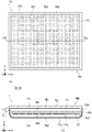
- FIG.1 (a) is a top view which shows the external appearance seen from the front side of an example of the solar cell module which concerns on 1st Embodiment.
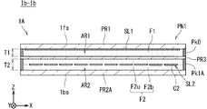
- FIG. 1 (b) is a view showing an example of a virtual cross section of the solar cell module taken along line Ib-Ib of FIG. 1 (a).
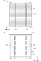
- FIG. 2 is a plan view showing an appearance of an example of the first protective member as viewed from the front side.
- Fig.3 (a) is a top view which shows the structure of an example of a 1st solar cell part.
- FIG. 3 (b) is a view showing an example of a virtual cut surface portion of the first solar cell unit taken along line IIIb-IIIb of FIG. 3 (a).
- FIG. 4 is a plan view showing the structure of an example of the third protective member.
- FIG. 5 is a plan view showing an example of the structure of the second solar cell unit.
- Fig.6 (a) is a top view which shows the structure seen from the 1st element surface side of an example of a 2nd solar cell element.
- FIG.6 (b) is a top view which shows the structure seen from the 2nd element surface side of an example of a 2nd solar cell element.
- FIG. 7 is a plan view showing the structure of an example of the second protective member.
- FIGS. 8 (a) and 8 (b) are virtual cutting plane parts corresponding to the virtual cutting plane part of FIG. 1 (b) in the process of manufacturing the solar cell module according to the first embodiment, respectively.
- FIG. FIG. 9 is a view showing a virtual cut surface portion corresponding to a virtual cut surface portion along the line Ib-Ib of FIG. 1A in an example of the solar cell module according to the second embodiment.
- a tandem-type solar cell module includes, for example, a transparent plate such as a glass plate that constitutes a light receiving surface (also referred to as a front surface), a top cell on the front side to which light transmitted through the transparent plate is incident, and a bottom cell on the back side.
- a transparent plate such as a glass plate that constitutes a light receiving surface (also referred to as a front surface)
- a top cell on the front side to which light transmitted through the transparent plate is incident and a bottom cell on the back side.
- the longitudinal direction (also referred to as a first direction) of the front surface 1 fs described later of the solar cell module 1 is taken as + X direction
- the lateral direction (also referred to as a second direction) of the front surface 1 fs is taken as + Y direction
- the normal direction of the front face 1 fs is the + Z direction.
- the solar cell module 1 mainly includes a light receiving surface (also referred to as a front surface) 1 fs on which light is incident, and a back surface 1 bs opposite to the front surface 1 fs. And.
- the front surface 1 fs is in the state of facing the + Z direction.
- the back surface 1bs is in the state of facing the -Z direction.
- the + Z direction is set to a direction toward the sun, which is in the south.
- the front surface 1 fs and the back surface 1 bs have a rectangular shape.
- the solar cell module 1 includes, for example, a solar cell panel PN1.
- the solar cell module 1 may be provided with a terminal box, a frame, etc., for example.
- the terminal box is located, for example, on the back surface 1bs of the solar cell panel PN1.
- the terminal box can output, for example, the electricity obtained by the power generation in the solar cell panel PN1 to the outside.
- the frame is located, for example, along the outer periphery of the solar cell panel PN1. This frame can protect, for example, the outer peripheral portion of the solar cell panel PN1.
- the solar cell panel PN1 includes, for example, a first protective member PR1, a second protective member PR2, a third protective member PR3, a first solar cell unit SL1, a second solar cell unit SL2, and a first sealing material. It comprises F1, a second sealing material F2, and a packing part Pk0.
- the first protective member PR1 is located, for example, in a state of constituting the front surface 1 fs of the solar cell panel PN1.
- the second protective member PR2 is located, for example, in a state of forming the back surface 1bs of the solar cell panel PN1.
- the second sealing material F2 is a second sealing material (also referred to as a front side second sealing material) F2u on the front surface 1 fs side, and a second sealing material (also referred to as a back surface second sealing material) on the back surface 1bs side And F2b.
- the first protective member PR1, the first solar cell unit SL1, the first sealing material F1, the third protective member PR3, and the front-side second sealing are directed from the front surface 1fs to the back surface 1bs.
- the material F2u, the second solar cell unit SL2, the back surface side second sealing material F2b, and the second protection member PR2 are positioned in the state of being stacked in this order of description.
- the packing portion Pk0 is located, for example, along an outer peripheral portion of a region (also referred to as a first region) AR1 between the first protective member PR1 and the third protective member PR3. In other words, the packing portion Pk0 is positioned, for example, to surround the outer peripheral portion of the region including the first solar cell unit SL1 and the first sealing material F1.
- the first protective member PR1 is a member having translucency. Specifically, the first protective member PR1 has, for example, a light transmitting property to light of a specific range of wavelength.
- the wavelength of the specific range for example, the wavelength of light which can be photoelectrically converted by the first solar cell unit SL1 and the second solar cell unit SL2 is adopted.
- the photoelectric conversion efficiency of the solar cell module 1 can be improved if the wavelength in the specific range includes the wavelength of the light with high irradiation intensity that constitutes sunlight.
- the low moisture permeability of the first protective member PR1 and the light transmissivity to light of a wavelength within a specific range can be obtained.
- a flat plate having a thickness of about 1 mm to 5 mm is applied to the first protective member PR1.
- the first protective member PR1 having the above configuration can protect the first solar cell unit SL1 and the second solar cell unit SL2 from the front side 1 fs by, for example, appropriate rigidity and low moisture permeability.
- the first solar cell unit SL1 and the second solar cell SL2 have mutually different band gaps, and the wavelengths of light absorbed by each other are different.
- the first protective member PR1 has a rectangular outer shape when viewed in plan from the front surface 1 fs side. Further, for example, when the first protective member PR1 is viewed in plan from the front surface 1 fs side, the first side E1a and the second side E1b, which are opposite to each other along the first direction (+ X direction), It has a third side E1c and a fourth side E1d, which are located on the opposite side to each other along the direction (+ Y direction).
- First solar cell section> the first solar cell unit SL1 is located closer to the first protective member PR1 than the second solar cell unit SL2 between the first protective member PR1 and the second protective member PR2.
- the first solar cell unit SL1 is located, for example, between the first protective member PR1 and the third protective member PR3.
- the first solar cell unit SL1 includes, for example, a plurality of solar cell elements (also referred to as first solar cell elements) C1.
- a solar cell element also referred to as a thin film solar cell element
- a thin film semiconductor also referred to as a thin film semiconductor
- the thin film semiconductor for example, a silicon semiconductor, a compound semiconductor or any other type of semiconductor may be employed.
- a semiconductor using amorphous silicon or thin film polycrystalline silicon is applied to the silicon-based thin film semiconductor.
- each first solar cell element C1 has, for example, a thin film semiconductor.
- the plurality of first solar cell elements C1 are located in a state of being aligned in a plane.
- arranging in a plane means that the respective first solar cell elements C1 are located and the plurality of first solar cell elements C1 are arranged along a virtual or actual plane.
- the plurality of first solar cell elements C1 are located on the first protective member PR1 acting as a substrate, aligned along the surface of the first protective member PR1.
- the first solar cell unit SL1 includes N (N is a natural number of 2 or more) first solar cell elements C1. In this case, for example, if N first solar cell elements C1 are electrically connected in series, the larger the numerical value N, the larger the output voltage of the first solar cell unit SL1.
- each first solar cell element C1 has an elongated shape having a longitudinal direction along the first direction (+ X direction).
- the width of the first solar cell element C1 in the second direction is about several mm to 1 cm, several tens to several hundreds of first solar cell elements are included in the first solar cell portion SL1. It can be located in a state where the C1s line up. And, for example, it is conceivable that the first direction is the horizontal direction.
- the first solar cell module 1 when viewed in plan, extends along the first direction (+ X direction) more than the length in the direction (also referred to as the vertical direction) along the second direction (+ Y direction). It is assumed that the width in the other direction (also referred to as the lateral direction) has a longer shape (also referred to as a horizontally elongated shape). In this case, for example, even if the output voltage of each first solar cell element C1 of the first solar cell unit SL1 is higher than the output voltage of each second solar cell element C2 described later of the second solar cell unit SL2. The number of first solar cell elements C1 electrically connected in series in the first solar cell unit SL1 can be easily reduced.
- the output voltage (also referred to as a first output voltage) obtained in the first solar cell unit SL1 can be easily brought close to the output power (also referred to as a second output voltage) obtained in the second solar cell unit SL2.
- the output power also referred to as a second output voltage obtained in the second solar cell unit SL2.
- an electrical loss is less likely to occur, and the photoelectric conversion efficiency in the solar cell module 1 can be reduced. It can be improved.
- Each 1st solar cell element C1 has the 1st electrode layer 1a, the semiconductor layer 1b, and the 2nd electrode layer 1c, as FIG. 3 (b) shows, for example. Further, in the first solar cell unit SL1, for example, as shown in FIG. 3B, the connection portion 4 exists between the adjacent first solar cell elements C1.
- each of the first electrode layer 1a and the second electrode layer 1c is a layer (also referred to as a light transmitting electrode layer) having a high light transmitting property to light of a specific range of wavelengths than the semiconductor layer 1b.
- incident light can pass through the first electrode layer 1a and the second electrode layer 1c.
- the incident light transmitted through the first protective member PR1 may be transmitted through the first electrode layer 1a and irradiated to the semiconductor layer 1b.
- part of incident light may be absorbed by the semiconductor layer 1 b.
- the light which has not been absorbed by the semiconductor layer 1b but has passed through the semiconductor layer 1b passes through the second electrode layer 1c and is directed from the first solar cell unit SL1 to the second solar cell unit SL2. I will emit.
- the first electrode layer 1a is located, for example, on the surface on the ⁇ Z side of the first protective member PR1.
- the first electrode layer 1a can collect, for example, charges generated by photoelectric conversion in response to light irradiation in the semiconductor layer 1b.
- a transparent conductive oxide TCO: Transparent Conductive Oxide
- TCO includes, for example, indium tin oxide (ITO), fluorine-doped tin oxide (FTO), zinc oxide (ZnO), and the like.
- ITO indium tin oxide
- FTO fluorine-doped tin oxide
- ZnO zinc oxide
- TCO may contain aluminum (Al), boron (B), or gallium (Ga) as needed.
- the seven first electrode layers 1a are positioned on the first protective member PR1 so as to be planarly arranged along the + Y direction.
- the first electrode layer 1a of the m-th first solar cell element C1m (m is a natural number of 1 to 6) and the first electrode layer 1a of the (m + 1) -th first solar cell element C1 (m + 1) are located side by side across a gap (also referred to as a first gap) G1.
- the first electrode layer 1a of the first first solar cell element C11 and the first electrode layer 1a of the second first solar cell element C12 are arranged with a gap (also referred to as a first gap) G1 interposed therebetween.
- Each first gap G1 has a longitudinal direction along the + X direction. Further, there is a first groove P1 having the bottom face of the first protective member PR1 and the two end faces of the two first electrode layers 1a sandwiching the first gap G1 as opposed to each other.
- the semiconductor layer 1b is located between the first electrode layer 1a and the second electrode layer 1c.
- the semiconductor layer 1b of the m-th first solar cell element C1m is the -Y direction of the first electrode layer 1a of the (m + 1) -th first solar cell element C1 (m + 1) in the + Y direction.
- the semiconductor layer 1b of the first first solar cell element C11 extends over the end portion on the -Y direction side of the first electrode layer 1a of the adjacent second first solar cell element C12 in the + Y direction.
- the semiconductor layer 1 b is, for example, in a state of being constituted of the thin film semiconductor described above.
- the first solar cell element C1 can mainly absorb visible light and use it for photoelectric conversion.
- Such thin film semiconductors tend to have lower moisture resistance than the semiconductor substrate Su2 of the second solar cell unit SL2 described later.
- the second electrode layer 1c is located on the semiconductor layer 1b.
- the second electrode layer 1c can collect charges generated by photoelectric conversion in response to light irradiation in the semiconductor layer 1b.
- a material of the second electrode layer 1c for example, a material having translucency to light of a wavelength in a specific range is applied as in the material of the first electrode layer 1a.
- a transparent conductive oxide (TCO) having translucency to light of a wavelength in a specific range may be employed as TCO.
- TCO includes, for example, ITO, FTO or ZnO.
- Such a translucent electrode layer including the first electrode layer 1a and the second electrode layer 1c tends to have lower moisture resistance than various metal electrodes of the second solar cell unit SL2 described later.
- the translucent electrode layer is easily corroded by the influence of, for example, water. If the light transmitting electrode layer is corroded, for example, the sheet resistance of the light transmitting electrode layer may increase, and the output characteristics of the first solar cell unit SL1 may be degraded.
- the seven second electrode layers 1c are located in a state where they are arranged in a plane along the + Y direction.
- the second electrode layer 1c of the m-th first solar cell element C1m and the second electrode layer 1c of the (m + 1) -th first solar cell element C1 (m + 1) are also referred to as a gap (a second gap).
- a gap a second gap
- the second electrode layer 1c of the first first solar cell element C11 and the second electrode layer 1c of the second first solar cell element C12 are arranged with the gap (second gap) G2 interposed therebetween.
- Each second gap G2 has a longitudinal direction along the + X direction.
- each second gap G2 is in a state of constituting a third groove P3 having the first electrode layer 1a as a bottom surface.
- the second electrode layer 1 c is positioned in the state of protruding in the + Y direction more than the first electrode layer 1 a.
- the second gap G2 is located at a position shifted in the second direction (+ Y direction) from the first gap G1.
- connection part 4 is positioned in a state in which two adjacent first solar cell elements C1 of the plurality of first solar cell elements C1 are electrically connected in series.
- the m-th connection portion 4m is positioned to penetrate the semiconductor layer 1b.
- the m-th connection portion 4m is located in a state in which the m-th first solar cell element C1m and the (m + 1) -th first solar cell element C1 (m + 1) are electrically connected.
- the first connection portion 41 is positioned in a state in which the first first solar cell element C11 and the second first solar cell element C12 are electrically connected.
- the m-th connection portion 4m includes the second electrode layer 1c of the m-th first solar cell element C1m and the (m + 1) -th first solar cell element C1 (m + 1) first electrode layer 1a. And are electrically connected to each other.
- the first connection portion 41 electrically connects the second electrode layer 1c of the first first solar cell element C11 and the first electrode layer 1a of the second first solar cell element C12. Located in the state.
- the plurality of first solar cell elements C1 can be electrically connected in series.
- the connection portion 4 is present in the second groove P2 with the end face of the semiconductor layer 1b as both side faces and the surface of the first electrode layer 1a in the -Z direction as the bottom face.
- Each second groove P2 has a longitudinal direction along the + X direction. And it is located in the state by which the connection part 4 is filled with this 2nd groove part P2.
- first first solar cell element C11 a portion (also referred to as a first protrusion) 1ae in which the first electrode layer 1a protrudes in the -Y direction more than the semiconductor layer 1b and the second electrode layer 1c.
- the semiconductor layer 1b and the second electrode layer 1c are positioned so as to protrude in the + Y direction more than the first electrode layer 1a.
- a portion in which the second electrode layer 1c protrudes in the + Y direction more than the first electrode layer 1a and the semiconductor layer 1b (also referred to as a second protruding portion) Have 1ce.
- a wire W1 (also referred to as a first wire W1a) for output of a first polarity is located on the first protrusion 1ae in a state of being electrically connected.
- the first wiring W1a is located along the end of the first first solar cell element C11 on the -Y direction side.
- a wire W1 for output of the second polarity (also referred to as a second wire W1b) is positioned on the second protrusion 1ce in a state of being electrically connected.
- the second wiring W1b is located along the edge on the + Y direction side of the seventh first solar cell element C17.
- the first polarity is a negative electrode
- the second polarity is a positive electrode.
- the second polarity is negative.
- the wires are drawn out of the solar cell module 1 separately from the first solar cell unit SL1 and the second solar cell unit SL2.
- the first wiring W1a and the second wiring W1b are drawn out through the space between the third protective member PR3 and the packing portion Pk0.
- the first solar cell unit SL ⁇ b> 1 and the second solar cell unit SL ⁇ b> 2 are electrically connected in parallel and the wiring is drawn out of the solar cell module 1.
- the first wiring W1a and the second wiring W1b are inserted into the through holes of the third protective member PR3 and connected to the wirings in a state of being joined to the second solar cell unit SL2, [2] It is drawn out through the through hole of the protection member PR2.
- the first sealing material F1 is located, for example, in a state of covering the first solar cell unit SL1 in the first region AR1 between the first protective member PR1 and the third protective member PR3.
- the first solar cell portion SL1 located on the first protective member PR1 is located in a state of covering the entire surface on the third protective member PR3 side.
- the first sealing material F1 can seal, for example, the first solar cell unit SL1.
- the first sealing material F1 is located in a state in which the first region AR1 is filled.
- the first sealing material F1 has translucency. Thus, for example, among light incident through the first protection member PR1, light transmitted through the first solar cell unit SL1 without being absorbed by the first solar cell unit SL1 is the first sealing material It can be transmitted through F1.
- the first sealing material F1 for example, ethylene vinyl acetate copolymer (EVA), triacetyl cellulose (TAC), polyethylene naphthalate (PEN), etc. excellent in light transmittance to light of a specific range of wavelength Polyester resins may be employed.
- EVA ethylene vinyl acetate copolymer
- TAC triacetyl cellulose
- PEN polyethylene naphthalate
- the first sealing material F1 may be, for example, in a state of being composed of two or more types of materials.
- the packing portion Pk0 is located along the outer peripheral portion of the first area AR1 between the first protective member PR1 and the third protective member PR3. From another point of view, the packing portion Pk0 is a portion of the first area AR1 between the first protection member PR1 and the third protection member PR3 that is annularly located open to the external space. It is located along (also referred to as an opening). The packing portion Pk0 is positioned, for example, to fill an area from the first protection member PR1 to the third protection member PR3. The packing portion Pk0 has a moisture permeability lower than that of the first sealing material F1.
- the packing portion Pk0 can seal, for example, a portion along the outer peripheral portion of the region between the first protection member PR1 and the third protection member PR3. Thereby, the packing part Pk0 can reduce the penetration
- a butyl-based resin, a polyisopropylene-based resin, an acrylic resin, or the like is applied to the material of the packing portion Pk0.
- the material of the packing portion Pk0 may be, for example, a material having a low moisture permeability, a metal such as copper or solder, or a nonmetal such as glass.
- the packing portion Pk0 may be in a state in which a copper foil is adhered by soldering, or may be in a state in which glass is melted by a laser or the like and then solidified.
- the third protective member PR3 is located, for example, between the first solar cell unit SL1 and the second solar cell unit SL2.
- the third protective member PR3 is a member having a light transmitting property.
- the third protective member PR3 has, for example, a light transmitting property to light of a wavelength in a specific range.
- the second protective member from the back surface 1bs side It becomes difficult for the moisture which permeate
- the moisture permeability of the first protective member PR1, the third protective member PR3, the first sealing material F1, and the second sealing material F2 is, for example, atmospheric pressure ionization mass spectrometry (API-MS: atmospheric pressure ionization mass) It can be measured and evaluated by, eg, spectrometry) or mocon method.
- API-MS atmospheric pressure ionization mass spectrometry
- the moisture permeability of the first protective member PR1 and the third protective member PR3 may be set, for example, to 5 g / m 2 / day or less.
- the moisture permeability of the first sealing material F1 and the second sealing material F2 may be set to, for example, 10 g / m 2 / day or more.
- the moisture permeability of the third protective member PR3 is the same as that of the first sealing material F1 and the second sealing material F2. It can be lower than the moisture permeability of If, for example, a resin such as glass or acrylic or polycarbonate is applied to the material of the third protective member PR3, a low moisture permeability and a light-transmitting property to light of a specific range of wavelength are realized. For example, a plate-like member having a thickness of about 0.5 mm to several mm is applied to the third protective member PR3.
- the third protective member PR3 having such a configuration can protect the first solar cell unit SL1 from the back surface 1bs side, for example, by low moisture permeability.
- the third protective member PR3 having a moisture permeability lower than that of the first sealing material F1 and the second sealing material F2 is located. If it is, it will be difficult for the moisture which permeate
- a plate-like member such as a glass plate (also referred to as a plate-like member) is temporarily applied to the second protective member PR2 in order to reduce the infiltration of moisture from the back surface 1bs side of the solar cell module 1.
- a plate-like member such as a glass plate (also referred to as a plate-like member)
- the second protective member PR2 in order to reduce the infiltration of moisture from the back surface 1bs side of the solar cell module 1.
- the weight of the solar cell module 1 can be increased.
- the workability in the transportation operation and the installation operation of the solar cell module 1 is reduced.
- the third protective member PR3 located between the first solar cell unit SL1 and the second solar cell unit SL2 is exposed also to the back surface 1bs and also to the front surface 1fs It is not necessary to increase the thickness of the third protective member PR3. For this reason, while the increase in the weight of the solar cell module 1 is reduced, for example, the moisture transmitted through the second protective member PR2 and the second sealing material F2 from the back surface 1bs side is firstly generated by the presence of the third protective member PR3. It can be made difficult to reach the solar cell unit SL1. Therefore, for example, the reliability of the tandem solar cell module 1 can be improved while reducing the increase in weight.
- the durability (moisture resistance) against the penetration of moisture in the first solar cell unit SL1 is low, the reliability of the solar cell module 1 is significantly improved by the presence of the third protective member PR3. be able to.
- the third protective member PR3 has a rectangular outer shape when viewed in plan from the front side 1 fs side. For example, when the third protective member PR3 is seen through the front surface 1 fs, the first side E3a and the second side E3b located opposite to each other along the first direction (the + X direction), and the second direction And a third side E3c and a fourth side E3d opposite to each other along the + Y direction).
- the second solar cell unit SL2 is located, for example, between the first solar cell unit SL1 and the second protective member PR2. More specifically, the second solar cell unit SL2 is located, for example, between the third protective member PR3 and the second protective member PR2. As shown in FIG. 5, the second solar cell unit SL2 includes, for example, a plurality of solar cell elements (also referred to as second solar cell elements) C2. In the second solar cell unit SL2, for example, the plurality of second solar cell elements C2 are positioned in a planar arrangement. Each second solar cell element C2 includes a semiconductor substrate Su2 as shown in, for example, FIGS. 6 (a) and 6 (b).
- the wiring W2 is positioned in a state in which the plurality of second solar cell elements C2 are electrically connected in series.
- the arrangement in a plane means that the respective second solar cell elements C2 are located along the virtual or actual plane and the plurality of second solar cell elements C2 are arranged.
- the plurality of second solar cell elements C2 are located in a line along the surface of the third protective member PR3.
- the second solar cell unit SL2 includes, for example, n (n is a natural number of 2 or more) second solar cell elements C2. In this case, for example, if n second solar cell elements C2 are electrically connected in series, the larger the numerical value n, the larger the output voltage of the second solar cell unit SL2.
- Each second solar cell element C2 can convert light energy into electrical energy. As shown in FIGS. 6 (a) and 6 (b), the second solar cell element C2 is positioned on the first surface (also referred to as a first element surface) Sf1 and on the back side of the first element surface Sf1. And a second surface (also referred to as a second element surface) Sf2.
- the first element surface Sf1 is mainly used as a light receiving surface on which light is incident
- the second element surface Sf2 is mainly used as a non-light receiving surface on which light is not incident.
- a solar cell element (also referred to as a crystalline solar cell element) using a crystalline semiconductor (also referred to as a crystalline semiconductor) or a thin film semiconductor (thin film based semiconductor) is used.
- a solar cell element (thin film solar cell element) or the like may be employed.
- the crystal-based semiconductor for example, a silicon-based semiconductor such as single crystal silicon, polycrystalline silicon or heterojunction type, or a compound-based semiconductor such as a group III-V-based semiconductor may be employed.
- a silicon semiconductor, a compound semiconductor, or another type of semiconductor may be employed.
- a semiconductor using amorphous silicon or thin film polycrystalline silicon is applied to the silicon-based thin film semiconductor.
- a compound semiconductor having a chalcopyrite structure such as a CIS semiconductor or a CIGS semiconductor
- a compound semiconductor such as a compound having a perovskite structure, a compound semiconductor having a kesterite structure, or a cadmium telluride (CdTe) semiconductor Applied.
- each second solar cell element C2 includes, for example, a semiconductor substrate Su2, a first extraction electrode (also referred to as surface side bus bar electrode) EL1, and a finger electrode EL2. And an extraction electrode (also referred to as a back surface side bus bar electrode) EL3 and a current collection electrode EL4.
- the semiconductor substrate Su2 mainly includes a region having the first conductivity type and a reverse conductivity type layer.
- the opposite conductivity type layer is located, for example, on the side of the first element surface Sf1 on the + Z direction side of the semiconductor substrate Su2 and has a second conductivity type opposite to the first conductivity type of the semiconductor substrate Su2.
- an insulating layer as a reflection preventing layer is located in a region where the surface side bus bar electrode EL1 and the finger electrode EL2 are not formed on the opposite conductivity type layer.
- first solar cell unit SL1 first solar cell element C1
- second solar cell unit SL2 second solar cell element C2
- a perovskite is used as the first solar cell element C1.
- a compound semiconductor having a structure a thin film semiconductor or a crystalline semiconductor other than a compound semiconductor having a perovskite structure may be employed as the second solar cell element C2.
- the surface side bus bar electrode EL1 and the finger electrode EL2 are located, for example, on the surface of the semiconductor substrate Su2 on the side of the first element surface Sf1.
- two substantially parallel surface-side bus bar electrodes EL1 are located on the first element surface Sf1 side, and a large number of substantially parallel finger electrodes EL2 are two surface side It is positioned to be substantially orthogonal to the bus bar electrode EL1.
- the back surface side bus bar electrode EL3 and the current collection electrode EL4 are located, for example, on the surface on the second element surface Sf2 side of the semiconductor substrate Su2.
- two rows of back surface side bus bar electrodes EL3 are positioned along the two substantially parallel virtual lines on the second element surface Sf2 side.
- the back surface side bus bar electrode EL3 is formed except for a portion where the back surface side bus bar electrode EL3 and the current collection electrode EL4 are connected by overlapping. It is located on almost the entire surface of the unfilled area.
- Each of the two rows of back surface side bus bar electrodes EL3 is formed of, for example, four electrodes positioned in a row.
- the wiring W2 is, for example, the front side bus bar electrode EL1 of the first second solar cell element C2 and the back side bus bar electrode of the second second solar cell element C2 adjacent to the first second solar cell element C2. It is located in a state where it is electrically connected to EL3. Thereby, for example, the plurality of second solar cell elements C2 included in the second solar cell unit SL2 can be electrically connected in series. In the example of FIG. 6A and FIG. 6B, the outer edge of the wiring W2 attached to each second solar cell element C2 is virtually drawn by a two-dot chain line.
- the wiring W2 is, for example, a linear or strip conductive metal.
- the wiring W2 for example, one in which a solder is coated on the entire surface of a copper foil having a thickness of about 0.1 mm to 0.2 mm and a width of about 1 mm to 2 mm may be employed.
- the wiring W2 is electrically connected to the front side bus bar electrode EL1 and the back side bus bar electrode EL3 by, for example, soldering.
- the second solar cell unit SL2 including the plurality of second solar cell elements C2 each including the semiconductor substrate Su2 is a first solar cell unit SL1 including the first solar cell element C1 using a thin film semiconductor.
- Moisture resistance is higher than that.
- the presence of the third protective member PR3 makes it difficult for the water to reach the first solar cell unit SL1 whose moisture resistance is lower than that of the second solar cell unit SL2. For this reason, for example, deterioration due to moisture in the first solar cell unit SL1 is unlikely to occur. As a result, for example, the reliability of the tandem solar cell module 1 can be improved.
- the second sealing material F2 is positioned in a state of covering the second solar cell unit SL2 in a region (also referred to as a second region) AR2 between the second protective member PR2 and the third protective member PR3.
- the second sealing material F2 includes, for example, a front surface side second sealing material F2u on the front surface 1fs side and a back surface side second sealing material F2b on the back surface 1bs side.
- the front-side second sealing material F2u is located, for example, in a state of covering the entire surface of the second solar cell unit SL2 on the third protective member PR3 side.
- the back surface side second sealing material F2b is located, for example, in a state of covering the entire surface of the second solar cell unit SL2 on the second protective member PR2 side. Therefore, for example, the second solar cell unit SL2 is positioned in a state of being surrounded so as to be sandwiched by the front side second sealing material F2u and the back side second sealing material F2b. As a result, the second solar cell unit SL2 can be sealed, for example, by the second sealing material F2.
- the front-side second sealing material F2u is located in a state of being filled between the third protective member PR3 and the second solar cell unit SL2. Further, the back surface side second sealing material F2b is positioned in a state of being filled between the second solar cell unit SL2 and the second protection member PR2. If it says from another viewpoint, for example, the 2nd sealing material F2 is located in the state with which it was filled between 2nd protection member PR2 and 3rd protection member PR3.
- the second sealing material F2 has, for example, a light transmitting property.
- at least the front side second sealing material F2u of the front side second sealing material F2u and the back side second sealing material F2b that constitute the second sealing material F2 has translucency If so, incident light from the front side 1 fs can reach the second solar cell unit SL2.
- the material of the front-side second sealing material F2u for example, polyester resin such as EVA, TAC or PEN, etc., which has excellent transparency to light of a specific range of wavelength, is used as in the first sealing material F1. It can be done.
- the front-side second sealing material F2u may be, for example, in a state of being composed of two or more types of materials.
- a raw material of back side 2nd sealing material F2b you may be the same as the raw material of front side 2nd sealing material F2u, for example.
- the first solar cell portion SL1 is removed.
- the capacity of the covering first sealing material F1 may be reduced. Therefore, for example, if water intrudes between the first protective member PR1 and the third protective member PR3, a by-product such as an acid generated due to the reaction between the first sealing material F1 and the water is generated. It becomes difficult.
- EVA is applied to the first sealing material F1
- acetic acid as a by-product may be generated by hydrolysis of EVA, which may cause corrosion of the first solar cell unit SL1.
- a by-product such as an acid generated by the reaction of the first sealing material F1 with moisture is less likely to be generated, and the first solar cell unit SL1 is less likely to be deteriorated. Therefore, for example, the reliability of the tandem solar cell module 1 can be improved.
- the second protective member PR2 can protect, for example, the first solar cell unit SL1 and the second solar cell unit SL2 from the back surface 1bs side.
- the second protective member PR ⁇ b> 2 is a back sheet in a state of forming the back surface 1 bs.
- the back sheet has a thickness of, for example, about 0.3 mm to 0.5 mm.
- As a material of the back sheet for example, one resin of polyvinyl fluoride (PVF), polyethylene terephthalate (PET) and PEN, or at least one resin of these resins is employed. Further, in the example of FIG.
- the second protective member PR2 is positioned so as to wrap the second solar cell unit SL2 and the second sealing material F2 from the back surface 1bs side and the side outer peripheral side. There is. Then, the second protection member PR2 is positioned in a state of being adhered to the outer peripheral portion of the third protection member PR3.
- the second protective member PR2 has a rectangular outer shape when viewed in plan from the back surface 1bs side.
- the second protection member PR2 has a first direction E2a and a second direction E2b opposite to each other along the first direction (+ X direction) in plan view from the back surface 1bs side, and a second direction
- the third side E2c and the fourth side E2d are located on the opposite sides along the (+ Y direction).
- FIG. 8 (a) and FIG.8 (b) An example of the manufacturing method of solar cell panel PN1 is demonstrated based on FIG. 8 (a) and FIG.8 (b).
- the solar cell panel PN1 can be manufactured by sequentially performing the first to sixth steps.
- the first protective member PR1 is prepared.
- a flat glass plate having rectangular front and back surfaces is prepared as the first protective member PR1.
- the first solar cell unit SL1 is disposed.
- the first solar cell unit SL1 is formed on one plate surface of the first protective member PR1.
- the first electrode layer 1a, the plurality of first groove portions P1 (first gap G1), the semiconductor layer 1b, the plurality of second groove portions P2, The second electrode layer 2c, the connection portion 4 and the plurality of third groove portions P3 (second gaps G2) are formed in this order of description.
- the first electrode layer 1a may be formed, for example, by film formation of a metal layer by sputtering or vapor deposition on one plate surface of the first protective member PR1.
- the plurality of first groove portions P1 may be formed, for example, by dividing the first electrode layer 1a by laser irradiation or the like.
- the semiconductor layer 1b can be formed, for example, by applying a raw material liquid to the first electrode layer 1a and performing heat treatment.
- the plurality of second groove portions P2 may be formed, for example, by dividing the semiconductor layer 1b by scribing or the like.
- the second electrode layer 2c can be formed, for example, by sputtering or vapor deposition on the semiconductor layer 1b.
- the first solar cell unit SL1 formed on a thin transparent substrate may be disposed on one plate surface of the first protective member PR1.
- the plurality of third groove portions P3 may be formed, for example, by dividing the semiconductor layer 1b and the second electrode layer 2c by scribing or the like.
- the wiring W1 is disposed with respect to the first solar cell unit SL1.
- the first wiring W1a is disposed.
- the first wiring W1a is connected on the first protrusion 1ae by soldering or the like.
- the second protrusion 1ce is formed on the second protrusion 1ce along one side of the seventh first solar cell element C17 on the + Y direction side.
- the wiring W1b is arranged. At this time, for example, the second wiring W1b is connected on the second protrusion 1ce by soldering or the like.
- the second solar cell unit SL2 is prepared.
- a plurality of second solar cell elements C2 are manufactured.
- the plurality of second solar cell elements C2 are electrically connected in series by the wiring W2.
- the wiring W2 for extracting electricity is electrically connected to the second solar cell element C2 at the first end of the plurality of second solar cell elements C2 electrically connected in series.
- the wiring W2 for extracting electricity is electrically Connected
- the first protective member PR1 on which the first solar cell portion SL1 is formed, the first sheet Sh1, the annular sheet Sc1, the first The third protective member PR3, the second sheet Sh2, the second solar cell unit SL2, the third sheet Sh3, and the second protective member PR2 are stacked in this order of description.
- laminated body SB1 is formed.
- the first wiring W1a, the second wiring W1b, and the wiring W2 are disposed, for example, in the path according to the connection with the terminal box or the other solar cell module 1.
- the first sheet Sh1 is, for example, a sheet made of a resin (such as EVA) to be a base of the first sealing material F1.
- the annular sheet Sc1 is, for example, a sheet made of a resin (such as a butyl-based resin) which is a component of the packing portion Pk0.
- the second sheet Sh2 is, for example, a sheet made of a resin (such as EVA) which is a base of the front-side second sealing material F2u.
- the third sheet Sh3 is, for example, a sheet made of a resin (such as EVA) that is a base of the back surface-side second sealing material F2b.
- a lamination process is performed on the layered product SB1 formed in the fifth step.
- a laminating apparatus (laminator) is used to integrate the laminated body SB1.
- the laminate SB1 is placed on a heater board in the chamber, and the laminate SB1 is heated to about 100 ° C. to 200 ° C. while the pressure in the chamber is reduced to about 50 Pa to about 150 Pa.
- the first sheet Sh1, the annular sheet Sc1, the second sheet Sh2, and the third sheet Sh3 are in a state where they can flow to some extent by heating.
- the stacked body SB1 is pressed by a diaphragm sheet or the like, and the stacked body SB1 is integrated. Thereby, a solar cell panel PN1 as shown in FIG. 1 (b) is formed.
- a terminal box and an aluminum frame are appropriately attached to the solar cell panel PN1.
- the first wiring W1a, the second wiring W1b, and the wiring W2 are appropriately connected to the terminals in the terminal box.
- a frame made of aluminum is attached to the solar cell panel PN1.
- a sealing material having a low moisture permeability such as a butyl-based resin may be filled between the side surface of the solar cell panel PN1 and the frame. Thereby, the solar cell module 1 is formed.
- the first sealing material F1 and the second sealing material F2 are provided between the first solar cell unit SL1 and the second solar cell unit SL2.
- the third protective member PR3 whose moisture permeability is lower than that of the third protective member PR3 is located.
- the moisture transmitted through the second protection member PR2 and the second sealing material F2 from the back surface 1bs side hardly reaches the first solar cell unit SL1.
- deterioration of the first solar cell unit SL1 due to moisture hardly occurs.
- the reliability of the tandem solar cell module 1 can be improved.
- the thickness of the second protective member PR2 is thickened to some extent from the viewpoint of impact resistance etc. There is a need to. For this reason, for example, the weight of the solar cell module increases, and the workability at the time of attaching the solar cell module to the installation target surface or the mount may decrease.
- the first sealing material F1 and the second sealing material F2 are provided between the first solar cell unit SL1 and the second solar cell unit SL2.
- the third protective member PR3 whose moisture permeability is lower than that of the third protective member PR3 is located.
- the third protective member PR3 is not exposed to the back surface 1bs nor to the front surface 1 fs, and it is not necessary to increase the thickness of the third protective member PR3. Therefore, for example, while the increase in weight is reduced, the moisture transmitted through the second protective member PR2 and the second sealing material F2 from the back surface 1bs side to the first solar cell portion SL1 due to the presence of the third protective member PR3 It becomes difficult to reach. As a result, for example, the reliability of the tandem solar cell module 1 can be improved while reducing the increase in weight.
- Second embodiment> In the first embodiment, for example, as shown in FIG. 9, a plate-like second protection member having a low moisture permeability is used for the second protection member PR2 with the solar cell module 1 according to the first embodiment as a basic configuration.
- the solar cell module 1A may be changed to PR2A.
- the packing portion Pk1A is located along the outer peripheral portion of the second area AR2 between the third protective member PR3 and the second protective member PR2A. Thereby, for example, the moisture permeability on the back surface 1bs side of the solar cell module 1A can be reduced.
- the second protective member PR2A having a low moisture permeability is realized.
- the second protective member PR2A may have translucency to light of a wavelength in a specific range and high rigidity.
- a flat plate having a thickness of about several mm to 5 mm is employed as the second protective member PR2A.
- the second protective member PR2A may not have translucency to light of a specific range of wavelengths, for example.
- the third protective member PR3 is not a plate-like member, and has a lower moisture permeability and translucency than the first sealing material F1 and the second sealing material F2.
- the member may have a certain degree of flexibility.
- a film having translucency with low moisture permeability may be applied to the third protective member PR3.
- the first protective member PR1 is not a plate-like member, and has a lower moisture permeability and translucency than the first sealing material F1 and the second sealing material F2.
- the member may have a certain degree of flexibility.
- a resin sheet or the like having low light permeability and transparency may be applied to the first protection member PR1.
- a thin film semiconductor as the first solar cell element C1 and a crystalline semiconductor as the second solar cell element C2 are applied.
- the first solar cell element C1 Alternatively, a solar cell using an organic dye and an inorganic dye may be adopted for the second solar cell element C2.
- the packing portion Pk0 may not be present.
- the packing portion Pk1A may not be present.
Landscapes
- Photovoltaic Devices (AREA)
Abstract
L'invention concerne un module de cellules solaires comprenant un premier élément de protection transmettant la lumière (PR1), un second élément de protection (PR2), une première unité de cellule solaire (SL1), une seconde unité de cellule solaire (SL2), un troisième élément de protection (PR3), un premier matériau d'étanchéité (F1) et un second matériau d'étanchéité (PR2). La première unité de cellule solaire (SL1) est positionnée entre le premier élément de protection (PR1) et le second élément de protection (PR2). La seconde unité de cellule solaire (SL2) est positionnée entre la première unité de cellule solaire (SL1) et le second élément de protection (PR2). Le troisième élément de protection (PR3) a des propriétés de transmission de lumière, et est positionné entre la première unité de cellule solaire (SL1) et la seconde unité de cellule solaire (SL2). Le premier matériau d'étanchéité (F1) a des propriétés de transmission de lumière, et est positionné dans une première région (AR1) entre le premier élément de protection (PR1) et le troisième élément de protection (PR3) de façon à recouvrir la première unité de cellule solaire (SL1). Le second matériau d'étanchéité (F2) a des propriétés de transmission de lumière, et est positionné dans une seconde région (AR2) entre le second élément de protection (PR2) et le troisième élément de protection (PR3) de façon à recouvrir la seconde unité de cellule solaire (SL2). Les perméabilités à la vapeur d'eau du premier élément de protection (PR1) et du troisième élément de protection (PR3) sont inférieures aux perméabilités à la vapeur d'eau du premier matériau d'étanchéité (F1) et du second matériau d'étanchéité (F2).
Priority Applications (1)
| Application Number | Priority Date | Filing Date | Title |
|---|---|---|---|
| JP2019551236A JP6925434B2 (ja) | 2017-10-31 | 2018-10-25 | 太陽電池モジュール |
Applications Claiming Priority (2)
| Application Number | Priority Date | Filing Date | Title |
|---|---|---|---|
| JP2017210309 | 2017-10-31 | ||
| JP2017-210309 | 2017-10-31 |
Publications (1)
| Publication Number | Publication Date |
|---|---|
| WO2019087918A1 true WO2019087918A1 (fr) | 2019-05-09 |
Family
ID=66333492
Family Applications (1)
| Application Number | Title | Priority Date | Filing Date |
|---|---|---|---|
| PCT/JP2018/039651 Ceased WO2019087918A1 (fr) | 2017-10-31 | 2018-10-25 | Module de cellules solaires |
Country Status (2)
| Country | Link |
|---|---|
| JP (1) | JP6925434B2 (fr) |
| WO (1) | WO2019087918A1 (fr) |
Cited By (7)
| Publication number | Priority date | Publication date | Assignee | Title |
|---|---|---|---|---|
| WO2021251048A1 (fr) * | 2020-06-11 | 2021-12-16 | パナソニックIpマネジメント株式会社 | Module de cellules solaires |
| JP2022117617A (ja) * | 2021-02-01 | 2022-08-12 | 株式会社深松組 | 太陽光発電装置 |
| JPWO2023144866A1 (fr) * | 2022-01-25 | 2023-08-03 | ||
| WO2023181733A1 (fr) * | 2022-03-25 | 2023-09-28 | 株式会社カネカ | Chaîne de cellules solaires de type à empilement, module de cellules solaires et procédé de fabrication de module de cellules solaires |
| JP7815362B1 (ja) | 2024-08-28 | 2026-02-17 | シャープエネルギーソリューション株式会社 | 両面受光型太陽電池 |
| WO2026038549A1 (fr) * | 2024-08-14 | 2026-02-19 | 株式会社カネカ | Module cellule solaire |
| US12604539B2 (en) * | 2024-04-05 | 2026-04-14 | Toyota Jidosha Kabushiki Kaisha | Solar cell module and method for manufacturing solar cell module |
Families Citing this family (1)
| Publication number | Priority date | Publication date | Assignee | Title |
|---|---|---|---|---|
| KR102658363B1 (ko) * | 2022-03-04 | 2024-04-18 | 주식회사 메카로에너지 | 투광형 탠덤 태양전지 모듈 및 그 제조 방법 |
Citations (6)
| Publication number | Priority date | Publication date | Assignee | Title |
|---|---|---|---|---|
| WO2005074039A1 (fr) * | 2004-01-28 | 2005-08-11 | Kyocera Corporation | Module de batterie solaire et dispositif de generation photovoltaique |
| US20080257399A1 (en) * | 2007-04-19 | 2008-10-23 | Industrial Technology Research Institute | Bifacial thin film solar cell and method for making the same |
| US20100212721A1 (en) * | 2007-08-16 | 2010-08-26 | Jusung Engineering Co., Ltd. | Thin film type solar cell and method for manufacturing the same |
| JP2014072456A (ja) * | 2012-09-28 | 2014-04-21 | Dainippon Printing Co Ltd | 封止材シート |
| JP2015026684A (ja) * | 2013-07-25 | 2015-02-05 | 京セラ株式会社 | 太陽電池、太陽電池モジュールおよびその設置方法 |
| WO2017002927A1 (fr) * | 2015-06-30 | 2017-01-05 | 株式会社カネカ | Batterie solaire et module de batterie solaire |
-
2018
- 2018-10-25 WO PCT/JP2018/039651 patent/WO2019087918A1/fr not_active Ceased
- 2018-10-25 JP JP2019551236A patent/JP6925434B2/ja active Active
Patent Citations (6)
| Publication number | Priority date | Publication date | Assignee | Title |
|---|---|---|---|---|
| WO2005074039A1 (fr) * | 2004-01-28 | 2005-08-11 | Kyocera Corporation | Module de batterie solaire et dispositif de generation photovoltaique |
| US20080257399A1 (en) * | 2007-04-19 | 2008-10-23 | Industrial Technology Research Institute | Bifacial thin film solar cell and method for making the same |
| US20100212721A1 (en) * | 2007-08-16 | 2010-08-26 | Jusung Engineering Co., Ltd. | Thin film type solar cell and method for manufacturing the same |
| JP2014072456A (ja) * | 2012-09-28 | 2014-04-21 | Dainippon Printing Co Ltd | 封止材シート |
| JP2015026684A (ja) * | 2013-07-25 | 2015-02-05 | 京セラ株式会社 | 太陽電池、太陽電池モジュールおよびその設置方法 |
| WO2017002927A1 (fr) * | 2015-06-30 | 2017-01-05 | 株式会社カネカ | Batterie solaire et module de batterie solaire |
Cited By (14)
| Publication number | Priority date | Publication date | Assignee | Title |
|---|---|---|---|---|
| JPWO2021251048A1 (fr) * | 2020-06-11 | 2021-12-16 | ||
| CN115668515A (zh) * | 2020-06-11 | 2023-01-31 | 松下知识产权经营株式会社 | 太阳能电池模块 |
| WO2021251048A1 (fr) * | 2020-06-11 | 2021-12-16 | パナソニックIpマネジメント株式会社 | Module de cellules solaires |
| EP4167306A4 (fr) * | 2020-06-11 | 2023-12-06 | Panasonic Intellectual Property Management Co., Ltd. | Module de cellules solaires |
| JP2022117617A (ja) * | 2021-02-01 | 2022-08-12 | 株式会社深松組 | 太陽光発電装置 |
| JP7789096B2 (ja) | 2022-01-25 | 2025-12-19 | 株式会社東芝 | 太陽電池および太陽電池の製造方法 |
| JPWO2023144866A1 (fr) * | 2022-01-25 | 2023-08-03 | ||
| WO2023144866A1 (fr) * | 2022-01-25 | 2023-08-03 | 株式会社東芝 | Cellule solaire et procédé de fabrication de cellule solaire |
| WO2023181733A1 (fr) * | 2022-03-25 | 2023-09-28 | 株式会社カネカ | Chaîne de cellules solaires de type à empilement, module de cellules solaires et procédé de fabrication de module de cellules solaires |
| US12604539B2 (en) * | 2024-04-05 | 2026-04-14 | Toyota Jidosha Kabushiki Kaisha | Solar cell module and method for manufacturing solar cell module |
| WO2026038549A1 (fr) * | 2024-08-14 | 2026-02-19 | 株式会社カネカ | Module cellule solaire |
| JP7815362B1 (ja) | 2024-08-28 | 2026-02-17 | シャープエネルギーソリューション株式会社 | 両面受光型太陽電池 |
| WO2026048755A1 (fr) * | 2024-08-28 | 2026-03-05 | シャープエネルギーソリューション株式会社 | Cellule solaire bifaciale |
| JP2026043557A (ja) * | 2024-08-28 | 2026-03-12 | シャープエネルギーソリューション株式会社 | 両面受光型太陽電池 |
Also Published As
| Publication number | Publication date |
|---|---|
| JP6925434B2 (ja) | 2021-08-25 |
| JPWO2019087918A1 (ja) | 2020-10-22 |
Similar Documents
| Publication | Publication Date | Title |
|---|---|---|
| JP6925434B2 (ja) | 太陽電池モジュール | |
| JP6586080B2 (ja) | 太陽電池モジュールおよびその製造方法 | |
| JP2019102620A (ja) | 太陽電池モジュール | |
| JP6286736B2 (ja) | バックコンタクトタイプ太陽電池モジュール | |
| JP5452773B2 (ja) | 太陽電池モジュールおよびその製造方法 | |
| CN106206784A (zh) | 可挠式太阳能板模块及其固定结构及其制造方法 | |
| EP2107614A2 (fr) | Cellule photovoltaïque à film mince, module photovoltaïque à film mince et procédé de fabrication de cellule photovoltaïque à film mince | |
| US20190123229A1 (en) | Solar cell module | |
| KR101266103B1 (ko) | 태양 전지 모듈 및 그 제조 방법 | |
| WO2020184301A1 (fr) | Dispositif de batterie solaire, module de batterie solaire et procédé de production de dispositif de batterie solaire | |
| WO2013140552A1 (fr) | Module de cellules solaires | |
| WO2021070743A1 (fr) | Module de cellules solaires | |
| EP2461371B1 (fr) | Module de cellule solaire | |
| CN204760395U (zh) | 可挠式太阳能板模块及其固定结构 | |
| EP3534409A1 (fr) | Module de cellules solaires | |
| US20140202528A1 (en) | Thin film solar cell and method of manufacturing the same | |
| KR20090105822A (ko) | 박막 태양전지 및 제조방법, 박막 태양전지 모듈 | |
| JP2019169611A (ja) | 太陽電池モジュール | |
| JPWO2018062509A1 (ja) | 太陽電池モジュール | |
| JP7645175B2 (ja) | 太陽電池モジュールおよび太陽電池モジュールの製造方法 | |
| KR102940592B1 (ko) | 태양전지 모듈 | |
| JP7483345B2 (ja) | 太陽電池モジュール | |
| JP2022031990A (ja) | 太陽電池素子および太陽電池モジュール | |
| WO2019044580A1 (fr) | Dispositif à cellule solaire et réseau de cellules solaires | |
| WO2023228950A1 (fr) | Module de cellule solaire |
Legal Events
| Date | Code | Title | Description |
|---|---|---|---|
| 121 | Ep: the epo has been informed by wipo that ep was designated in this application |
Ref document number: 18874303 Country of ref document: EP Kind code of ref document: A1 |
|
| ENP | Entry into the national phase |
Ref document number: 2019551236 Country of ref document: JP Kind code of ref document: A |
|
| NENP | Non-entry into the national phase |
Ref country code: DE |
|
| 122 | Ep: pct application non-entry in european phase |
Ref document number: 18874303 Country of ref document: EP Kind code of ref document: A1 |