WO2019097699A1 - Dispositif de conversion d'énergie - Google Patents
Dispositif de conversion d'énergie Download PDFInfo
- Publication number
- WO2019097699A1 WO2019097699A1 PCT/JP2017/041566 JP2017041566W WO2019097699A1 WO 2019097699 A1 WO2019097699 A1 WO 2019097699A1 JP 2017041566 W JP2017041566 W JP 2017041566W WO 2019097699 A1 WO2019097699 A1 WO 2019097699A1
- Authority
- WO
- WIPO (PCT)
- Prior art keywords
- capacitor
- power conversion
- capacitance
- power
- main circuit
- Prior art date
- Legal status (The legal status is an assumption and is not a legal conclusion. Google has not performed a legal analysis and makes no representation as to the accuracy of the status listed.)
- Ceased
Links
Images





Classifications
-
- H—ELECTRICITY
- H02—GENERATION; CONVERSION OR DISTRIBUTION OF ELECTRIC POWER
- H02M—APPARATUS FOR CONVERSION BETWEEN AC AND AC, BETWEEN AC AND DC, OR BETWEEN DC AND DC, AND FOR USE WITH MAINS OR SIMILAR POWER SUPPLY SYSTEMS; CONVERSION OF DC OR AC INPUT POWER INTO SURGE OUTPUT POWER; CONTROL OR REGULATION THEREOF
- H02M7/00—Conversion of AC power input into DC power output; Conversion of DC power input into AC power output
- H02M7/02—Conversion of AC power input into DC power output without possibility of reversal
- H02M7/04—Conversion of AC power input into DC power output without possibility of reversal by static converters
-
- H—ELECTRICITY
- H02—GENERATION; CONVERSION OR DISTRIBUTION OF ELECTRIC POWER
- H02M—APPARATUS FOR CONVERSION BETWEEN AC AND AC, BETWEEN AC AND DC, OR BETWEEN DC AND DC, AND FOR USE WITH MAINS OR SIMILAR POWER SUPPLY SYSTEMS; CONVERSION OF DC OR AC INPUT POWER INTO SURGE OUTPUT POWER; CONTROL OR REGULATION THEREOF
- H02M3/00—Conversion of DC power input into DC power output
- H02M3/02—Conversion of DC power input into DC power output without intermediate conversion into AC
- H02M3/04—Conversion of DC power input into DC power output without intermediate conversion into AC by static converters
- H02M3/10—Conversion of DC power input into DC power output without intermediate conversion into AC by static converters using discharge tubes with control electrode or semiconductor devices with control electrode
- H02M3/145—Conversion of DC power input into DC power output without intermediate conversion into AC by static converters using discharge tubes with control electrode or semiconductor devices with control electrode using devices of a triode or transistor type requiring continuous application of a control signal
- H02M3/155—Conversion of DC power input into DC power output without intermediate conversion into AC by static converters using discharge tubes with control electrode or semiconductor devices with control electrode using devices of a triode or transistor type requiring continuous application of a control signal using semiconductor devices only
-
- H—ELECTRICITY
- H02—GENERATION; CONVERSION OR DISTRIBUTION OF ELECTRIC POWER
- H02M—APPARATUS FOR CONVERSION BETWEEN AC AND AC, BETWEEN AC AND DC, OR BETWEEN DC AND DC, AND FOR USE WITH MAINS OR SIMILAR POWER SUPPLY SYSTEMS; CONVERSION OF DC OR AC INPUT POWER INTO SURGE OUTPUT POWER; CONTROL OR REGULATION THEREOF
- H02M7/00—Conversion of AC power input into DC power output; Conversion of DC power input into AC power output
- H02M7/42—Conversion of DC power input into AC power output without possibility of reversal
- H02M7/44—Conversion of DC power input into AC power output without possibility of reversal by static converters
- H02M7/48—Conversion of DC power input into AC power output without possibility of reversal by static converters using discharge tubes with control electrode or semiconductor devices with control electrode
Definitions
- the present invention relates to a power converter including a smoothing capacitor.
- IGBTs insulated gate bipolar transistors
- the capacitance of the smoothing capacitor is increased by connecting a plurality of capacitors in parallel to configure the smoothing capacitor. Also, by connecting a plurality of converter cells provided with a small-capacity capacitor for smoothing in parallel to form a large-capacity power converter, the capacitors are connected in parallel to increase the capacitance of the smoothing capacitor of the power converter. Do.
- LC resonance may occur due to the capacitance of the capacitors and the wiring inductance between the capacitors and the internal inductance of the capacitors.
- the resonant frequency matches the switching frequency of the switching element and its integral multiple, the impedance of the resonant path decreases and the capacitor current increases significantly. As the capacitor current increases, the power loss of the capacitor increases and the life of the capacitor decreases.
- a capacitor having a positive temperature characteristic in which capacitance increases with temperature rise and a capacitor having a negative temperature characteristic in which capacitance decreases with temperature rise are connected in parallel. This offsets the change in capacitance with changes in temperature.
- the present invention can provide a power conversion device capable of suppressing a variation in capacitance of a capacitor due to temperature and suppressing current imbalance in the capacitor.
- a power conversion device comprises a plurality of capacitors connected to the input side or the output side of a power conversion circuit and absorbing harmonic current, and a plurality of capacitors Includes a first capacitor and a second capacitor connected in parallel to each other, and the first capacitor and the second capacitor have internal impedances having capacitances, equivalent series resistances and inductances,
- the first capacitor has positive temperature characteristics in terms of capacitance
- the second capacitor has negative temperature characteristics in terms of capacitance.
- the second capacitor has a static characteristic against temperature variations of the first capacitor and the second capacitor. An increase in the imbalance of the harmonic current in the first capacitor and the second capacitor due to the change in capacitance is either of the components of the internal impedance Mitigated by the change.
- a power conversion device includes a power conversion main circuit and a plurality of capacitors connected to the input side or the output side of the power conversion circuit and absorbing harmonic current.
- the plurality of capacitors include a first capacitor and a second capacitor connected in parallel with one another, the first capacitor having a positive temperature characteristic of capacitance, and the second capacitor being static.
- the capacitance has a negative temperature characteristic
- the first capacitor has a negative frequency characteristic of the capacitance
- the second capacitor has a positive frequency characteristic of the capacitance.
- the power conversion main circuit, and a plurality of capacitors connected to the input side or the output side of the power conversion circuit and absorbing harmonic current which are a plurality of capacitors
- a plurality of capacitors Includes a first capacitor and a second capacitor connected in parallel with one another, the first capacitor having positive temperature characteristics in capacitance, and the second capacitor having negative temperature characteristics in capacitance
- the first capacitor has negative temperature characteristics in the equivalent series resistance
- the second capacitor has positive temperature characteristics in the equivalent series resistance.
- the present invention it is possible to suppress the variation due to the temperature of the capacitance of the capacitor connected to the input side or the output side of the power conversion circuit, and to suppress the current unbalance in the smoothing capacitor.
- the effect is clarified by the following description of the embodiment.
- the frequency characteristic of LC resonance is shown.
- the temperature characteristic of the capacitance of each smoothing capacitor is shown.
- the frequency characteristic of the capacitance of each smoothing capacitor is shown.
- the power converter device which is a modification of Example 1 is shown.
- the power converter which is other modification of Example 1 is shown.
- the temperature characteristic of the equivalent series resistance of each smoothing capacitor is shown.
- the power converter device which is a modification of Example 2 is shown.
- the power converter which is other modification of Example 2 is shown.
- the carrier and modulation wave which are used for PWM control of a power converter in Example 3 are shown.
- the equivalent circuit of a capacitor is shown.
- An example of the frequency characteristic of the impedance of a capacitor is shown.
- the power converter which is a modification of Example 4 is shown.
- the relationship between the element life of the capacitor and the operating temperature is shown.
- the power converter which is a modification of Example 5 is shown.
- the power converter which is other modification of Example 5 is shown.
- a power conversion device includes a power conversion main circuit including a semiconductor element for power conversion, and a plurality of power conversion circuits connected to the input side or the output side of the power conversion circuit to absorb harmonic currents.
- a capacitor eg, a smoothing capacitor or a filter capacitor
- the plurality of capacitors include a first capacitor and a second capacitor connected in parallel with one another, and these capacitors have internal impedances that are components of capacitance, equivalent series resistance and inductance.
- the equivalent circuit of the first capacitor and the second capacitor is, like the known capacitor, a series connection circuit of these components.
- the first capacitor has positive temperature characteristics in capacitance
- the second capacitor has negative temperature characteristics in capacitance.
- the temperature change of the total capacitance of the parallel connection of the first capacitor and the second capacitor is suppressed.
- the ability to absorb harmonic currents is maintained without variation.
- the capacitance value of each capacitor is different, there is a possibility that the magnitude of the harmonic current absorbed by the first capacitor and the second capacitor may vary.
- the increase in the imbalance of the harmonic current in the first capacitor and the second capacitor due to the fluctuation of the capacitance with the temperature fluctuation of the first capacitor and the second capacitor is It is mitigated by the change of the impedance component, that is, the capacitance and either the equivalent series resistance or the inductance.
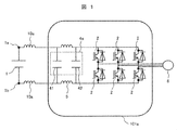
- FIG. 1 is a circuit diagram showing the configuration of a power conversion device according to a first embodiment of the present invention.
- the DC power supply 1 is connected between the input terminals 1a and 1b, and the DC side of the power conversion main circuit configured by the semiconductor switching element 2 is connected to the DC power supply 1. It is connected via a plurality of smoothing capacitors 41 and 42. Further, the AC side of the power conversion main circuit, that is, the output of the power conversion circuit is connected to the load 6.
- the smoothing capacitor 41 has a positive temperature characteristic of electrostatic capacitance.
- the smoothing capacitor 42 connected in parallel to the smoothing capacitor 41 has a negative temperature characteristic of electrostatic capacitance. Therefore, in the present embodiment, the positive and negative values of the amount of change in capacitance of the smoothing capacitor 41 and the smoothing capacitor 42 with temperature change are opposite to each other. As a result, the amounts of change in the capacitances of the smoothing capacitor 41 and the smoothing capacitor 42 cancel each other out, and the temperature fluctuation of the value of the total capacitance of the smoothing capacitor group 4a is suppressed. For example, if the absolute value of each variation is made substantially the same, the total capacitance of the smoothing capacitor group 4a is kept constant even if the temperature fluctuates.
- the plurality of smoothing capacitors 41 and 42 are connected in parallel with each other via the wiring inductance 5 to form a smoothing capacitor group 4 a.
- the smoothing capacitors 41 and 42 constituting the smoothing capacitor group 4a are arranged adjacent to each other.
- the smoothing capacitor group 4a is connected to the DC power supply 1 through the wiring inductance 10a and the input terminals 1a and 1b. Therefore, in the first embodiment, the smoothing capacitor 41 is connected in parallel to the DC power supply through the wiring inductance 10 a among the wiring inductances 5 and 10 a, and parallel to the DC side of the power conversion main circuit through the wiring inductance 5. Connected to Further, the smoothing capacitor 42 is connected in parallel to the DC power supply through the wiring inductance 5 and 10a among the wiring inductances 5 and 10a, and in parallel to the DC side of the power conversion main circuit without the wiring inductance 5 and 10a.
- the value of the wiring inductance 5 is sufficiently smaller than the value of the wiring inductance 10a. That is, the wiring length between the smoothing capacitors 41 and 42 is sufficiently shorter than the wiring length between the smoothing capacitor group 4 a and the DC power supply 1.
- the power conversion main circuit is a three-phase inverter provided with a three-phase full bridge circuit formed of the semiconductor switching element 2, and the load 6 is a three-phase AC load such as a three-phase AC motor.
- the semiconductor switching element 2 an IGBT (Insulated Gate Bipolar Transistor), a MOSFET (Metal Oxide Semiconductor Field Effect Transistor), or the like is applied (in FIG. 1, the IGBT is described).
- one arm of the three-phase full bridge circuit is formed of one semiconductor switching element 2.
- the present invention is not limited to this. Even if a plurality of semiconductor switching elements are connected in series and parallel, good.
- the power conversion device 101a turns DC power supplied from the DC power supply 1 into AC power by turning on / off the semiconductor switching element 2 constituting the power conversion main circuit by switching control such as PWM control (PWM: Pulse Width Modulation). It converts to electric power and outputs this AC power to the load 6. That is, the power conversion device 101a is an inverse converter (inverter). At this time, ripple current flows through the smoothing capacitor group 4, but the magnitude of the ripple current is determined by the capacitance of the smoothing capacitor 41, the capacitance of the smoothing capacitor 42, and the wiring inductance between the smoothing capacitor 41 and the smoothing capacitor 42. 5 depends on LC resonance.
- PWM Pulse Width Modulation
- FIG. 2 shows frequency characteristics of LC resonance.
- the switching frequency of the semiconductor switching element 2 matches the resonant frequency 118
- a large ripple current flows in the smoothing capacitor group 4a.
- the capacitor temperature rises.
- the smoothing capacitor 41 having a positive temperature characteristic in electrostatic capacitance the electrostatic capacitance is increased.
- the smoothing capacitor 42 having a negative temperature characteristic in electrostatic capacitance reduces the electrostatic capacitance.
- the capacitor current i is represented by the equation (1), where C is a capacitance and V is a capacitor voltage.
- dV / dt represents the time rate of change of the capacitor voltage.
- the characteristics of the smoothing capacitor 41 and the smoothing capacitor 42 are made different as described below.
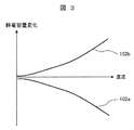
- FIG. 3 shows temperature characteristics of the capacitances of the smoothing capacitor 41 and the smoothing capacitor 42.
- the vertical axis represents the change in capacitance, and the horizontal axis represents temperature.
- the capacitance of the smoothing capacitor 41 has a positive temperature characteristic 102b, and the capacitance of the smoothing capacitor 42 has a negative temperature characteristic 102a.
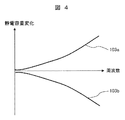
- FIG. 4 shows frequency characteristics of the capacitances of the smoothing capacitor 41 and the smoothing capacitor 42.
- the vertical axis indicates the change in capacitance, and the horizontal axis indicates the frequency.
- the capacitance of the smoothing capacitor 41 has a negative frequency characteristic 103b, and the capacitance of the smoothing capacitor 42 shows a positive frequency characteristic 103a.
- the capacitance of the smoothing capacitor 41 has positive temperature characteristics and negative frequency characteristics
- the increase in capacitance due to temperature rise is due to the negative frequency characteristics at high frequencies close to the resonance frequency. It is offset by the decrease in capacitance. For this reason, the increase in the current flowing to the smoothing capacitor 41 is suppressed.
- the capacitance of the smoothing capacitor 42 has negative temperature characteristics and a positive frequency
- the decrease in the capacitance due to temperature rise is caused by the positive frequency characteristics at high frequencies close to the resonance frequency. Offset by an increase in For this reason, a reduction in the current flowing to the smoothing capacitor 41 is suppressed. For this reason, the increase in current unbalance between the smoothing capacitor 41 and the smoothing capacitor 42 is prevented.
- film capacitors having different dielectric film materials are applied as the smoothing capacitors having different temperature characteristics and frequency characteristics of capacitance.
- the dielectric film material is appropriately selected from polypropylene, polyethylene terephthalate, polyphenylene sulfide, polyethylene, polyester and the like.
- a film capacitor using polypropylene as a dielectric film material is applied as the smoothing capacitor 41
- a film capacitor using polyethylene terephthalate as a dielectric film material is applied as the smoothing capacitor 42.
- An electrolytic capacitor, a ceramic capacitor, or the like may be applied as long as it is a capacitor that can obtain temperature characteristics and frequency characteristics of positive and negative electrostatic capacitances as well as the film capacitors.
- a film capacitor has a relatively high withstand voltage and low loss. Such a feature is suitable for a power converter.
- film capacitors have temperature characteristics of capacitance. Therefore, the first embodiment is particularly suitable when a film capacitor is applied (the same applies to each embodiment and each modification described later).
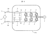
- FIG. 5 shows a power converter according to a modification of the first embodiment.
- the value of the inductance of the wiring inductance 5 is sufficiently smaller than the value of the wiring inductance 10b (corresponding to the wiring inductance 10a in FIG. 1). As well).
- the power conversion device 101b (FIG. 5) has the same circuit configuration as that of the first embodiment (FIG. 1), but operates differently as the first embodiment and operates as a forward converter.
- an AC power supply 7 is connected to the AC side of the power conversion main circuit composed of the semiconductor switching element 2, and the DC side of the power conversion main circuit is through the smoothing capacitor group 4a and the wiring inductance 10b. Load 6 is connected.
- the power conversion device 101 b converts AC power supplied from the AC power supply 7 into DC power, and outputs the DC power to the load 6.
- AC power supply 7 is a three-phase AC power supply
- load 6 is a DC load.
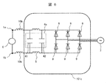
- FIG. 6 shows a power converter according to another modification of the first embodiment. Hereinafter, differences from the first embodiment will be described.
- the power conversion main circuit is a rectifier provided with a three-phase full bridge circuit consisting of diodes 9. Therefore, the power conversion device 101 c operates as a forward converter, converts alternating current power supplied from the alternating current power supply 7 into direct current power, and outputs the direct current power to the load 6.
- AC power supply 7 is a three-phase AC power supply
- load 6 is a DC load.
- Embodiment 2 of the present invention will be described, but mainly points different from Embodiment 1 will be described.
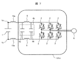
- FIG. 7 is a circuit diagram showing a configuration of a power conversion device according to a second embodiment of the present invention.
- the smoothing capacitor 43 and the smoothing capacitor 44 are connected in parallel via the wiring inductance 5.
- the smoothing capacitor 43 has positive temperature characteristics in terms of electrostatic capacitance
- the smoothing capacitor 44 has negative temperature characteristics in terms of electrostatic capacitance.
- the temperature change of the total capacitance is suppressed as the smoothing capacitor group 4b.
- the temperature characteristics of the equivalent series resistance of the smoothing capacitors 43 and 44 are different from each other.
- the circuit configuration of the power conversion device 101d other than the smoothing capacitor group 4b is the same as that of the first embodiment (FIG. 1).
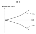
- FIG. 8 shows the temperature characteristics of the equivalent series resistance of the smoothing capacitor 43 and the smoothing capacitor 44.
- the vertical axis represents the change in equivalent series resistance, and the horizontal axis represents temperature.
- the equivalent series resistance of the smoothing capacitor 43 has a positive temperature characteristic 102c
- the equivalent series resistance of the smoothing capacitor 44 has a negative temperature characteristic 103c.
- the equivalent series resistance has a positive temperature characteristic
- the equivalent series resistance increases as the temperature rises. For this reason, the increase in the current flowing to the smoothing capacitor 43 is suppressed.
- the equivalent series resistance has a negative temperature characteristic
- the equivalent series resistance decreases as the temperature rises. For this reason, the decrease in the current flowing to the smoothing capacitor 44 is suppressed. Therefore, an increase in the current unbalance between the smoothing capacitor 43 and the smoothing capacitor 42 due to the difference between the positive and negative temperature characteristics of the capacitance is prevented.
- the smoothing capacitors 43 and 44 film capacitors having different dielectric film materials are applied as the smoothing capacitors having different temperature characteristics of capacitance and temperature characteristics of equivalent series resistance.
- the dielectric film material is appropriately selected from polypropylene, polyethylene terephthalate, polyphenylene sulfide, polyethylene and the like.
- a film capacitor using polypropylene as a dielectric film material is applied as the smoothing capacitor 43
- a film capacitor using polyethylene terephthalate as a dielectric film material is applied as the smoothing capacitor 44.
- electrolytic capacitors, ceramic capacitors, etc. may be applied as long as they are capacitors that can obtain positive / negative temperature characteristics of electrostatic capacitance and positive / negative temperature characteristics of equivalent series resistance.
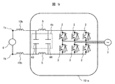
- FIG. 9 shows a power converter according to a modification of the second embodiment.
- the present modification corresponds to the modification (FIG. 5) of the first embodiment described above.
- the power converter 101e (FIG. 9) has the same circuit configuration as that of the second embodiment (FIG. 7), but operates differently as the forward converter in the second embodiment. .
- FIG. 10 shows a power converter which is another modification of the second embodiment.
- the present modification corresponds to another modification (FIG. 6) of the first embodiment described above.
- the power conversion main circuit is a rectifier provided with a three-phase full bridge circuit consisting of diodes 9. Therefore, the power conversion device 101 f operates as a forward converter.
- smoothing capacitor group 4b in the modification of the second embodiment shown in FIGS. 9 and 10 has the same configuration as that of the second embodiment, the same effect as the second embodiment described above can be obtained also in these modifications. .
- Embodiment 2 of the present invention will be described, but mainly points different from Embodiments 1 and 2 will be described.
- FIG. 11 is a circuit diagram showing a configuration of a power conversion device according to a third embodiment of the present invention.
- the circuit configuration including the power conversion device 101g is the same as the first embodiment (FIG. 1) and the second embodiment (FIG. 7), but in the third embodiment, the smoothing capacitor group 4b and A voltage sensor 8 is connected between DC terminals 1 c and 1 d between the DC side of the power conversion main circuit consisting of the semiconductor switching element 2.
- the smoothing capacitor 45 in the smoothing capacitor group 4c has positive temperature characteristics and negative frequency characteristics in terms of electrostatic capacitance, as with the smoothing capacitor 41 in the first embodiment (FIG. 1). Further, the smoothing capacitor 46 in the smoothing capacitor group 4c has a negative temperature characteristic and a positive frequency characteristic in electrostatic capacitance, as with the smoothing capacitor 42 in the first embodiment (FIG. 1).
- the detection value of the voltage sensor 8 is used to control AC power output from the power conversion device 101g in a control device (not shown). Furthermore, in the third embodiment, as described later, when occurrence of current unbalance of the smoothing capacitors 45 and 46 is detected based on the detection value of the voltage sensor 8, the carrier frequency used for PWM control is increased. Thereby, the impedance of each smoothing capacitor is increased, and the magnitude of the ripple current flowing in each smoothing capacitor is suppressed. Therefore, excessive current unbalance can be prevented, and the life deterioration of each smoothing capacitor can be prevented.
- the voltage sensor 8 detects the DC voltage input voltage of the power conversion device 101g, that is, the voltage value of the smoothing capacitor group 4c.
- the control device (not shown) detects the magnitude of the voltage change of the smoothing capacitor group 4 c based on the voltage value detected by the voltage sensor 8.
- the magnitude of the voltage change of the smoothing capacitor group 4c indicates the speed of charging / discharging of the smoothing capacitor group 4c, and as shown by the above-mentioned equation (1), the magnitude of the total capacitance of the smoothing capacitor group 4c Change depending on In particular, when the total capacitance of the smoothing capacitor group 4c decreases and the ripple removal performance of the smoothing capacitor group 4c decreases, charging / discharging is accelerated, and the magnitude of the voltage change increases.
- control device determines whether or not the detected value of the magnitude of the voltage change of the smoothing capacitor group 4c exceeds the preset threshold value. It is determined whether or not the total capacitance of the capacitor is reduced, that is, whether the current imbalance of the smoothing capacitors 45 and 46 is generated as the temperature rises.
- FIG. 12 shows a carrier and a modulation wave used for PWM control (PWM: Pulse Width Modulation) of the power conversion device in the third embodiment.
- PWM Pulse Width Modulation
- a modulated wave 116 (voltage command) having a fundamental frequency as shown in FIG. 12 and a triangular wave carrier 117 having a frequency sufficiently higher than that of the modulated wave 116 and having a high frequency corresponding to the switching frequency of the semiconductor switching element 2
- a PWM pulse serving as a switching pattern of the semiconductor switching element 2 is generated.
- the PWM control in the third embodiment is a known technique, and further detailed description is omitted.
- FIG. 13 shows an equivalent circuit of a capacitor.
- the capacitor is represented by a series connection circuit of an internal inductance 113, a capacitance 114, and an equivalent series resistance 115 (ESR: Equivalent Series Resistance).
- ESR Equivalent Series Resistance
- the size of the internal inductance 113 mainly depends on the configuration of the metal conductor such as the internal electrode and the lead of the capacitor, so there is little temperature dependency and frequency dependency.
- the size of the capacitance 114 depends on the characteristics of the dielectric, it has frequency characteristics and temperature characteristics as in the third embodiment and the first and second embodiments.
- the equivalent series resistance 115 is composed of the electrical resistance components of the dielectric and the metal conductor, it has frequency characteristics and temperature characteristics as described in the second embodiment.
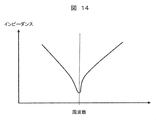
- FIG. 14 shows an example of the frequency characteristic of the impedance of the capacitor.
- the impedance Z of the capacitor is expressed by equation (2) from the equivalent circuit shown in FIG.
- R, L, and C indicate the equivalent series resistance 115, the internal inductance 113, and the electrostatic capacitance 114, respectively.
- ⁇ indicates an angular frequency.
- FIG. 14 shows an example of the relationship between the magnitude of Z and ⁇ expressed by the equation (2), that is, the RLC series resonance characteristic. Therefore, in the third embodiment, the impedances of the smoothing capacitors 45 and 46 have such resonance characteristics.
- the impedance increases as the frequency moves away from the resonance point.
- the reactance component by the electrostatic capacitance 114 is dominant on the low frequency side, and the reactance component by the internal inductance 113 is dominant on the high frequency side. Therefore, on the low frequency side, the difference in capacitance 114 of the capacitor has a large influence on the impedance. Therefore, when the capacitance of each smoothing capacitor varies as the temperature rises, the impedance of the smoothing capacitor is large even if the carrier frequency is lowered to increase the impedance of the smoothing capacitor. Because of variations, it is difficult to prevent current imbalance.
- the difference in the internal inductance 113 of the capacitor has a large influence on the impedance.
- the temperature dependency of the internal inductance 113 is small. Therefore, when variations occur in the capacitance of each smoothing capacitor as the temperature rises, the carrier frequency is made higher than usual to increase the size of the impedance of each smoothing capacitor, whereby the current flows in each smoothing capacitor. Since the magnitude of the ripple current is suppressed, it is possible to prevent excessive current unbalance.
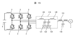
- FIG. 15 is a circuit diagram showing a configuration of a power conversion device that is Embodiment 4 of the present invention.
- the power conversion device of the third embodiment is connected to an AC power system.
- the AC power system is indicated by the system power source 131 and the system inductance 131 and the parasitic capacitance 132 between the AC power source 7 and the power conversion device.
- the power conversion device of the present embodiment includes a power conversion main circuit configured of the semiconductor switching element 2 as in the first to third embodiments (FIGS. 1, 7 and 11).
- the direct current side of the power conversion circuit is connected to a storage device 4 for storing direct current power.
- the AC side of the power conversion main circuit is connected to an AC power system via a harmonic filter 119.
- the power conversion main circuit converts the AC power from the AC power system into DC power and stores the power in the power storage device 4 by controlling the semiconductor switching element 2 on and off, and AC powers the DC power from the power storage device 4 Convert to electric power and output to AC power system.
- the superposition of the harmonic current included in the AC power output from the power conversion device on the AC power system is suppressed by the harmonic filter 119.
- the harmonic filter 119 includes an LC filter circuit configured of a reactor connected in series and a filter capacitor connected to a series connection point of the reactors.
- the LC filter circuit includes a reactor 120 connected in series, and capacitors 121 and 122 connected between a series connection point of the reactor 120 and the ground 123.
- the capacitors 121 and 122 are connected in parallel to each other to form a filter capacitor.
- the capacitor 121 in the filter capacitor has positive temperature characteristics and negative frequency characteristics in terms of electrostatic capacitance, as with the smoothing capacitor 41 in the first embodiment (FIG. 1). Further, the capacitor 122 in the filter capacitor has negative temperature characteristics and positive frequency characteristics in terms of electrostatic capacitance, as with the smoothing capacitor 42 in the first embodiment (FIG. 1).
- the filter performance can be maintained against temperature fluctuation, and the life degradation of the harmonic filter due to the current unbalance can be prevented.
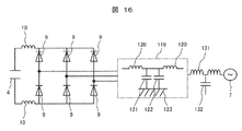
- FIG. 16 shows a power converter which is a modification of the fourth embodiment.
- points different from the fourth embodiment will be described.
- the power conversion main circuit is a rectifier provided with a three-phase full bridge circuit consisting of diodes 9. Accordingly, the power conversion device operates as a forward converter, converts AC power supplied from the power system into DC power, and stores the DC power in the storage device 4.
- the filter capacitor group in this modification has the same configuration as that of the fourth embodiment, the same effect as that of the first embodiment described above can be obtained in this modification as well.
- each of the capacitor 121 and the capacitor 121 described above has a positive temperature characteristic in electrostatic capacitance and a negative temperature dependency in equivalent series resistance and a negative capacitor.
- the effect similar to that of the fourth embodiment can be obtained also as a capacitor having a temperature characteristic and a positive temperature dependency on equivalent series resistance.
- a fifth embodiment of the present invention will next be described, mainly focusing on differences from the first to fourth embodiments.
- FIG. 17 is a circuit diagram showing a configuration of a power conversion device according to a fifth embodiment of the present invention.
- the power conversion device in the fifth embodiment operates as a three-phase inverter as in the first embodiment, but unlike the first embodiment (FIG. 1), the two smoothing capacitor groups 4a are two. It is connected in parallel.
- the smoothing capacitor 41 has positive temperature characteristics and negative frequency characteristics in capacitance
- the smoothing capacitor 42 has negative temperature characteristics in capacitance and It has positive frequency characteristics.
- the total capacitance as the entire smoothing capacitor can be increased by parallel connection of the smoothing capacitor group 4a, and the fluctuation of the total capacitance due to the temperature fluctuation can be suppressed. Further, since the current imbalance of each capacitor can be suppressed, the life deterioration as the whole smoothing capacitor can be suppressed.
- the two smoothing capacitor groups 4 a are connected in parallel to each other via the wiring inductance 5.
- the two smoothing capacitor groups 4a are arranged adjacent to each other, so the four smoothing capacitors in FIG. 17 are arranged adjacent to each other.
- a group of smoothing capacitors (four smoothing capacitors in FIG. 17) constituting two smoothing capacitor groups 4a includes two adjacent smoothing capacitors including smoothing capacitor 41 and smoothing capacitor 42. To be arranged.
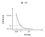
- FIG. 18 shows the relationship between the element life of the capacitor and the operating temperature.
- the element life of the capacitor is reduced by half when the operating temperature is increased by 10.degree.
- the lifetime of the capacitor is greatly influenced by the temperature.
- each smoothing capacitor When a plurality of smoothing capacitors are disposed adjacent to each other as in the fifth embodiment, the operating temperature of each smoothing capacitor affects not only self-heating and ambient temperature, but also the heating of other adjacent smoothing capacitors. Be done. For this reason, when heat generation of a certain smoothing capacitor is increased due to current concentration, not only the temperature of the smoothing capacitor rises but also the temperatures of other adjacent smoothing capacitors. For this reason, there is a possibility that the life deterioration as the whole of a plurality of smoothing capacitors may become large.
- each smoothing capacitor group 4a has a smoothing capacitor 41 having positive temperature characteristics and negative frequency characteristics in electrostatic capacity, and negative temperature characteristics and positive frequency characteristics in electrostatic capacity. Because the smoothing capacitor 42 has the following characteristics, fluctuations in the total capacitance of the plurality of smoothing capacitors as a whole are suppressed with respect to temperature fluctuations, and current concentration due to current imbalance and heat generation due to it are increased. Can be suppressed. Therefore, the life deterioration of the plurality of smoothing capacitors as a whole can be suppressed.
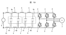
- FIG. 19 shows a power converter which is a modification of the fifth embodiment. Hereinafter, points different from the fifth embodiment will be described.
- the power conversion device (FIG. 19) has the same circuit configuration as that of the first embodiment (FIG. 1), but operates differently as the 19th embodiment as a forward converter.
- an AC power supply 7 is connected to the AC side of the power conversion main circuit formed of the semiconductor switching element 2, and two smoothing capacitor groups 4a and wiring inductance are connected to the DC side of the power conversion main circuit.
- the load 6 is connected via 10b.
- the power conversion device of this modification converts AC power supplied from the AC power supply 7 into DC power, and outputs this DC power to the load 6.
- AC power supply 7 is a three-phase AC power supply
- load 6 is a DC load.
- each smoothing capacitor group 4a in this modification has the same configuration as that of the fifth embodiment, the same effect as that of the above-mentioned fifth embodiment can be obtained also in this modification.
- FIG. 20 shows a power converter which is another modification of the fifth embodiment.
- points different from the fifth embodiment will be described.
- the power conversion main circuit is a rectifier provided with a three-phase full bridge circuit consisting of diodes 9. Therefore, the power conversion device of the present modification operates as a forward converter, converts AC power supplied from the AC power supply 7 into DC power, and outputs the DC power to the load 6.
- AC power supply 7 is a three-phase AC power supply
- load 6 is a DC load.
- each smoothing capacitor group 4a in this modification has the same configuration as that of the first embodiment, the same effect as that of the fifth embodiment described above can be obtained in this modification as well.
- the smoothing capacitor 41 and the smoothing capacitor 42 described above are respectively a capacitor having a positive temperature characteristic in electrostatic capacitance and a negative temperature dependence in equivalent series resistance.
- the effect similar to that of the fifth embodiment can be obtained also as a capacitor having negative temperature characteristics and positive temperature dependency in equivalent series resistance.
- the present invention is not limited to the embodiments described above, but includes various modifications.
- the embodiments described above are described in detail in order to explain the present invention in an easy-to-understand manner, and are not necessarily limited to those having all the configurations described.
- the number of paralleling smoothing capacitors and the number of paralleling smoothing capacitor groups may be any plural numbers.
- the voltage may be increased by configuring the above-mentioned smoothing capacitor by connecting a plurality of single capacitors in series.
Landscapes
- Engineering & Computer Science (AREA)
- Power Engineering (AREA)
- Inverter Devices (AREA)
Abstract
La présente invention concerne un dispositif de conversion d'énergie permettant de supprimer une fluctuation de capacité de condensateur due à la température et de supprimer un déséquilibre de courant entre des condensateurs. Ce dispositif de conversion d'énergie (101a) est pourvu d'un circuit principal de conversion d'énergie, et d'une pluralité de condensateurs (41, 42) qui sont connectés au côté d'entrée ou de sortie du circuit de conversion d'énergie et qui absorbent les courants harmoniques. La pluralité de condensateurs comprend un premier condensateur (41) et un second condensateur (42) qui sont connectés en parallèle l'un avec l'autre. Le premier condensateur (41) présente une caractéristique de température positive en capacité, et le second condensateur (42) présente une caractéristique de température négative en capacité. De plus, le premier condensateur (41) présente une caractéristique de fréquence négative en capacité, et le second condensateur (42) présente une caractéristique de fréquence positive en capacité. En variante, le premier condensateur (41) présente une caractéristique de température négative dans une résistance série équivalente, et le second condensateur (42) présente une caractéristique de température positive dans une résistance série équivalente.
Priority Applications (1)
| Application Number | Priority Date | Filing Date | Title |
|---|---|---|---|
| PCT/JP2017/041566 WO2019097699A1 (fr) | 2017-11-17 | 2017-11-17 | Dispositif de conversion d'énergie |
Applications Claiming Priority (1)
| Application Number | Priority Date | Filing Date | Title |
|---|---|---|---|
| PCT/JP2017/041566 WO2019097699A1 (fr) | 2017-11-17 | 2017-11-17 | Dispositif de conversion d'énergie |
Publications (1)
| Publication Number | Publication Date |
|---|---|
| WO2019097699A1 true WO2019097699A1 (fr) | 2019-05-23 |
Family
ID=66539468
Family Applications (1)
| Application Number | Title | Priority Date | Filing Date |
|---|---|---|---|
| PCT/JP2017/041566 Ceased WO2019097699A1 (fr) | 2017-11-17 | 2017-11-17 | Dispositif de conversion d'énergie |
Country Status (1)
| Country | Link |
|---|---|
| WO (1) | WO2019097699A1 (fr) |
Cited By (4)
| Publication number | Priority date | Publication date | Assignee | Title |
|---|---|---|---|---|
| CN115242066A (zh) * | 2022-09-15 | 2022-10-25 | 荣耀终端有限公司 | 一种电源电路及其产品 |
| WO2023136181A1 (fr) * | 2022-01-17 | 2023-07-20 | 株式会社村田製作所 | Dispositif de conversion de puissance, dispositif capacitif, procédé de commande, et programme informatique |
| EP4380032A4 (fr) * | 2021-07-28 | 2024-08-21 | Mitsubishi Electric Corporation | Dispositif de conversion de puissance et climatiseur |
| JP2025512526A (ja) * | 2022-07-12 | 2025-04-17 | シェンジェン コア メディカル テクノロジー カンパニー リミテッド | 無線充電整流回路、無線充電装置及び心室補助装置 |
Citations (3)
| Publication number | Priority date | Publication date | Assignee | Title |
|---|---|---|---|---|
| JPS6252916A (ja) * | 1985-09-02 | 1987-03-07 | 株式会社東芝 | 放電灯点灯装置 |
| JP2008061472A (ja) * | 2006-09-04 | 2008-03-13 | Matsushita Electric Ind Co Ltd | 直流電圧変換装置 |
| JP2010226606A (ja) * | 2009-03-25 | 2010-10-07 | Denso Corp | 負荷制御装置及びコンデンサのインピーダンス調整方法 |
-
2017
- 2017-11-17 WO PCT/JP2017/041566 patent/WO2019097699A1/fr not_active Ceased
Patent Citations (3)
| Publication number | Priority date | Publication date | Assignee | Title |
|---|---|---|---|---|
| JPS6252916A (ja) * | 1985-09-02 | 1987-03-07 | 株式会社東芝 | 放電灯点灯装置 |
| JP2008061472A (ja) * | 2006-09-04 | 2008-03-13 | Matsushita Electric Ind Co Ltd | 直流電圧変換装置 |
| JP2010226606A (ja) * | 2009-03-25 | 2010-10-07 | Denso Corp | 負荷制御装置及びコンデンサのインピーダンス調整方法 |
Cited By (7)
| Publication number | Priority date | Publication date | Assignee | Title |
|---|---|---|---|---|
| EP4380032A4 (fr) * | 2021-07-28 | 2024-08-21 | Mitsubishi Electric Corporation | Dispositif de conversion de puissance et climatiseur |
| WO2023136181A1 (fr) * | 2022-01-17 | 2023-07-20 | 株式会社村田製作所 | Dispositif de conversion de puissance, dispositif capacitif, procédé de commande, et programme informatique |
| JPWO2023136181A1 (fr) * | 2022-01-17 | 2023-07-20 | ||
| JP7750308B2 (ja) | 2022-01-17 | 2025-10-07 | 株式会社村田製作所 | 電力変換装置、コンデンサ装置、制御方法およびコンピュータプログラム |
| JP2025512526A (ja) * | 2022-07-12 | 2025-04-17 | シェンジェン コア メディカル テクノロジー カンパニー リミテッド | 無線充電整流回路、無線充電装置及び心室補助装置 |
| CN115242066A (zh) * | 2022-09-15 | 2022-10-25 | 荣耀终端有限公司 | 一种电源电路及其产品 |
| CN115242066B (zh) * | 2022-09-15 | 2023-02-07 | 荣耀终端有限公司 | 一种电源电路及其产品 |
Similar Documents
| Publication | Publication Date | Title |
|---|---|---|
| JP5872494B2 (ja) | 車両用電力変換装置 | |
| KR100337035B1 (ko) | 전력용 반도체 스위칭 소자의 직렬구동을 위한 수동형보조회로 | |
| EP1835609B1 (fr) | Circuit d'alimentation en courant multiphase, appareil d'entrainement, compresseur et climatiseur | |
| US8531850B2 (en) | Capacitor circuit and power conversion circuit including a resonant frequency adjustment element | |
| WO2019097699A1 (fr) | Dispositif de conversion d'énergie | |
| US11863166B2 (en) | Power semiconductor module and power converter | |
| WO2013027819A1 (fr) | Module semi-conducteur | |
| JP5098522B2 (ja) | インバータ装置の設計方法 | |
| CN107070268A (zh) | 电力转换机装置 | |
| EP2509207A2 (fr) | Système de conversion d'alimentation | |
| Konrad et al. | New demands on DC link power capacitors | |
| US10128754B2 (en) | Power conversion apparatus | |
| US11374485B2 (en) | Filter unit and frequency inverter | |
| JP5482211B2 (ja) | 電力変換装置のスナバ回路 | |
| JP4765018B2 (ja) | 電力変換装置 | |
| JP5840514B2 (ja) | 漏れ電流抑制回路 | |
| KR101122067B1 (ko) | 다이오드 클램프형 3-레벨 인버터용 스너버 회로 및 그 과전압 방지방법 | |
| KR102349362B1 (ko) | 전력 변환 장치 | |
| US20140340054A1 (en) | Self-discharging capacitor | |
| JP3722649B2 (ja) | 3レベルインバータ | |
| EP3706304A1 (fr) | Onduleur du type courant | |
| JP6782474B2 (ja) | 熱電変換素子出力制御装置 | |
| WO1998001940A1 (fr) | Convertisseur de puissance | |
| JP6718141B2 (ja) | 電力変換器 | |
| JP7475980B2 (ja) | 電力変換装置、変電所用電源装置および回生電力貯蔵装置 |
Legal Events
| Date | Code | Title | Description |
|---|---|---|---|
| 121 | Ep: the epo has been informed by wipo that ep was designated in this application |
Ref document number: 17932053 Country of ref document: EP Kind code of ref document: A1 |
|
| NENP | Non-entry into the national phase |
Ref country code: DE |
|
| 122 | Ep: pct application non-entry in european phase |
Ref document number: 17932053 Country of ref document: EP Kind code of ref document: A1 |
|
| NENP | Non-entry into the national phase |
Ref country code: JP |