WO2019123777A1 - Dispositif à semi-conducteur - Google Patents
Dispositif à semi-conducteur Download PDFInfo
- Publication number
- WO2019123777A1 WO2019123777A1 PCT/JP2018/037389 JP2018037389W WO2019123777A1 WO 2019123777 A1 WO2019123777 A1 WO 2019123777A1 JP 2018037389 W JP2018037389 W JP 2018037389W WO 2019123777 A1 WO2019123777 A1 WO 2019123777A1
- Authority
- WO
- WIPO (PCT)
- Prior art keywords
- semiconductor device
- shield layer
- semiconductor
- semiconductor chip
- spacer
- Prior art date
- Legal status (The legal status is an assumption and is not a legal conclusion. Google has not performed a legal analysis and makes no representation as to the accuracy of the status listed.)
- Ceased
Links
Images


Classifications
-
- H—ELECTRICITY
- H10—SEMICONDUCTOR DEVICES; ELECTRIC SOLID-STATE DEVICES NOT OTHERWISE PROVIDED FOR
- H10W—GENERIC PACKAGES, INTERCONNECTIONS, CONNECTORS OR OTHER CONSTRUCTIONAL DETAILS OF DEVICES COVERED BY CLASS H10
- H10W76/00—Containers; Fillings or auxiliary members therefor; Seals
- H10W76/40—Fillings or auxiliary members in containers, e.g. centering rings
-
- H—ELECTRICITY
- H03—ELECTRONIC CIRCUITRY
- H03B—GENERATION OF OSCILLATIONS, DIRECTLY OR BY FREQUENCY-CHANGING, BY CIRCUITS EMPLOYING ACTIVE ELEMENTS WHICH OPERATE IN A NON-SWITCHING MANNER; GENERATION OF NOISE BY SUCH CIRCUITS
- H03B5/00—Generation of oscillations using amplifier with regenerative feedback from output to input
- H03B5/08—Generation of oscillations using amplifier with regenerative feedback from output to input with frequency-determining element comprising lumped inductance and capacitance
- H03B5/12—Generation of oscillations using amplifier with regenerative feedback from output to input with frequency-determining element comprising lumped inductance and capacitance active element in amplifier being semiconductor device
-
- H—ELECTRICITY
- H10—SEMICONDUCTOR DEVICES; ELECTRIC SOLID-STATE DEVICES NOT OTHERWISE PROVIDED FOR
- H10W—GENERIC PACKAGES, INTERCONNECTIONS, CONNECTORS OR OTHER CONSTRUCTIONAL DETAILS OF DEVICES COVERED BY CLASS H10
- H10W42/00—Arrangements for protection of devices
- H10W42/20—Arrangements for protection of devices protecting against electromagnetic or particle radiation, e.g. light, X-rays, gamma-rays or electrons
-
- H—ELECTRICITY
- H10—SEMICONDUCTOR DEVICES; ELECTRIC SOLID-STATE DEVICES NOT OTHERWISE PROVIDED FOR
- H10W—GENERIC PACKAGES, INTERCONNECTIONS, CONNECTORS OR OTHER CONSTRUCTIONAL DETAILS OF DEVICES COVERED BY CLASS H10
- H10W90/00—Package configurations
-
- H—ELECTRICITY
- H10—SEMICONDUCTOR DEVICES; ELECTRIC SOLID-STATE DEVICES NOT OTHERWISE PROVIDED FOR
- H10W—GENERIC PACKAGES, INTERCONNECTIONS, CONNECTORS OR OTHER CONSTRUCTIONAL DETAILS OF DEVICES COVERED BY CLASS H10
- H10W42/00—Arrangements for protection of devices
- H10W42/20—Arrangements for protection of devices protecting against electromagnetic or particle radiation, e.g. light, X-rays, gamma-rays or electrons
- H10W42/261—Arrangements for protection of devices protecting against electromagnetic or particle radiation, e.g. light, X-rays, gamma-rays or electrons characterised by their shapes or dispositions
- H10W42/271—Arrangements for protection of devices protecting against electromagnetic or particle radiation, e.g. light, X-rays, gamma-rays or electrons characterised by their shapes or dispositions the arrangements being between stacked chips
-
- H—ELECTRICITY
- H10—SEMICONDUCTOR DEVICES; ELECTRIC SOLID-STATE DEVICES NOT OTHERWISE PROVIDED FOR
- H10W—GENERIC PACKAGES, INTERCONNECTIONS, CONNECTORS OR OTHER CONSTRUCTIONAL DETAILS OF DEVICES COVERED BY CLASS H10
- H10W44/00—Electrical arrangements for controlling or matching impedance
- H10W44/20—Electrical arrangements for controlling or matching impedance at high-frequency [HF] or radio frequency [RF]
-
- H—ELECTRICITY
- H10—SEMICONDUCTOR DEVICES; ELECTRIC SOLID-STATE DEVICES NOT OTHERWISE PROVIDED FOR
- H10W—GENERIC PACKAGES, INTERCONNECTIONS, CONNECTORS OR OTHER CONSTRUCTIONAL DETAILS OF DEVICES COVERED BY CLASS H10
- H10W72/00—Interconnections or connectors in packages
- H10W72/851—Dispositions of multiple connectors or interconnections
- H10W72/853—On the same surface
- H10W72/865—Die-attach connectors and bond wires
-
- H—ELECTRICITY
- H10—SEMICONDUCTOR DEVICES; ELECTRIC SOLID-STATE DEVICES NOT OTHERWISE PROVIDED FOR
- H10W—GENERIC PACKAGES, INTERCONNECTIONS, CONNECTORS OR OTHER CONSTRUCTIONAL DETAILS OF DEVICES COVERED BY CLASS H10
- H10W72/00—Interconnections or connectors in packages
- H10W72/851—Dispositions of multiple connectors or interconnections
- H10W72/874—On different surfaces
- H10W72/877—Bump connectors and die-attach connectors
-
- H—ELECTRICITY
- H10—SEMICONDUCTOR DEVICES; ELECTRIC SOLID-STATE DEVICES NOT OTHERWISE PROVIDED FOR
- H10W—GENERIC PACKAGES, INTERCONNECTIONS, CONNECTORS OR OTHER CONSTRUCTIONAL DETAILS OF DEVICES COVERED BY CLASS H10
- H10W72/00—Interconnections or connectors in packages
- H10W72/851—Dispositions of multiple connectors or interconnections
- H10W72/874—On different surfaces
- H10W72/884—Die-attach connectors and bond wires
-
- H—ELECTRICITY
- H10—SEMICONDUCTOR DEVICES; ELECTRIC SOLID-STATE DEVICES NOT OTHERWISE PROVIDED FOR
- H10W—GENERIC PACKAGES, INTERCONNECTIONS, CONNECTORS OR OTHER CONSTRUCTIONAL DETAILS OF DEVICES COVERED BY CLASS H10
- H10W74/00—Encapsulations, e.g. protective coatings
- H10W74/10—Encapsulations, e.g. protective coatings characterised by their shape or disposition
- H10W74/111—Encapsulations, e.g. protective coatings characterised by their shape or disposition the semiconductor body being completely enclosed
- H10W74/114—Encapsulations, e.g. protective coatings characterised by their shape or disposition the semiconductor body being completely enclosed by a substrate and the encapsulations
-
- H—ELECTRICITY
- H10—SEMICONDUCTOR DEVICES; ELECTRIC SOLID-STATE DEVICES NOT OTHERWISE PROVIDED FOR
- H10W—GENERIC PACKAGES, INTERCONNECTIONS, CONNECTORS OR OTHER CONSTRUCTIONAL DETAILS OF DEVICES COVERED BY CLASS H10
- H10W90/00—Package configurations
- H10W90/20—Configurations of stacked chips
- H10W90/231—Configurations of stacked chips the stacked chips being on both top and bottom sides of an auxiliary carrier having no electrical connection structure
-
- H—ELECTRICITY
- H10—SEMICONDUCTOR DEVICES; ELECTRIC SOLID-STATE DEVICES NOT OTHERWISE PROVIDED FOR
- H10W—GENERIC PACKAGES, INTERCONNECTIONS, CONNECTORS OR OTHER CONSTRUCTIONAL DETAILS OF DEVICES COVERED BY CLASS H10
- H10W90/00—Package configurations
- H10W90/701—Package configurations characterised by the relative positions of pads or connectors relative to package parts
- H10W90/721—Package configurations characterised by the relative positions of pads or connectors relative to package parts of bump connectors
- H10W90/724—Package configurations characterised by the relative positions of pads or connectors relative to package parts of bump connectors between a chip and a stacked insulating package substrate, interposer or RDL
-
- H—ELECTRICITY
- H10—SEMICONDUCTOR DEVICES; ELECTRIC SOLID-STATE DEVICES NOT OTHERWISE PROVIDED FOR
- H10W—GENERIC PACKAGES, INTERCONNECTIONS, CONNECTORS OR OTHER CONSTRUCTIONAL DETAILS OF DEVICES COVERED BY CLASS H10
- H10W90/00—Package configurations
- H10W90/701—Package configurations characterised by the relative positions of pads or connectors relative to package parts
- H10W90/731—Package configurations characterised by the relative positions of pads or connectors relative to package parts of die-attach connectors
- H10W90/734—Package configurations characterised by the relative positions of pads or connectors relative to package parts of die-attach connectors between a chip and a stacked insulating package substrate, interposer or RDL
-
- H—ELECTRICITY
- H10—SEMICONDUCTOR DEVICES; ELECTRIC SOLID-STATE DEVICES NOT OTHERWISE PROVIDED FOR
- H10W—GENERIC PACKAGES, INTERCONNECTIONS, CONNECTORS OR OTHER CONSTRUCTIONAL DETAILS OF DEVICES COVERED BY CLASS H10
- H10W90/00—Package configurations
- H10W90/701—Package configurations characterised by the relative positions of pads or connectors relative to package parts
- H10W90/731—Package configurations characterised by the relative positions of pads or connectors relative to package parts of die-attach connectors
- H10W90/736—Package configurations characterised by the relative positions of pads or connectors relative to package parts of die-attach connectors between a chip and a stacked lead frame, conducting package substrate or heat sink
-
- H—ELECTRICITY
- H10—SEMICONDUCTOR DEVICES; ELECTRIC SOLID-STATE DEVICES NOT OTHERWISE PROVIDED FOR
- H10W—GENERIC PACKAGES, INTERCONNECTIONS, CONNECTORS OR OTHER CONSTRUCTIONAL DETAILS OF DEVICES COVERED BY CLASS H10
- H10W90/00—Package configurations
- H10W90/701—Package configurations characterised by the relative positions of pads or connectors relative to package parts
- H10W90/751—Package configurations characterised by the relative positions of pads or connectors relative to package parts of bond wires
- H10W90/754—Package configurations characterised by the relative positions of pads or connectors relative to package parts of bond wires between a chip and a stacked insulating package substrate, interposer or RDL
Definitions
- the present technology relates to a semiconductor device that can be applied to, for example, a tuner that receives television broadcasting.
- the PLL circuit is configured by an LC resonant oscillation circuit.
- the tuner unit is configured by each of two vertically stacked semiconductor chips, the position where the coil of the LC resonant oscillation circuit is formed is the same position on each semiconductor chip. Therefore, the magnetic flux generated from the coil of one oscillator crosses the other coil, causing a problem that the oscillation frequency of the other oscillator fluctuates.
- Patent Document 1 proposes a technique of sandwiching two or more spacers having different areas between semiconductor chips as a technique for avoiding deflection in a semiconductor multilayer package.
- Patent Document 1 focuses on prevention of deflection and suppression of voids, and does not suppress electromagnetic coupling between upper and lower semiconductor chips as described above.
- the metal film thickness is thin or when the frequency of the noise source is low, sufficient absorption loss in the metal film of noise can not be obtained, and a sufficient noise suppression effect can not be obtained.
- the metal film is not electrically grounded to the earth, and the shielding effect is limited.
- an object of the present technology is to provide a semiconductor device in which semiconductor chips are arranged vertically stacked, and are not affected by mutual electromagnetic field interference.
- the present technology is a semiconductor device in which a plurality of semiconductor chips are vertically arranged via a spacer, In the semiconductor device, a shield layer having a thickness sufficient to absorb electromagnetic field radiation generated from a generation source of the semiconductor chip is disposed between the semiconductor chips.
- the effect described here is not necessarily limited, and may be any effect or an effect different from them described in the present technology.
- the contents of the present technology are not to be interpreted as being limited by the effects illustrated in the following description.
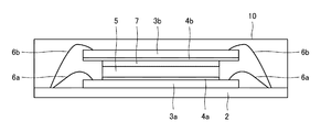
- FIG. 1 is a cross-sectional view of a first embodiment of the present technology.
- FIG. 2 is a schematic diagram used to explain the function of the shield layer.
- FIG. 3 is a cross-sectional view of a second embodiment of the present technology.
- FIG. 4 is a cross-sectional view of a third embodiment of the present technology.
- FIG. 5 is a cross-sectional view of a fourth embodiment of the present technology.
- FIG. 6 is a block diagram of an application example of the present technology.
- FIG. 7 is a cross-sectional view used to explain the conventional semiconductor device.
- FIG. 8 is a schematic diagram used to explain problems of the conventional semiconductor device.
- FIG. 9 is a cross-sectional view showing another example of the conventional semiconductor device.
- the conventional semiconductor device 11A shown in FIG. 7 has two semiconductor chips 13a and 13b of the same configuration disposed on a common substrate 12.
- the semiconductor chips 13a and 13b include various circuits (integrated circuit IC) such as an oscillator, an amplifier, a memory, and a logic.
- integrated circuit IC integrated circuit
- FIG. 7 in the configuration in which the semiconductor chips 13a and 13b are arranged in a plane, there is a problem that the shape (area) of the semiconductor device 11A becomes large.
- semiconductor chips 13a and 13b are vertically stacked.
- the semiconductor chip 13a is disposed on the substrate 12, and the spacer 15 is bonded onto the semiconductor chip 13a by the adhesive 14a.
- the semiconductor chip 13b is bonded onto the spacer 15 by the adhesive 14b.
- the semiconductor chip 13a and the substrate 12 are connected by the wire 16a, and the semiconductor chip 13b and the substrate 12 are connected by the wire 16b.
- FIG. 9 shows a schematic view of the mutual interference due to the magnetic field radiation generated by the circuit.
- the position of the inductor 21a of the LC resonant oscillator included in the semiconductor chip 13a is substantially the same as the position of the inductor 21b of the LC resonant oscillator included in the semiconductor chip 13b.
- An alternating current 22a flows through the inductor 21a, and a magnetic flux 23 is generated by the alternating current 22a.
- the magnetic flux 23 passes through the inductor 21b, an alternating current 22b is generated, which may adversely affect the operation of the oscillator of the semiconductor chip 13b.
- the present technology solves such problems.
- FIG. 1 is a cross-sectional view of a semiconductor device 10 according to the first embodiment.
- the semiconductor chip 3a is fixed on the substrate 2 with an adhesive, silver paste or the like.
- the semiconductor chip 3a includes various circuits such as an oscillator, an amplifier, a memory, and a logic, and for example, a tuner unit of a television receiver is configured.
- Each of the semiconductor chips 3a and 3b is not limited to the configuration including a plurality of ICs and chip components, but a configuration (SoC (System on a Chip)) in which these functions are incorporated on one chip is also possible. .
- SoC System on a Chip
- a spacer 5 is fixed to the upper surface of the semiconductor chip 3a via an adhesive 4a.
- the spacer 5 is formed of, for example, a chip obtained by dicing a silicon wafer.
- the first purpose of providing the spacer 5 is to secure a space for connecting the wire 6a of the substrate 2 to the semiconductor chip 3a. Therefore, the area of the spacer 5 is designed to be smaller than that of the semiconductor chip 3a.
- the second purpose of the spacer 5 is, for example, when the semiconductor chip 3a has an analog circuit such as an oscillator or amplifier or a high-speed logic circuit, and a relatively low resistance substrate is used for the semiconductor chip 3b. This is to ensure insulation so as not to affect the operation of the circuit (for example, LC circuit) of the semiconductor chip 3a. Therefore, the spacer 5 needs to have a sufficiently high resistance and a sufficient thickness as compared with the base material of the semiconductor chip 3a. In the first embodiment, a silicon chip having a resistivity of 100 ⁇ ⁇ cm and a thickness of 200 ⁇ m was used as the spacer 5.
- silicon as well as resistivity> 10 14 ⁇ ⁇ cm of silicon nitride (Si 3 N 4), silicon carbide resistivity of 10 5 ⁇ ⁇ cm (SiC) , resistivity> 10 14 ⁇ ⁇ cm of alumina (Al 2 O 3), resistivity> of 10 13 Omega ⁇ cm zirconia (ZrO 2) and resistivity> of 10 14 Omega ⁇ cm aluminum nitride (AlN) can also be applied to the spacer.
- a shield layer 7 is formed on the top surface of the spacer 5.
- the semiconductor chip 3b is fixed to the upper surface of the shield layer 7 by the adhesive 4b.
- the shield layer 7 is intended to shut off the magnetic flux generated by the inductor of the semiconductor chip 3a.
- the adhesives 4 a and 4 b also need to be made of an insulating material, similarly to the spacer 5.
- the adhesives 4a and 4b may be thin tapes which are sticky on both sides.
- epoxy adhesives were used for the adhesives 4a and 4b. Similar to the above-mentioned adhesives, silicone adhesives, phenolic adhesives and cyanoacrylics are also applicable.
- the shield layer 7 is an aluminum thin film produced by sputtering aluminum on the spacer 5. The same effect can be obtained as long as the metal has a conductivity as high as that of aluminum.
- the shield layer 7 does not have to be grounded.
- the frequency of the electromagnetic field to be particularly prevented is In the case of the high frequency band of several GHz, absorption loss in the shield layer 7 can be expected even if the thickness of the shield layer 7 is about several ⁇ m.
- a metal thin film can be produced by sputtering copper (Cu), nickel (Ni), gold (Au) and silver (Ag) on the spacer 5 respectively.
- a thin film can be produced by forming the above-mentioned metal material by vacuum evaporation, and the same effect can be obtained.
- ⁇ is the skin depth, which is determined by the material of the shield layer 7 and the frequency of the electromagnetic field, and is expressed by the following equation.
- ⁇ ⁇ ( ⁇ ⁇ frequency ⁇ conductivity ⁇ permeability) [m] t is the thickness of the shield layer 7.
- the semiconductor chips 3a and 3b are both tuner units for television broadcast reception, similar signals may be received by the two semiconductor chips 3a and 3b, that is, the frequency of the television.
- An electromagnetic field having a frequency is emitted from the semiconductor chip 3a.
- the semiconductor chips 3a and 3b each include a PLL (Phase Locked Loop) circuit (phase locked circuit) and include a coil sensitive to an external electromagnetic field.
- PLL Phase Locked Loop
- the first embodiment of the present technology described above can suppress magnetic flux generated from the inductor provided in the semiconductor chip 3a from passing through the inductor provided in the semiconductor chip 3b. It is possible to prevent the operation of the oscillator from being adversely affected.
- FIG. 3 is a cross-sectional view showing a semiconductor device 20 according to a second embodiment of the present technology.
- a conductive material is used for the adhesive 4 b without providing the spacer 5 with a shield layer.
- the effect of attenuating the electromagnetic field radiated from the inductor of the semiconductor chip can be obtained by adopting the above-described first embodiment regarding the point of not forming the shield layer 7 and the configuration other than the characteristics of the adhesive 4 b.
- conductive adhesives used for electronic and electrical applications include metal particles such as aluminum (Al), copper (Cu), silver (Ag), gold (Au) and metal plating resin particles. It is a material of an organic-inorganic mixed system in which conductive particles are uniformly dispersed in an organic binder such as epoxy resin.
- FIG. 4 is a cross-sectional view showing a semiconductor device 30 according to a third embodiment of the present technology.
- the area of the shield layer 7 formed on the upper surface of the spacer 5 is limited.
- cracking of the aluminum layer called an aluminum slide may occur. Therefore, in order to avoid the aluminum slide of the aluminum layer, the shield area of the shield layer 7 is minimized, so that the effect of attenuating the electromagnetic field radiated from the inductor of the semiconductor chip can be obtained.
- the shield layer 7 is formed so as to be limited to the area (area and position) which can cover the disturbance source circuit (for example, LC resonant oscillator) of the semiconductor chips 3a and 3b. Since the radiation noise diffuses isotropically, the coverage of the shield layer 7 needs to cover the area obtained by adding the thickness of the spacer from immediately above the disturbance source circuit.
- the configuration other than the coverage of the shield layer 7 is basically the same as that of the first embodiment, so that the effect of attenuating the electromagnetic field radiated from the inductor of the semiconductor chip can be obtained.
- FIG. 5 is a cross-sectional view showing a semiconductor device 40 according to a fourth embodiment of the present technology.
- the lower semiconductor chip 3a is flip-chip mounted, and the wire connection between the substrate 2 and the semiconductor chip 3a is omitted.
- This flip chip mounting is one of the methods of mounting a chip on a mounting substrate, and in the form of an array instead of connecting by wire bonding when electrically connecting the chip surface and the substrate.
- the mounting area can be made smaller compared to wire bonding by connecting by means of projecting terminals called side-by-side bumps.
- the configuration other than the mounting method of the semiconductor chip 3a is basically the same as that of the first embodiment, so that the effect of attenuating the electromagnetic field radiated from the inductor of the semiconductor chip can be obtained.
- the semiconductor device described as the first to fourth embodiments described above can be applied to, for example, a tuner unit of a receiving apparatus that receives digital terrestrial broadcasting or digital satellite broadcasting.
- a tuner unit As a configuration of the tuner unit, there is diversity reception technology which is one of the effective measures against fading. Radio waves in communications are affected by obstacles and reflectors such as buildings and trees, terrain undulations, and cause reflection, diffraction, and scattering. As a result, many radio waves passing through various paths interfere with each other, and the strength of the radio waves changes drastically. This is called fading.
- Diversity technology (Diversity) refers to using the signal of an antenna with excellent radio wave condition for the same radio signal received by multiple antennas, or combining received signals to remove noise.
- the tuner unit TU1 has an RF amplifier 31, a mixer 32, an oscillator 33, and an A / D converter 34 for amplifying the output of the antenna AT1.
- the mixer 32 and the oscillator 33 select a reception channel.
- the tuner unit TU2 has an RF amplifier 41, a mixer 42, an oscillator 43, and an A / D converter 44.
- Each of the tuner units TU1 and TU2 is configured as a semiconductor device according to the present technology described above.
- Oscillators 33 and 43 are configured as LC oscillators, each having a coil.
- the oscillators 33 and 43 constitute a PLL.
- the outputs of the tuner units TU1 and TU2 are supplied to a demodulation and diversity combining unit 45, where OFDM demodulation processing is performed to form a transport stream. Furthermore, in the demodulation and diversity combining unit 45, the outputs of the two tuner units are respectively demodulated and then combined. For example, a selector for selecting the outputs of the two antennas AT1 and AT2 is provided, and the output of one of the antennas is selected by the antenna control signal formed in the demodulation and diversity combining unit 45. In addition to the selection process, a process of combining the outputs of the two antennas AT1 and AT2 at maximum ratio is also possible.
- the spacer 5 is not only this but the material of a high resistance and a low dielectric constant, for example, a glass epoxy board (FR-4)
- FR-4 is an abbreviation of (Flame Retardant Type 4), which is a glass fiber cloth impregnated with an epoxy resin and heat-cured to form a plate, and is a material that has both flame retardancy and low conductivity.
- a glass epoxy board is used as the substrate of this FR4 plate and a copper foil is attached to the board, and is widely used as a material for printed circuit boards.
- the embodiment using aluminum has been described for the shield layer 7, the same effect can be obtained by using a material such as gold or copper that can obtain a conductivity similar to that of aluminum.
- the present technology can also have the following configurations.
- a semiconductor device in which a plurality of semiconductor chips are vertically arranged via spacers A semiconductor device in which a shield layer having a thickness sufficient to absorb electromagnetic field radiation generated from a source of the semiconductor chip is disposed between the semiconductor chips.
- the shield layer is formed in an area and position capable of covering the generation source of the semiconductor chip, and the coverage of the shield layer covers a range obtained by adding the thickness of the spacer from immediately above the generation source (2 The semiconductor device as described in 2.).
- the spacer comprises any one of silicon, alumina, zirconia and aluminum nitride.
- the shield layer is a thin film made of metal.
- the metal thin film of the shield layer contains any one of aluminum, copper, nickel and silver.
- the generation source includes an LC resonator including an inductor and a capacitor.
- the semiconductor chip has an oscillator using the LC resonator.
Landscapes
- Shielding Devices Or Components To Electric Or Magnetic Fields (AREA)
- Semiconductor Integrated Circuits (AREA)
- Physics & Mathematics (AREA)
- Health & Medical Sciences (AREA)
- Electromagnetism (AREA)
- Toxicology (AREA)
Abstract
L'invention concerne un dispositif à semi-conducteur ayant une pluralité de puces semi-conductrices disposées verticalement par l'intermédiaire d'entretoises, une couche de blindage ayant une épaisseur pour absorber suffisamment un rayonnement de champ électromagnétique généré par une source de génération dans les puces semi-conductrices est disposée entre les puces semi-conductrices.
Priority Applications (5)
| Application Number | Priority Date | Filing Date | Title |
|---|---|---|---|
| JP2019560818A JP7179019B2 (ja) | 2017-12-20 | 2018-10-05 | 半導体装置 |
| US16/770,786 US11594519B2 (en) | 2017-12-20 | 2018-10-05 | Semiconductor device |
| DE112018006518.9T DE112018006518T5 (de) | 2017-12-20 | 2018-10-05 | Halbleitervorrichtung |
| CN201880080647.6A CN111480225A (zh) | 2017-12-20 | 2018-10-05 | 半导体装置 |
| JP2022179309A JP7357136B2 (ja) | 2017-12-20 | 2022-11-09 | 半導体装置及びチューナ装置 |
Applications Claiming Priority (2)
| Application Number | Priority Date | Filing Date | Title |
|---|---|---|---|
| JP2017244239 | 2017-12-20 | ||
| JP2017-244239 | 2017-12-20 |
Publications (1)
| Publication Number | Publication Date |
|---|---|
| WO2019123777A1 true WO2019123777A1 (fr) | 2019-06-27 |
Family
ID=66994053
Family Applications (1)
| Application Number | Title | Priority Date | Filing Date |
|---|---|---|---|
| PCT/JP2018/037389 Ceased WO2019123777A1 (fr) | 2017-12-20 | 2018-10-05 | Dispositif à semi-conducteur |
Country Status (5)
| Country | Link |
|---|---|
| US (1) | US11594519B2 (fr) |
| JP (2) | JP7179019B2 (fr) |
| CN (1) | CN111480225A (fr) |
| DE (1) | DE112018006518T5 (fr) |
| WO (1) | WO2019123777A1 (fr) |
Cited By (2)
| Publication number | Priority date | Publication date | Assignee | Title |
|---|---|---|---|---|
| CN112397484A (zh) * | 2019-08-12 | 2021-02-23 | 台湾积体电路制造股份有限公司 | 半导体封装器件及其形成方法 |
| WO2021093408A1 (fr) * | 2019-11-15 | 2021-05-20 | 天津大学 | Duplexeur |
Citations (5)
| Publication number | Priority date | Publication date | Assignee | Title |
|---|---|---|---|---|
| JP2005039596A (ja) * | 2003-07-16 | 2005-02-10 | Sony Corp | 集積化発振回路 |
| JP2005243754A (ja) * | 2004-02-25 | 2005-09-08 | Nec Electronics Corp | 半導体装置 |
| JP2007227414A (ja) * | 2006-02-21 | 2007-09-06 | Seiko Epson Corp | 半導体装置および半導体装置の製造方法 |
| JP2010199286A (ja) * | 2009-02-25 | 2010-09-09 | Elpida Memory Inc | 半導体装置 |
| WO2017122416A1 (fr) * | 2016-01-14 | 2017-07-20 | ソニー株式会社 | Dispositif à semi-conducteur |
Family Cites Families (14)
| Publication number | Priority date | Publication date | Assignee | Title |
|---|---|---|---|---|
| JP3943165B2 (ja) * | 1996-07-26 | 2007-07-11 | ハネウェル・インターナショナル・インコーポレーテッド | チップ・スタックおよびコンデンサ取付の配置 |
| JP2002135669A (ja) | 2000-10-26 | 2002-05-10 | Alps Electric Co Ltd | デジタル放送受信チューナ |
| JP2002261233A (ja) | 2001-03-05 | 2002-09-13 | Sony Corp | 半導体装置及びその製造方法 |
| JP4250038B2 (ja) * | 2003-08-20 | 2009-04-08 | シャープ株式会社 | 半導体集積回路 |
| JP4159960B2 (ja) | 2003-09-30 | 2008-10-01 | シャープ株式会社 | チューナicパッケージおよびデジタル放送受信機用サブアセンブリ |
| JP4161911B2 (ja) | 2004-01-30 | 2008-10-08 | ソニー株式会社 | 集積回路装置 |
| JP2005277356A (ja) | 2004-03-26 | 2005-10-06 | Sanyo Electric Co Ltd | 回路装置 |
| US20080002460A1 (en) * | 2006-03-01 | 2008-01-03 | Tessera, Inc. | Structure and method of making lidded chips |
| US7892858B2 (en) | 2008-03-05 | 2011-02-22 | Stats Chippac, Ltd. | Semiconductor package with stacked semiconductor die each having IPD and method of reducing mutual inductive coupling by providing selectable vertical and lateral separation between IPD |
| JP2012122058A (ja) | 2010-11-18 | 2012-06-28 | Nitto Denko Corp | ダイボンドフィルム、ダイシング・ダイボンドフィルム、ダイボンドフィルムの製造方法、及び、ダイボンドフィルムを有する半導体装置 |
| JP2015109551A (ja) | 2013-12-04 | 2015-06-11 | ソニー株式会社 | チューナ装置 |
| JP6262573B2 (ja) * | 2014-03-07 | 2018-01-17 | ルネサスエレクトロニクス株式会社 | 半導体装置およびその製造方法 |
| US9520356B1 (en) * | 2015-09-09 | 2016-12-13 | Analog Devices, Inc. | Circuit with reduced noise and controlled frequency |
| US10171053B2 (en) * | 2016-05-05 | 2019-01-01 | Skyworks Solutions, Inc. | Apparatus and methods for power amplifiers with an injection-locked oscillator driver stage |
-
2018
- 2018-10-05 WO PCT/JP2018/037389 patent/WO2019123777A1/fr not_active Ceased
- 2018-10-05 US US16/770,786 patent/US11594519B2/en active Active
- 2018-10-05 JP JP2019560818A patent/JP7179019B2/ja active Active
- 2018-10-05 CN CN201880080647.6A patent/CN111480225A/zh active Pending
- 2018-10-05 DE DE112018006518.9T patent/DE112018006518T5/de active Pending
-
2022
- 2022-11-09 JP JP2022179309A patent/JP7357136B2/ja active Active
Patent Citations (5)
| Publication number | Priority date | Publication date | Assignee | Title |
|---|---|---|---|---|
| JP2005039596A (ja) * | 2003-07-16 | 2005-02-10 | Sony Corp | 集積化発振回路 |
| JP2005243754A (ja) * | 2004-02-25 | 2005-09-08 | Nec Electronics Corp | 半導体装置 |
| JP2007227414A (ja) * | 2006-02-21 | 2007-09-06 | Seiko Epson Corp | 半導体装置および半導体装置の製造方法 |
| JP2010199286A (ja) * | 2009-02-25 | 2010-09-09 | Elpida Memory Inc | 半導体装置 |
| WO2017122416A1 (fr) * | 2016-01-14 | 2017-07-20 | ソニー株式会社 | Dispositif à semi-conducteur |
Cited By (3)
| Publication number | Priority date | Publication date | Assignee | Title |
|---|---|---|---|---|
| CN112397484A (zh) * | 2019-08-12 | 2021-02-23 | 台湾积体电路制造股份有限公司 | 半导体封装器件及其形成方法 |
| CN112397484B (zh) * | 2019-08-12 | 2024-09-06 | 台湾积体电路制造股份有限公司 | 半导体封装器件及其形成方法 |
| WO2021093408A1 (fr) * | 2019-11-15 | 2021-05-20 | 天津大学 | Duplexeur |
Also Published As
| Publication number | Publication date |
|---|---|
| US20200388593A1 (en) | 2020-12-10 |
| JP2023015234A (ja) | 2023-01-31 |
| CN111480225A (zh) | 2020-07-31 |
| JP7179019B2 (ja) | 2022-11-28 |
| JP7357136B2 (ja) | 2023-10-05 |
| JPWO2019123777A1 (ja) | 2021-01-21 |
| DE112018006518T5 (de) | 2020-09-03 |
| US11594519B2 (en) | 2023-02-28 |
Similar Documents
| Publication | Publication Date | Title |
|---|---|---|
| CN107258037B (zh) | 无线电子装置 | |
| US10978778B2 (en) | Wafer level package with integrated antennas and means for shielding | |
| US20180205155A1 (en) | Antenna-integrated type communication module and manufacturing method for the same | |
| JP6132692B2 (ja) | アンテナ装置 | |
| US10403540B2 (en) | Integrated circuit | |
| US6753817B2 (en) | Multi-element planar array antenna | |
| JP7357136B2 (ja) | 半導体装置及びチューナ装置 | |
| CN110506367A (zh) | 天线模块和通信装置 | |
| CN102137540A (zh) | 电路板叠层模块和电子装置 | |
| US11177227B2 (en) | Method and apparatus for heat sinking high frequency IC with absorbing material | |
| US9007146B2 (en) | Duplexer | |
| WO2020050341A1 (fr) | Élément d'antenne, module d'antenne et dispositif de communication | |
| US9184492B2 (en) | Radio device | |
| US20210159186A1 (en) | Electronic component module | |
| US20120200782A1 (en) | High frequency module and receiver | |
| JP2010272585A (ja) | フリップチップ実装構造 | |
| JP7266507B2 (ja) | アンテナモジュール及び通信装置 | |
| US20060256017A1 (en) | Antenna module and radio apparatus using the same | |
| CN117355993A (zh) | 双极化天线及包括其的双极化天线组装体 | |
| US20150325534A1 (en) | Semiconductor package for radio communication and method of manufacturing the same | |
| US12193151B2 (en) | High-frequency circuit board and antenna module | |
| JP6365283B2 (ja) | 半導体チップ及び高周波モジュール | |
| JP2010135960A (ja) | 高周波信号受信装置とこれを用いた電子機器 | |
| FI20245818A1 (en) | Electromagnetic absorbing arrangement | |
| JPH0555869A (ja) | マイクロ波給電回路 |
Legal Events
| Date | Code | Title | Description |
|---|---|---|---|
| 121 | Ep: the epo has been informed by wipo that ep was designated in this application |
Ref document number: 18891677 Country of ref document: EP Kind code of ref document: A1 |
|
| ENP | Entry into the national phase |
Ref document number: 2019560818 Country of ref document: JP Kind code of ref document: A |
|
| 122 | Ep: pct application non-entry in european phase |
Ref document number: 18891677 Country of ref document: EP Kind code of ref document: A1 |