WO2019155808A1 - Plateforme de placement de substrat, dispositif de traitement au plasma la comprenant, et procédé de traitement au plasma - Google Patents
Plateforme de placement de substrat, dispositif de traitement au plasma la comprenant, et procédé de traitement au plasma Download PDFInfo
- Publication number
- WO2019155808A1 WO2019155808A1 PCT/JP2019/000283 JP2019000283W WO2019155808A1 WO 2019155808 A1 WO2019155808 A1 WO 2019155808A1 JP 2019000283 W JP2019000283 W JP 2019000283W WO 2019155808 A1 WO2019155808 A1 WO 2019155808A1
- Authority
- WO
- WIPO (PCT)
- Prior art keywords
- substrate
- electrostatic chuck
- cooling jacket
- mounting table
- annular cover
- Prior art date
- Legal status (The legal status is an assumption and is not a legal conclusion. Google has not performed a legal analysis and makes no representation as to the accuracy of the status listed.)
- Ceased
Links
Images




Classifications
-
- H—ELECTRICITY
- H10—SEMICONDUCTOR DEVICES; ELECTRIC SOLID-STATE DEVICES NOT OTHERWISE PROVIDED FOR
- H10P—GENERIC PROCESSES OR APPARATUS FOR THE MANUFACTURE OR TREATMENT OF DEVICES COVERED BY CLASS H10
- H10P72/00—Handling or holding of wafers, substrates or devices during manufacture or treatment thereof
- H10P72/04—Apparatus for manufacture or treatment
- H10P72/0431—Apparatus for thermal treatment
- H10P72/0432—Apparatus for thermal treatment mainly by conduction
-
- H—ELECTRICITY
- H10—SEMICONDUCTOR DEVICES; ELECTRIC SOLID-STATE DEVICES NOT OTHERWISE PROVIDED FOR
- H10P—GENERIC PROCESSES OR APPARATUS FOR THE MANUFACTURE OR TREATMENT OF DEVICES COVERED BY CLASS H10
- H10P72/00—Handling or holding of wafers, substrates or devices during manufacture or treatment thereof
- H10P72/70—Handling or holding of wafers, substrates or devices during manufacture or treatment thereof for supporting or gripping
- H10P72/72—Handling or holding of wafers, substrates or devices during manufacture or treatment thereof for supporting or gripping using electrostatic chucks
- H10P72/722—Details of electrostatic chucks
-
- B—PERFORMING OPERATIONS; TRANSPORTING
- B23—MACHINE TOOLS; METAL-WORKING NOT OTHERWISE PROVIDED FOR
- B23Q—DETAILS, COMPONENTS, OR ACCESSORIES FOR MACHINE TOOLS, e.g. ARRANGEMENTS FOR COPYING OR CONTROLLING; MACHINE TOOLS IN GENERAL CHARACTERISED BY THE CONSTRUCTION OF PARTICULAR DETAILS OR COMPONENTS; COMBINATIONS OR ASSOCIATIONS OF METAL-WORKING MACHINES, NOT DIRECTED TO A PARTICULAR RESULT
- B23Q3/00—Devices holding, supporting, or positioning work or tools, of a kind normally removable from the machine
- B23Q3/15—Devices for holding work using magnetic or electric force acting directly on the work
-
- C—CHEMISTRY; METALLURGY
- C23—COATING METALLIC MATERIAL; COATING MATERIAL WITH METALLIC MATERIAL; CHEMICAL SURFACE TREATMENT; DIFFUSION TREATMENT OF METALLIC MATERIAL; COATING BY VACUUM EVAPORATION, BY SPUTTERING, BY ION IMPLANTATION OR BY CHEMICAL VAPOUR DEPOSITION, IN GENERAL; INHIBITING CORROSION OF METALLIC MATERIAL OR INCRUSTATION IN GENERAL
- C23C—COATING METALLIC MATERIAL; COATING MATERIAL WITH METALLIC MATERIAL; SURFACE TREATMENT OF METALLIC MATERIAL BY DIFFUSION INTO THE SURFACE, BY CHEMICAL CONVERSION OR SUBSTITUTION; COATING BY VACUUM EVAPORATION, BY SPUTTERING, BY ION IMPLANTATION OR BY CHEMICAL VAPOUR DEPOSITION, IN GENERAL
- C23C16/00—Chemical coating by decomposition of gaseous compounds, without leaving reaction products of surface material in the coating, i.e. chemical vapour deposition [CVD] processes
- C23C16/44—Chemical coating by decomposition of gaseous compounds, without leaving reaction products of surface material in the coating, i.e. chemical vapour deposition [CVD] processes characterised by the method of coating
- C23C16/458—Chemical coating by decomposition of gaseous compounds, without leaving reaction products of surface material in the coating, i.e. chemical vapour deposition [CVD] processes characterised by the method of coating characterised by the method used for supporting substrates in the reaction chamber
- C23C16/4582—Rigid and flat substrates, e.g. plates or discs
- C23C16/4583—Rigid and flat substrates, e.g. plates or discs the substrate being supported substantially horizontally
- C23C16/4586—Elements in the interior of the support, e.g. electrodes, heating or cooling devices
-
- H—ELECTRICITY
- H01—ELECTRIC ELEMENTS
- H01J—ELECTRIC DISCHARGE TUBES OR DISCHARGE LAMPS
- H01J37/00—Discharge tubes with provision for introducing objects or material to be exposed to the discharge, e.g. for the purpose of examination or processing thereof
- H01J37/32—Gas-filled discharge tubes
- H01J37/32431—Constructional details of the reactor
- H01J37/32623—Mechanical discharge control means
- H01J37/32642—Focus rings
-
- H—ELECTRICITY
- H01—ELECTRIC ELEMENTS
- H01J—ELECTRIC DISCHARGE TUBES OR DISCHARGE LAMPS
- H01J37/00—Discharge tubes with provision for introducing objects or material to be exposed to the discharge, e.g. for the purpose of examination or processing thereof
- H01J37/32—Gas-filled discharge tubes
- H01J37/32431—Constructional details of the reactor
- H01J37/32715—Workpiece holder
- H01J37/32724—Temperature
-
- H—ELECTRICITY
- H02—GENERATION; CONVERSION OR DISTRIBUTION OF ELECTRIC POWER
- H02N—ELECTRIC MACHINES NOT OTHERWISE PROVIDED FOR
- H02N13/00—Clutches or holding devices using electrostatic attraction, e.g. using Johnson-Rahbek effect
-
- H—ELECTRICITY
- H10—SEMICONDUCTOR DEVICES; ELECTRIC SOLID-STATE DEVICES NOT OTHERWISE PROVIDED FOR
- H10P—GENERIC PROCESSES OR APPARATUS FOR THE MANUFACTURE OR TREATMENT OF DEVICES COVERED BY CLASS H10
- H10P72/00—Handling or holding of wafers, substrates or devices during manufacture or treatment thereof
- H10P72/04—Apparatus for manufacture or treatment
- H10P72/0402—Apparatus for fluid treatment
- H10P72/0418—Apparatus for fluid treatment for etching
- H10P72/0421—Apparatus for fluid treatment for etching for drying etching
-
- H—ELECTRICITY
- H10—SEMICONDUCTOR DEVICES; ELECTRIC SOLID-STATE DEVICES NOT OTHERWISE PROVIDED FOR
- H10P—GENERIC PROCESSES OR APPARATUS FOR THE MANUFACTURE OR TREATMENT OF DEVICES COVERED BY CLASS H10
- H10P72/00—Handling or holding of wafers, substrates or devices during manufacture or treatment thereof
- H10P72/04—Apparatus for manufacture or treatment
- H10P72/0431—Apparatus for thermal treatment
- H10P72/0434—Apparatus for thermal treatment mainly by convection
-
- H—ELECTRICITY
- H10—SEMICONDUCTOR DEVICES; ELECTRIC SOLID-STATE DEVICES NOT OTHERWISE PROVIDED FOR
- H10P—GENERIC PROCESSES OR APPARATUS FOR THE MANUFACTURE OR TREATMENT OF DEVICES COVERED BY CLASS H10
- H10P72/00—Handling or holding of wafers, substrates or devices during manufacture or treatment thereof
- H10P72/70—Handling or holding of wafers, substrates or devices during manufacture or treatment thereof for supporting or gripping
- H10P72/72—Handling or holding of wafers, substrates or devices during manufacture or treatment thereof for supporting or gripping using electrostatic chucks
-
- H—ELECTRICITY
- H10—SEMICONDUCTOR DEVICES; ELECTRIC SOLID-STATE DEVICES NOT OTHERWISE PROVIDED FOR
- H10P—GENERIC PROCESSES OR APPARATUS FOR THE MANUFACTURE OR TREATMENT OF DEVICES COVERED BY CLASS H10
- H10P72/00—Handling or holding of wafers, substrates or devices during manufacture or treatment thereof
- H10P72/70—Handling or holding of wafers, substrates or devices during manufacture or treatment thereof for supporting or gripping
- H10P72/76—Handling or holding of wafers, substrates or devices during manufacture or treatment thereof for supporting or gripping using mechanical means, e.g. clamps or pinches
- H10P72/7604—Handling or holding of wafers, substrates or devices during manufacture or treatment thereof for supporting or gripping using mechanical means, e.g. clamps or pinches the wafers being placed on a susceptor, stage or support
- H10P72/7606—Handling or holding of wafers, substrates or devices during manufacture or treatment thereof for supporting or gripping using mechanical means, e.g. clamps or pinches the wafers being placed on a susceptor, stage or support characterised by edge clamping, e.g. clamping ring
-
- H—ELECTRICITY
- H10—SEMICONDUCTOR DEVICES; ELECTRIC SOLID-STATE DEVICES NOT OTHERWISE PROVIDED FOR
- H10P—GENERIC PROCESSES OR APPARATUS FOR THE MANUFACTURE OR TREATMENT OF DEVICES COVERED BY CLASS H10
- H10P72/00—Handling or holding of wafers, substrates or devices during manufacture or treatment thereof
- H10P72/70—Handling or holding of wafers, substrates or devices during manufacture or treatment thereof for supporting or gripping
- H10P72/76—Handling or holding of wafers, substrates or devices during manufacture or treatment thereof for supporting or gripping using mechanical means, e.g. clamps or pinches
- H10P72/7604—Handling or holding of wafers, substrates or devices during manufacture or treatment thereof for supporting or gripping using mechanical means, e.g. clamps or pinches the wafers being placed on a susceptor, stage or support
- H10P72/7624—Handling or holding of wafers, substrates or devices during manufacture or treatment thereof for supporting or gripping using mechanical means, e.g. clamps or pinches the wafers being placed on a susceptor, stage or support characterised by the mechanical construction of the susceptor, stage or support
-
- H—ELECTRICITY
- H01—ELECTRIC ELEMENTS
- H01J—ELECTRIC DISCHARGE TUBES OR DISCHARGE LAMPS
- H01J2237/00—Discharge tubes exposing object to beam, e.g. for analysis treatment, etching, imaging
- H01J2237/002—Cooling arrangements
-
- H—ELECTRICITY
- H01—ELECTRIC ELEMENTS
- H01J—ELECTRIC DISCHARGE TUBES OR DISCHARGE LAMPS
- H01J2237/00—Discharge tubes exposing object to beam, e.g. for analysis treatment, etching, imaging
- H01J2237/20—Positioning, supporting, modifying or maintaining the physical state of objects being observed or treated
- H01J2237/2007—Holding mechanisms
-
- H—ELECTRICITY
- H01—ELECTRIC ELEMENTS
- H01J—ELECTRIC DISCHARGE TUBES OR DISCHARGE LAMPS
- H01J2237/00—Discharge tubes exposing object to beam, e.g. for analysis treatment, etching, imaging
- H01J2237/32—Processing objects by plasma generation
- H01J2237/33—Processing objects by plasma generation characterised by the type of processing
- H01J2237/334—Etching
Definitions
- the present invention relates to a substrate mounting table on which a substrate to be subjected to plasma etching processing or the like in a chamber, for example, a semiconductor wafer is mounted in an electrostatic adsorption state, a plasma processing apparatus including the same, and a plasma processing method.
- a semiconductor substrate as a workpiece to be processed is mounted on a substrate mounting table disposed in a chamber, and a predetermined gas is supplied into the chamber to form plasma, and etching is performed on the substrate by using the plasma processing gas.
- Plasma processing apparatuses that perform processing are known.
- a substrate mounting table suitable for plasma processing an electrostatic chuck containing an electrostatic chucking electrode and a substrate heating heater, and a cooling jacket disposed below the electrostatic chuck Have been developed (Patent Documents 1 and 2).
- a voltage is applied to the electrode for electrostatic attraction, thereby causing dielectric polarization in the dielectric layer from the electrode surface to the upper end chuck surface of the electrostatic chuck, and static electricity generated between the substrate and the substrate.
- the substrate is attracted and held on the chuck surface by electric power.
- the substrate is subjected to an etching process or the like while maintaining the substrate at a predetermined temperature by temperature control using a heater and a cooling jacket.
- the temperature control of the electrostatic chuck and the substrate by the heater and the cooling jacket has a problem that it is difficult to appropriately control the temperature of the electrostatic chuck and the substrate due to the ambient environment of the substrate mounting table, for example, the temperature in the chamber. .
- the ambient environment of the substrate mounting table for example, the temperature in the chamber.
- a large amount of heat from the heated electrostatic chuck escapes to the outside through the lower cooling jacket. For this reason, a large heater capacity is required, which causes wasteful power consumption.
- the object of the present invention has been made in view of the above circumstances, and reduces the influence of external factors such as the temperature in the chamber on the electrostatic chuck and the cooling jacket, and facilitates temperature control of the substrate and the electrostatic chuck. It is an object of the present invention to provide a substrate mounting table that can be used, a plasma processing apparatus including the same, and a plasma processing method.
- the present invention provides: A substrate mounting table for electrostatically adsorbing a substrate to be processed, An electrostatic chuck comprising an upper disk part containing an electrode for electrostatically adsorbing the substrate, and a lower disk part having a larger diameter than the upper disk part and having a heater built in the lower side of the upper disk part; , A cooling jacket disposed on the lower side of the lower disk portion for cooling the electrostatic chuck; A focus ring that is disposed radially outward of the upper disk part and covers the upper surface of the lower disk part; An upper annular cover for heat insulation surrounding at least a part of the cooling jacket and the lower disk part; A lower annular cover for heat insulation sandwiching the cooling jacket with the upper annular cover, The focus ring, the upper annular cover, and the lower annular cover relate to a substrate mounting table made of ceramic.
- the focus ring that surrounds the upper surface of the electrostatic chuck and the cooling jacket and the outer side in the radial direction, and the upper and lower annular covers for heat insulation are made of ceramic. The influence can be reduced, and efficient temperature control can be performed on the electrostatic chuck and the substrate.
- the heater arrangement region has a diameter larger than the diameter of the substrate.
- the heater arrangement area is set to a diameter larger than the substrate diameter, the temperature distribution on the electrostatic chuck is made uniform from the center of the substrate to the outer peripheral edge. can do.
- An outward flange portion is integrally formed on the radially outer peripheral surface of the cooling jacket, It is preferable that the flange portion is sandwiched from above and below by the upper annular cover and the lower annular cover.
- a minute gap is formed that extends over the entire area of the heater and is sealed from the outside. It is preferable that the minute gap is configured to be switchable between a helium gas filling state and a vacuum state by being connected to a helium gas supply unit and a vacuum pump in a switchable manner.
- the minute gap is set in a vacuum state at the time of initial temperature rise in a non-processing state and at the time of standby at a constant temperature. Therefore, it is possible to block the heat of the electrostatic chuck from escaping to the lower cooling jacket, and to maintain an efficient initial temperature rise and a standby state at a predetermined temperature.
- the minute gaps are filled with helium gas, so that the heat from the high-temperature substrate can be quickly released to the cooling jacket via helium gas with good heat transfer, and efficient heat removal can be achieved. It can be carried out.
- the electrostatic chuck is preferably made of aluminum nitride.
- the present invention also provides a plasma processing apparatus in which the substrate mounting table is built in a chamber.
- This plasma processing apparatus includes the substrate mounting table that facilitates temperature control of the substrate and the electrostatic chuck, so that temperature management during the processing of the substrate can be easily performed. Therefore, it is possible to avoid non-uniform processing results where reproducibility due to unstable or non-uniform wafer temperatures cannot be obtained.
- the present invention also provides a substrate processing method, in the substrate mounting table having a minute gap between the substrate mounting table and the cooling jacket, at the time of initial temperature rise or standby in the substrate non-processing state,
- the minute gap is in a vacuum state, and the minute gap is filled with helium gas during the substrate processing.
- the heat of the electrostatic chuck is prevented from escaping to the lower cooling jacket, and an efficient initial temperature rise and a standby state at a predetermined temperature can be maintained.
- the heat of the high-temperature substrate can be quickly released to the cooling jacket via the helium gas having a good heat transfer property, so that efficient heat removal can be performed.
- the influence of external factors such as the temperature in the chamber on the electrostatic chuck and the cooling jacket can be reduced, and the temperature control of the substrate and the electrostatic chuck can be easily performed. Can be.
- the plasma processing apparatus of the present invention it is possible to avoid a non-uniform processing result in which reproducibility due to an unstable or non-uniform wafer temperature cannot be obtained.
- FIG. 3 is a plan view of the cooling jacket of FIG. 2.
- substrate It is a graph which shows the time change of the electrostatic chuck temperature in the non-processing state, the amount of heat removal, and helium gas pressure.
- FIG. 1 is a longitudinal sectional view showing a schematic configuration of a plasma processing apparatus 1 according to an embodiment of the present invention.
- the plasma processing apparatus 1 of FIG. 1 is disposed in a chamber 11 having a closed space and is movable up and down by a lifting cylinder (not shown) in the chamber 11, and a substrate K to be processed such as a wafer is placed thereon.
- the plasma generation device 30 that converts the etching gas, the protective film forming gas, and the inert gas supplied into the chamber 11 into plasma, the exhaust device 40 that reduces the pressure in the chamber 11, and the substrate mounting table 15 are used for plasma processing.
- a high frequency power source 35 that supplies high frequency power and an electrostatic attraction power source 36 that applies a voltage for electrostatic attraction to the substrate mounting table 15 are configured.
- a temperature adjustment system 50 including various devices for adjusting the temperature of the substrate mounting table 15 and the substrate K is provided.
- the chamber 11 includes an upper chamber 12 and a lower chamber 13 having internal spaces communicating with each other.
- the upper chamber 12 is formed so that the inner diameter thereof is smaller than that of the lower chamber 13.
- An upper chamber heater (not shown) is provided inside the top plate of the upper chamber 12, while a lower chamber heater is provided as a block heater inside the side wall of the lower chamber.
- This block heater is formed, for example, by incorporating a heating element into a block body made of aluminum.
- Gas supply unit 20 as the etching gas, SF 6 and SF 6 gas supply unit 21 for supplying a gas, the protective film as a forming gas, SiF 4 gas and O 2 gas SiF supplies respective fourth gas supply unit 22 and the O 2
- the gas supply part 23 and the inert gas supply part 24 which supplies Ar gas etc. as inert gas, for example are provided.
- the gas supply pipe 25 has one end connected to the upper surface of the upper chamber 12 and the other end branched to supply an SF 6 gas supply unit 21, an SiF 4 gas supply unit 22, an O 2 gas supply unit 23, and an inert gas supply. Each is connected to the unit 24.
- SF 6 gas supply unit 21, SiF 4 gas supply unit 22, O 2 gas supply unit 23 and the inert gas supply unit 24 supply pipe 25 from, SF 6 gas into the chamber 11, SiF 4 gas, O 2 gas And supplying an inert gas.
- the above-described gas is used.
- a gas such as HBr, Cl 2 , SF 6 , O 2 , Ar, or N 2 may be used.
- the plasma generation device 30 is a device that generates inductively coupled plasma (ICP), and includes a spiral (annular) coil 31 disposed in the upper chamber 12 and a high-frequency power source 32 that supplies high-frequency power to the coil 31. It consists of and. By supplying high-frequency power to the coil 31 by the high-frequency power source 32, the SF 6 gas, SiF 4 gas, O 2 gas, and inert gas supplied into the upper chamber 12 are turned into plasma.
- ICP inductively coupled plasma
- the high frequency power supply 35 connected to the substrate mounting table 15 supplies high frequency power to the electrostatic chuck 61 of the substrate mounting table 15 to give a bias potential between the electrostatic chuck 61 and the plasma, and SF 6 gas, Ions generated by converting the SiF 4 gas, the O 2 gas, and the inert gas into plasma are incident on the substrate K mounted on the substrate mounting table 15.
- SF 6 gas, SiF 4 gas, O 2 gas, or the like is used in the plasma generation.
- a gas such as N 2 may be used depending on the object to be etched.
- the exhaust device 40 includes a vacuum pump 41 that sucks and exhausts the gas in the chamber 11, and an exhaust pipe 42.
- the exhaust pipe 42 has one end connected to the vacuum pump 41 and the other end connected to the lower chamber. 13 is connected to the side surface.
- the vacuum pump 41 sucks the gas in the chamber 11 through the exhaust pipe 42, and the inside of the chamber 11 is evacuated.
- the temperature adjustment system 50 includes a heater power source 53 that supplies power to the heater 72 in the substrate mounting table 15, a chiller unit 51 that supplies a cooling refrigerant to the substrate mounting table 15, and helium having good heat transfer properties.
- a helium gas supply unit 52 for supplying a gas (hereinafter referred to as He gas) to the substrate mounting table 15 and a vacuum layer for heat insulation (a minute gap 80 in FIG. 2 described later) in the substrate mounting table 15 are formed.
- a vacuum pump 54 As the vacuum pump 54, the aforementioned vacuum pump 41 for the chamber can be used.
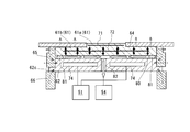
- FIG. 2 is an enlarged vertical sectional view of the substrate mounting table 15 of FIG. 2 is connected to an electrostatic chuck 61 made of aluminum nitride, a cooling jacket 62 made of aluminum disposed below the electrostatic chuck 61, and a lower side of the cooling jacket 62.
- a bracket 63 that forms a lift space for a wafer lifter driven by the lift cylinder 19 and a focus ring 64 disposed on the upper side of the electrostatic chuck 61 are configured.
- the electrostatic chuck 61 has an upper disk part 61a in which an electrode 71 for electrostatic adsorption is built, and a lower disk part having a larger diameter than the upper disk part 61a and in which a heater 72 is built in. 61b.
- the electrostatic chuck 61 is integrally formed of an upper disk part 61a and a lower disk part 61b.
- the substrate mounting table 15 in FIG. 2 includes an upper annular cover 65 for heat insulation that surrounds at least a part of the cooling jacket 62 and the lower disk portion 61b, and a lower side for heat insulation that surrounds the outer side of the bracket 63 in the radial direction.
- the cooling jacket 62 is sandwiched between the upper annular cover 65 and the lower annular cover 66.
- the electrode 71 for electrostatic attraction is connected to the power source 36 for electrostatic attraction, and the heater 72 for heating is connected to the power source 53 for heater of the temperature adjustment system 50.
- the upper disk portion 61a is formed in substantially the same planar shape and the same size as the substrate K placed on the upper surface.
- the heater 72 extends in a range of a diameter larger than the diameter of the substrate K in the lower disk portion 61b.
- the cooling jacket 62 includes an upper jacket main body 62a and a lower bottom 62b.
- the jacket main body 62 a is coupled to the lower surface of the electrostatic chuck 61 by a plurality of bolts 73.
- the bottom 62b is fitted into the lower recess of the jacket main body 62a, and is fixed to the jacket main body 62a by welding or the like.
- a coolant channel 74 for cooling is formed by the groove on the lower surface of the jacket main body 62a and the upper surface of the bottom 62b.
- the plurality of bolts 73 are arranged on one circumference centered on the mounting table axis O1.
- the refrigerant flow path 74 is formed in a spiral shape in a plan view, for example, and the refrigerant (Galden (registered trademark)) supplied from the chiller unit 51 flows through the connection port provided on the lower surface of the cooling jacket 62. By circulating through the path 74, the refrigerant that has taken away the heat of the wafer is returned to the chiller unit 51. In the chiller unit 51, the refrigerant is cooled and returned to the refrigerant flow path 74 again.
- heat removal means that the heat of the wafer is released outside through the surface of the bottom 62b of the cooling jacket 61.
- the heat of the wafer is released outside through the refrigerant, and a part of the heat of the wafer is radiated from the surface of the bottom 62b of the cooling jacket 61. This lowers the temperature of the wafer itself.
- the space surrounded by the bottom 62b of the cooling jacket 62 and the mounting table support member 69 is at atmospheric pressure.
- the refrigerant that has become hot due to the heat of the wafer is cooled in the chiller unit 51.
- An outward flange portion 62c is integrally formed at the lower end portion of the outer peripheral end in the radial direction of the jacket main body 62a.
- the flange portion 62c is composed of a ceramic upper annular cover 65 and a lower annular cover 66 for heat insulation. And are sandwiched from above and below.
- An annular notch 65a is formed at the upper end portion of the upper annular cover 65, and an inward flange portion 68a formed in the outer case 68 is engaged with the notch 65a.
- the upper end surface of the lower annular cover 66 abuts on the lower surface of the flange portion 62 c via the O-ring 75, and the lower end surface of the lower annular cover 66 abuts on the upper surface of the mounting table support member 69 via the O-ring 76.
- the upper annular cover 65 and the lower annular cover 66 are tightened from above and below by screwing bolts 77 inserted into the bolt insertion holes at the outer peripheral end of the outer case 68 into the female screw holes of the mounting table support member 69. .
- the focus ring 64 covers the upper surface of the lower disk part 61b outside the electrostatic disk 61 in the radial direction of the upper disk part 61a.
- the substrate K placed on the upper end chuck surface of the upper disk portion 61 a is located at substantially the same height as the upper surface of the focus ring 64.
- a minute gap 80 is formed between the upper surface of the jacket body 62a of the cooling jacket 62 and the lower surface of the electrostatic chuck 61 by increasing the surface roughness of the upper surface of the jacket body 62a.
- an O-ring 81 or an annular metal seal is disposed on the inner side of the circumference constituted by a plurality of bolts 73 for fixing the electrostatic chuck. It is configured in a sealed circular shape in plan view.
- a gas passage network 83 communicating with the central gas passage 82 of the shaft core O1 portion is formed on the upper surface of the jacket main body 62a.
- the central gas passage 82 communicates with a joint 85 screwed to the bracket 63 via a gas passage 84 formed in the bottom portion 62b.
- the joint 85 communicates with the vacuum pump 54 and the helium gas supply unit 52 of the temperature adjustment system 50 through a gas pipe 86 also serving as a suction pipe and a switching valve 87 so as to be switched.
- the helium gas supply unit 52 communicates with the upper surface (chuck surface) of the upper disk portion 61a through a joint 98 screwed to the bracket 63 and a gas passage, and can supply He gas to the back surface of the substrate K. It is configured as follows.
- FIG. 3 is a plan view of the cooling jacket 62 of FIG.
- a gas passage network 83 formed in a circular minute gap 80 surrounded by an O-ring 81 includes an outer annular passage 83a, an inner annular passage 83b, and both annular passages 83a and 83b.
- He gas supplied from the central gas passage 82 is evenly distributed over the entire circular minute gap 80. It is comprised so that it can supply to.
- the cooling jacket 62 is provided with a plurality of holes through which wiring for each power source is passed. Specifically, high-frequency power is applied to holes 90 and 96 through which wiring for electrostatic chuck power is passed, holes 93 and 94 through which wiring for heater power is passed, holes 89 and 97 for temperature monitor sensors, and electrodes on the mounting table. A hole 92 through which a wiring for applying a high frequency power is passed is provided. Further, lifter holes 88, 91, and 95 for lifting the back surface of the substrate K are provided.
- FIG. 4 is an explanatory view of the operation when the minute gap 80 is in a vacuum state at the time of temperature rise or standby
- FIG. 5 is when the minute gap 80 is in a He gas filling state during the process of placing the substrate K.
- FIGS. 4 and 5 are action explanatory views showing changes in the state in the minute gap 80, the solid line arrows show the heat transfer state, the white arrows show the He gas movement state, A broken arrow indicates a heat insulation state.
- the minute gap 80 is actually a thickness of several ⁇ m to several tens of ⁇ m, but is expressed in a greatly exaggerated state. As shown in FIG.
- the minute gap 80 is connected to the vacuum pump 54, and the He gas in the minute gap 80 is sucked to make the minute gap 80 in a vacuum state. Therefore, the minute gap 80 serves as a heat insulating layer, and it is possible to prevent the heat from the heater 72 from passing to the cooling jacket 62 side.
- the elevating cylinder 19 of FIG. 1 is lowered to place the substrate (wafer) K on the substrate mounting table 15 and attracted and held by the electrostatic chuck 61.
- the inside of the chamber 11 is heated to 120 ° C., for example, and the substrate K is heated to 200 ° C. by the heater 72 of the electrostatic chuck 61.
- SF 6 gas, SiF 4 gas, O 2 gas, inert gas, and the like supplied from the gas supply apparatus 20 into the upper chamber 12 by supplying high-frequency power to the coil 31 from the high-frequency power supply 32. Is turned into plasma.
- a high frequency voltage is also applied to the electrostatic chuck 61 from the high frequency power source 35.
- a potential difference is generated between the electrostatic chuck 61 and the plasma in the chamber 11, and ions in the plasma move toward the electrostatic chuck 61 due to the potential difference and collide with the surface of the substrate K. Etching is performed on the surface of the substrate K.
- SF 6 gas SiF 4 gas, O 2 gas, or the like is used in the plasma generation.
- a gas such as N 2 may be used depending on the object to be etched.
- the minute gap 80 is vacuumed because He gas is sucked by the vacuum pump 54. It is in a state.
- the minute gap 80 serves as a heat insulating layer, prevents heat from the heater 72 from passing to the cooling jacket 62 side, and prevents the heat from passing upward by the focus ring 64.
- the upper annular cover 65 prevents the heat from escaping outward. Thereby, the heat from the heater 72 can be collected in the central upper disk part 61. That is, the heat of the heater 62 can be efficiently collected in the upper disk portion 61. Therefore, efficient temperature rise can be achieved, power consumption of the heater 72 can be reduced, and energy saving can be achieved.
- the minute gap 80 is in a He gas filling state.
- the amount of heat generated by the substrate K is large, and it tends to be higher than a predetermined temperature of 200 ° C.
- the minute gap 80 is filled with He gas having a good heat transfer property, the heat of the substrate K can quickly pass through the minute gap 80 and reach (release) the cooling jacket 62. Therefore, the heat of the substrate K can be quickly removed to cool the substrate K. That is, it is possible to efficiently remove the heat from the substrate K.
- the back surface of the substrate K is filled with He gas having good heat transfer properties, the temperature distribution on the surface of the substrate K can be made uniform. Therefore, it is possible to suppress variations in the etching shape and etching rate due to variations in the temperature distribution on the surface of the substrate K.
- the electrostatic chuck 61 and the cooling jacket 62 shown in FIG. 2 are made of a ceramic focus ring 64 and a ceramic that have high heat insulating properties over the entire upper surface excluding the placement region of the substrate K and the entire outer region in the radial direction of the cooling jacket 62.
- the upper and lower annular covers 65 and 66 are covered. Examples of these ceramic materials include aluminum oxide (alumina), yttria, and quartz.
- the cooling action by the cooling jacket 62 can be concentrated on the electrostatic chuck 61, and the temperature rise of the substrate K can be suppressed. It becomes.
- the lower surface of the cooling jacket 62 is in an atmospheric pressure state, but is surrounded by the lower annular cover 66 and the mounting table support member 69, and therefore, the amount of heat released from the cooling jacket 62 by convection is very small.
- FIG. 6 is a graph showing temporal changes in the electrostatic chuck temperature, the heat removal amount, and the He gas pressure in the non-processed state.
- FIG. 6 shows a time lapse in a non-processing state from the heating step T1 of the electrostatic chuck 61 to the cooling step T3 by the cooling jacket 62 through the constant temperature step T2 in which the electrostatic chuck 61 is maintained at a temperature of 200 ° C.
- the change in the electrostatic chuck temperature (° C.) is indicated by a solid curve S1
- the change in the He gas pressure (Pa) in the minute gap 80 is indicated by a dashed curve S2
- the change in the heat removal amount (W) S3 is represented by two. This is indicated by a dashed line curve S3.
- the He gas pressure (Pa) in the minute gap 80 is reduced to about 100 Pa, which is close to absolute vacuum.
- the minute gap 80 functions as a heat insulating layer, and the heat removal to the cooling jacket 62 can be suppressed as much as possible as shown in FIG.
- the heating time for the temperature of the electrostatic chuck 61 to reach 200 ° C. from 50 ° C. in the heating step T1 was about 17 minutes.
- the amount of heat removal (W) could be reduced by reducing the He gas pressure (Pa).
- the heater 72 in FIG. 2 is stopped, and the minute gap 80 is in a state of being filled with He gas at approximately 1000 Pa as shown in FIG. Thereby, the heat removal amount (W) to the cooling jacket 62 increases to the maximum P1.
- FIG. 7 is a graph showing the temporal change of the electrostatic chuck temperature and the heater load factor in the non-processed state.
- FIG. 7 shows a time lapse in a non-process state following the cooling step T3 by the cooling jacket 62 through the constant temperature step T2 in which the electrostatic chuck 61 is maintained at a temperature of 200 ° C. from the heating step T1, as in FIG.
- the change of the electrostatic chuck temperature (° C.) and the load factor (%) of the heater 72 is shown.
- the change in the electrostatic chuck temperature is indicated by a solid curve S1
- the change in the load factor (%) of the heater 72 is indicated by a solid curve S4. It can be understood that when the current upper limit of the heater is 1 kW, the maximum load factor of the temperature raising step T1 is suppressed to about 40%, and the capacity of the heater 72 can be reduced.
- the heater 72 is arranged in a larger area than the substrate K, so that the temperature distribution on the electrostatic chuck 61 is uniform from the center of the substrate K to the outer peripheral edge. Distribution.
- the minute gap 80 that can be switched between the He gas filling state and the vacuum state is formed at the joint between the lower surface of the electrostatic chuck 61 and the upper surface of the cooling jacket 62, the non-processed state shown in FIG.
- the minute gap 80 is made into a vacuum state, thereby preventing the heat of the electrostatic chuck 61 from escaping to the cooling jacket 62 below, and efficient initial temperature rise and A standby state at a predetermined temperature can be maintained.
- the minute gap 80 is filled with the He gas, so that the heat of the high-temperature substrate K is quickly released to the cooling jacket 62 through the He gas having a good heat transfer property. It is possible to remove heat.
- the plasma processing apparatus 1 since the plasma processing apparatus 1 includes the substrate mounting table 15 that facilitates temperature control of the substrate K and the electrostatic chuck 61, temperature management during the processing of the substrate K can be easily performed. Can do. Therefore, it is possible to avoid non-uniform processing results where reproducibility due to unstable or non-uniform wafer temperatures cannot be obtained.
- the lower surface of the electrostatic chuck and the cooling jacket are directly joined, but the present invention is not limited to this.
- a heat insulating plate having a low thermal conductivity for example, a quartz plate
- a small gap may be formed between the upper surface and the upper surface. Even in this case, the same effect as the present embodiment can be obtained.
- the outer peripheral end portion in the radial direction of the minute gap 80 is sealed with an O-ring, but the present invention is not limited to this.
- the outer peripheral end portion of the minute gap 80 in the radial direction may be sealed with a heat-resistant metal seal. Even in this case, the same effect as the present embodiment can be obtained.
- the upper annular cover 65 and the lower annular cover 66 are formed as separate bodies, but they may be configured so as to be integrally formed. Even in this case, the same effect as the present embodiment can be obtained.
- the etching process has been described.
- the present invention is not limited to this, and the present invention can also be used for a film forming process using a CVD method (chemical vapor deposition method) or the like. Reaction heat may also be generated in this film forming process, and is particularly useful when precise temperature control is required at a temperature of about 100 to 300 ° C., which is a low temperature region of the film forming process.
- CVD method chemical vapor deposition method
- Plasma processing apparatus 15 Substrate mounting base 50 Temperature control system 52 Helium gas supply part 54 Vacuum pump 61 Electrostatic chuck 61a Upper disk part 61b Lower disk part 62 Cooling jacket 62c Flange part 64 Focus ring 65 Upper ring cover 66 Lower ring Cover 71 Electrode for electrostatic adsorption 72 Heater 74 Refrigerant flow path 80 Minute gap 81 O-ring
Landscapes
- Chemical & Material Sciences (AREA)
- Engineering & Computer Science (AREA)
- Physics & Mathematics (AREA)
- Plasma & Fusion (AREA)
- Analytical Chemistry (AREA)
- Mechanical Engineering (AREA)
- General Chemical & Material Sciences (AREA)
- Chemical Kinetics & Catalysis (AREA)
- Materials Engineering (AREA)
- Metallurgy (AREA)
- Organic Chemistry (AREA)
- Drying Of Semiconductors (AREA)
- Container, Conveyance, Adherence, Positioning, Of Wafer (AREA)
Abstract
L'invention concerne une plateforme de placement de substrat (15) qui permet d'améliorer l'effet de facteurs externes tels que la température dans une chambre (11). La plateforme de placement de substrat (15), qui est placée dans la chambre (11) dans un dispositif de traitement au plasma (1), comprend un mandrin électrostatique (61) et une chemise de refroidissement (62). Le mandrin électrostatique (61) comprend une partie de disque supérieure (61a) pourvue intérieurement d'une électrode d'attraction électrostatique (71), et une partie de disque inférieure (61b) plus grande en diamètre que la partie de disque supérieure (61a) et pourvue intérieurement d'un dispositif de chauffage (72). Une bague de focalisation (64) disposée radialement vers l'extérieur sur la partie de disque supérieure (61a) et recouvrant la surface supérieure de la partie de disque inférieure (61b), un couvercle annulaire supérieur (65) pour des fins d'isolation thermique qui renferme la partie de disque inférieure (61b) et au moins une partie de la chemise de refroidissement (62), et un couvercle annulaire inférieur (66) à des fins d'isolation thermique qui prend en sandwich la chemise de refroidissement (62) avec le couvercle annulaire supérieur (65) sont constitués d'un matériau céramique.
Priority Applications (4)
| Application Number | Priority Date | Filing Date | Title |
|---|---|---|---|
| EP19751281.7A EP3614423A4 (fr) | 2018-02-08 | 2019-01-09 | Plateforme de placement de substrat, dispositif de traitement au plasma la comprenant, et procédé de traitement au plasma |
| US16/613,975 US11393664B2 (en) | 2018-02-08 | 2019-01-09 | Substrate placing table, plasma processing apparatus provided with same, and plasma processing method |
| KR1020197024274A KR102627348B1 (ko) | 2018-02-08 | 2019-01-09 | 기판 재치대 및 이를 구비하는 플라즈마 처리 장치 및 플라즈마 처리 방법 |
| CN201980001478.7A CN110352482B (zh) | 2018-02-08 | 2019-01-09 | 基板载置台及其电浆处理装置以及电浆处理方法 |
Applications Claiming Priority (2)
| Application Number | Priority Date | Filing Date | Title |
|---|---|---|---|
| JP2018021302A JP6522180B1 (ja) | 2018-02-08 | 2018-02-08 | 基板載置台及びこれを備えたプラズマ処理装置及びプラズマ処理方法 |
| JP2018-021302 | 2018-02-08 |
Publications (1)
| Publication Number | Publication Date |
|---|---|
| WO2019155808A1 true WO2019155808A1 (fr) | 2019-08-15 |
Family
ID=66655701
Family Applications (1)
| Application Number | Title | Priority Date | Filing Date |
|---|---|---|---|
| PCT/JP2019/000283 Ceased WO2019155808A1 (fr) | 2018-02-08 | 2019-01-09 | Plateforme de placement de substrat, dispositif de traitement au plasma la comprenant, et procédé de traitement au plasma |
Country Status (7)
| Country | Link |
|---|---|
| US (1) | US11393664B2 (fr) |
| EP (1) | EP3614423A4 (fr) |
| JP (1) | JP6522180B1 (fr) |
| KR (1) | KR102627348B1 (fr) |
| CN (1) | CN110352482B (fr) |
| TW (1) | TWI812667B (fr) |
| WO (1) | WO2019155808A1 (fr) |
Families Citing this family (9)
| Publication number | Priority date | Publication date | Assignee | Title |
|---|---|---|---|---|
| US12288672B2 (en) * | 2020-01-15 | 2025-04-29 | Applied Materials, Inc. | Methods and apparatus for carbon compound film deposition |
| US11551916B2 (en) * | 2020-03-20 | 2023-01-10 | Applied Materials, Inc. | Sheath and temperature control of a process kit in a substrate processing chamber |
| US12606912B2 (en) | 2020-10-23 | 2026-04-21 | Applied Materials, Inc. | High heat loss heater and electrostatic chuck for semiconductor processing |
| KR102811688B1 (ko) | 2020-11-05 | 2025-05-26 | 주식회사 원익아이피에스 | 포커스 링 및 이를 포함하는 기판 처리 장치 |
| KR102608903B1 (ko) | 2021-04-12 | 2023-12-04 | 삼성전자주식회사 | 플라즈마 식각 장치 및 방법 |
| KR102823594B1 (ko) * | 2022-01-28 | 2025-06-23 | 주식회사 유진테크 | 기판 처리 장치 및 기판 처리 방법 |
| JP7583933B2 (ja) * | 2022-11-11 | 2024-11-14 | 日本碍子株式会社 | ウエハ載置台 |
| CN116892015A (zh) * | 2023-08-28 | 2023-10-17 | 北京北方华创微电子装备有限公司 | 承载装置和半导体工艺设备 |
| US20250183085A1 (en) * | 2023-11-30 | 2025-06-05 | Axcelis Technologies, Inc. | Large range heated electrostatic chuck |
Citations (6)
| Publication number | Priority date | Publication date | Assignee | Title |
|---|---|---|---|---|
| JP2001068538A (ja) | 1999-06-21 | 2001-03-16 | Tokyo Electron Ltd | 電極構造、載置台構造、プラズマ処理装置及び処理装置 |
| JP2006237348A (ja) | 2005-02-25 | 2006-09-07 | Ulvac Japan Ltd | 静電チャック及びこれを備えた真空処理装置 |
| JP2010123809A (ja) * | 2008-11-20 | 2010-06-03 | Tokyo Electron Ltd | 基板載置台および基板処理装置 |
| JP2013172013A (ja) * | 2012-02-21 | 2013-09-02 | Tokyo Electron Ltd | 基板処理装置、基板処理方法及び基板温度の設定可能帯域の変更方法 |
| JP2017174889A (ja) * | 2016-03-22 | 2017-09-28 | 東京エレクトロン株式会社 | 被加工物の処理装置 |
| US20170358475A1 (en) * | 2016-06-14 | 2017-12-14 | Samsung Electronics Co., Ltd. | Electrostatic chuck and plasma apparatus for processing substrates having the same |
Family Cites Families (21)
| Publication number | Priority date | Publication date | Assignee | Title |
|---|---|---|---|---|
| JP3263721B2 (ja) * | 1993-02-01 | 2002-03-11 | 東京エレクトロン株式会社 | 処理装置 |
| US5511799A (en) * | 1993-06-07 | 1996-04-30 | Applied Materials, Inc. | Sealing device useful in semiconductor processing apparatus for bridging materials having a thermal expansion differential |
| TW262566B (fr) * | 1993-07-02 | 1995-11-11 | Tokyo Electron Co Ltd | |
| KR20010068538A (ko) | 2000-01-06 | 2001-07-23 | 윤종용 | 반도체 장치의 테스트 패턴 형성 방법 |
| JP4312372B2 (ja) | 2000-12-11 | 2009-08-12 | 日本碍子株式会社 | 静電チャックおよびその製造方法 |
| JP3881908B2 (ja) * | 2002-02-26 | 2007-02-14 | 株式会社日立ハイテクノロジーズ | プラズマ処理装置 |
| EP1515363B1 (fr) | 2002-06-17 | 2011-03-23 | Mitsubishi Heavy Industries, Ltd. | Procede et dispositif de mesure du potentiel ou de la temperature d'une plaquette |
| JP5044931B2 (ja) | 2005-10-31 | 2012-10-10 | 東京エレクトロン株式会社 | ガス供給装置及び基板処理装置 |
| JP5069452B2 (ja) * | 2006-04-27 | 2012-11-07 | アプライド マテリアルズ インコーポレイテッド | 二重温度帯を有する静電チャックをもつ基板支持体 |
| US9275887B2 (en) * | 2006-07-20 | 2016-03-01 | Applied Materials, Inc. | Substrate processing with rapid temperature gradient control |
| JP5262878B2 (ja) * | 2009-03-17 | 2013-08-14 | 東京エレクトロン株式会社 | 載置台構造及びプラズマ成膜装置 |
| US9948214B2 (en) * | 2012-04-26 | 2018-04-17 | Applied Materials, Inc. | High temperature electrostatic chuck with real-time heat zone regulating capability |
| JP5989593B2 (ja) * | 2012-04-27 | 2016-09-07 | 日本碍子株式会社 | 半導体製造装置用部材 |
| JP5996340B2 (ja) * | 2012-09-07 | 2016-09-21 | 東京エレクトロン株式会社 | プラズマエッチング装置 |
| JP6080571B2 (ja) * | 2013-01-31 | 2017-02-15 | 東京エレクトロン株式会社 | 載置台及びプラズマ処理装置 |
| JP5811513B2 (ja) * | 2014-03-27 | 2015-11-11 | Toto株式会社 | 静電チャック |
| US9960060B2 (en) * | 2014-10-10 | 2018-05-01 | Varian Semiconductor Equipment Associates, Inc. | Platen assembly |
| JP6614933B2 (ja) | 2015-11-11 | 2019-12-04 | 東京エレクトロン株式会社 | 基板載置機構および基板処理装置 |
| US10612121B2 (en) * | 2016-03-14 | 2020-04-07 | Applied Materials, Inc. | Plasma resistant coating with tailorable coefficient of thermal expansion |
| CN108028135A (zh) | 2016-08-31 | 2018-05-11 | 科学与创新股份公司 | 超级电容器和制造方法 |
| JP6982394B2 (ja) * | 2017-02-02 | 2021-12-17 | 東京エレクトロン株式会社 | 被加工物の処理装置、及び載置台 |
-
2018
- 2018-02-08 JP JP2018021302A patent/JP6522180B1/ja active Active
-
2019
- 2019-01-09 EP EP19751281.7A patent/EP3614423A4/fr active Pending
- 2019-01-09 WO PCT/JP2019/000283 patent/WO2019155808A1/fr not_active Ceased
- 2019-01-09 CN CN201980001478.7A patent/CN110352482B/zh active Active
- 2019-01-09 US US16/613,975 patent/US11393664B2/en active Active
- 2019-01-09 KR KR1020197024274A patent/KR102627348B1/ko active Active
- 2019-01-16 TW TW108101690A patent/TWI812667B/zh active
Patent Citations (6)
| Publication number | Priority date | Publication date | Assignee | Title |
|---|---|---|---|---|
| JP2001068538A (ja) | 1999-06-21 | 2001-03-16 | Tokyo Electron Ltd | 電極構造、載置台構造、プラズマ処理装置及び処理装置 |
| JP2006237348A (ja) | 2005-02-25 | 2006-09-07 | Ulvac Japan Ltd | 静電チャック及びこれを備えた真空処理装置 |
| JP2010123809A (ja) * | 2008-11-20 | 2010-06-03 | Tokyo Electron Ltd | 基板載置台および基板処理装置 |
| JP2013172013A (ja) * | 2012-02-21 | 2013-09-02 | Tokyo Electron Ltd | 基板処理装置、基板処理方法及び基板温度の設定可能帯域の変更方法 |
| JP2017174889A (ja) * | 2016-03-22 | 2017-09-28 | 東京エレクトロン株式会社 | 被加工物の処理装置 |
| US20170358475A1 (en) * | 2016-06-14 | 2017-12-14 | Samsung Electronics Co., Ltd. | Electrostatic chuck and plasma apparatus for processing substrates having the same |
Also Published As
| Publication number | Publication date |
|---|---|
| TW201937591A (zh) | 2019-09-16 |
| US20210265141A1 (en) | 2021-08-26 |
| TWI812667B (zh) | 2023-08-21 |
| JP2019140211A (ja) | 2019-08-22 |
| JP6522180B1 (ja) | 2019-05-29 |
| KR20200117832A (ko) | 2020-10-14 |
| CN110352482A (zh) | 2019-10-18 |
| KR102627348B1 (ko) | 2024-01-19 |
| EP3614423A1 (fr) | 2020-02-26 |
| CN110352482B (zh) | 2024-06-07 |
| EP3614423A4 (fr) | 2020-12-30 |
| US11393664B2 (en) | 2022-07-19 |
Similar Documents
| Publication | Publication Date | Title |
|---|---|---|
| WO2019155808A1 (fr) | Plateforme de placement de substrat, dispositif de traitement au plasma la comprenant, et procédé de traitement au plasma | |
| US11289356B2 (en) | Stage and plasma processing apparatus | |
| TWI729871B (zh) | 用於高功率電漿蝕刻處理的氣體分配板組件 | |
| CN110120329B (zh) | 等离子体处理装置 | |
| TWI688668B (zh) | 具有可拆卸式氣體分配板之噴淋頭 | |
| JP5357639B2 (ja) | プラズマ処理装置およびプラズマ処理方法 | |
| JP7402255B2 (ja) | 高温用途のための着脱可能なバイアス可能な静電チャック | |
| US6549393B2 (en) | Semiconductor wafer processing apparatus and method | |
| JP5320171B2 (ja) | 基板処理装置 | |
| JP6469985B2 (ja) | プラズマ処理装置 | |
| JP2019519926A (ja) | 縁部シーリングを向上させた大電力用ワークピースキャリア | |
| JP2015220413A (ja) | 基板処理装置 | |
| JP2015076457A (ja) | 基板処理装置 | |
| US11984300B2 (en) | Plasma processing apparatus | |
| JP2017022295A (ja) | プラズマ処理装置 | |
| JP4355159B2 (ja) | 静電吸着ホルダー及び基板処理装置 | |
| JP5696183B2 (ja) | プラズマ処理装置 | |
| KR20110083979A (ko) | 플라즈마 처리 장치 | |
| JP4218822B2 (ja) | 真空断熱層を有する載置機構 | |
| US20040244949A1 (en) | Temperature controlled shield ring | |
| JP5953012B2 (ja) | 基板保持装置 | |
| KR102818096B1 (ko) | 기판 처리 장치 및 기판 처리 방법 |
Legal Events
| Date | Code | Title | Description |
|---|---|---|---|
| 121 | Ep: the epo has been informed by wipo that ep was designated in this application |
Ref document number: 19751281 Country of ref document: EP Kind code of ref document: A1 |
|
| ENP | Entry into the national phase |
Ref document number: 2019751281 Country of ref document: EP Effective date: 20191121 |
|
| NENP | Non-entry into the national phase |
Ref country code: DE |