WO2019182011A1 - Capteur de gaz et son procédé de fabrication - Google Patents
Capteur de gaz et son procédé de fabrication Download PDFInfo
- Publication number
- WO2019182011A1 WO2019182011A1 PCT/JP2019/011698 JP2019011698W WO2019182011A1 WO 2019182011 A1 WO2019182011 A1 WO 2019182011A1 JP 2019011698 W JP2019011698 W JP 2019011698W WO 2019182011 A1 WO2019182011 A1 WO 2019182011A1
- Authority
- WO
- WIPO (PCT)
- Prior art keywords
- electrode
- sensor element
- laminate
- green sheet
- gas sensor
- Prior art date
- Legal status (The legal status is an assumption and is not a legal conclusion. Google has not performed a legal analysis and makes no representation as to the accuracy of the status listed.)
- Ceased
Links
Images




Classifications
-
- G—PHYSICS
- G01—MEASURING; TESTING
- G01N—INVESTIGATING OR ANALYSING MATERIALS BY DETERMINING THEIR CHEMICAL OR PHYSICAL PROPERTIES
- G01N27/00—Investigating or analysing materials by the use of electric, electrochemical, or magnetic means
- G01N27/02—Investigating or analysing materials by the use of electric, electrochemical, or magnetic means by investigating impedance
- G01N27/04—Investigating or analysing materials by the use of electric, electrochemical, or magnetic means by investigating impedance by investigating resistance
- G01N27/12—Investigating or analysing materials by the use of electric, electrochemical, or magnetic means by investigating impedance by investigating resistance of a solid body in dependence upon absorption of a fluid; of a solid body in dependence upon reaction with a fluid, for detecting components in the fluid
-
- B—PERFORMING OPERATIONS; TRANSPORTING
- B28—WORKING CEMENT, CLAY, OR STONE
- B28B—SHAPING CLAY OR OTHER CERAMIC COMPOSITIONS; SHAPING SLAG; SHAPING MIXTURES CONTAINING CEMENTITIOUS MATERIAL, e.g. PLASTER
- B28B1/00—Producing shaped prefabricated articles from the material
- B28B1/30—Producing shaped prefabricated articles from the material by applying the material on to a core or other moulding surface to form a layer thereon
-
- B—PERFORMING OPERATIONS; TRANSPORTING
- B28—WORKING CEMENT, CLAY, OR STONE
- B28B—SHAPING CLAY OR OTHER CERAMIC COMPOSITIONS; SHAPING SLAG; SHAPING MIXTURES CONTAINING CEMENTITIOUS MATERIAL, e.g. PLASTER
- B28B1/00—Producing shaped prefabricated articles from the material
- B28B1/48—Producing shaped prefabricated articles from the material by removing material from solid section preforms for forming hollow articles, e.g. by punching or boring
-
- G—PHYSICS
- G01—MEASURING; TESTING
- G01N—INVESTIGATING OR ANALYSING MATERIALS BY DETERMINING THEIR CHEMICAL OR PHYSICAL PROPERTIES
- G01N27/00—Investigating or analysing materials by the use of electric, electrochemical, or magnetic means
- G01N27/02—Investigating or analysing materials by the use of electric, electrochemical, or magnetic means by investigating impedance
- G01N27/04—Investigating or analysing materials by the use of electric, electrochemical, or magnetic means by investigating impedance by investigating resistance
- G01N27/12—Investigating or analysing materials by the use of electric, electrochemical, or magnetic means by investigating impedance by investigating resistance of a solid body in dependence upon absorption of a fluid; of a solid body in dependence upon reaction with a fluid, for detecting components in the fluid
- G01N27/125—Composition of the body, e.g. the composition of its sensitive layer
-
- G—PHYSICS
- G01—MEASURING; TESTING
- G01N—INVESTIGATING OR ANALYSING MATERIALS BY DETERMINING THEIR CHEMICAL OR PHYSICAL PROPERTIES
- G01N27/00—Investigating or analysing materials by the use of electric, electrochemical, or magnetic means
- G01N27/26—Investigating or analysing materials by the use of electric, electrochemical, or magnetic means by investigating electrochemical variables; by using electrolysis or electrophoresis
- G01N27/403—Cells and electrode assemblies
- G01N27/406—Cells and probes with solid electrolytes
- G01N27/4067—Means for heating or controlling the temperature of the solid electrolyte
-
- G—PHYSICS
- G01—MEASURING; TESTING
- G01N—INVESTIGATING OR ANALYSING MATERIALS BY DETERMINING THEIR CHEMICAL OR PHYSICAL PROPERTIES
- G01N33/00—Investigating or analysing materials by specific methods not covered by groups G01N1/00 - G01N31/00
- G01N33/0004—Gaseous mixtures, e.g. polluted air
- G01N33/0009—General constructional details of gas analysers, e.g. portable test equipment
- G01N33/0027—General constructional details of gas analysers, e.g. portable test equipment concerning the detector
- G01N33/0036—General constructional details of gas analysers, e.g. portable test equipment concerning the detector specially adapted to detect a particular component
Definitions
- the present invention relates to a gas sensor for detecting a gas concentration in an atmosphere to be measured, for example, an oxygen concentration, and a manufacturing method thereof.
- Oxygen sensors made of various materials are known as detection elements for detecting the oxygen concentration.
- a material composition of an oxygen sensor using a ceramic sintered body an oxygen sensor using a composite ceramic in which LnBa 2 Cu 3 O 7- ⁇ and Ln 2 BaCuO 5 (Ln is a rare earth element) is known. (Patent Document 1).
- An oxygen sensor using a ceramic sintered body detects an oxygen concentration by using a hot spot phenomenon in which a part of a linear material (sensor element) becomes red hot when a voltage is applied.
- a hot spot type oxygen sensor has a characteristic that O 2 ⁇ ions taken into the crystal structure of the oxygen sensor element move to the positive electrode side.
- the hot spot generated at this time has a characteristic of moving to the negative electrode side where O 2 ⁇ ions are reduced.
- Patent Document 2 the constricted part provided in the sensor element made of a linear body or the like is used as the hot spot part, thereby the sensor element. A hot spot is generated at a specific position.
- Patent Document 3 the central portion of the element is constricted, and the cross-sectional area of the portion is reduced to increase the resistance value compared to other portions so that a hot spot appears in the constricted portion. ing.
- JP 2007-85816 Patent No. 4714867
- the conventional hot spot type oxygen sensor described above has an elongated rectangular parallelepiped shape with a uniform cross-sectional area, or an elongated rectangular parallelepiped shape having a constricted portion at the center of the element.
- a hot spot generating high heat is generated at a position close to the negative electrode, there is a problem that the electrode material is remarkably deteriorated.
- a hot spot is generated at a specific position of the element, or a constricted portion is provided in the element to ensure the appearance of the hot spot.
- a weak part will be formed and the intensity
- the provision of the constricted portion not only complicates the manufacturing process of the sensor element, but also causes deterioration of the oxygen sensor using the sensor element and a decrease in durability.
- the present invention has been made in view of the above-described problems, and an object of the present invention is to provide a gas sensor that can fix a hot spot generating portion without forming a fragile portion.
- the present invention is a gas sensor comprising a ceramic sintered body that detects a change in current value or resistance value when a voltage is applied to the sensor element as a gas concentration, and the sensor element is formed at both ends in the longitudinal direction.
- the cross-sectional area of the pair of electrode portions changes from one electrode side toward the other electrode side.
- the cross-sectional area increases or decreases uniformly or stepwise from the one electrode side toward the other electrode side.
- the sensor element has a constant thickness, and the width is increased or decreased uniformly or stepwise from the one electrode side toward the other electrode side.
- the sensor element is characterized in that the thickness and width increase or decrease uniformly or stepwise from the one electrode side toward the other electrode side.
- an electrode part formed on the side where the cross-sectional area of the sensor element is large among the pair of electrode parts is a negative electrode
- an electrode part formed on the side where the cross-sectional area is small is a positive electrode.
- the negative electrode and the positive electrode have substantially the same electrode size, or the electrode size of the negative electrode is larger than the electrode size of the positive electrode.
- both the minus electrode and the plus electrode are formed on the same surface side of the sensor element, or one of the minus electrode and the plus electrode is formed on the upper surface side of the sensor element, and the other is the It is formed on the lower surface side of the sensor element.
- a gas sensor manufacturing method is a gas sensor manufacturing method comprising a ceramic sintered body that detects a change in current value or resistance value as a gas concentration when a voltage is applied to a sensor element, the sensor comprising: A step of producing a green sheet from a slurry formed by mixing raw materials of the device, a step of producing a ring-shaped first green sheet formed by punching the green sheet to form punch holes of a predetermined diameter, and the first A step of producing a ring-shaped second green sheet in which strip-shaped electrodes are formed along the peripheral edge of the punch hole of the green sheet and the outer peripheral edge of the ring of the sheet; and A step of producing a ring-shaped laminate that is laminated in a coaxial state with a plurality of the first green sheets as the uppermost layer; and Cutting the laminate along a plurality of imaginary lines in the diameter direction of the ring-shaped laminate formed by rotating in the circumferential direction by a predetermined angle around the center, and sensor elements separated by the cutting And a step
- the cutter is disposed in the upper part of the laminate while rotating the laminate in the circumferential direction by a certain angle around the axis and synchronizing with the rotation. Cut the laminate by moving a predetermined distance downward, or fix the ring-like laminate, and place the cutter part arranged at the top of the laminate around the axis of the laminate at a certain angle. The laminate is cut by moving a predetermined distance downward in the vertical direction while rotating in the direction.
- a method for manufacturing a gas sensor according to the present invention is a method for manufacturing a gas sensor comprising a ceramic sintered body that detects a change in a current value or a resistance value when a voltage is applied to a sensor element as a gas concentration.
- the method includes a step of manufacturing a trapezoidal separated sensor element, and a step of firing the separated sensor element to form a pair of electrodes at both ends in the longitudinal direction.
- the present invention it is possible to fix the hot spot generation position in the gas sensor and prevent the electrode portion from being deteriorated by the hot spot.
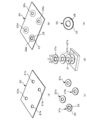
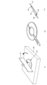
- FIG. 1 is an external perspective view of an oxygen sensor according to an embodiment of the present invention. It is a flowchart which shows the manufacturing process of the oxygen sensor which concerns on the example of this embodiment in time series. It is a figure which shows the mode of the process of the member etc. corresponding to each manufacturing process of FIG. It is a figure which shows the mode of the process of the member etc. corresponding to each manufacturing process of FIG. 10 is a diagram illustrating a manufacturing example of a sensor element according to Modification Example 1.
- FIG. 14 is an external perspective view of a sensor element according to Modification 2.
- FIG. It is a figure which shows the sensor element which concerns on the modification 3 in planar view. It is a figure which shows an example of the pattern which punches out the sensor element which concerns on the modification 3 from a green sheet.
- 14 is an external perspective view of a sensor element according to Modification 4.
- FIG. 1 is an external perspective view of an oxygen sensor according to an embodiment of the present invention.
- the oxygen sensor has a configuration in which a sensor element is accommodated inside a tubular body such as a cylindrical glass tube made of heat-resistant glass, but the tubular body is omitted here.
- An oxygen sensor 10 according to the present embodiment shown in FIG. 1 includes a sensor element 12, a pair of electrodes 13 and 15 formed opposite to both ends in the longitudinal direction of the sensor element 12, and electrodes 13 and 15, respectively. And lead wires 17 and 19 connected to each other.
- the sensor element 12 has a shape in which the element cross-sectional area on one electrode side and the element cross-sectional area on the other electrode side are different. Specifically, the cross-sectional area of the sensor element 12 increases uniformly from the plus (+) side electrode 13 toward the minus ( ⁇ ) side electrode 15.
- the ratio with the area S2 is, for example, 1.5: 1 to 2: 1.
- the sensor element 12 is made of a ceramic sintered body in which, for example, LnBa 2 Cu 3 O 7- ⁇ and Ln 2 BaCuO 5 are mixed.
- Ln is a rare earth element (for example, Sc (scandium), Y (yttrium), La (lanthanum), Nd (neodymium), Sm (samarium), Eu (europium), Gd (gadolinium), Dy (dysprosium). , Ho (holmium), Er (erbium), Tm (thulium), Yb (ytterbium), Lu (lutetium) and the like. Further, ⁇ represents an oxygen defect (0 to 1).
- an oxygen sensor is housed in a cylindrical glass tube made of heat-resistant glass with metal conductive caps (caps) made of copper (Cu) or the like attached to both ends. A current was passed through the sensor element connected to a power source, and the appearance of hot spots was observed.
- a hot spot is generated near the negative electrode of the sensor element.
- a hot spot is generated in the center of the sensor element. I understood.
- the hot spot generation position can be set to a position that is at an approximately equal distance from the pair of electrodes formed at both ends of the sensor element. Therefore, the damage to the electrode part by hot spot heat can be avoided. Further, since it is not necessary to provide a constricted portion in the sensor element as in the prior art in order to control the position where the hot spot is generated, it is possible to avoid the formation of a fragile portion in the sensor element.
- FIG. 2 is a flowchart showing the manufacturing process of the oxygen sensor according to the present embodiment in time series.
- a method for manufacturing the oxygen sensor shown in FIG. 3 and 4 show the processing of members corresponding to the respective manufacturing steps of the oxygen sensor shown in FIG.
- step S1 of FIG. 2 the raw materials of the sensor element of the oxygen sensor are mixed and pulverized. Specifically, LnBa 2 Cu 3 O 7- ⁇ and Ln 2 BaCuO 5 (Ln is a rare earth element) are mixed as materials of the oxygen sensor element, and the mixed raw material is pulverized with a ball mill or the like to prepare grains.
- step S2 the material obtained in the above process is subjected to heat treatment (calcination) at 900 to 1000 ° C., for example.
- step S3 the calcined raw material is pulverized by a ball mill or the like to prepare grains, and then a slurry is prepared.
- the calcined material includes a binder resin (for example, butyral resin (PVB resin), a dispersant (for example, sorbitan trioleate), a plasticizer (for example, bis (2-ethylhexyl phthalate), DOP), a diluent solvent (For example, 2-ethylhexanol) is mixed.
- step S4 a film is formed by a doctor blade to produce a green sheet of about 10 to 100 ⁇ m, for example.
- step S5 for example, as shown in FIG. 3A, center circles 21a to 21d are punched into the green sheet 20 by a mechanical punch or the like.
- Step S6 is a process in which a ring-shaped green sheet 27a positioned in the uppermost layer of a laminate to be described later and ring-shaped green sheets 27b to 27d stacked in the lower layer are formed on the same sheet, and electrodes are printed. Specifically, as shown in FIGS. 3A and 3B, along the inner peripheral edge of the center circle 21a corresponding to the center circle of the ring-shaped green sheet 27a as the uppermost layer of the laminate, for example, silver ( Ag) The positive electrode 25 is formed by screen printing an electrode material made of paste in a ring shape.
- the electrode material is formed in a ring shape along the outer peripheral portion 22a at a distance from the center of the center circle 21a to the radius of the ring-shaped green sheet 27a (that is, the length in the major axis direction of the sensor element). Is screen-printed to form the negative electrode 23.
- the other central circles 21b to 21d are left without being formed with electrodes.
- step S7 outer peripheral portions 22a to 22d defined according to the radius of the ring-shaped green sheet (the length of the sensor element) from the center of the central circles 21a to 21d (the outer peripheral portion 22a is the negative electrode 23 of the central circle 21a).
- the green sheet 20 is punched out by a mechanical punch or the like along the outer periphery.
- FIG. 3C shows green sheets (ring-shaped green sheets) 27a to 27d punched from the green sheet 20 and formed into a ring shape.
- step S8 as shown in FIG. 3D, a ring-shaped green sheet 27a in which electrode portions 23 and 25 are formed on the inner and outer peripheral portions at the uppermost portion of the ring-shaped green sheets 27b to 27d without electrodes.
- the rod-shaped pins 31 are inserted into the center holes of these ring-shaped green sheets and aligned.
- the laminated body of a ring-shaped green sheet is pressurized, for example with a uniaxial press, and the laminated body 33 of the predetermined thickness shown in FIG.3 (e) is produced.
- a ring-shaped green sheet 27a and three ring-shaped green sheets 27b to 27d are laminated to produce a laminated body.
- the number of laminated sheets is not limited to this, and the thickness of the produced laminated body is not limited to this.
- a required number of ring-shaped green sheets are stacked in accordance with the above.
- step S9 the laminate 33 is cut (diced) according to the size of the product (sensor element).
- the laminated body 33 is adsorbed and fixed to the guillotine stage 35, and the guillotine stage 35 is fixed at an angle (for example, 10 degrees) with the circle center of the laminated body 33 as an axis.
- the cutter 37 is moved vertically downward by a predetermined distance to cut the laminate 33.
- step S10 the sensor element 32 cut in the dicing process and separated into pieces as shown in FIG. 4B is baked in the atmosphere, for example, at 920 ° C. for 10 hours. Note that a binder may be removed from the laminate before firing, and the laminate after firing may be annealed.
- lead wires 47 and 49 are attached to the plus electrode 43 and the minus electrode 45 of the fired sensor element 42 by, for example, a conductive paste.
- the method for attaching the lead wire is not limited to the above.
- the joint may be instantaneously heated and soldered or welded using a pulse heat power source, or wire bonding by ultrasonic vibration or thermocompression bonding is used. May be.
- the sensor element singulated and fired as described above has a length of, for example, 5 mm, and the outer dimensions (size) of the oxygen sensor are, for example, a glass tube having a diameter of 5 mm, a length of 20 mm, and a vent hole.
- the diameter is 2.5 mm. Therefore, by setting the sensor element to the above dimensions, in the oxygen sensor, for example, the sensor element can be replaced through a vent hole of a glass tube.
- the pair of electrodes 13 and 15 are formed on both ends of the sensor element 12 on the same surface (upper surface) side in the longitudinal direction.
- a pair of electrodes may be formed on the upper surface side of one end of 12 and the lower surface side of the other end.
- both side surfaces in the axial direction of the oxygen sensor 10 in FIG. 1 extend in a straight line shape in plan view between the plus electrode and the minus electrode, but are not limited thereto. As long as the requirement that the cross-sectional area increases uniformly between both electrodes of the sensor element, even if both side surfaces between the plus electrode and minus electrode change to a planar curve, or one side has a curved curve. The shape which changes and the other side surface changes to planar view linear form may be sufficient.
- the present embodiment In the oxygen sensor according to the example, the cross-sectional area of the sensor element increases uniformly from the plus (+) electrode side toward the minus ( ⁇ ) electrode side, so that the oxygen sensor tries to move toward the minus electrode side.
- the hot spot can be guided to the low resistance side.
- the position where the hot spot is generated can be set to an approximately equal position from the pair of electrodes formed at both ends of the sensor element.
- the hot spot approaches the electrode part and the electrode is damaged by the hot spot heat. It is possible to prevent cracks from occurring in the sensor element or the like due to thermal stress due to expansion.
- the minus side electrode size can be made larger than the plus side.
- the oxygen sensor according to the present invention is not limited to the above embodiment, and various modifications are possible. Hereinafter, modified examples will be described.
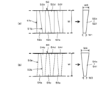
- FIGS. 5A and 5B show an example in which a sensor element is manufactured by dicing a belt-shaped green sheet.
- a long green sheet 50 having a width W that matches the dimension in the longitudinal direction of the sensor element (the length in the long axis direction) is prepared.
- the sheet 50 is cut along a cutting line in the width direction.
- the long green sheet 50 is diced along a cutting line 51a that runs in the width direction of the long green sheet 50 and a cutting line 51b that runs diagonally in the width direction.
- sensor elements 52a to 52f having a shape in which the width W1 on one end side is smaller than the width W2 on the other end side and the cross-sectional area uniformly increases from one end to the other end can be manufactured.
- FIG. 5B shows an example in which the long green sheet 50 is diced along two cutting lines 53 a and 53 b that run obliquely in the width direction of the long green sheet 50.
- sensor elements 54a to 54f having a shape in which the width W3 on one end side is smaller than the width W4 on the other end side and the cross-sectional area uniformly increases from the one end toward the other end can be manufactured.
- the sensor element is not limited to an example in which the overall shape is a flat plate like the sensor element shown in FIG. .
- a sensor element 62 shown in FIG. 6A has a one end bottom surface smaller in area than the other end bottom surface, and has a pyramidal shape as a whole.
- lead wires 63 and 65 are attached to electrodes (not shown) arranged on the bottom surface of one end and the bottom surface of the other end, respectively.
- the sensor element 64 shown in FIG. 6B has a one end bottom surface smaller than the other end bottom surface, and has a conical shape as a whole. Also in this example, lead wires 67 and 69 are attached to electrodes (not shown) arranged on one bottom surface and the other bottom surface, respectively.
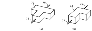
- FIG. 7A shows an example in which the sensor element 72 has a T-shape when viewed in plan.
- the cross-sectional area from the side where the lead wire 73 is attached to the side where the lead wire 75 is attached increases stepwise.
- FIG. 7B is an example in which the shape of the sensor element 74 when viewed in plan is an L-shape. In this example as well, the direction from the side where the lead wire 77 is attached to the side where the lead wire 79 is attached. The cross-sectional area increases stepwise.
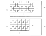
- FIG. 8A shows an example of a punching pattern in the case where a large number of T-shaped sensor elements 72 shown in FIG. 7A are punched from one green sheet 70.
- FIG. 8B shows an example of a punching pattern when a large number of L-shaped sensor elements 74 shown in FIG. 7B are punched from one green sheet 80.
- the number of sensor elements to be taken on one green sheet can be maximized.
- ⁇ Modification 4> In the third modification, the example in which the cross-sectional area of the flat sensor element is increased stepwise has been described.
- a sensor element having a three-dimensional shape in which the cross-sectional area increases stepwise will be described.
- the sensor element 82 in FIG. 9A has a shape formed by connecting two rectangular parallelepipeds having different cross-sectional areas. Further, lead wires 83 and 85 are attached to both end faces of the sensor element 82.
- the sensor element 84 in FIG. 9B has a shape in which two cylinders having different cross-sectional areas are connected. Also in the sensor element 84, lead wires 87 and 89 are attached to both end faces thereof. Therefore, in both the sensor element 82 in FIG. 9A and the sensor element 84 in FIG. 9B, the cross-sectional area of the sensor element gradually increases from one end to the other end.
Landscapes
- Chemical & Material Sciences (AREA)
- Health & Medical Sciences (AREA)
- Life Sciences & Earth Sciences (AREA)
- Engineering & Computer Science (AREA)
- Pathology (AREA)
- Physics & Mathematics (AREA)
- Analytical Chemistry (AREA)
- Biochemistry (AREA)
- General Health & Medical Sciences (AREA)
- General Physics & Mathematics (AREA)
- Immunology (AREA)
- Electrochemistry (AREA)
- Chemical Kinetics & Catalysis (AREA)
- Ceramic Engineering (AREA)
- Manufacturing & Machinery (AREA)
- Mechanical Engineering (AREA)
- Medicinal Chemistry (AREA)
- Food Science & Technology (AREA)
- Combustion & Propulsion (AREA)
- Molecular Biology (AREA)
- Measuring Oxygen Concentration In Cells (AREA)
- Investigating Or Analyzing Materials By The Use Of Fluid Adsorption Or Reactions (AREA)
Abstract
La présente invention a pour objet de fournir un capteur de gaz qui peut immobiliser l'emplacement d'occurrences de points chauds dans un élément de capteur. À cet effet, un élément de capteur (12) est formé de telle sorte que sa surface de section transversale augmente de manière uniforme ou pas à pas à partir du côté électrode positive (+) jusqu'au côté électrode négative (-) de sorte à induire les points chauds, qui, sinon, se déplaceraient vers le côté électrode négative, vers un côté à faible résistance. Par conséquent, des positions sensiblement égales à partir d'une paire d'électrodes (13, 15) formées au niveau des deux sections d'extrémité de l'élément de capteur (12) sont fixées de sorte à être des positions d'occurrence de points chauds, ce qui évite d'endommager des sections d'électrode en raison de la chaleur de point chaud.
Priority Applications (4)
| Application Number | Priority Date | Filing Date | Title |
|---|---|---|---|
| CN201980020754.4A CN111886494B (zh) | 2018-03-23 | 2019-03-20 | 气体传感器及其制造方法 |
| US17/040,278 US20210010963A1 (en) | 2018-03-23 | 2019-03-20 | Gas sensor and manufacturing method therefor |
| EP19770302.8A EP3770592B1 (fr) | 2018-03-23 | 2019-03-20 | Capteur de gaz et procédés de fabrication |
| US18/206,816 US12493010B2 (en) | 2018-03-23 | 2023-06-07 | Gas sensor |
Applications Claiming Priority (2)
| Application Number | Priority Date | Filing Date | Title |
|---|---|---|---|
| JP2018057303A JP7000222B2 (ja) | 2018-03-23 | 2018-03-23 | ガスセンサおよびその製造方法 |
| JP2018-057303 | 2018-03-23 |
Related Child Applications (2)
| Application Number | Title | Priority Date | Filing Date |
|---|---|---|---|
| US17/040,278 A-371-Of-International US20210010963A1 (en) | 2018-03-23 | 2019-03-20 | Gas sensor and manufacturing method therefor |
| US18/206,816 Division US12493010B2 (en) | 2018-03-23 | 2023-06-07 | Gas sensor |
Publications (1)
| Publication Number | Publication Date |
|---|---|
| WO2019182011A1 true WO2019182011A1 (fr) | 2019-09-26 |
Family
ID=67987323
Family Applications (1)
| Application Number | Title | Priority Date | Filing Date |
|---|---|---|---|
| PCT/JP2019/011698 Ceased WO2019182011A1 (fr) | 2018-03-23 | 2019-03-20 | Capteur de gaz et son procédé de fabrication |
Country Status (5)
| Country | Link |
|---|---|
| US (2) | US20210010963A1 (fr) |
| EP (1) | EP3770592B1 (fr) |
| JP (1) | JP7000222B2 (fr) |
| CN (1) | CN111886494B (fr) |
| WO (1) | WO2019182011A1 (fr) |
Families Citing this family (3)
| Publication number | Priority date | Publication date | Assignee | Title |
|---|---|---|---|---|
| CN111670360A (zh) * | 2018-01-31 | 2020-09-15 | 兴亚株式会社 | 氧传感器元件 |
| JP7643685B2 (ja) | 2021-06-17 | 2025-03-11 | 国立大学法人長岡技術科学大学 | 酸素センサ素子およびその製造方法 |
| JP7670270B2 (ja) | 2021-06-17 | 2025-04-30 | 国立大学法人長岡技術科学大学 | 抵抗型酸素ガスセンサ及び酸素センサ装置 |
Citations (6)
| Publication number | Priority date | Publication date | Assignee | Title |
|---|---|---|---|---|
| JPS52150696A (en) * | 1976-06-09 | 1977-12-14 | Nippon Soken | Detector for gas composition |
| JPH04115056U (ja) * | 1991-03-28 | 1992-10-12 | 横河電機株式会社 | セラミツクガスセンサ |
| JPH1073549A (ja) | 1996-08-30 | 1998-03-17 | Tokyo Gas Co Ltd | 自己発熱式酸素センサ |
| JP2000019143A (ja) | 1998-06-30 | 2000-01-21 | Toyota Motor Corp | 酸素濃度検出素子 |
| JP2000055857A (ja) * | 1998-08-03 | 2000-02-25 | Tokyo Gas Co Ltd | 酸素センサ素子 |
| JP2007085816A (ja) | 2005-09-21 | 2007-04-05 | Nagaoka Univ Of Technology | 酸素センサ |
Family Cites Families (12)
| Publication number | Priority date | Publication date | Assignee | Title |
|---|---|---|---|---|
| JP2000055855A (ja) * | 1998-08-04 | 2000-02-25 | Tokyo Gas Co Ltd | 自己発熱型ガスセンサ |
| US20030146093A1 (en) * | 2002-02-05 | 2003-08-07 | Kyocera Corporation | Oxygen sensor |
| JP3935754B2 (ja) * | 2002-03-27 | 2007-06-27 | 京セラ株式会社 | 酸素センサ素子 |
| JP2004226310A (ja) * | 2003-01-24 | 2004-08-12 | Kyocera Corp | 酸素センサ |
| US8603825B2 (en) * | 2004-03-31 | 2013-12-10 | Agency For Science, Technology And Research | Sensor for measuring gas permeability of a test material |
| US7278327B2 (en) * | 2004-07-26 | 2007-10-09 | New Jersey Institute Of Technology | Film based position and pressure sensor |
| JP2007273191A (ja) * | 2006-03-30 | 2007-10-18 | Toyota Motor Corp | 燃料電池 |
| US20110068091A1 (en) * | 2008-01-29 | 2011-03-24 | Kyocera Corporation | Ceramic Heater and Glow Plug |
| CN102954993B (zh) * | 2011-08-29 | 2015-07-22 | 比亚迪股份有限公司 | 一种氧传感器及其制备方法 |
| JP6643647B2 (ja) * | 2015-03-19 | 2020-02-12 | パナソニックIpマネジメント株式会社 | 感圧素子 |
| JP6523878B2 (ja) * | 2015-08-31 | 2019-06-05 | 日本特殊陶業株式会社 | ガスセンサ制御装置 |
| JP7000221B2 (ja) * | 2018-03-23 | 2022-01-19 | Koa株式会社 | ガスセンサおよびその製造方法 |
-
2018
- 2018-03-23 JP JP2018057303A patent/JP7000222B2/ja active Active
-
2019
- 2019-03-20 US US17/040,278 patent/US20210010963A1/en not_active Abandoned
- 2019-03-20 CN CN201980020754.4A patent/CN111886494B/zh active Active
- 2019-03-20 EP EP19770302.8A patent/EP3770592B1/fr active Active
- 2019-03-20 WO PCT/JP2019/011698 patent/WO2019182011A1/fr not_active Ceased
-
2023
- 2023-06-07 US US18/206,816 patent/US12493010B2/en active Active
Patent Citations (7)
| Publication number | Priority date | Publication date | Assignee | Title |
|---|---|---|---|---|
| JPS52150696A (en) * | 1976-06-09 | 1977-12-14 | Nippon Soken | Detector for gas composition |
| JPH04115056U (ja) * | 1991-03-28 | 1992-10-12 | 横河電機株式会社 | セラミツクガスセンサ |
| JPH1073549A (ja) | 1996-08-30 | 1998-03-17 | Tokyo Gas Co Ltd | 自己発熱式酸素センサ |
| JP2000019143A (ja) | 1998-06-30 | 2000-01-21 | Toyota Motor Corp | 酸素濃度検出素子 |
| JP2000055857A (ja) * | 1998-08-03 | 2000-02-25 | Tokyo Gas Co Ltd | 酸素センサ素子 |
| JP2007085816A (ja) | 2005-09-21 | 2007-04-05 | Nagaoka Univ Of Technology | 酸素センサ |
| JP4714867B2 (ja) | 2005-09-21 | 2011-06-29 | 国立大学法人長岡技術科学大学 | 酸素センサ |
Non-Patent Citations (1)
| Title |
|---|
| OKAMOTO, T. ET AL.: "Characteristics of Oxygen Sensor Exploiting the Hot Spot in BaAl2O4- added GdBa2Cu3O7-delta Composite Ceramic Rod", JOURNAL OF THE CERAMIC SOCIETY OF JAPAN, 2004, pages S567 - S571, XP055676622 * |
Also Published As
| Publication number | Publication date |
|---|---|
| JP7000222B2 (ja) | 2022-01-19 |
| US12493010B2 (en) | 2025-12-09 |
| US20210010963A1 (en) | 2021-01-14 |
| EP3770592A1 (fr) | 2021-01-27 |
| CN111886494A (zh) | 2020-11-03 |
| US20230349851A1 (en) | 2023-11-02 |
| EP3770592A4 (fr) | 2021-12-29 |
| JP2019168367A (ja) | 2019-10-03 |
| EP3770592B1 (fr) | 2023-09-27 |
| CN111886494B (zh) | 2024-06-04 |
Similar Documents
| Publication | Publication Date | Title |
|---|---|---|
| US12493010B2 (en) | Gas sensor | |
| KR102498100B1 (ko) | 적층 세라믹 콘덴서 | |
| US7598660B2 (en) | Monolithic piezoelectric element | |
| JP6314994B2 (ja) | 積層型セラミック電子部品 | |
| CN107437465B (zh) | 层叠陶瓷电容器 | |
| JP4854831B2 (ja) | 積層型圧電アクチュエータ | |
| CN107527736B (zh) | 多层陶瓷电容器 | |
| JP3797060B2 (ja) | セラミック積層体及びその製造方法 | |
| JP5655036B2 (ja) | 誘電体セラミックス、誘電体セラミックスの製造方法及び積層セラミックコンデンサ | |
| JP2005039068A (ja) | 積層セラミック電子部品の製造方法および積層セラミック電子部品 | |
| KR20180113163A (ko) | 적층 세라믹 콘덴서 및 그 제조 방법 | |
| JP7000221B2 (ja) | ガスセンサおよびその製造方法 | |
| JP2023120451A (ja) | 積層型コイル部品 | |
| CN112331444B (zh) | 线圈部件 | |
| CN218957480U (zh) | 层叠线圈部件 | |
| JP2009141143A (ja) | 積層型電子部品の製造方法 | |
| JP5409703B2 (ja) | 積層型圧電アクチュエータの製造方法 | |
| KR102078010B1 (ko) | 적층 세라믹 커패시터의 제조 방법 | |
| CN115206648A (zh) | 线圈部件 | |
| JP4992192B2 (ja) | 圧電磁器の製造方法及び圧電素子 | |
| JPS61174681A (ja) | 積層圧電体の製造方法 | |
| JP5303823B2 (ja) | 圧電素子 | |
| CN112334432A (zh) | 陶瓷构件及电子元件 | |
| JP4396190B2 (ja) | 積層バリスタの製造方法 | |
| JPH0547508A (ja) | 積層型半導体磁器及びその製造方法 |
Legal Events
| Date | Code | Title | Description |
|---|---|---|---|
| 121 | Ep: the epo has been informed by wipo that ep was designated in this application |
Ref document number: 19770302 Country of ref document: EP Kind code of ref document: A1 |
|
| NENP | Non-entry into the national phase |
Ref country code: DE |
|
| ENP | Entry into the national phase |
Ref document number: 2019770302 Country of ref document: EP Effective date: 20201023 |