WO2019231028A1 - Film isolant et procédé de fabrication d'un film isolant - Google Patents
Film isolant et procédé de fabrication d'un film isolant Download PDFInfo
- Publication number
- WO2019231028A1 WO2019231028A1 PCT/KR2018/006299 KR2018006299W WO2019231028A1 WO 2019231028 A1 WO2019231028 A1 WO 2019231028A1 KR 2018006299 W KR2018006299 W KR 2018006299W WO 2019231028 A1 WO2019231028 A1 WO 2019231028A1
- Authority
- WO
- WIPO (PCT)
- Prior art keywords
- resin
- film
- insulating
- thin film
- coating
- Prior art date
- Legal status (The legal status is an assumption and is not a legal conclusion. Google has not performed a legal analysis and makes no representation as to the accuracy of the status listed.)
- Ceased
Links
Images




Classifications
-
- B—PERFORMING OPERATIONS; TRANSPORTING
- B32—LAYERED PRODUCTS
- B32B—LAYERED PRODUCTS, i.e. PRODUCTS BUILT-UP OF STRATA OF FLAT OR NON-FLAT, e.g. CELLULAR OR HONEYCOMB, FORM
- B32B27/00—Layered products comprising a layer of synthetic resin
- B32B27/06—Layered products comprising a layer of synthetic resin as the main or only constituent of a layer, which is next to another layer of the same or of a different material
- B32B27/08—Layered products comprising a layer of synthetic resin as the main or only constituent of a layer, which is next to another layer of the same or of a different material of synthetic resin
-
- B—PERFORMING OPERATIONS; TRANSPORTING
- B32—LAYERED PRODUCTS
- B32B—LAYERED PRODUCTS, i.e. PRODUCTS BUILT-UP OF STRATA OF FLAT OR NON-FLAT, e.g. CELLULAR OR HONEYCOMB, FORM
- B32B7/00—Layered products characterised by the relation between layers; Layered products characterised by the relative orientation of features between layers, or by the relative values of a measurable parameter between layers, i.e. products comprising layers having different physical, chemical or physicochemical properties; Layered products characterised by the interconnection of layers
- B32B7/04—Interconnection of layers
- B32B7/06—Interconnection of layers permitting easy separation
-
- B—PERFORMING OPERATIONS; TRANSPORTING
- B32—LAYERED PRODUCTS
- B32B—LAYERED PRODUCTS, i.e. PRODUCTS BUILT-UP OF STRATA OF FLAT OR NON-FLAT, e.g. CELLULAR OR HONEYCOMB, FORM
- B32B7/00—Layered products characterised by the relation between layers; Layered products characterised by the relative orientation of features between layers, or by the relative values of a measurable parameter between layers, i.e. products comprising layers having different physical, chemical or physicochemical properties; Layered products characterised by the interconnection of layers
- B32B7/04—Interconnection of layers
- B32B7/12—Interconnection of layers using interposed adhesives or interposed materials with bonding properties
-
- H—ELECTRICITY
- H05—ELECTRIC TECHNIQUES NOT OTHERWISE PROVIDED FOR
- H05K—PRINTED CIRCUITS; CASINGS OR CONSTRUCTIONAL DETAILS OF ELECTRIC APPARATUS; MANUFACTURE OF ASSEMBLAGES OF ELECTRICAL COMPONENTS
- H05K3/00—Apparatus or processes for manufacturing printed circuits
- H05K3/22—Secondary treatment of printed circuits
- H05K3/28—Applying non-metallic protective coatings
Definitions
- the present invention relates to an insulating film and a method of manufacturing the same, to a thin film-coated insulating film having excellent step filling performance of a printed circuit and a low elastic modulus, and a method of manufacturing the same.
- the printed circuit board includes a rigid printed circuit board, a flexible printed circuit board (FPCB), a touch & display module, etc. according to its physical characteristics.
- FPCB flexible printed circuit board
- the reason for using a variety of printed circuits is that the effects of integration of high-functions are slimming down by connecting or stacking each function.
- a flexible printed circuit board or a flexible printed circuit cable is used to connect modules having individual functions and stacked printed circuit boards to each other.
- a polyimide film is used as an insulating layer and a coverlay coated with a thermosetting adhesive on one surface thereof is used.
- Existing PI film type coverlay has low step filling ability in the FPCB of high density microcircuit, resulting in dehydration during soldering and corrosion of the printed circuit due to plating solution and cleaning liquid penetrated into the terminal part. There is a problem in that the durability is lowered.
- a short circuit of a cable connected to an anisotropic conductive film (ACF) may occur due to the stress of the PI film.
- ACF anisotropic conductive film
- the punched PI film type coverlay is formed by heat press, and the flexible insulating paste is printed and cured to insulate, but the liquid flows when the flexible insulating paste is printed. , Thickness control, cracking of the insulation paste. There is a problem that the productivity is lowered by the above process.
- the object of the present invention is that the use of conventional films such as PI film, the step filling performance is low, causing the corrosion of the printed circuit due to the plating solution and the cleaning liquid penetrated into the terminal portion, while the stress of the PI film
- a film such as a PI film
- it does not use an insulation paste that causes problems such as liquids, liquid flow, thickness control, breakage of insulation paste, and problems of productivity loss. It is to provide an insulating film and a method of manufacturing the same.
- the step fillability of the printed circuit is excellent and the elastic modulus is low. It is to provide a thin film coating insulation film and a method of manufacturing the same.
- it is possible to shorten the manufacturing process of the printed circuit by manufacturing the folded part by the coverlay lamination single process without using the insulation paste, and the liquid flow at the time of heat curing and poor liquid at the insulation paste printing process by not using the insulation paste.
- an insulating film and a method for manufacturing the same which can prevent a defect due to a crack problem after curing.
- the present invention develops a printed circuit protection coverlay used in a compact, slip, and highly integrated electronic device as a thin film coating product to improve step filling and minimize stress due to elasticity to improve durability. It also aims to provide ease of assembly of modules.
- the present invention prevents reverse bending and warping in a specific layer in a printed circuit board that is laminated in a complex and excellent filling properties to reduce noise in high-speed signal transmission to reduce signal integrity and RFI ( It is intended to provide stabilization of Radio Frequency Interference.
- the present invention is a carrier film; An insulation layer formed on one surface of the carrier film; An adhesive layer formed on the insulating layer; And it provides a thin film-coated insulating film excellent in the step filling of the printed circuit comprising a protective film formed on the adhesive layer and a low modulus of elasticity and a method of manufacturing the same.
- the present invention also comprises the steps of (a) forming an insulating layer on the carrier film; (b) forming an adhesive layer on the insulating layer; And (c) laminating a protective film on the adhesive layer to provide a thin film-coated insulating film having excellent step filling ability and a low modulus of elasticity, and a method of manufacturing the same.
- a carrier film and an insulating resin is coated using the insulating layer (insulation layer) ) Is coated on one side of the carrier film with a thin film coated insulation film including an adhesive layer in a B-stage state and a resin solution having an insulating function and an adhesive function on one surface thereof.
- a thin film-coated insulating film having excellent step filling ability of a printed circuit and a low elastic modulus and a method of manufacturing the same are provided.
- a thin film-coated insulating film having excellent step filling performance and low elastic modulus of a printed circuit having a filling rate of 75% or more and an elastic modulus of 15 g ⁇ f / cm 2 or less, and a method of manufacturing the same.
- the thin film coating insulating film has excellent filling property in the step of the metal circuit, and thus, the plating liquid and the plating cleaning liquid do not penetrate into the circuit in the plating process of the micro circuit, so that the terminal part does not appear and the solder (Solder) does not appear. Delamination due to heat in the process can be prevented.
- the thin film-coated insulating film according to the present invention can be applied to a printed circuit board requiring low elasticity due to low stress characteristics.
- the process can be shortened by manufacturing a folded portion in a single step of covering the coverlay without using an insulation paste, and in an insulation paste printing process without using an insulation paste. It is possible to prevent the poor liquid due to the liquid problem, the liquid flow during heat curing, and the problem of cracks after curing.
- Figure 1 shows the structure of a thin film coating insulation film of the present invention.
- Figure 2 shows a manufacturing method (lamination production) of a thin film coating insulation film using a carrier film of the present invention.
- Figure 3 shows a method (manufacturing) of the thin film coating type insulating film using the carrier film of the present invention.
- FIG. 4 shows a flexible printed circuit board (FPCB) lamination method of the thin film coating insulation film of the present invention.
- FPCB flexible printed circuit board
- Figure 5 shows the environmental reliability observation results of Experimental Example 2.
- Figure 6 shows the chemical resistance evaluation results of Experimental Example 3.
- Figure 8 shows the step filling evaluation results of Experimental Example 6.
- Dispersion 2 was prepared by filtering the dispersed solution with SUS # 1000mesh.
- Dispersed solution 3 was prepared by filtering the dispersed solution with SUS # 1000mesh.
- Insulation composition 1 was applied to a carrier film (Thickness 23 ⁇ m, PET film) by a slot die coating method, dried at a temperature of 170 ° C. for 5 minutes to prepare an insulating layer having a thickness of 5 ⁇ m, and then oven temperature of 100 ° C. Aging was performed for 48 hours at.
- the adhesive composition was coated on the aged insulation layer coating film by a micro gravure coating method and dried at a temperature of 150 ° C. for 3 minutes to form a B-stage adhesive layer having a dry thickness of 5 ⁇ m. (PS 010 (50), A & S) It was laminated and aged in an oven at 40 ° C. for 72 hours to prepare Example 1.
- the insulating composition 1 was applied to a carrier film (Thickness 50 ⁇ m, PET film) by a slot die coating method, dried at a temperature of 170 ° C. for 5 minutes to prepare an insulating layer having a thickness of 10 ⁇ m, and then an oven temperature of 100 ° C. Aging was carried out for 72 hours at.
- the adhesive composition was coated on the aged insulation layer coating film by a micro gravure coating method and dried at a temperature of 150 ° C. for 3 minutes to form a B-stage adhesive layer having a dry thickness of 5 ⁇ m. (PS 010 (50), A & S) It was laminated and aged in an oven at 40 ° C. for 72 hours to prepare Example 2.
- the insulating composition 2 was applied to a carrier film (Thickness 50 ⁇ m, PET film) by a slot die coating method, dried at a temperature of 170 ° C. for 5 minutes to prepare an insulating layer having a thickness of 10 ⁇ m, and then an oven temperature of 100 ° C. Aging was performed for 48 hours at.
- the adhesive composition was coated on the aged insulation layer coating film by a micro gravure coating method and dried at a temperature of 150 ° C. for 3 minutes to form a B-stage adhesive layer having a dry thickness of 5 ⁇ m. (PS 010 (50), A & S) It was laminated and aged for 72 hours in a 40 °C oven to prepare Example 3.
- the insulating composition 2 was applied to a carrier film (Thickness 125 ⁇ m, PET film) by a slot die coating method, dried at a temperature of 170 ° C. for 5 minutes to prepare an insulating layer having a thickness of 10 ⁇ m, and then an oven temperature of 100 ° C. Aging was carried out for 72 hours at.
- the adhesive composition was applied to a release protective film (PS 010 (50), A & S) by a micro gravure coating method and dried at a temperature of 150 ° C. for 3 minutes to give a 5 ⁇ m B-stage. An adhesive layer was prepared.
- Example 4 was prepared by laminating with the carrier film coated with the insulating layer prepared above and aging in an oven at 40 ° C. for 72 hours.
- Example 5 After applying the insulating adhesive composition 1 to the carrier film (Thickness 50 ⁇ m, PET film) by the slot die coating method and drying for 2 minutes at a temperature of 140 °C by drying to form an insulating adhesive layer having a thickness of 20 ⁇ m release protective film (PS 010 (50), A & S) was laminated.
- the thin film-coated insulating adhesive film was aged in a 40 °C oven for 72 hours to prepare Example 5.
- Example 6 After applying the insulating adhesive composition 1 to the carrier film (Thickness 50 ⁇ m, PET film) by the slot die coating method and drying for 2 minutes at a temperature of 140 °C by drying to form an insulating adhesive layer having a thickness of 30 ⁇ m release protective film (PS 010 (50), A & S) was laminated.
- the thin film-coated insulating adhesive film was aged for 72 hours in a 40 °C oven to prepare Example 6.
- Heat-flexible epoxy-based insulation paste (NPR-5 / BR-HE No.1, Nippon Polytech Corp.) was printed on a test coupon (flexible printed circuit) using a 180mesh polyester plate, cured for 30 minutes in an oven at 150 °C. It was prepared by forming an insulating layer having a thickness of 10 ⁇ m on the printed circuit of the coupon.
- Heat-flexible epoxy-based insulation paste (NPR-5 / BR-HE No.1, Nippon Polytech Corp.) was printed on a test coupon (flexible printed circuit) using a 180mesh polyester plate, cured for 30 minutes in an oven at 150 °C. It was prepared by forming an insulating layer having a thickness of 20 ⁇ m on the printed circuit of the coupon.
- Heat-flexible epoxy-based insulation paste (NPR-5 / BR-HE No.1, Nippon Polytech Corp.) was printed on a test coupon (flexible printed circuit) using a 180mesh polyester plate, cured for 30 minutes in an oven at 150 °C. It was manufactured by forming an insulating layer having a thickness of 30 ⁇ m on the printed circuit of the coupon.
- Heat-resisting flexible polyester-based insulation paste (CR-18Y2-MS, Asahi Chemical) was printed on a test coupon (flexible printed circuit) using a 180mesh polyester plate and cured for 30 minutes in an oven at 150 ° C. It was prepared by forming an insulating layer of 20 ⁇ m.
- Heat-resisting flexible polyester-based insulation paste (CR-18Y2-MS, Asahi Chemical) was printed on a test coupon (flexible printed circuit) using a 180mesh polyester plate and cured for 30 minutes in an oven at 150 ° C. It prepared by forming the insulating layer of 30 micrometers.
- test coupon (flexible printed circuit) was placed on the circuit wiring part and was temporarily welded with a temporary connector (welding condition: 10 seconds, 150 ° C., 3 kg / cm 2 ), and then the carrier film was removed.
- the thin film-coated insulating film adjoined to the flexible printed circuit was completely cured by hot press (press condition: 60 minutes, 150 ° C., 30 kg / cm 2 ) to prepare a sample for evaluation.
- Tables 1 and 2 show the lamination structure, thickness, and sample fabrication cross-sectional structure for evaluation of Examples 1 to 6 and Comparative Examples 1 to 6.
- Example 1 Example 2
- Example 3 Example 4
- Example 5 Example 6 Carrier film thickness PET film23 ⁇ m PET film 50 ⁇ m PET film 50 ⁇ m PET film 125 ⁇ m PET film 50 ⁇ m PET film 125 ⁇ m Insulation layer thickness Insulation Composition 15 ⁇ m Insulation Composition 17.5 ⁇ m Insulation Composition 25 ⁇ m Insulation Composition 27.5 ⁇ m Insulation Adhesive Composition 120 ⁇ m Insulation Adhesive Composition 130 ⁇ m Adhesive layer thickness 5 ⁇ m 5 ⁇ m 5 ⁇ m 5 ⁇ m none none Manufacturing method Lamination Lamination Lamination Lamination Lamination Lamination Product form Coated Film Coated Film Coated Film Coated Film Coated Film Coated Film Coated Film Coated Film Evaluation sample
- FCCL Flexible Cooper Clad Laminate
- the prepared sample was evaluated according to the following evaluation method.
- Each of the evaluation samples shown in Tables 1 and 2 was floated on a 290 ° C. solder for 60 seconds to heat and left for 10 minutes at room temperature.
- the evaluation method was evaluated by visually observing the discoloration and bubble generation before and after the solder. If there is no change in the evaluation sample, Pass, and if there is a change, the changed evaluation item is indicated.
- a 98% purity isopropyl alcohol, 5% sulfuric acid (H 2 SO 4 ) aqueous solution, 5% sodium hydroxide (NaOH) aqueous solution was prepared.
- the prepared solution was placed in a 500 ml beaker, each 300 cc, into an ultrasonic cleaner (HSD-D250H, Korea Ultrasonic Co., Ltd.).
- the three solutions were warmed, and each of the evaluation samples shown in Tables 1 and 2 above was immersed in the solution at a temperature of 50 ° C. and ultrasonically cleaned for 30 minutes.
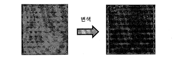
- the ultrasonically cleaned evaluation sample was washed with purified water and dried in a 50 ° C. oven for 30 minutes to visually evaluate the surface change (FIG. 6).
- FR4 rods used as steps were cut to a size of 5 mm in width and 25 cm in length.
- the cut FRP rods were arranged at intervals of 20 mm over Cu 1.0 Oz in thickness order and both ends were fixed with heat resistant tape.
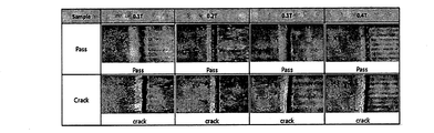
- the sample for evaluation was heated and pressurized with a heat press (60min. At 150 ° C, 30kg / cm 2) by placing an adhesive layer on the FRP rod in which the thin film-coated insulating films of Examples 1 to 6 and the coverlay of Comparative Example 6 were arranged. After fabrication, the FR4 edge was observed under a microscope to evaluate the presence of cracks (FIG. 7).
- the surface resistance measuring instrument (SRM-110, Wolfgang Warmbier) was placed on the insulating layer surface of each of the evaluation samples shown in Tables 1 and 2, and 5 points were measured to indicate the average of the displayed resistance values.
- Example and Comparative Example Evaluation Results Example 1 Example 2 Example 3 Example 4 Example 5 Example 6 Comparative Example 1 Comparative Example 2 Comparative Example 3 Comparative Example 4 Comparative Example 5 Comparative Example 6 Solder heat resistance Pass Pass Pass Pass Pass Pass Pass Pass Pass Pass Pass H 2 SO 4 Pass Pass Pass Pass Pass Pass Pass Oxidation Oxidation Pass Oxidation Oxidation Pass NaOH Pass Pass Pass Pass Pass Uplifting Uplifting Uplifting Uplifting Uplifting Uplifting Uplifting Uplifting Uplifting Uplifting Uplifting Uplifting Uplifting Uplifting Uplifting Uplifting Uplifting Uplifting Uplifting Uplifting Uplifting Uplifting Uplifting Uplifting Uplifting Uplifting Uplifting Uplifting Uplifting Uplifting Uplifting Uplifting Uplifting Uplifting Uplifting Uplifting Uplifting Uplifting Uplifting Uplifting Uplifting Uplifting Uplifting Uplifting Uplifting Uplifting Uplifting Uplifting Uplifting Uplifting Uplifting Uplifting Uplifting Up
- the present invention will be described in detail a thin film coating insulating film and a method of manufacturing a low-stress filled metal step of the printed circuit.
- Existing coverlay film is generally used for the purpose of protecting the wiring part and is manufactured by laminating a film (insulating layer) and an adhesive layer using synthetic resin such as polyimide resin.
- a film type coverlay is used by laminating an adhesive layer of a coverlay on a wiring portion of a printed circuit board (PCB) and laminating using a hot press.
- the coverlay used in the related art uses a film base material as an insulating layer, so the space filling rate between printed circuit wirings is low. It is a problem that the plating solution or the cleaning liquid penetrates into the gap and the circuit pattern is corroded or the solder is lifted due to the gap filling due to the thickness of the wiring. In addition, it is difficult to manufacture a film of a thin film and the use of a limited material has a high price. In addition, existing coverlays using PI film have high elasticity and require additional processing using insulating pastes, resulting in process defects.
- the carrier film used in the present invention is used as a base material for coating the insulating resin solution and used for curing and drying the insulating resin layer of the thin film.
- the thin film-coated insulating film may serve as a guide when the thin film-coated insulating film is attached to protect the wiring of the printed circuit so that the thin film-coated insulating film may be stacked at a predetermined position without wrinkles.
- the present invention in one aspect, a carrier film; An insulation layer formed on one surface of the carrier film; An adhesive layer formed on the insulating layer; And it relates to a thin film coating type insulating film comprising a protective film formed on the adhesive layer (Fig. 1).
- the thin film coating insulation film may use a carrier film as a coverlay.
- the present invention also comprises the steps of (a) forming an insulating layer on the carrier film; (b) forming an adhesive layer on the insulating layer; And (c) laminating a protective film on the adhesive layer, and a method of manufacturing a thin film-coated insulating film having excellent filling properties and low elastic modulus.
- the thin film coating insulation film may use a carrier film as a coverlay.
- the insulating film is manufactured by using a carrier film coated with an insulating layer directly on its surface, that is, the insulating film is manufactured without using films such as PI films, and thus the filling rate is 75% or more.
- the key technical characteristics are that the filling property is excellent, and the stress is low, the elastic modulus is 15 g.f / cm 2 or less.
- the plating solution and flushing liquid penetrate into the edge part of the circuit part in the plating process and vaporize and expand in the Surface Mount Technolongy (SMT) process. Even without lifting, the penetrated liquid causes oxidation of the metal circuit, causing problems in the durability of the product.
- SMT Surface Mount Technolongy
- the above problems in the PCB manufacturing process are caused by various factors such as the shape and circuit thickness of the metal circuit, the circuit line width, and the circuit space. Therefore, the above-mentioned problem is a fundamental solution.
- the fill rate of the metal circuit space of the coverlay using the PI film is less than 60%, and through the present invention, when the space filling rate is 75% or more, it was confirmed that the above-mentioned lifting or immersion in the plating process did not appear.
- a display panel or a touch panel is connected to the FPCB with an anisotropic conductive film (ACF).
- ACF anisotropic conductive film
- the adhesion area of ACF is reduced, resulting in relatively low adhesion, and the process conditions are also manufactured at low temperature and low pressure.
- an insulating paste having a low modulus of elasticity is printed on a bent portion by a screen printer to lower the elasticity to compensate for the attachment reliability of the ACF.
- Insulation pastes currently used are typically used with a dry thickness of 25 to 30 ⁇ m and have an elastic modulus of 16 g ⁇ f / cm 2 to 18 g.f / cm 2 when the thickness of the insulation paste is 30 ⁇ m.
- the insulating film is characterized in that it has an elastic modulus of 15g.f / cm2.
- Insulation film with low elastic modulus can be manufactured by reducing the process cost and improving production yield because it can manufacture flexible printed circuit with low elastic modulus in a single process by replacing the coverlay of the PI film and then applying the insulation paste. The cost can be reduced and the durability of the product can be improved.
- the insulating layer may be formed by a coating method using the carrier film.
- the adhesive layer may be prepared by directly laminating an adhesive resin on the insulating layer or by forming an adhesive layer on another film having releasability and laminating it with the insulating layer (FIGS. 2 and 3). .
- the carrier film is a PET film, semi-matt PET film, matt PET film, PEN film, PES film, TPU film, Nylon film, PVC film, synthetic paper and synthetic
- the resin may be characterized in that at least one selected from the group consisting of coated paper (resin coated paper), but is not limited thereto.
- coated paper resin coated paper
- low cost and various types of PET film may be used.
- release coated and untreated surfaces of the carrier film is selected according to the removal property of the carrier film after temporary welding or hot pressing.
- the heat deformation rate of the carrier film 60 minutes, 150 °C, 30 kg / cm 2 ) should be less than 1%.
- the thickness of the carrier film is preferably 20 to 125 ⁇ m.
- the thickness is less than 20 ⁇ m the thin film coating insulation film is laminated on the printed circuit it is difficult to be laminated in accordance with the punching position by bending or folding, there is a problem of wrinkles caused by the thin film.
- the thickness exceeds 125 ⁇ m there is a problem in the step filling of the metal circuit after the hot press, and there is a problem of poor edge burrs in the punching process of the thin film coating insulation film.
- the carrier film is removed after the temporary welding or hot pressing to be applied as a coverlay of a printed circuit board (PCB) (FIG. 4).
- PCB printed circuit board
- the present invention can be used in a variety of polymer insulating materials without using an expensive polyimide (Polyimide) film by using a carrier film there is an advantage in productivity and cost.
- Polyimide Polyimide
- the thickness of the insulating layer is preferably 2 to 12 ⁇ m. If the thickness is less than 2 ⁇ m, tearing occurs after the hot press at the printed circuit metal wiring step, and if the thickness is more than 12 ⁇ m, there is a problem that the step filling performance of the metal wiring portion is lowered. The amount of insulation resin solution applied increases the price.
- the insulating layer may be made of one or more selected from the group consisting of a thermoset resin, a thermoplastic resin, and a photocurable resin.
- the insulating layer may be an epoxy resin, a polyurethane resin, a polyester resin, a polyimide resin, an amide resin, or a phenoxy resin.
- resins may be characterized by consisting of at least one selected from the group consisting of ethylene acrylate resin (ethylene acrylate resin), urethane acrylate resin (urethane acrylate resin), epoxy acrylate resin (epoxy acrylate resin) and modified resin thereof, It is not limited to this.
- a flame retardant in the present invention, a flame retardant, a surfactant, an adhesion promoter and the like can be used for the insulating layer resin.
- Flame retardants include phosphorus flame retardants such as Triethyl phosphate (TEP), Resorcinol bis (diphenyl phosphate), RDP (Tricresyl phosphate), IPPP (Isopropylphenyl phosphate), or MCA (Melamine cyanurate), ATO (Aluminium trioxide) and ATH (Aluminium) inorganic flame retardants such as trihydrate, etc.
- the flame retardant is 15% compared to the resin to secure flame retardancy, and a silicone-based surfactant for preventing pin holes and leveling characteristics of the coating film when coating the carrier film.
- a silane coupling agent or a triazine derivative may be used.
- the adhesive layer may be characterized in that the semi-cured (B-stage) state.
- the adhesive layer should remain semi-cured after the coating is dried and should be completely cured by heat press after lamination with a printed circuit.
- the adhesive layer may be made of the same or different resin as the insulating layer resin.
- the adhesive layer may include an adhesion promoter and a surfactant to improve the function of the adhesive layer.
- the thickness after coating drying of the adhesive layer may be characterized in that preferably 3 to 30 ⁇ m.
- the thickness is less than 3 ⁇ m after drying, there is a problem that the resin flow (resin flow) in the heat press process is low, the step filling of the circuit wiring is low, and the adhesion to the printed circuit portion is lowered.
- the adhesive layer has a dry thickness of more than 30 ⁇ m, there is a problem that contamination and unplating of the plating terminal part occur due to excessive resin flow in the heat press process.
- the insulating layer and the adhesive layer may be formed by a single coating using a carrier film.
- a carrier film and an insulating resin is coated using the insulating layer (insulation layer) ) Is coated on one side of the carrier film with a thin film coated insulation film including an adhesive layer in a B-stage state and a resin solution having an insulating function and an adhesive function on one surface thereof.
- a thin film-coated insulating film having excellent step filling ability of a printed circuit and a low elastic modulus and a method of manufacturing the same are provided.
- a thin film-coated insulating film having excellent step filling performance and low elastic modulus of a printed circuit having a filling rate of 75% or more and an elastic modulus of 15 g ⁇ f / cm 2 or less, and a method of manufacturing the same.
- the thin film coating insulating film has excellent filling property in the step of the metal circuit, and thus, the plating liquid and the plating cleaning liquid do not penetrate into the circuit in the plating process of the micro circuit, so that the terminal part does not appear and the solder (Solder) does not appear. Delamination due to heat in the process can be prevented.
- the thin film-coated insulating film according to the present invention can be applied to a printed circuit board requiring low elasticity due to low stress characteristics.
- the process can be shortened by manufacturing a folded portion in a single step of covering the coverlay without using an insulation paste, and in an insulation paste printing process without using an insulation paste. It is possible to prevent the poor liquid due to the liquid problem, the liquid flow during heat curing, and the problem of cracks after curing.
Landscapes
- Engineering & Computer Science (AREA)
- Manufacturing & Machinery (AREA)
- Microelectronics & Electronic Packaging (AREA)
- Non-Metallic Protective Coatings For Printed Circuits (AREA)
- Laminated Bodies (AREA)
Abstract
La présente invention concerne un film isolant revêtu de film mince, comprenant un film de support, une couche isolante formée par revêtement d'une résine isolante à l'aide du film de support et une couche adhésive de stade B qui est agencée sur une surface de la couche isolante, ainsi qu'un film isolant revêtu de film mince comportant une solution de résine qui comporte des fonctions isolante et adhésive, revêtue sur une surface du film de support, de telle sorte que le rapport de remplissage d'une partie de câblage de circuit imprimé est d'au moins 75 % et que le module d'élasticité est d'au plus 15 g.f/cm2.
Priority Applications (1)
| Application Number | Priority Date | Filing Date | Title |
|---|---|---|---|
| PCT/KR2018/006299 WO2019231028A1 (fr) | 2018-06-01 | 2018-06-01 | Film isolant et procédé de fabrication d'un film isolant |
Applications Claiming Priority (1)
| Application Number | Priority Date | Filing Date | Title |
|---|---|---|---|
| PCT/KR2018/006299 WO2019231028A1 (fr) | 2018-06-01 | 2018-06-01 | Film isolant et procédé de fabrication d'un film isolant |
Publications (1)
| Publication Number | Publication Date |
|---|---|
| WO2019231028A1 true WO2019231028A1 (fr) | 2019-12-05 |
Family
ID=68698316
Family Applications (1)
| Application Number | Title | Priority Date | Filing Date |
|---|---|---|---|
| PCT/KR2018/006299 Ceased WO2019231028A1 (fr) | 2018-06-01 | 2018-06-01 | Film isolant et procédé de fabrication d'un film isolant |
Country Status (1)
| Country | Link |
|---|---|
| WO (1) | WO2019231028A1 (fr) |
Cited By (2)
| Publication number | Priority date | Publication date | Assignee | Title |
|---|---|---|---|---|
| CN113322714A (zh) * | 2020-02-28 | 2021-08-31 | 中国科学院成都有机化学有限公司 | 一种聚酰亚胺复配型抗高温老化助剂及其绝缘纸和制备方法 |
| CN114245582A (zh) * | 2021-12-16 | 2022-03-25 | 深圳市昶东鑫线路板有限公司 | 一种柔性电路板加工智造设备 |
Citations (5)
| Publication number | Priority date | Publication date | Assignee | Title |
|---|---|---|---|---|
| JP2001074933A (ja) * | 1999-09-01 | 2001-03-23 | Nitto Denko Corp | 表面保護フィルム |
| US20120320542A1 (en) * | 2011-06-16 | 2012-12-20 | Chang-Yong Jeong | Display device and method for manufacturing the same |
| KR20130096025A (ko) * | 2012-02-21 | 2013-08-29 | 삼성전기주식회사 | 플라잉테일 형태의 경연성 인쇄회로기판 제조 방법 및 이에 따라 제조된 플라잉테일 형태의 경연성 인쇄회로기판 |
| KR20140074700A (ko) * | 2012-12-10 | 2014-06-18 | 남광현 | 기능성 필름 및 이를 포함하는 연성회로기판 |
| KR20160103502A (ko) * | 2015-01-20 | 2016-09-01 | (주)창성 | 전자파 차폐시트 및 그 제조방법 |
-
2018
- 2018-06-01 WO PCT/KR2018/006299 patent/WO2019231028A1/fr not_active Ceased
Patent Citations (5)
| Publication number | Priority date | Publication date | Assignee | Title |
|---|---|---|---|---|
| JP2001074933A (ja) * | 1999-09-01 | 2001-03-23 | Nitto Denko Corp | 表面保護フィルム |
| US20120320542A1 (en) * | 2011-06-16 | 2012-12-20 | Chang-Yong Jeong | Display device and method for manufacturing the same |
| KR20130096025A (ko) * | 2012-02-21 | 2013-08-29 | 삼성전기주식회사 | 플라잉테일 형태의 경연성 인쇄회로기판 제조 방법 및 이에 따라 제조된 플라잉테일 형태의 경연성 인쇄회로기판 |
| KR20140074700A (ko) * | 2012-12-10 | 2014-06-18 | 남광현 | 기능성 필름 및 이를 포함하는 연성회로기판 |
| KR20160103502A (ko) * | 2015-01-20 | 2016-09-01 | (주)창성 | 전자파 차폐시트 및 그 제조방법 |
Cited By (3)
| Publication number | Priority date | Publication date | Assignee | Title |
|---|---|---|---|---|
| CN113322714A (zh) * | 2020-02-28 | 2021-08-31 | 中国科学院成都有机化学有限公司 | 一种聚酰亚胺复配型抗高温老化助剂及其绝缘纸和制备方法 |
| CN113322714B (zh) * | 2020-02-28 | 2022-12-02 | 中国科学院成都有机化学有限公司 | 一种聚酰亚胺复配型抗高温老化助剂及其绝缘纸和制备方法 |
| CN114245582A (zh) * | 2021-12-16 | 2022-03-25 | 深圳市昶东鑫线路板有限公司 | 一种柔性电路板加工智造设备 |
Similar Documents
| Publication | Publication Date | Title |
|---|---|---|
| US7293353B2 (en) | Method of fabricating rigid flexible printed circuit board | |
| WO2011162453A1 (fr) | Procédé de fabrication d'un film de blindage électromagnétique et film de blindage fabriqué à l'aide de ce procédé | |
| KR101361533B1 (ko) | 전자기파 차폐 필름 제조방법 | |
| WO2019124624A1 (fr) | Film de protection contre les ondes électromagnétiques, procédé de fabrication de carte de circuit imprimé, et procédé de fabrication de film de protection contre les ondes électromagnétiques | |
| WO2016105131A1 (fr) | Procédé de fabrication d'un film de blindage contre les ondes électromagnétiques pour carte de circuits imprimés souple | |
| WO2018101503A1 (fr) | Procédé de fabrication de carte de circuit imprimé et carte de circuit imprimé ainsi fabriquée | |
| WO2018151578A1 (fr) | Procédé de fabrication d'un film de transfert comprenant une couche de germe, procédé de fabrication de carte de circuit imprimé par gravure sélective de couche de germe, et composite de solution de gravure | |
| WO2012087072A2 (fr) | Carte de circuit imprimé et son procédé de fabrication | |
| WO2019231028A1 (fr) | Film isolant et procédé de fabrication d'un film isolant | |
| WO2013085229A1 (fr) | Carte à circuit imprimé et son procédé de fabrication | |
| WO2012053826A1 (fr) | Stratifié revêtu de métal de polyimide à couches épaisses | |
| WO2015105340A1 (fr) | Film de blindage contre les ondes électromagnétiques pour carte de circuit imprimé souple et son procédé de fabrication | |
| WO2018117636A1 (fr) | Stratifié métallique et procédé de fabrication de celui-ci | |
| WO2011010889A2 (fr) | Carte de circuit imprimé souple et son procédé de fabrication | |
| WO2014092386A1 (fr) | Carte de circuit imprimé et procédé de fabrication de celle-ci | |
| WO2019124930A1 (fr) | Plaque stratifiée métallique ductile destinée à un capteur tactile | |
| KR102240918B1 (ko) | 절연필름 및 절연필름의 제조방법 | |
| WO2013141611A1 (fr) | Carte de mémoire à semi-conducteurs, carte à circuits imprimés pour carte de mémoire et procédé de fabrication associé | |
| WO2016117720A1 (fr) | Feuille de protection contre les ondes électromagnétiques et son procédé de fabrication | |
| WO2018186654A1 (fr) | Carte de circuits imprimés et procédé de production associé | |
| WO2015056880A1 (fr) | Procédé de fabrication d'une carte de circuit imprimé | |
| JPH05160556A (ja) | プリント配線板 | |
| WO2016117719A1 (fr) | Film de protection contre les ondes électromagnétiques et son procédé de fabrication | |
| WO2018194367A1 (fr) | Procédé de fabrication de carte de circuit imprimé | |
| US20200288569A1 (en) | Circuit Board with Improved Thermal, Moisture Resistance, and Electrical Properties |
Legal Events
| Date | Code | Title | Description |
|---|---|---|---|
| 121 | Ep: the epo has been informed by wipo that ep was designated in this application |
Ref document number: 18920324 Country of ref document: EP Kind code of ref document: A1 |
|
| NENP | Non-entry into the national phase |
Ref country code: DE |
|
| 122 | Ep: pct application non-entry in european phase |
Ref document number: 18920324 Country of ref document: EP Kind code of ref document: A1 |