WO2019235189A1 - バスバー積層体及びそれを備える電子部品実装モジュール、バスバー積層体の製造方法 - Google Patents
バスバー積層体及びそれを備える電子部品実装モジュール、バスバー積層体の製造方法 Download PDFInfo
- Publication number
- WO2019235189A1 WO2019235189A1 PCT/JP2019/019816 JP2019019816W WO2019235189A1 WO 2019235189 A1 WO2019235189 A1 WO 2019235189A1 JP 2019019816 W JP2019019816 W JP 2019019816W WO 2019235189 A1 WO2019235189 A1 WO 2019235189A1
- Authority
- WO
- WIPO (PCT)
- Prior art keywords
- bus bar
- electronic component
- soldered
- soldering
- busbar
- Prior art date
- Legal status (The legal status is an assumption and is not a legal conclusion. Google has not performed a legal analysis and makes no representation as to the accuracy of the status listed.)
- Ceased
Links
Images





Classifications
-
- H—ELECTRICITY
- H10—SEMICONDUCTOR DEVICES; ELECTRIC SOLID-STATE DEVICES NOT OTHERWISE PROVIDED FOR
- H10W—GENERIC PACKAGES, INTERCONNECTIONS, CONNECTORS OR OTHER CONSTRUCTIONAL DETAILS OF DEVICES COVERED BY CLASS H10
- H10W70/00—Package substrates; Interposers; Redistribution layers [RDL]
- H10W70/20—Conductive package substrates serving as an interconnection, e.g. metal plates
-
- H—ELECTRICITY
- H01—ELECTRIC ELEMENTS
- H01G—CAPACITORS; CAPACITORS, RECTIFIERS, DETECTORS, SWITCHING DEVICES, LIGHT-SENSITIVE OR TEMPERATURE-SENSITIVE DEVICES OF THE ELECTROLYTIC TYPE
- H01G2/00—Details of capacitors not covered by a single one of groups H01G4/00-H01G11/00
- H01G2/02—Mountings
-
- H—ELECTRICITY
- H01—ELECTRIC ELEMENTS
- H01G—CAPACITORS; CAPACITORS, RECTIFIERS, DETECTORS, SWITCHING DEVICES, LIGHT-SENSITIVE OR TEMPERATURE-SENSITIVE DEVICES OF THE ELECTROLYTIC TYPE
- H01G2/00—Details of capacitors not covered by a single one of groups H01G4/00-H01G11/00
- H01G2/02—Mountings
- H01G2/06—Mountings specially adapted for mounting on a printed-circuit support
- H01G2/065—Mountings specially adapted for mounting on a printed-circuit support for surface mounting, e.g. chip capacitors
-
- H—ELECTRICITY
- H01—ELECTRIC ELEMENTS
- H01G—CAPACITORS; CAPACITORS, RECTIFIERS, DETECTORS, SWITCHING DEVICES, LIGHT-SENSITIVE OR TEMPERATURE-SENSITIVE DEVICES OF THE ELECTROLYTIC TYPE
- H01G2/00—Details of capacitors not covered by a single one of groups H01G4/00-H01G11/00
- H01G2/08—Cooling arrangements; Heating arrangements; Ventilating arrangements
-
- H—ELECTRICITY
- H01—ELECTRIC ELEMENTS
- H01G—CAPACITORS; CAPACITORS, RECTIFIERS, DETECTORS, SWITCHING DEVICES, LIGHT-SENSITIVE OR TEMPERATURE-SENSITIVE DEVICES OF THE ELECTROLYTIC TYPE
- H01G4/00—Fixed capacitors; Processes of their manufacture
- H01G4/002—Details
- H01G4/228—Terminals
-
- H—ELECTRICITY
- H01—ELECTRIC ELEMENTS
- H01G—CAPACITORS; CAPACITORS, RECTIFIERS, DETECTORS, SWITCHING DEVICES, LIGHT-SENSITIVE OR TEMPERATURE-SENSITIVE DEVICES OF THE ELECTROLYTIC TYPE
- H01G4/00—Fixed capacitors; Processes of their manufacture
- H01G4/38—Multiple capacitors, i.e. structural combinations of fixed capacitors
-
- H—ELECTRICITY
- H05—ELECTRIC TECHNIQUES NOT OTHERWISE PROVIDED FOR
- H05K—PRINTED CIRCUITS; CASINGS OR CONSTRUCTIONAL DETAILS OF ELECTRIC APPARATUS; MANUFACTURE OF ASSEMBLAGES OF ELECTRICAL COMPONENTS
- H05K1/00—Printed circuits
- H05K1/18—Printed circuits structurally associated with non-printed electric components
- H05K1/181—Printed circuits structurally associated with non-printed electric components associated with surface mounted components
-
- H—ELECTRICITY
- H10—SEMICONDUCTOR DEVICES; ELECTRIC SOLID-STATE DEVICES NOT OTHERWISE PROVIDED FOR
- H10W—GENERIC PACKAGES, INTERCONNECTIONS, CONNECTORS OR OTHER CONSTRUCTIONAL DETAILS OF DEVICES COVERED BY CLASS H10
- H10W40/00—Arrangements for thermal protection or thermal control
- H10W40/10—Arrangements for heating
-
- H—ELECTRICITY
- H01—ELECTRIC ELEMENTS
- H01G—CAPACITORS; CAPACITORS, RECTIFIERS, DETECTORS, SWITCHING DEVICES, LIGHT-SENSITIVE OR TEMPERATURE-SENSITIVE DEVICES OF THE ELECTROLYTIC TYPE
- H01G4/00—Fixed capacitors; Processes of their manufacture
- H01G4/30—Stacked capacitors
-
- H—ELECTRICITY
- H01—ELECTRIC ELEMENTS
- H01G—CAPACITORS; CAPACITORS, RECTIFIERS, DETECTORS, SWITCHING DEVICES, LIGHT-SENSITIVE OR TEMPERATURE-SENSITIVE DEVICES OF THE ELECTROLYTIC TYPE
- H01G9/00—Electrolytic capacitors, rectifiers, detectors, switching devices, light-sensitive or temperature-sensitive devices; Processes of their manufacture
- H01G9/004—Details
- H01G9/008—Terminals
Definitions
- the present invention relates to a surface mounting type electronic component module using a bus bar, in which reflow soldering can be used by aligning the height of the solder mounting surface between the laminated anode bus bar and cathode bus bar.
- an anode bus bar and a cathode bus bar are laminated (bonded) through an insulating layer (for example, an insulating sheet or an insulating material coating layer), and the bonded bus bar
- an insulating layer for example, an insulating sheet or an insulating material coating layer
- the substrate 32 is provided on both sides of the insulating sheet 33 with the first and second metal plates 34.
- 6 is a plan view of the insulating sheet 33.
- the insulating sheet 33 is made of silicone resin and has a thickness of about 0.1 to 0.05 mm.
- the insulating sheet 33 may be configured using another synthetic resin such as an epoxy resin (resist).
- the lead terminal 3 a is soldered to the bottom surface of the upper metal plate 34 with the solder 16 and the lead terminal 3 b is soldered to the bottom surface of the lower metal plate 35 with the solder 17. Soldered.
- the soldered heights of the pair of lead terminals 3a and 3b are different from each other by the height corresponding to the thickness of the insulating sheet 33 and the lower metal plate 35. It has become.
- the soldering work in this case does not cause any problems when individually soldered manually, but this is necessary when considering mass production processes with the expectation of some throughput using flow solder etc. I can not cope.
- soldering heights of a pair of lead terminals are different from each other as in the prior art, there is no problem if each soldering operation is performed manually, but reflow frequently used in mass production processes and the like. If an attempt is made to use a soldering process, it is difficult to perform the process if the soldering points have different heights.
- Each bus bar has a certain thickness in consideration of heat dissipation as the current is larger, but for the reflow soldering process, the height of the soldering point corresponding to the thickness of the bus bar electrode body. The difference is not negligible.
- the electronic component mounting module of the present invention is characterized in that the electronic component is provided with the external terminals soldered on the first bus bar side.
- the electronic component mounting module of the present invention is preferably characterized in that the tip of the first lead terminal is disposed in the top of the soldered convex body.
- the electronic component mounting module of the present invention is more preferably characterized in that a bus bar laminated body including a soldering region is resin-molded.
- the electronic component mounting module of the present invention is more preferably characterized in that a heat sink adhered flush with the back surface of the bus bar laminated body with respect to the mounting side of the electronic component is provided.
- the first bus bar and the second bus bar each having a region where the first bus bar and the external terminals of the second electronic component are soldered are insulated.
- the step of forming the opening in the first bus bar, and the convex body which is the region protruding to the first bus bar side and soldered to the second bus bar are provided.
- the bus bar soldering region and the convex soldering region are a method for manufacturing a bus bar laminated body having the same height so that the external terminals of the electronic component can be soldered by reflow soldering.
- the bus bar laminate exemplified in the present embodiment can be used for in-vehicle use or the like by mounting a plurality of electronic components, such as capacitors, that use a large current in a planar shape by reflow soldering.
- each of the upper layer bus bar and the lower layer bus bar has a considerable thickness, so that the solder of each bus bar to which the lead terminal of the electronic component to be mounted is soldered. At the attached point, there was a difference corresponding to the thickness in the height direction.
- the soldering quality confirmation process which is an indispensable process after reflow soldering, becomes easy, and the solder fillet is evaluated and confirmed by image processing or visual confirmation. It becomes possible to do.
- the same height that allows reflow soldering is preferably a step of 0.6 mm or less, and more preferably 0.3 mm or less.
- the soldering height to each bus bar is as follows. These differences can be made the same height within such a range that reflow soldering is possible.
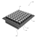
- FIG. 1 is a perspective view for explaining the overall outline of the electronic component mounting module 1000.
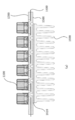
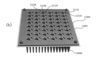
- the electronic component mounting module 1000 includes a first bus bar 1300, an insulating sheet 1400, and a second bus bar 1500 (not shown in FIG. 1), and a pedestal 1200 on the first bus bar 1300.
- a plurality of capacitors 1100 mounted on the surface are mounted on the surface.
- a heat sink 1600 is surface-mounted (surface contact) on the outer surface side of the second bus bar 1500.
- the bus bar laminated body can supply a large current and has excellent heat dissipation. Therefore, even if a large number of electronic components such as a capacitor 1100 are mounted at a high density, the electronic component It is possible to avoid thermal damage.
- the capacitor 1100 is known to be vulnerable to high heat, but the bus bar laminate of the present invention can maintain high reliability and high durability characteristics.
- Each of the bus bars 1300 and 1500 is made of a metal having a certain thickness in consideration of a large current and heat dissipation, and this makes it possible to obtain a considerably strong characteristic in terms of strength. Therefore, even a capacitor whose life is greatly affected by heat can be integrated without any problem.
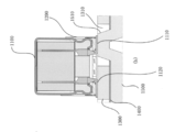
- the first electrode soldering convex body 1510 provided in the second bus bar 1500 is disposed in the convex body opening 1310 of the first bus bar 1300, and the first bus bar 1500 is provided with the first bus bar 1500.
- the outer surface of the bus bar 1300 has substantially the same height as reflow soldering is possible.
- the first lead terminal 1110 and the second lead terminal 1120 are inserted into the pedestal 1200 and bent at the bottom thereof, and the pedestal 1200 is set on the capacitor 1100 so that it can be handled as a surface mount type electronic component.
- the first lead terminal 1110 is reflow soldered to the flat top of the first electrode soldering convex body 1510.
- the height of the top of the first electrode soldering convex body 1510 and the plane of the peripheral edge of the convex body opening 1310 of the first bus bar 1300 can be made uniform. This makes it possible to use reflow solder easily.
- the first electrode solder convex body 1510 has a desired clearance in the convex body opening 1310 provided in the first bus bar 1300 at a position corresponding to the first electrode solder convex body 1510. It arrange
- the second lead terminal 1120 of the electronic component that is surface-mounted at the peripheral edge of the convex body opening 1310 is fixed by reflow soldering on the upper surface side of the paper. That is, the surface mount type electronic component shown in the present embodiment is reflow soldered on the mounting side. More specifically, in the bus bar laminated body of FIG. 3, an electronic component is surface-mounted on the upper surface of the first bus bar 1300 on the upper surface side of the paper, and the upper surface of the first bus bar 1300 on the upper surface side of the paper is reflow soldered.
- the lead terminal of the electronic component is fixed by soldering. As described above, each lead terminal is not inserted into and fixed to the bus bar, but is bent at the bottom of the base, mounted in surface contact, and soldered.
- Each of the bus bars 1300 and 1500 is formed of a metal having a considerable thickness, and is excellent in thermal conductivity and allows a large current to flow with low resistance. Due to the smooth heat dissipation effect of the bus bar laminate, thermal damage of a plurality of electronic components mounted on the bus bar laminate can be prevented.
- a convex body opening 1310 having a larger diameter is provided in the first bus bar 1300 at a location corresponding to the first electrode solder convex body 1510 provided in the second bus bar 1500. It is done.
- the second lead terminal 1120 of the surface mount electronic component mounted on the outer surface side of the first bus bar 1300 is electrically and mechanically reflow soldered to the first bus bar 1300 at the periphery of the convex body opening 1310.
- the insulating sheet 1200 may be formed by applying various insulating films (for example, a polyimide film) or an insulating material such as a resist.
- the opening area corresponding to the first electrode solder convex body 1510 of 1400 can be made smaller than the opening area of the convex body opening 1310.
- the solder cannot contact the bus bar 1500, and the insulation characteristics can be ensured reliably and safely.
- a resist agent or the like is applied to the side wall (tapered in FIGS.
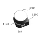
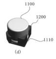
- FIGS. 4a, 4b, 4c, and 4d are diagrams illustrating a capacitor 1100 that is exemplified and mounted in the present embodiment configured as a surface mount type.
- a capacitor configuration is described as a typical example of an electronic component.
- the electronic component of the present invention is not limited to a capacitor, and may be any surface mount type electronic device. Good.
- the capacitor 1100 can be mounted by surface contact on the bottom surface of the pedestal 1200 by being fitted to the pedestal 1200 with the lead terminals 1110 and 1120 inserted therethrough.
- the first lead terminal 1110 and the second lead terminal 1120 are each inserted into the pedestal 1200 and bent along the bottom surface at the bottom surface, so that at least the tip portion protrudes from the edge of the pedestal 1200. . For this reason, when the capacitor 1100 and the pedestal 1200 are viewed from above, the front end portions of the first lead terminal 1110 and the second lead terminal 1120 are visible from the edge of the pedestal 1200.
- a pair of auxiliary terminals 1130 are provided on the bottom surface of the pedestal 1200 around the first lead terminal 1110 and the second lead terminal 1120, respectively. In the reflow soldering process, the first lead terminal 1110 and the second lead terminal 1120 are provided. By soldering each auxiliary terminal 1130 together with the two lead terminals 1120, the fixing strength is increased and the impact resistance and vibration resistance are improved.
- a part of the solder fillet for the first electrode 2110 is more preferably all formed in the flat top of the soldered convex body 1510 for the first electrode.
- the quality check and confirmation of the reflow soldering process can be carried out easily and quickly by observing and evaluating in plan view.
- the entire bottom surfaces of the first electrode 2110 and the second electrode 2120 are soldered, the mounting strength is increased, vibration resistance and impact resistance are improved, and thermal radiation characteristics are also improved. The reliability, durability, and life of the capacitor 2100 are improved.
- the external terminals of the surface mount component to be reflow soldered may be, for example, lead terminals exemplified in FIGS. 2a and 2b and electrode terminals exemplified in FIGS. 5a, 5b and 5c.
- the resin 1700 enters and fills the space around the first electrode soldering convex body 1510 and the convex body opening 1310.
- the overall strength is greatly increased, and vibration resistance, impact resistance and durability are improved.
- the capacitor 1100 is molded and integrated with the bus bars 1300 and 1500, so that the capacitor 1100 is fixed by the resin 1700, and the impact resistance is greatly improved.
- the bus bars 1300 and 1500 are not flat flat bus bars but have uneven shapes and increased surface areas, so that the contact area with the resin 1700 is increased.
- the heat dissipation characteristics and the adhesive strength can be increased. Even when large vibrations, impacts or accelerations are applied, the shape of the resin 1700 is maintained, so that the load on the lead terminals 1120 and 1110 is less than that when only the lead terminals 1120 and 1110 are fixed. That's it.
- the resin 1700 may be provided with an arbitrary path hole for venting the capacitor 1100.
- the resin 1700 may be molded with the heat sink 1600 provided.
- Capacitor 1110 .. First lead terminal, 1120 .. second lead terminal, 1130 .. Auxiliary terminal, 1200 ... pedestal, 1300 ... the first bus bar, 1310 .. Opening for convex body, 1400 .. Insulation sheet, 1500 ... second bus bar, 1510 .. Solder convex body for first electrode, 1600 ... Heat sink, 1700 .. Resin.
Landscapes
- Engineering & Computer Science (AREA)
- Power Engineering (AREA)
- Microelectronics & Electronic Packaging (AREA)
- Manufacturing & Machinery (AREA)
- Fixed Capacitors And Capacitor Manufacturing Machines (AREA)
- Structures For Mounting Electric Components On Printed Circuit Boards (AREA)
- Cooling Or The Like Of Semiconductors Or Solid State Devices (AREA)
- Structures Or Materials For Encapsulating Or Coating Semiconductor Devices Or Solid State Devices (AREA)
- Structure Of Printed Boards (AREA)
- Electric Connection Of Electric Components To Printed Circuits (AREA)
Priority Applications (3)
| Application Number | Priority Date | Filing Date | Title |
|---|---|---|---|
| CN202311006806.7A CN117292944A (zh) | 2018-06-05 | 2019-05-18 | 汇流条层叠体、具备该汇流条层叠体的电子部件安装模块、以及汇流条层叠体的制造方法 |
| CN201980037845.9A CN112219249A (zh) | 2018-06-05 | 2019-05-18 | 汇流条层叠体、具备该汇流条层叠体的电子部件安装模块、以及汇流条层叠体的制造方法 |
| EP19814797.7A EP3822997B1 (de) | 2018-06-05 | 2019-05-18 | Sammelschienenlaminat, modul zur montage elektronischer komponenten damit und verfahren zur herstellung eines sammelschienenlaminats |
Applications Claiming Priority (2)
| Application Number | Priority Date | Filing Date | Title |
|---|---|---|---|
| JP2018107427A JP7518601B2 (ja) | 2018-06-05 | 2018-06-05 | バスバー積層体及びそれを備える電子部品実装モジュール、バスバー積層体の製造方法 |
| JP2018-107427 | 2018-06-05 |
Publications (1)
| Publication Number | Publication Date |
|---|---|
| WO2019235189A1 true WO2019235189A1 (ja) | 2019-12-12 |
Family
ID=68770252
Family Applications (1)
| Application Number | Title | Priority Date | Filing Date |
|---|---|---|---|
| PCT/JP2019/019816 Ceased WO2019235189A1 (ja) | 2018-06-05 | 2019-05-18 | バスバー積層体及びそれを備える電子部品実装モジュール、バスバー積層体の製造方法 |
Country Status (4)
| Country | Link |
|---|---|
| EP (1) | EP3822997B1 (de) |
| JP (1) | JP7518601B2 (de) |
| CN (2) | CN112219249A (de) |
| WO (1) | WO2019235189A1 (de) |
Cited By (1)
| Publication number | Priority date | Publication date | Assignee | Title |
|---|---|---|---|---|
| EP4057785A1 (de) * | 2021-03-10 | 2022-09-14 | Rogers BV | Sammelschiene und verfahren zur herstellung einer sammelschiene |
Families Citing this family (2)
| Publication number | Priority date | Publication date | Assignee | Title |
|---|---|---|---|---|
| JP2023072794A (ja) * | 2021-11-15 | 2023-05-25 | 日本ケミコン株式会社 | バスバー積層体を備える電子部品実装モジュール及びその製造方法 |
| WO2025126705A1 (ja) * | 2023-12-12 | 2025-06-19 | 株式会社村田製作所 | コンデンサモジュール |
Citations (5)
| Publication number | Priority date | Publication date | Assignee | Title |
|---|---|---|---|---|
| JPH0626117U (ja) * | 1992-08-31 | 1994-04-08 | 日本メクトロン株式会社 | 内部端子型積層母線 |
| JPH10340630A (ja) * | 1998-05-20 | 1998-12-22 | Furukawa Electric Co Ltd:The | 内部端子付きバスプレート積層体 |
| JP2001178151A (ja) | 1999-12-20 | 2001-06-29 | Murata Mfg Co Ltd | インバータ用コンデンサモジュール、インバータ及びコンデンサモジュール |
| JP2006005096A (ja) * | 2004-06-16 | 2006-01-05 | Auto Network Gijutsu Kenkyusho:Kk | 回路構成体 |
| JP2009259915A (ja) * | 2008-04-14 | 2009-11-05 | Mitsubishi Electric Corp | 制御基板およびその製造方法、電気機器 |
Family Cites Families (15)
| Publication number | Priority date | Publication date | Assignee | Title |
|---|---|---|---|---|
| JP3322288B2 (ja) * | 1994-10-12 | 2002-09-09 | エルナー株式会社 | 電子部品およびその製造方法 |
| JP2005056954A (ja) * | 2003-07-31 | 2005-03-03 | Elna Co Ltd | 回路基板組立体およびチップ型電子部品 |
| US20070165376A1 (en) * | 2006-01-17 | 2007-07-19 | Norbert Bones | Three phase inverter power stage and assembly |
| JP2007265945A (ja) * | 2006-03-30 | 2007-10-11 | Tokyo R & D Co Ltd | ラミネートセル集積型バッテリ及びバッテリモジュール |
| DE502007003871D1 (de) * | 2007-09-28 | 2010-07-01 | Eberspaecher Controls Gmbh & C | Stromschiene mit Wärmeableitung |
| JP2010110170A (ja) * | 2008-10-31 | 2010-05-13 | Autonetworks Technologies Ltd | 回路構成体および電気接続箱 |
| TWI451817B (zh) * | 2011-05-26 | 2014-09-01 | 豐田自動織機股份有限公司 | 配線板及配線板的製造方法 |
| JP6044412B2 (ja) * | 2013-03-26 | 2016-12-14 | 株式会社オートネットワーク技術研究所 | リード端子と回路基板との接続構造、回路構成体及び電気接続箱 |
| JP6365186B2 (ja) * | 2014-09-29 | 2018-08-01 | 豊田合成株式会社 | バスバーモジュール |
| JP6274064B2 (ja) * | 2014-09-30 | 2018-02-07 | 豊田合成株式会社 | 電池モジュール |
| JP6467211B2 (ja) * | 2014-12-12 | 2019-02-06 | 日立オートモティブシステムズ株式会社 | 蓄電モジュール |
| JP6354600B2 (ja) * | 2015-01-16 | 2018-07-11 | 株式会社オートネットワーク技術研究所 | 回路構成体、電気接続箱及び回路構成体の製造方法 |
| CN105845440B (zh) * | 2016-04-11 | 2017-09-01 | 珠海英搏尔电气股份有限公司 | 交流电机控制器、电容阵列及其制作方法 |
| CN105680266B (zh) * | 2016-04-11 | 2017-11-03 | 珠海英搏尔电气股份有限公司 | 交流电机控制器、叠层母排组件及其制作方法 |
| CN206711772U (zh) * | 2017-04-27 | 2017-12-05 | 思源电气股份有限公司 | 一种超级电容模组结构 |
-
2018
- 2018-06-05 JP JP2018107427A patent/JP7518601B2/ja active Active
-
2019
- 2019-05-18 CN CN201980037845.9A patent/CN112219249A/zh active Pending
- 2019-05-18 CN CN202311006806.7A patent/CN117292944A/zh active Pending
- 2019-05-18 EP EP19814797.7A patent/EP3822997B1/de active Active
- 2019-05-18 WO PCT/JP2019/019816 patent/WO2019235189A1/ja not_active Ceased
Patent Citations (5)
| Publication number | Priority date | Publication date | Assignee | Title |
|---|---|---|---|---|
| JPH0626117U (ja) * | 1992-08-31 | 1994-04-08 | 日本メクトロン株式会社 | 内部端子型積層母線 |
| JPH10340630A (ja) * | 1998-05-20 | 1998-12-22 | Furukawa Electric Co Ltd:The | 内部端子付きバスプレート積層体 |
| JP2001178151A (ja) | 1999-12-20 | 2001-06-29 | Murata Mfg Co Ltd | インバータ用コンデンサモジュール、インバータ及びコンデンサモジュール |
| JP2006005096A (ja) * | 2004-06-16 | 2006-01-05 | Auto Network Gijutsu Kenkyusho:Kk | 回路構成体 |
| JP2009259915A (ja) * | 2008-04-14 | 2009-11-05 | Mitsubishi Electric Corp | 制御基板およびその製造方法、電気機器 |
Non-Patent Citations (1)
| Title |
|---|
| See also references of EP3822997A4 |
Cited By (1)
| Publication number | Priority date | Publication date | Assignee | Title |
|---|---|---|---|---|
| EP4057785A1 (de) * | 2021-03-10 | 2022-09-14 | Rogers BV | Sammelschiene und verfahren zur herstellung einer sammelschiene |
Also Published As
| Publication number | Publication date |
|---|---|
| EP3822997B1 (de) | 2025-07-09 |
| EP3822997A1 (de) | 2021-05-19 |
| CN112219249A (zh) | 2021-01-12 |
| JP2019212747A (ja) | 2019-12-12 |
| CN117292944A (zh) | 2023-12-26 |
| EP3822997A4 (de) | 2022-04-06 |
| JP7518601B2 (ja) | 2024-07-18 |
Similar Documents
| Publication | Publication Date | Title |
|---|---|---|
| CN103650082B (zh) | 电子部件 | |
| US10014111B2 (en) | Substrate terminal mounted electronic element | |
| CN102956353B (zh) | 芯片部件结构体及其制造方法 | |
| JP5083226B2 (ja) | 半導体装置およびその製造方法 | |
| EP2427040A1 (de) | Vorrichtung zur montage elektronischer komponenten und herstellungsverfahren dafür | |
| US20130223038A1 (en) | Module substrate and method for manufacturing module substrate | |
| TWI664881B (zh) | 零件模組 | |
| WO2019235189A1 (ja) | バスバー積層体及びそれを備える電子部品実装モジュール、バスバー積層体の製造方法 | |
| JP7199639B2 (ja) | バスバー積層体及びそれを備える電子部品実装モジュール、バスバー積層体の製造方法 | |
| US20240428996A1 (en) | Electronic component mounting module having bus bar stack, and method for manufacturing same | |
| JP2015141904A (ja) | 電子回路モジュール及びその製造方法 | |
| TWI403231B (zh) | 表面黏著型電路板件模組及其製法 | |
| US12288737B2 (en) | Thin semiconductor packaging unit having a plurality of bridging layers | |
| CN117894782A (zh) | 功率模块及其制备方法 | |
| JP7071707B2 (ja) | 電子部品実装モジュール及びその形成方法 | |
| JP2002190565A (ja) | ハイブリッドic及びその製造方法 | |
| US20260047001A1 (en) | Mounting substrate and mounting structure | |
| CN111902889B (zh) | 汇流条叠层板、该汇流条叠层板的电子元件安装模块及汇流条叠层板的制造方法 | |
| JP2020167311A (ja) | バスバー積層体及びそれを備える電子部品実装モジュール、電子部品実装モジュールの製造方法 | |
| JP3428083B2 (ja) | 半導体装置の製造方法 | |
| JP2023136446A (ja) | 部品モジュール | |
| JP2006005035A (ja) | 電子部品収納用セラミックパッケージ集合体およびセラミックパッケージ | |
| JP2003243562A (ja) | 樹脂封止基板とその製造方法および該基板中間製品とその製造方法 | |
| JPH04276689A (ja) | 集積回路実装基板 | |
| JPH10107177A (ja) | 表面実装用半導体パッケージ |
Legal Events
| Date | Code | Title | Description |
|---|---|---|---|
| 121 | Ep: the epo has been informed by wipo that ep was designated in this application |
Ref document number: 19814797 Country of ref document: EP Kind code of ref document: A1 |
|
| NENP | Non-entry into the national phase |
Ref country code: DE |
|
| ENP | Entry into the national phase |
Ref document number: 2019814797 Country of ref document: EP Effective date: 20210111 |
|
| WWG | Wipo information: grant in national office |
Ref document number: 2019814797 Country of ref document: EP |