WO2020003364A1 - Black matrix substrate and display device - Google Patents
Black matrix substrate and display device Download PDFInfo
- Publication number
- WO2020003364A1 WO2020003364A1 PCT/JP2018/024079 JP2018024079W WO2020003364A1 WO 2020003364 A1 WO2020003364 A1 WO 2020003364A1 JP 2018024079 W JP2018024079 W JP 2018024079W WO 2020003364 A1 WO2020003364 A1 WO 2020003364A1
- Authority
- WO
- WIPO (PCT)
- Prior art keywords
- layer
- conductive
- oxide
- thin film
- film transistor
- Prior art date
- Legal status (The legal status is an assumption and is not a legal conclusion. Google has not performed a legal analysis and makes no representation as to the accuracy of the status listed.)
- Ceased
Links
Images









Classifications
-
- G—PHYSICS
- G02—OPTICS
- G02F—OPTICAL DEVICES OR ARRANGEMENTS FOR THE CONTROL OF LIGHT BY MODIFICATION OF THE OPTICAL PROPERTIES OF THE MEDIA OF THE ELEMENTS INVOLVED THEREIN; NON-LINEAR OPTICS; FREQUENCY-CHANGING OF LIGHT; OPTICAL LOGIC ELEMENTS; OPTICAL ANALOGUE/DIGITAL CONVERTERS
- G02F1/00—Devices or arrangements for the control of the intensity, colour, phase, polarisation or direction of light arriving from an independent light source, e.g. switching, gating or modulating; Non-linear optics
- G02F1/01—Devices or arrangements for the control of the intensity, colour, phase, polarisation or direction of light arriving from an independent light source, e.g. switching, gating or modulating; Non-linear optics for the control of the intensity, phase, polarisation or colour
- G02F1/13—Devices or arrangements for the control of the intensity, colour, phase, polarisation or direction of light arriving from an independent light source, e.g. switching, gating or modulating; Non-linear optics for the control of the intensity, phase, polarisation or colour based on liquid crystals, e.g. single liquid crystal display cells
- G02F1/133—Constructional arrangements; Operation of liquid crystal cells; Circuit arrangements
- G02F1/1333—Constructional arrangements; Manufacturing methods
- G02F1/13338—Input devices, e.g. touch panels
-
- G—PHYSICS
- G02—OPTICS
- G02F—OPTICAL DEVICES OR ARRANGEMENTS FOR THE CONTROL OF LIGHT BY MODIFICATION OF THE OPTICAL PROPERTIES OF THE MEDIA OF THE ELEMENTS INVOLVED THEREIN; NON-LINEAR OPTICS; FREQUENCY-CHANGING OF LIGHT; OPTICAL LOGIC ELEMENTS; OPTICAL ANALOGUE/DIGITAL CONVERTERS
- G02F1/00—Devices or arrangements for the control of the intensity, colour, phase, polarisation or direction of light arriving from an independent light source, e.g. switching, gating or modulating; Non-linear optics
- G02F1/01—Devices or arrangements for the control of the intensity, colour, phase, polarisation or direction of light arriving from an independent light source, e.g. switching, gating or modulating; Non-linear optics for the control of the intensity, phase, polarisation or colour
- G02F1/13—Devices or arrangements for the control of the intensity, colour, phase, polarisation or direction of light arriving from an independent light source, e.g. switching, gating or modulating; Non-linear optics for the control of the intensity, phase, polarisation or colour based on liquid crystals, e.g. single liquid crystal display cells
- G02F1/133—Constructional arrangements; Operation of liquid crystal cells; Circuit arrangements
- G02F1/1333—Constructional arrangements; Manufacturing methods
- G02F1/1335—Structural association of cells with optical devices, e.g. polarisers or reflectors
- G02F1/133509—Filters, e.g. light shielding masks
- G02F1/133512—Light shielding layers, e.g. black matrix
-
- G—PHYSICS
- G02—OPTICS
- G02F—OPTICAL DEVICES OR ARRANGEMENTS FOR THE CONTROL OF LIGHT BY MODIFICATION OF THE OPTICAL PROPERTIES OF THE MEDIA OF THE ELEMENTS INVOLVED THEREIN; NON-LINEAR OPTICS; FREQUENCY-CHANGING OF LIGHT; OPTICAL LOGIC ELEMENTS; OPTICAL ANALOGUE/DIGITAL CONVERTERS
- G02F1/00—Devices or arrangements for the control of the intensity, colour, phase, polarisation or direction of light arriving from an independent light source, e.g. switching, gating or modulating; Non-linear optics
- G02F1/01—Devices or arrangements for the control of the intensity, colour, phase, polarisation or direction of light arriving from an independent light source, e.g. switching, gating or modulating; Non-linear optics for the control of the intensity, phase, polarisation or colour
- G02F1/13—Devices or arrangements for the control of the intensity, colour, phase, polarisation or direction of light arriving from an independent light source, e.g. switching, gating or modulating; Non-linear optics for the control of the intensity, phase, polarisation or colour based on liquid crystals, e.g. single liquid crystal display cells
- G02F1/133—Constructional arrangements; Operation of liquid crystal cells; Circuit arrangements
- G02F1/136—Liquid crystal cells structurally associated with a semi-conducting layer or substrate, e.g. cells forming part of an integrated circuit
- G02F1/1362—Active matrix addressed cells
- G02F1/136209—Light shielding layers, e.g. black matrix, incorporated in the active matrix substrate, e.g. structurally associated with the switching element
-
- G—PHYSICS
- G02—OPTICS
- G02F—OPTICAL DEVICES OR ARRANGEMENTS FOR THE CONTROL OF LIGHT BY MODIFICATION OF THE OPTICAL PROPERTIES OF THE MEDIA OF THE ELEMENTS INVOLVED THEREIN; NON-LINEAR OPTICS; FREQUENCY-CHANGING OF LIGHT; OPTICAL LOGIC ELEMENTS; OPTICAL ANALOGUE/DIGITAL CONVERTERS
- G02F1/00—Devices or arrangements for the control of the intensity, colour, phase, polarisation or direction of light arriving from an independent light source, e.g. switching, gating or modulating; Non-linear optics
- G02F1/01—Devices or arrangements for the control of the intensity, colour, phase, polarisation or direction of light arriving from an independent light source, e.g. switching, gating or modulating; Non-linear optics for the control of the intensity, phase, polarisation or colour
- G02F1/13—Devices or arrangements for the control of the intensity, colour, phase, polarisation or direction of light arriving from an independent light source, e.g. switching, gating or modulating; Non-linear optics for the control of the intensity, phase, polarisation or colour based on liquid crystals, e.g. single liquid crystal display cells
- G02F1/133—Constructional arrangements; Operation of liquid crystal cells; Circuit arrangements
- G02F1/136—Liquid crystal cells structurally associated with a semi-conducting layer or substrate, e.g. cells forming part of an integrated circuit
- G02F1/1362—Active matrix addressed cells
- G02F1/136286—Wiring, e.g. gate line, drain line
-
- G—PHYSICS
- G02—OPTICS
- G02F—OPTICAL DEVICES OR ARRANGEMENTS FOR THE CONTROL OF LIGHT BY MODIFICATION OF THE OPTICAL PROPERTIES OF THE MEDIA OF THE ELEMENTS INVOLVED THEREIN; NON-LINEAR OPTICS; FREQUENCY-CHANGING OF LIGHT; OPTICAL LOGIC ELEMENTS; OPTICAL ANALOGUE/DIGITAL CONVERTERS
- G02F1/00—Devices or arrangements for the control of the intensity, colour, phase, polarisation or direction of light arriving from an independent light source, e.g. switching, gating or modulating; Non-linear optics
- G02F1/01—Devices or arrangements for the control of the intensity, colour, phase, polarisation or direction of light arriving from an independent light source, e.g. switching, gating or modulating; Non-linear optics for the control of the intensity, phase, polarisation or colour
- G02F1/13—Devices or arrangements for the control of the intensity, colour, phase, polarisation or direction of light arriving from an independent light source, e.g. switching, gating or modulating; Non-linear optics for the control of the intensity, phase, polarisation or colour based on liquid crystals, e.g. single liquid crystal display cells
- G02F1/133—Constructional arrangements; Operation of liquid crystal cells; Circuit arrangements
- G02F1/136—Liquid crystal cells structurally associated with a semi-conducting layer or substrate, e.g. cells forming part of an integrated circuit
- G02F1/1362—Active matrix addressed cells
- G02F1/136286—Wiring, e.g. gate line, drain line
- G02F1/13629—Multilayer wirings
-
- G—PHYSICS
- G02—OPTICS
- G02F—OPTICAL DEVICES OR ARRANGEMENTS FOR THE CONTROL OF LIGHT BY MODIFICATION OF THE OPTICAL PROPERTIES OF THE MEDIA OF THE ELEMENTS INVOLVED THEREIN; NON-LINEAR OPTICS; FREQUENCY-CHANGING OF LIGHT; OPTICAL LOGIC ELEMENTS; OPTICAL ANALOGUE/DIGITAL CONVERTERS
- G02F1/00—Devices or arrangements for the control of the intensity, colour, phase, polarisation or direction of light arriving from an independent light source, e.g. switching, gating or modulating; Non-linear optics
- G02F1/01—Devices or arrangements for the control of the intensity, colour, phase, polarisation or direction of light arriving from an independent light source, e.g. switching, gating or modulating; Non-linear optics for the control of the intensity, phase, polarisation or colour
- G02F1/13—Devices or arrangements for the control of the intensity, colour, phase, polarisation or direction of light arriving from an independent light source, e.g. switching, gating or modulating; Non-linear optics for the control of the intensity, phase, polarisation or colour based on liquid crystals, e.g. single liquid crystal display cells
- G02F1/133—Constructional arrangements; Operation of liquid crystal cells; Circuit arrangements
- G02F1/136—Liquid crystal cells structurally associated with a semi-conducting layer or substrate, e.g. cells forming part of an integrated circuit
- G02F1/1362—Active matrix addressed cells
- G02F1/1368—Active matrix addressed cells in which the switching element is a three-electrode device
-
- G—PHYSICS
- G06—COMPUTING OR CALCULATING; COUNTING
- G06F—ELECTRIC DIGITAL DATA PROCESSING
- G06F3/00—Input arrangements for transferring data to be processed into a form capable of being handled by the computer; Output arrangements for transferring data from processing unit to output unit, e.g. interface arrangements
- G06F3/01—Input arrangements or combined input and output arrangements for interaction between user and computer
- G06F3/03—Arrangements for converting the position or the displacement of a member into a coded form
- G06F3/041—Digitisers, e.g. for touch screens or touch pads, characterised by the transducing means
-
- G—PHYSICS
- G06—COMPUTING OR CALCULATING; COUNTING
- G06F—ELECTRIC DIGITAL DATA PROCESSING
- G06F3/00—Input arrangements for transferring data to be processed into a form capable of being handled by the computer; Output arrangements for transferring data from processing unit to output unit, e.g. interface arrangements
- G06F3/01—Input arrangements or combined input and output arrangements for interaction between user and computer
- G06F3/03—Arrangements for converting the position or the displacement of a member into a coded form
- G06F3/041—Digitisers, e.g. for touch screens or touch pads, characterised by the transducing means
- G06F3/0412—Digitisers structurally integrated in a display
-
- G—PHYSICS
- G06—COMPUTING OR CALCULATING; COUNTING
- G06F—ELECTRIC DIGITAL DATA PROCESSING
- G06F3/00—Input arrangements for transferring data to be processed into a form capable of being handled by the computer; Output arrangements for transferring data from processing unit to output unit, e.g. interface arrangements
- G06F3/01—Input arrangements or combined input and output arrangements for interaction between user and computer
- G06F3/03—Arrangements for converting the position or the displacement of a member into a coded form
- G06F3/041—Digitisers, e.g. for touch screens or touch pads, characterised by the transducing means
- G06F3/044—Digitisers, e.g. for touch screens or touch pads, characterised by the transducing means by capacitive means
-
- G—PHYSICS
- G09—EDUCATION; CRYPTOGRAPHY; DISPLAY; ADVERTISING; SEALS
- G09F—DISPLAYING; ADVERTISING; SIGNS; LABELS OR NAME-PLATES; SEALS
- G09F9/00—Indicating arrangements for variable information in which the information is built-up on a support by selection or combination of individual elements
- G09F9/30—Indicating arrangements for variable information in which the information is built-up on a support by selection or combination of individual elements in which the desired character or characters are formed by combining individual elements
-
- H—ELECTRICITY
- H10—SEMICONDUCTOR DEVICES; ELECTRIC SOLID-STATE DEVICES NOT OTHERWISE PROVIDED FOR
- H10D—INORGANIC ELECTRIC SEMICONDUCTOR DEVICES
- H10D86/00—Integrated devices formed in or on insulating or conducting substrates, e.g. formed in silicon-on-insulator [SOI] substrates or on stainless steel or glass substrates
- H10D86/40—Integrated devices formed in or on insulating or conducting substrates, e.g. formed in silicon-on-insulator [SOI] substrates or on stainless steel or glass substrates characterised by multiple TFTs
- H10D86/421—Integrated devices formed in or on insulating or conducting substrates, e.g. formed in silicon-on-insulator [SOI] substrates or on stainless steel or glass substrates characterised by multiple TFTs having a particular composition, shape or crystalline structure of the active layer
- H10D86/423—Integrated devices formed in or on insulating or conducting substrates, e.g. formed in silicon-on-insulator [SOI] substrates or on stainless steel or glass substrates characterised by multiple TFTs having a particular composition, shape or crystalline structure of the active layer comprising semiconductor materials not belonging to the Group IV, e.g. InGaZnO
-
- H—ELECTRICITY
- H10—SEMICONDUCTOR DEVICES; ELECTRIC SOLID-STATE DEVICES NOT OTHERWISE PROVIDED FOR
- H10D—INORGANIC ELECTRIC SEMICONDUCTOR DEVICES
- H10D86/00—Integrated devices formed in or on insulating or conducting substrates, e.g. formed in silicon-on-insulator [SOI] substrates or on stainless steel or glass substrates
- H10D86/40—Integrated devices formed in or on insulating or conducting substrates, e.g. formed in silicon-on-insulator [SOI] substrates or on stainless steel or glass substrates characterised by multiple TFTs
- H10D86/451—Integrated devices formed in or on insulating or conducting substrates, e.g. formed in silicon-on-insulator [SOI] substrates or on stainless steel or glass substrates characterised by multiple TFTs characterised by the compositions or shapes of the interlayer dielectrics
-
- H—ELECTRICITY
- H10—SEMICONDUCTOR DEVICES; ELECTRIC SOLID-STATE DEVICES NOT OTHERWISE PROVIDED FOR
- H10D—INORGANIC ELECTRIC SEMICONDUCTOR DEVICES
- H10D86/00—Integrated devices formed in or on insulating or conducting substrates, e.g. formed in silicon-on-insulator [SOI] substrates or on stainless steel or glass substrates
- H10D86/40—Integrated devices formed in or on insulating or conducting substrates, e.g. formed in silicon-on-insulator [SOI] substrates or on stainless steel or glass substrates characterised by multiple TFTs
- H10D86/471—Integrated devices formed in or on insulating or conducting substrates, e.g. formed in silicon-on-insulator [SOI] substrates or on stainless steel or glass substrates characterised by multiple TFTs having different architectures, e.g. having both top-gate and bottom-gate TFTs
-
- H—ELECTRICITY
- H10—SEMICONDUCTOR DEVICES; ELECTRIC SOLID-STATE DEVICES NOT OTHERWISE PROVIDED FOR
- H10D—INORGANIC ELECTRIC SEMICONDUCTOR DEVICES
- H10D86/00—Integrated devices formed in or on insulating or conducting substrates, e.g. formed in silicon-on-insulator [SOI] substrates or on stainless steel or glass substrates
- H10D86/40—Integrated devices formed in or on insulating or conducting substrates, e.g. formed in silicon-on-insulator [SOI] substrates or on stainless steel or glass substrates characterised by multiple TFTs
- H10D86/60—Integrated devices formed in or on insulating or conducting substrates, e.g. formed in silicon-on-insulator [SOI] substrates or on stainless steel or glass substrates characterised by multiple TFTs wherein the TFTs are in active matrices
-
- H—ELECTRICITY
- H10—SEMICONDUCTOR DEVICES; ELECTRIC SOLID-STATE DEVICES NOT OTHERWISE PROVIDED FOR
- H10K—ORGANIC ELECTRIC SOLID-STATE DEVICES
- H10K50/00—Organic light-emitting devices
- H10K50/80—Constructional details
- H10K50/86—Arrangements for improving contrast, e.g. preventing reflection of ambient light
- H10K50/865—Arrangements for improving contrast, e.g. preventing reflection of ambient light comprising light absorbing layers, e.g. light-blocking layers
-
- H—ELECTRICITY
- H10—SEMICONDUCTOR DEVICES; ELECTRIC SOLID-STATE DEVICES NOT OTHERWISE PROVIDED FOR
- H10K—ORGANIC ELECTRIC SOLID-STATE DEVICES
- H10K59/00—Integrated devices, or assemblies of multiple devices, comprising at least one organic light-emitting element covered by group H10K50/00
- H10K59/40—OLEDs integrated with touch screens
Definitions
- the present invention relates to a black matrix substrate having a touch sensing function and a display device using the black matrix substrate.
- Touch-sensing functions include an on-cell method in which a touch panel is attached to a display surface such as a liquid crystal, micro LED (LED display in which minute LED chips are arranged in a matrix), organic EL (organic electroluminescence), and liquid crystal and organic EL.
- a touch panel is attached to a display surface such as a liquid crystal, micro LED (LED display in which minute LED chips are arranged in a matrix), organic EL (organic electroluminescence), and liquid crystal and organic EL.
- a touch sensing function is provided inside a display device.
- touch sensing using a pointer such as a finger or a pen
- fingerprint authentication by detecting unevenness of a fingerprint, pen input, feather touch input (light touch input close to non-contact)
- touch sensing that can perform various detections such as touch input that applies a large pressing force to the substrate and has a wide allowable range of the pressing force to the substrate.
- a self-capacitance type touch sensing method and a mutual capacitance type touch sensing method are known.
- the self-capacitance type touch sensing method uses an individual electrode pattern in which a plurality of electrodes and the like formed of a transparent conductive film such as ITO are formed independently of each other. This is a detection method.
- the mutual capacitance type touch sensing method is a method of arranging touch sensing wires (hereinafter abbreviated as touch wires) in an X direction and a Y direction, and detecting a capacitance generated between the X direction wires and the Y direction wires. It is.
- the in-cell system has a structure in which touch wiring is formed at a position close to a display function layer such as a liquid crystal layer, unlike a touch panel externally attached to a display device.
- the in-cell method does not require an extra member such as a touch panel, so that a thin and lightweight display device or electronic device can be provided.
- the touch wiring is provided at a position close to a display function layer such as a liquid crystal layer. Therefore, a parasitic capacitance is easily generated between a wiring such as a gate wiring and a source wiring forming a thin film transistor for driving the display function layer and the touch wiring, and the thin film transistor is easily affected by noise.
- touch input with a pen touch input with a pen, or fingerprint authentication in addition to touch input with a finger
- the same number of pixels as a high-definition liquid crystal display device for example, 2400 pixels ⁇ 1200 pixels is required.
- a structure in which the wiring density of a plurality of touch wirings extended in each of the X direction and the Y direction is required. This structure can be applied to a narrow frame structure that increases the area of the effective display screen.
- a tablet terminal or the like in which an electromagnetic induction sensor substrate is disposed in a display device and performs pen input on a display surface of the display device using a stylus pen having a battery is commercially available. I have. However, there is a problem that an extra member such as an electromagnetic induction sensor board and a stylus pen is required for the electromagnetic induction pen input.
- Patent Literature 1 discloses a fingerprint input device using MOS-FETs arranged in a lattice. However, Patent Document 1 does not disclose a touch panel configuration formed on a transparent substrate.
- Patent Document 2 discloses a liquid crystal display device to which a touch sensing technology using a plurality of transistors is applied.
- the sensor circuit 45 includes the transistor M3 and the capacitor CS1.
- the electrode ECS overlaps with the electrode COM
- the electrode CS1 includes the electrode ECS, the electrode COM, and the insulating layer 65.
- the electrodes ECS and the electrodes COM are light-transmitting conductive films, and have complicated structures. In the case where the electrodes ECS and the electrodes COM are formed of a light-transmitting conductive film in a display device that performs liquid crystal driving, another problem occurs. This will be described later.
- each of the first block, which is the main part of the first line, and the second block, which is the main part of the second line is formed by patterning a transparent conductive layer. It is formed with.
- the transparent conductive layer include ITO, IZO, and ITZO.
- the technology disclosed in Patent Literature 3 can be rephrased as a mutual capacitance type touch sensing technology for detecting a change in capacitance between the first line and the second line.
- a pattern forming step for the first line and the second line and a pattern forming for the second bridge are required, and the forming step is complicated.
- the main part of the first line and the second line is a transparent conductive layer having a high resistance value, so that touch sensing with a large time constant is performed, which is not preferable.
- the response of the touch signal is slow, and it is difficult to expect a high S / N ratio (ratio between signal and noise).
- the first block and the second block are transparent conductive layers (or light-transmitting conductive films), there is another problem. This will be described later.
- Patent Document 4 discloses a touch sensing technology in which one of a pair of wirings functions as a detection wiring and the other functions as a driving wiring, as disclosed in claim 17.
- the disclosure of FIG. 4, FIG. 5, and paragraph [0108] of Patent Document 4 are typical wiring examples.
- Patent Documents 3 and 4 both disclose a mutual capacitance type touch sensing technology.
- Patent Document 4 does not disclose a conductive pattern having a configuration in which a copper layer or a copper alloy layer is sandwiched between conductive oxides, and a conductive pattern is used for a capacitor pattern having one or more openings. No disclosed structure is disclosed, nor is a structure in which a capacitor pattern extends to form a gate electrode of a thin film transistor.
- the present invention has been made in view of the above problems, and in addition to general touch sensing using a pointer such as a finger or a pen, has a touch sensing function capable of performing fingerprint authentication and the like by detecting the uneven shape of a fingerprint.
- a black matrix substrate provided with the same, and a display device using the black matrix substrate.
- the present invention provides a black matrix substrate having a simple configuration without using a transparent conductive film (transparent electrode) and without using an extra member.
- a black matrix substrate includes a transparent substrate having a first surface and a second surface, a black dielectric layer provided on the second surface, and a black dielectric layer provided on the black dielectric layer.
- a second conductive layer including a second conductive pattern having a configuration in which the layer is sandwiched between conductive oxide layers; a transparent resin layer provided on the second conductive pattern; and a second conductive layer provided on the transparent resin layer.
- Light absorbing layer, first gate electrode, first source electrode, first drain A first thin film transistor having a pole, a first channel layer, and a gate insulating layer, wherein the black dielectric layer contains carbon, and the first conductive pattern and the first conductive pattern when viewed in a plan view from the first surface.
- the light absorbing layer has a configuration that covers the second conductive pattern, the light absorbing layer includes carbon, and has a configuration that covers the first conductive pattern and the second conductive pattern in plan view as viewed from the second surface.
- a part of the first conductive pattern forms the first gate electrode; a part of the second conductive pattern forms the first source electrode and the first drain electrode; Part of the layer constitutes the first channel layer, part of the first conductive pattern constitutes a scanning line for driving the first thin film transistor, and part of the second conductive pattern constitutes the first channel layer.
- 1 thin film A part of the first conductive pattern forms a capacitor pattern connected to the first gate electrode, and the capacitor pattern has one or more first openings in plan view. And a part of the second insulating layer constitutes the gate insulating layer.
- the black matrix substrate according to the first aspect of the present invention includes a second gate electrode electrically connected to the first gate electrode, a second source electrode, a second drain electrode electrically connected to the second gate electrode, and a second gate electrode.
- a second thin film transistor having a channel layer and a gate insulating layer, wherein a part of the first conductive pattern forms the second gate electrode, and a part of the second conductive pattern includes the second source electrode and The second drain electrode is formed, a part of the oxide semiconductor layer forms the second channel layer, and a part of the second insulating layer forms the gate insulating layer of the second thin film transistor. You may.
- the scanning lines extend in parallel to the first direction
- the output lines extend in parallel to a second direction orthogonal to the first direction.
- the capacitor pattern may be disposed in a region defined by the scanning line and the output line.
- the first opening is an opening having a rectangular or parallelogram shape
- each of the black dielectric layer and the light absorbing layer is A second opening having a rectangular shape or a parallelogram similar to the opening may be provided, and a center position of the second opening may overlap a center position of the first opening.
- the black dielectric layer may be a resin dispersion containing carbon and dielectric fine particles made of at least a metal oxide.
- the dielectric composed of the metal oxide includes one or more paraelectric fine particles selected from the group consisting of forsterite, aluminum oxide, and titanium oxide. It may include at least.
- the black dielectric layer may include carbon and at least one or more fine particles selected from the group consisting of titanium oxide, titanium nitride, and titanium oxynitride. Good.
- the black dielectric layer is composed of two layers of resin dispersions having different carbon concentrations, and at least one of the two layers of resin dispersions is made of resin.
- the dispersion may include a dielectric composed of a metal oxide.
- the conductive oxide layer may include indium oxide.
- the oxide semiconductor layer may include indium oxide and at least one of antimony oxide and bismuth oxide.
- the oxide semiconductor layer may include at least one of cerium oxide and tin oxide.
- a display device includes the black matrix substrate according to the first aspect, an array substrate having a substrate surface on which a thin film transistor array is arranged, and a display function layer, and a display function layer interposed therebetween. Then, the second surface of the black matrix substrate and the substrate surface of the array substrate are attached to each other so as to face each other.
- the black matrix substrate having a touch sensing function capable of performing fingerprint authentication or the like by detecting the uneven shape of a fingerprint
- the black matrix Provided is a display device using a substrate. Further, it is possible to provide a black matrix substrate having a simple structure without using a transparent conductive film (transparent electrode) and without using an extra member.
- FIG. 2 is a partially enlarged view showing a configuration of the black matrix substrate according to the first embodiment of the present invention, and is a circuit diagram showing a sensor unit (unit cell) including a capacitor pattern and a thin film transistor (first thin film transistor).
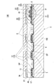
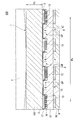
- FIG. 2 is a cross-sectional view showing the sensor unit along the line A-A ′ shown in FIG. 1.
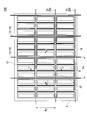
- FIG. 2 is a partially enlarged view showing the configuration of the black matrix substrate according to the first embodiment of the present invention, in which a first conductive pattern of a first conductive layer and a second conductive layer of a second conductive layer disposed on a black dielectric layer. It is a top view showing arrangement of a pattern.
- FIG. 1 is a partially enlarged view showing a configuration of the black matrix substrate according to the first embodiment of the present invention, and is a circuit diagram showing a sensor unit (unit cell) including a capacitor pattern and a thin film transistor (first thin film transistor).
- FIG. 2 is a cross-sectional view showing the sensor unit along
- FIG. 4 is a cross-sectional view showing the sensor unit along the line B-B ′ shown in FIG. 3.
- FIG. 4 is a sectional view showing the sensor unit along the line C-C ′ shown in FIG. 3.
- FIG. 2 is a partially enlarged view showing the black matrix substrate according to the first embodiment of the present invention, and is a cross-sectional view showing a structure of a conductive layer provided on a first insulating layer on a black dielectric layer.
- FIG. 2 is a partially enlarged view illustrating a configuration of the black matrix substrate according to the first embodiment of the present invention, and is a cross-sectional view illustrating a situation when a pointer such as a finger contacts the first surface of the black matrix substrate.
- FIG. 9 is a view showing a black matrix substrate according to a modification of the first embodiment of the present invention, wherein a layer of a resin dispersion having a different carbon concentration is inserted between a second surface and a black dielectric layer; It is sectional drawing explaining the situation of reflection of visible light. It is a circuit diagram showing a sensor unit which constitutes a black matrix board concerning a modification of a 1st embodiment of the present invention. It is a circuit diagram showing a sensor unit which constitutes a black matrix board concerning a modification of a 1st embodiment of the present invention.
- FIG. 4 is a partially enlarged view showing a black matrix substrate according to a modification of the first embodiment of the present invention, in which a first conductive pattern of a first conductive layer and a second conductive pattern of a second conductive layer are provided on a black dielectric layer. It is a top view showing arrangement of a conductive pattern.
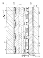
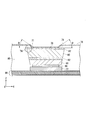
- FIG. 6 is a diagram illustrating a display device according to a second embodiment of the present invention, and is a cross-sectional view partially illustrating a micro LED display device to which the black matrix substrate according to the first embodiment of the present invention is applied.
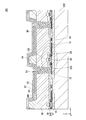
- FIG. 9 is a view showing a display device according to a second embodiment of the present invention, and is a partial cross-sectional view of an array substrate on which micro LEDs are mounted.
- FIG. 6 is a diagram illustrating a display device according to a second embodiment of the present invention, and is a cross-sectional view partially illustrating a micro LED display device to which the black matrix substrate according to the first embodiment of the present invention is applied
- FIG. 14 is a diagram illustrating a display device according to a second embodiment of the present invention, and is an enlarged cross-sectional view of a region indicated by reference numeral C in FIG. 13.
- FIG. 14 is a diagram illustrating a display device according to a second embodiment of the present invention, and is an enlarged cross-sectional view of a first thin film transistor illustrated in FIG. 13.
- FIG. 9 is a typical circuit diagram including a thin film transistor that drives a micro LED applied to a display device according to a second embodiment of the present invention. It is a figure showing the display concerning a 3rd embodiment of the present invention, and is a sectional view showing a part of an organic EL display to which a black matrix substrate was applied.
- FIG. 14 is a diagram illustrating a display device according to a second embodiment of the present invention, and is an enlarged cross-sectional view of a region indicated by reference numeral C in FIG. 13.
- FIG. 14 is a diagram illustrating a display device according to a second embodiment
- FIG. 10 is a view showing a display device according to a third embodiment of the present invention, and is a partial cross-sectional view of an array substrate on which an organic EL layer is mounted. It is a figure showing the display concerning a 4th embodiment of the present invention, and is a sectional view showing a liquid crystal display to which a black matrix substrate is applied partially.
- FIG. 13 is a typical circuit diagram including a thin film transistor for driving a liquid crystal layer applied to a display device according to a fourth embodiment of the present invention.
- FIG. 4 is a cross-sectional view partially showing a liquid crystal display device employing a conventional horizontal alignment liquid crystal (FFS mode), showing the state of equipotential lines when a liquid crystal driving voltage is applied between a pixel electrode and a common electrode.
- FFS mode horizontal alignment liquid crystal
- FIG. 2 is a cross-sectional view partially showing a liquid crystal display device employing a conventional horizontal alignment liquid crystal (FFS mode), illustrating the state of equipotential lines when a transparent electrode is provided on a transparent resin layer of a substrate. It is sectional drawing.
- FFS mode horizontal alignment liquid crystal
- the phrase “in a plan view from the first surface” refers to a black dielectric layer, a conductive pattern, and a light absorption layer laminated on a second surface (back surface) of a transparent substrate, which are defined by an observer. It means a plan view seen from the first surface. Further, the phrase “in a plan view from the second surface” means that the conductive pattern and the black dielectric layer laminated on the second surface of the transparent substrate are separated from the second surface (the surface opposite to the viewer's view surface). Means a planar view as seen. When the wording “plan view viewed from the first surface” and the word “plan view viewed from the second surface” are substantially equivalent, they are simply referred to as “plan view”.
- first and second are used to avoid confusion between components, and do not limit the number.
- the first conductive pattern and the second conductive pattern may be simply referred to as a conductive pattern or a conductive layer.
- Each of the conductive layers (conductive patterns) has a three-layer structure in which a metal layer or an alloy layer is sandwiched between conductive oxide layers.
- the “display function layer” included in the display device includes a plurality of light-emitting diode elements called LEDs (Light Emitting Diodes) and a plurality of organic ELs (organic electroluminescence) also called OLEDs. Either an element or a liquid crystal layer can be used.
- FIG. 1 is a partially enlarged view showing the configuration of the black matrix substrate according to the first embodiment of the present invention, and is a circuit diagram showing a sensor unit (unit cell) including a capacitor pattern and a thin film transistor (first thin film transistor).
- the minimum element configuration is shown as the configuration of the partition region 19 for easy understanding. That is, FIG. 1 illustrates a minimum element configuration including only one first thin film transistor 31 in the partitioned area 19.
- FIG. 1 shows a circuit diagram, an actual configuration in which the capacitor pattern 12 is formed by the three openings 9, that is, a schematic configuration of the sensor unit, for easy understanding of the following description. Is shown.
- the capacitor pattern 12 is provided in a partition region 19 (region) partitioned by the scanning lines and the output lines.
- the partition region 19 is a region partitioned by the scanning line 13 for driving the thin film transistor and the output line 21 to which an output signal is applied from the thin film transistor.
- a sensor including a conductive layer (conductive pattern) in which a black dielectric layer, a metal layer or an alloy layer is sandwiched between conductive oxides, a light absorbing layer, a thin film transistor, a single capacitor pattern, and the like.
- a unit is defined as a unit cell.
- a plurality of unit cells are arranged in a matrix on a black matrix substrate.
- a sensor unit or a unit cell may be used as a technical term in the description.
- the sensor unit or the unit cell has the same meaning as a region where a capacitor is formed, that is, a region defined by a scanning line and an output line. In plan view, the scanning lines extend parallel to the first direction, and the output lines extend parallel to a second direction orthogonal to the first direction.
- the sensor unit SU includes a first conductive pattern 10, a second conductive pattern 20, and a first thin film transistor 31.
- the first thin film transistor 31 includes a first gate electrode 11, a first source electrode 22, a first drain electrode 23, a first channel layer 16 (described later, an oxide semiconductor layer), and a gate insulating layer (described later, a second insulating layer 48). ).
- the first source electrode 22 is connected to the scanning line 13 via a contact hole 29.
- the first drain electrode 23 is connected to the output line 21.
- the first drain electrode 23 is connected to the output line 21.
- the output line 21, the first source electrode 22, and the first drain electrode 23 form the second conductive pattern 20.
- the second conductive pattern 20 is formed of the second conductive layer
- the first conductive pattern 10 is formed of the first conductive layer.
- the first conductive pattern 10 and the second conductive pattern 20 may be simply referred to as a conductive pattern.
- the first conductive layer and the second conductive layer may be simply referred to as a conductive layer.
- the conductive layer refers to a structure in which a metal layer or an alloy layer is sandwiched between conductive oxide layers, as described later.
- the first gate electrode 11, the capacitor pattern 12 (capacitor electrode), and the scanning line 13 form a first conductive layer having the first conductive pattern 10.
- the capacitor pattern 12 includes one or more openings 9 (first openings) in plan view.
- the shape of the opening 9 is not limited to the rectangle shown in FIG. 1 and may be a parallelogram.
- the capacitor pattern 12 is connected to the first gate electrode 11.
- the capacitor pattern 12 supplies a change in capacitance when a pointer such as a finger contacts or approaches the first surface 1 to the first thin film transistor 31 as a signal.
- the capacitor pattern 12 may be referred to as a capacitor electrode.
- reference characters R, G, and B denote red pixels R of an array substrate facing (attached to) the black matrix substrate when the black matrix substrate is applied to a display device that performs color display. , Green pixel G, and blue pixel B, respectively. That is, the capacitor pattern 12 has a size corresponding to the size of one or more pixels used for display. For example, in the case of displaying an image using three pixels of red, green, and blue, the size of the capacitor pattern may be an integral multiple of three. For example, in the case of displaying an image using four pixels of red, green, blue, and white, the size of the capacitor pattern can be set to an integral multiple of four. In a fourth embodiment described later, a configuration in which a color filter including a red pixel, a green pixel, and a blue pixel is arranged in the opening 9 of the black matrix substrate is illustrated.
- the output line 21, the first source electrode 22, and the first drain electrode 23 form a second conductive layer having the second conductive pattern 20.
- the roles (functions) of the scanning line and the output line can be switched. Further, the roles (functions) of the source electrode and the drain electrode can be interchanged. That is, in FIG. 1, reference numeral 13 may be an output line, reference numeral 21 may be a scanning line, reference numeral 22 may be a first drain electrode, and reference numeral 23 may be a first source electrode.
- the first conductive layer and the second conductive layer have a configuration in which a metal layer or an alloy layer is sandwiched between conductive oxide layers. Since the first gate electrode 11, the capacitor pattern 12, the scanning line 13, and the output line 21 forming the second conductive layer, which constitute the first conductive layer, are made of a metal or alloy having excellent conductivity, they are static. The responsiveness of the capacitance detection and the S / N ratio can be improved. Examples of the metal having high conductivity as described above include silver, copper, and aluminum. In consideration of reliability, a silver alloy, a copper alloy, or an aluminum alloy may be used. By using a conductive layer (conductive pattern) in which a metal layer or an alloy layer is sandwiched between conductive oxide layers as a configuration of the capacitor pattern 12, the scanning line 13, and the output line 21, a plurality of advantages described below can be obtained. Can be
- the capacitance of a pointer such as a finger is large.
- electrostatic breakdown may occur, and chipping or peeling of the copper alloy wiring may occur.
- silver, copper, or a copper alloy has insufficient adhesion to resin or glass.
- a conductive layer in which a metal layer or an alloy layer is sandwiched between conductive oxide layers is employed.
- the conductive oxide has extremely high adhesion to silver, copper, a copper alloy, or the like, and further has extremely high adhesion to resin or glass. Therefore, chipping or peeling of the copper alloy wiring due to electrostatic breakdown hardly occurs.
- Second advantage For example, when silver alloy wiring or copper alloy wiring is adopted as the structure of the conductive layer (in the case of using no conductive oxide), silver or copper diffuses into the resin or glass base material, and the reliability is improved. May cause a decrease. In particular, when the manufacturing process includes a processing step exceeding 250 ° C., copper or a copper alloy is easily oxidized. In contrast, when a conductive layer in which a metal layer or an alloy layer is sandwiched between conductive oxide layers is employed as in the present embodiment, the conductive oxide layer diffuses silver or copper into the glass substrate. Inhibits copper oxidation.
- Silver, copper, or copper alloys are relatively soft metals. For this reason, the wiring made of silver, copper, or a copper alloy is easily damaged during electrical mounting at the end of the touch panel.
- the conductive oxide is also one of the ceramic materials. When the oxide layer sandwiches copper, a silver alloy, or a copper alloy, hard and reliable mounting becomes possible.
- the first source electrode 22 is electrically connected to the scanning line 13 via the contact hole 29.
- a good electrical connection in the contact hole 29 is obtained by the conductive oxide layer.
- a copper oxide is easily formed on the surface of copper or a copper alloy. Copper oxide increases in thickness over time, making electrical packaging unstable. Similarly, oxides and sulfides are easily formed on the surface of silver. In a configuration in which copper or a copper alloy is sandwiched between conductive oxide layers, a conductive oxide layer is formed on the surface of the conductive layer (conductive pattern), and ohmic contact is possible.
- the conductive layer according to the embodiment of the present invention can be applied to a source wiring, a source electrode, a drain electrode, a gate electrode, a gate wiring, and a touch sensing wiring of various TFTs (thin film transistors).
- a mixed oxide containing at least 50 at% of indium oxide can be used.
- a method for forming a three-layer structure in which a copper layer or a copper alloy layer is sandwiched between two conductive oxide layers first, for example, a method in which [mixed oxide layer A / copper alloy layer B / mixed oxide layer C]. Thereafter, the three layers are processed so as to have the same line width by a wet etching process.
- the line width of the mixed oxide layer A, the copper alloy layer B, and the mixed oxide layer C sequentially formed on the surface of the glass substrate by the wet etching process is set to satisfy the condition “line width of mixed oxide layer A>
- line width of mixed oxide layer C In order to satisfy “line width of copper alloy layer B> line width of mixed oxide layer C”, it is necessary to process so that the line width becomes smaller in order.
- ITO mixed oxide containing indium oxide and tin oxide
- copper is selectively etched, and the line width of the three layers does not satisfy the above condition. Therefore, by adding a readily soluble oxide such as zinc oxide, gallium oxide, and antimony oxide to indium oxide, the corrosion potential is adjusted, and a mixed oxide layer having a uniform corrosion potential is obtained.
- the conductive layers (the first conductive layer and the second conductive layer) according to the embodiment of the present invention have a three-layer structure in which the metal layer or the alloy layer is sandwiched between the conductive oxides as described above.
- a metal such as silver, copper, aluminum, or zinc having excellent conductivity, or an alloy layer of the above metals can be used.
- copper and a copper alloy will be described as typical examples, but the basic technical means according to the embodiment of the present invention can also be applied to metals such as silver and zinc.
- an alloy element to be added to copper an alloy element whose specific resistance increase rate of the copper alloy layer is 1 ⁇ cm / at% or less can be selected.
- the specific resistance (electrical resistivity) of the copper alloy layer can be in the range of 1.9 ⁇ cm to 6 ⁇ cm.
- Zinc and calcium can each be added as alloying elements to copper up to 5 at%.
- the conductive layer hardly transmits visible light. Therefore, if the copper layer or the copper alloy layer constituting the conductive layer according to the present embodiment has a thickness of, for example, 100 nm to 500 nm, sufficient light-shielding properties can be obtained.
- the thickness of the copper alloy layer may exceed 500 nm.
- the material of the conductive layer can be applied to wirings and electrodes provided on an array substrate described later.
- a structure of a wiring electrically linked to an active element for example, as a structure of a gate electrode or a gate wiring, a stacked structure in which a copper alloy layer is sandwiched between conductive metal oxide layers.
- a structure can be adopted.
- a laminated structure in which a copper alloy layer is sandwiched between conductive metal oxide layers can be adopted for the conductive layer (conductive pattern) according to the embodiment of the present invention.
- FIG. 2 is a cross-sectional view showing the sensor unit SU (unit cell) along the line AA ′ shown in FIG. FIG. 2 can be restated as a cross-sectional view showing the black matrix substrate 100 according to the embodiment of the present invention.
- the black matrix substrate 100 has a transparent substrate 102 (first substrate) having a first surface 1 and a second surface 2.
- the specific substrate material of the transparent substrate 102 that can be used for the black matrix substrate 100 is not particularly limited as long as it is a material that is transparent in the visible region.
- Various transparent substrates such as sapphire substrates, substrates made of aluminosilicate glass, etc., acrylic substrates, polyester films, polyimide films, TAC films used for polarizing plates, and resin substrates laminated with vinyl chloride used for IC cards Can be used.
- the substrate be a rigid substrate, such as a glass substrate, having a highly planar and highly flat surface.
- the black dielectric layer 3 and the first insulating layer 17 are laminated in this order. That is, the black dielectric layer 3 is provided on the second surface 2, and is formed on the black dielectric layer 3 so as to cover the exposed surface (surface) of the second surface 2 and the surface of the black dielectric layer 3.
- a first insulating layer 17 is provided. Further, a first conductive pattern 10 is provided on the first insulating layer 17.
- the second insulating layer 48 is laminated so as to cover the first conductive pattern 10 (including the first gate electrode 11, the capacitor pattern 12, and the scanning line 13) and the exposed surface (surface) of the first insulating layer 17. That is, the second insulating layer 48 is provided on the first conductive pattern 10.
- a first transparent resin layer 37 (transparent resin layer) is provided on the second insulating layer 48. That is, a transparent resin layer is provided on the second conductive pattern 20 (second conductive layer).
- a light absorbing layer 8 and a second transparent resin layer 38 are laminated on the first transparent resin layer 37.
- the second transparent resin layer 38 covers the exposed surface (surface) of the first transparent resin layer 37 and the light absorbing layer 8.
- First insulating layer As a material of the first insulating layer 17, as described later, silicon dioxide, silicon nitride, or a transparent inorganic oxide or transparent nitride having a high dielectric constant can be applied.
- a material of the first transparent resin layer 37 or the second transparent resin layer 38 an acrylic resin, a polyimide resin, a benzocyclobutene resin, a polyamide resin, or the like may be used.
- a low dielectric material low-k material
- a conductor layer having the same pattern as the first transparent resin layer 37 in plan view may be inserted. This conductor layer may be grounded as necessary to form an auxiliary capacitance between the conductor layer and the capacitor pattern 12.
- the first insulating layer 17 may have a thickness of, for example, 1 nm to 1000 nm.
- the material of the first insulating layer 17 may be an oxide layer containing one or more of silicon dioxide, silicon oxynitride, cerium oxide, and titanium oxide.
- the first insulating layer 17 may be formed of a material having a high dielectric constant at an interface between the capacitor pattern 12 and the first insulating layer 17.
- a material constituting the first insulating layer 17 is not particularly limited, and examples thereof include silicon oxide, silicon oxynitride, and silicon nitride.
- the thickness of the first insulating layer 17 does not need to be limited, but may be, for example, in the range of 1 nm to 1000 nm.
- the black dielectric layer 3 contains carbon.
- the black dielectric layer 3 is composed of a dispersion in which carbon is dispersed in a resin, or a dispersion in which a dielectric which is fine particles of metal oxide or the like is further dispersed in carbon. That is, the black dielectric layer 3 may be composed of a resin dispersion containing carbon and dielectric fine particles composed of at least a metal oxide.
- the black dielectric layer 3 has a configuration that covers the first conductive pattern 10 and the second conductive pattern 20 in plan view. In the following description, the fine particles may be simply referred to as powder.
- the electrical characteristics of the black dielectric layer 3 are adjusted so as to have a high relative dielectric constant of, for example, 10 to 700. It is possible to do.
- the relative dielectric constant of the black dielectric layer 3 can be adjusted to 150 or more by adjusting the dispersion state of carbon or adding fine particles of a ferroelectric substance or fine particles of a paraelectric substance to the black dielectric layer 3. it can.
- the black matrix substrate according to the present embodiment is applied to an electronic device in which an increase in power consumption is a problem due to the dielectric loss (tan ⁇ ) of the black dielectric layer 3 (for example, a mobile device), the black dielectric layer 3 May be suppressed in the range of 15 to 100.
- the black matrix substrate 100 has a configuration in which the black dielectric layer 3 is inserted between the second surface 2 of the transparent substrate 102 and the capacitor pattern 12.
- a material constituting the black dielectric layer 3 according to the embodiment of the present invention a dispersion in which carbon as a black pigment is dispersed in a resin such as acryl, epoxy, or polyimide can be used. Further, carbon nanotubes, carbon nanohorns, carbon nanobrushes and the like may be mixed and dispersed in the resin. Alternatively, a part of the configuration of the black dielectric layer 3 may be replaced with carbon, and the carbon nanotubes may be dispersed in the resin.
- the black dielectric layer 3 may be simply referred to as a black dielectric.
- the black dielectric layer 3 includes calcium oxide, calcium carbonate, barium sulfate, and silicon dioxide for the purpose of adjusting the dispersion state of carbon and adjusting the relative dielectric constant.
- An extender such as kaolin, clay or the like can be added to the black dielectric layer 3.
- a resin dispersion to which a dielectric powder having a high dielectric constant such as titanium oxide, barium titanate, titanium black, barium zirconate, magnesium titanate, or calcium sulfate is added in addition to carbon. it can.
- a dispersion of a resin to which a dielectric powder containing any of titanium oxide, titanium nitride, and titanium oxynitride in addition to carbon can be used.
- a paraelectric for the purpose of improving the dispersion state of carbon in the black dielectric layer 3 and not increasing the dielectric loss.
- the paraelectric has no electric polarization when no electric field is applied, and has a small dielectric loss.
- a metal oxide such as forsterite (MgSiO 2 ), aluminum oxide (Al 2 O 3 ), or titanium oxide (TiO 2 ), which is a paraelectric, can be added to the black dielectric.
- the dielectric constant of a black dielectric obtained by adding a ferroelectric substance to a resin is increased, but the power consumption is increased in the touch drive for performing touch detection.
- a black dielectric obtained by adding a paraelectric substance to a resin and dispersing the resin can increase the amount of change in the capacitance (difference between the capacitance at the time of reset and the capacitance at the time of touch) and suppress power consumption.
- the paraelectric metal oxide is a metal oxide or a metal oxide powder having a relative dielectric constant of 110 or less and a dielectric loss in a range of 0.00001 to 0.1. Define.
- the measurement frequency of these electric characteristics is a touch sensing frequency described below, which is a frequency measured at a room temperature of 20 ° C.
- the black dielectric layer 3 is composed of a dispersion in which fine particles of a metal oxide such as carbon or titanium oxide are dispersed in a resin and has a relative dielectric constant of 10 to 700 or 15 to 100. ing.
- the dielectric loss (tan ⁇ ) of the dispersion (solid) of the black dielectric layer 3 may be in the range of 0.005 to 0.2 at the touch sensing frequency in the range of 200 Hz to 500 KHz, for example. Further, the value of the dielectric loss is preferably equal to or less than 0.08.
- the resistivity of the black dielectric layer 3 may be adjusted so that the reset ends. In other words, in order to set a reset potential such as ground, for example, the resistivity of the black dielectric can be set to less than 1 ⁇ 10 13 ⁇ cm, and the relaxation time (or time constant) can be shortened.
- the resistivity of the black dielectric may be 1 ⁇ 10 13 ⁇ cm or more.
- the resistivity of the black dielectric is 1 ⁇ 10 14 ⁇ cm or more, there is a possibility that the above relaxation time is adversely affected. Therefore, the technical value of making the resistivity of the black dielectric 1 ⁇ 10 14 ⁇ cm or more is low.
- the electrical characteristics of the black dielectric can be variously adjusted according to the content of touch sensing as described above.
- the fine particles are fine particles having an average particle size in the range of 0.02 to 2 ⁇ m.
- the light absorbing layer 8 may be, for example, a light absorbing layer having an optical density in a range of 1 to 4.
- a dispersion in which a black pigment such as carbon is dispersed in a transparent resin such as an acrylic resin may be used as the light absorbing layer 8.
- the electrical characteristics such as the dielectric constant of the light absorbing layer may be different from or the same as the black dielectric layer 3 described above.
- the light absorbing layer 8 has a configuration that covers the first conductive pattern 10 and the second conductive pattern 20 in plan view.
- the light absorption layer 8 illustrated in FIG. 2 is formed by forming a metal layer on a light-emitting element such as a channel layer of a thin film transistor or a diode provided on the array substrate. This is provided for the purpose of preventing the reflected light from the conductive pattern from entering. Since the channel layer and the light emitting element are made of a semiconductor that senses light, the light absorbing layer 8 is provided for the purpose of preventing malfunction of the channel layer and the light emitting element.
- the light absorbing layer 8 contains a light absorbing agent such as carbon or an organic pigment. In order to reduce the parasitic capacitance, it is preferable that the structure of the light absorption layer does not include a ferroelectric substance.
- the black dielectric layer 3 and the light absorbing layer 8 are formed so as to have an opening pattern having a plurality of openings OP (second openings).
- the opening OP has a shape similar to the opening 9. That is, in the present embodiment, the opening OP has a rectangular shape, like the opening 9. If the shape of the opening 9 is a parallelogram, the shape of the opening OP is also a parallelogram. The center position of the opening OP overlaps the center position of the opening 9.
- the first thin film transistor 31 is formed on the first insulating layer 17 together with the first gate electrode 11 (see FIG. 1).
- a second insulating layer 48 functioning as a gate insulating layer is provided on the first gate electrode 11 (first conductive pattern 10).
- the first channel layer 16, the first source electrode 22 (the second conductive pattern 20), and the first drain electrode 23 (the second conductive pattern 20) are provided on the second insulating layer 48.
- the first source electrode 22 and the first drain electrode 23 are formed not only on the second insulating layer 48 but also on the first channel layer 16.
- the first source electrode 22 and the first drain electrode 23 are formed so as to cover portions located on both sides of the first channel layer 16. 2, the first source electrode 22 covers the left end of the first channel layer 16, and the first drain electrode 23 covers the right end of the first channel layer 16.
- the first channel layer 16 is formed using an oxide semiconductor.
- the first thin film transistor 31 shown in FIG. 2 has a bottom gate structure, but may have a top gate structure.
- the first thin film transistor having a top gate structure can be formed by changing the order of forming the first conductive pattern 10, the second conductive pattern 20, and the like.
- the oxide semiconductor that can be used for the first channel layer 16 included in the oxide semiconductor layer is selected from two or more of indium oxide, zinc oxide, gallium oxide, silicon oxide, antimony oxide, bismuth oxide, cerium oxide, and tin oxide.
- the oxide semiconductor layer may include indium oxide and at least one of antimony oxide and bismuth oxide.
- the oxide semiconductor layer may include at least one of cerium oxide and tin oxide.
- An oxide semiconductor in which at least one of antimony oxide and bismuth oxide is added to indium oxide has an advantage that it can be crystallized by low-temperature annealing at 340 ° C. or lower.
- Heat treatment at a temperature exceeding 350 ° C. has a problem that copper contained in the structure of the conductive layer (conductive pattern) diffuses. The diffusion of copper causes a problem of an increase in the resistance value of the copper wiring and impairs the characteristics of the thin film transistor. For this reason, it is preferable to employ an oxide semiconductor that crystallizes by annealing at 350 ° C. or lower.
- the first thin film transistor 31 uses an oxide semiconductor that can be formed by forming the first channel layer 16 at a low temperature. Therefore, a resin substrate having poor heat resistance as described above can be applied to the transparent substrate 102.
- the semiconductor forming step includes a laser annealing step of heating at about 600 ° C.
- a structure in which a channel layer is formed of an amorphous silicon semiconductor or a structure in which a channel layer is formed of a polysilicon semiconductor is known.
- the electron mobility is low, and it is insufficient as a semiconductor for a touch sensor.
- the polysilicon semiconductor has a high electron mobility, but has a drawback that the performance of a transistor is such that a leakage current is large and it is difficult to maintain a capacitance at the time of touch sensing.
- both the amorphous silicon semiconductor and the polysilicon semiconductor have a low electric breakdown voltage, and have a disadvantage that the transistor is destroyed depending on the degree of change in the capacitance during touch sensing.
- the oxide semiconductor according to this embodiment has an electric breakdown voltage that is 100 times or more higher than that of a silicon-based semiconductor, and also has a high electron mobility.
- An oxide semiconductor is preferably used as a channel layer of a thin film transistor for driving a touch sensor.
- FIG. 3 is a partially enlarged view showing the configuration of the black matrix substrate 100.
- the capacitor pattern 12 and the scanning line 13 constituting the first conductive pattern 10 laminated on the black dielectric layer 3 and the second conductive pattern are shown in FIG.
- FIG. 3 is a plan view showing output lines 21 constituting the first embodiment.
- FIG. 3 is a plan view of the transparent substrate 102 as viewed from the second surface 2, but does not show the light absorbing layer 8 and the first thin film transistor 31.
- the plurality of openings 9 illustrated in FIG. 3 correspond to light emission portions of a display device to which the black matrix substrate 100 is applied.
- a display device configured by bonding a black matrix substrate 100 according to an embodiment of the present invention and an array substrate on which an active element such as a TFT (Thin Film Transistor) is formed via a display function layer.
- the plurality of openings 9 are light emission portions.
- the capacitor pattern 12 is formed in a partitioned area 19 defined by the scanning line 13 and the output line 21. Note that the capacitor pattern 12 ′ located at the outermost periphery of the display effective area in the display device does not need to be completely partitioned by the scanning lines 13 and the output lines 21.
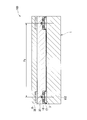
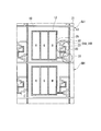
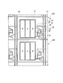
- FIG. 4 is a sectional view showing the sensor unit SU along the line BB 'shown in FIG.
- FIG. 5 is a cross-sectional view showing the sensor unit SU along the line CC ′ shown in FIG. 4 and 5 show one display unit having a width Px and a length Py.
- the display unit includes three openings 9.
- the number of openings 9 included in the capacitor pattern 12 can be, for example, a multiple of 3 or 4. Further, the number of the openings 9 may be one or more, and two openings 9 may be provided in one partition region 19 as shown in a modified example described later. Since the capacitance of the capacitor pattern 12 is proportional to the area of the capacitor pattern 12, the number of the openings 9 can be set to two or more, and further to a multiple of three or four.
- a color display in a display device is composed of three pixels of RGB (red pixel, green pixel, blue pixel) or four pixels of RGBW (red pixel, green pixel, blue pixel and further white pixel) and one display unit. Is often configured. Therefore, setting the number of openings 9 by a multiple of 3 or 4 is advantageous in relation to the display unit and the capacitor pattern 12.
- the number of the openings 9 is reduced by 1 in accordance with the necessity of reducing the parasitic capacitance between the scanning line 13 for performing touch sensing and the capacitor pattern 12 (in other words, the necessity of adjusting the distance between wirings).
- the number may be two or more or two or more.
- a color filter substrate is realized by adding a color filter of red pixel R, green pixel G, and blue pixel B to each of the plurality of openings 9. be able to.
- a protective glass cover glass
- the black matrix substrate 100 shown in FIG. 4 via the second transparent resin layer 38 (adhesive layer), and the black matrix substrate 100 may be used as a touch panel. .
- the relative permittivity of a glass or resin substrate serving as a support for supporting a transparent electrode such as ITO is often in the range of about 3 to 6.
- the electrode ECS (light-transmitting conductive film) disclosed in FIG. 2 of Patent Document 2 is in contact with a glass or resin substrate 62 as described in paragraph [0054].
- a transparent electrode such as ITO is used as a capacitor electrode (capacitor pattern) as a capacitance detecting element
- the relative permittivity of glass and resin is small, and is not a preferable material.
- ITO has a resistivity of about 2 ⁇ 10 ⁇ 4 ⁇ cm.
- copper which is a metal
- a metal such as silver, copper, aluminum, or zinc, or an alloy containing the above materials, as the material of the capacitor electrode (capacitor pattern), the scanning line, and the output line, which are the capacitance detection elements.
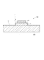
- FIG. 6 is a partially enlarged view showing the black matrix substrate 100, and is a partial cross-sectional view showing a configuration in which a black dielectric layer 3, a first insulating layer 17, and a conductive layer 7 are laminated in this order on a transparent substrate 102. is there.
- the conductive layer 7 has a three-layer structure in which the metal layer 5 is sandwiched between the conductive oxide layers 4.
- the metal layer 5 shown in FIG. 6 may be an alloy layer. As described above, the metal layer 5 and the alloy layer can be a copper layer or a copper alloy layer. The thicknesses of the two layers located above and below the conductive oxide layer 4 may be different. Note that the configuration of the conductive layer 7 can be applied to the above-described second conductive layer.
- FIG. 7 is a partially enlarged view showing the configuration of the black matrix substrate 100, and is a cross-sectional view illustrating a situation when a pointer such as a finger F contacts the first surface 1 of the black matrix substrate 100.
- a pointer such as a finger F contacts the first surface 1 of the black matrix substrate 100.
- the capacitor pattern 12 detects a change in capacitance together with the black dielectric layer 3.
- the capacitor pattern 12 sends a touch detection signal to the output line 21 via the first thin film transistor 31.
- the change in the capacitance (the amount of change in the capacitance and the change in the potential) detected by the capacitor pattern 12 is input to the first gate electrode 11 of the first thin film transistor 31.
- the scanning line 13 (the scanning line can be referred to as a power supply line) sends a selection signal to the first thin film transistor 31 provided in the sensor unit SU.
- the amount of change in capacitance input to the first gate electrode 11 is amplified by the first thin film transistor 31 and output to the output line 21.
- a control unit (not shown) connected to the output line 21 detects the touch detection signal and performs touch sensing.
- the fingerprint density of a finger is about 3 / mm.
- a touch panel with a resolution of about 10 / mm to 100 / mm can perform fingerprint authentication.
- the black matrix substrate 100 according to the present embodiment may have a resolution of 100 lines / mm or more. In the case of pen input, a resolution of several tens of microns corresponding to the pen tip is sufficient.
- the black matrix substrate 100 according to the present embodiment is applied to a smartphone, a tablet terminal, or the like corresponding to a pixel resolution exceeding 400 ppi, a touch resolution exceeding 100 lines / mm is possible.
- the width Px of the capacitor pattern 12 corresponding to these three pixels is three pixels The equivalent of 45 ⁇ m. If the unit cell width (synonymous with the unit cell pitch or the size of the display unit) of the touch sensor is 45 ⁇ m, fingerprint authentication and pen input can be sufficiently performed. Since the pitch of the unevenness of the fingerprint (ridge line and valley line of the fingerprint) is approximately 3 lines / mm, the capacitor pattern 12 only needs to have a resolution of, for example, about 10 lines / mm to 100 lines / mm. Thereby, fingerprint authentication is possible.
- the black dielectric layer 3 stores electric charges and functions as an electrostatic capacitor (capacitance) element. If the pointer is a pen tip, a change in capacitance occurs in the black dielectric layer 3 having a size close to the area of the pen tip. When the finger F presses the first surface 1 with a strong pressure, a change in capacitance occurs in the number of black dielectric layers 3 corresponding to the contact area of the finger F.
- a fingerprint pattern is two-dimensionally detected in accordance with the unevenness of the fingerprint (valley line: valley @ line, ridge line: ridge @ line).
- a distance Pz from the black dielectric layer 3 to the finger F shown in FIG. 7 may be practically in the range of about 0.1 mm to 1.5 mm.
- the distance Pz may include, for example, the thickness of a cover glass for protection and the thickness of a polarizing plate or a retardation plate. Due to the configuration of the black dielectric layer 3 having a high relative dielectric constant and the metal layer 5 (or an alloy layer) having a high electrical conductivity according to the embodiment of the present invention, the transparent substrate 102 has a thickness exceeding 0.4 mm. Even so, fingerprint authentication is possible.
- the most typical metal layer 5 (or alloy layer) material is copper and copper alloy.
- FIG. 8 is a cross-sectional view showing a black dielectric layer 3 constituting a black matrix substrate according to a modification of the first embodiment.
- FIG. 4 is a cross-sectional view illustrating a state of reflection of visible light when inserted between the body layer 3 and the body layer 3.
- the black dielectric layer is composed of two resin dispersions (black dielectric layer 3 and low-concentration carbon layer 6) having different carbon concentrations. At least one of the two layers of the resin dispersion contains a dielectric made of a metal oxide.
- the effective optical density of the low-concentration carbon layer 6 is set, for example, in the range of 0.05 to 0.4.
- the thickness of the low-concentration carbon layer 6 may be set in the range of 0.1 ⁇ m to 0.7 ⁇ m.
- the effective optical density of the black dielectric layer 3 is set, for example, in a range of 0.5 or more and less than 3.
- the thickness of the black dielectric layer 3 may be set in the range of 0.5 ⁇ m to 2 ⁇ m.
- the optical density of the black dielectric layer 3 may be set to a value exceeding 3, but setting the optical density of the black dielectric layer 3 in contact with the metal layer or the alloy layer to 3 or more has no technical meaning.
- the thickness of the low-concentration carbon layer 6 may be greater than 0.8 ⁇ m, but increasing the thickness of the low-concentration carbon layer 6 has little technical significance.
- the reflectance of visible light between the second surface 2 and the black dielectric layer 3 as viewed from the first surface 1 (viewing direction) is 0.4%. It can be: This low reflectance of 0.4% or less is a substantially flat reflectance between light wavelengths of 400 nm to 700 nm, and is different from a low reflection film of an ordinary optical multilayer. With an optical multilayer low-reflection film having a configuration in which SiO 2 / TiO 2 and the like are stacked, it is difficult to obtain a flat low reflectance in a wide wavelength range.
- the reflectance is a ratio of the reflected light 34 to the incident light 33 from the outside.
- the reflected light 34 is light that reflects the incident light 33 at the interface between the low-concentration carbon layer 6 and the second surface 2.
- the measurement of the reflectance can be performed using a microspectroscope.
- the chromaticity observed between the black dielectric layer 3 and the second surface 2 and the chromaticity observed between the low-concentration carbon layer 6 and the two layers of the black dielectric layer 3 that is, The chromaticity observed on the second surface 2 falls within a small numerical value of ⁇ 2.0 or less, and becomes a neutral color without coloring.
- the reflectance at the interface between the single layer of the black dielectric layer 3 and the second surface can be set to about 3%.
- the configuration of the black dielectric layer 3 a multilayer configuration having different electrical characteristics such as relative permittivity and resistivity can be adopted.
- electrical characteristics such as relative permittivity and resistivity can be changed in the normal direction from the pointer of the finger F or the like, that is, in the thickness direction of the black dielectric layer 3.
- the relative permittivity of the black dielectric located near the capacitor pattern 12 may be increased, and the relative permittivity of the black dielectric located far from the capacitor pattern may be decreased.
- the concentration of carbon contained in the black dielectric layer 3 may be adjusted in the thickness direction of the black dielectric layer 3. Further, the dispersion state of carbon may be changed along the thickness direction of the black dielectric layer 3.
- the black dielectric layer 3 may have a dielectric constant gradient along the thickness direction. Near the interface between the capacitor pattern 12 and the first insulating layer 17, the black dielectric layer 3 may have a partially high dielectric constant.
- a substrate having a low relative dielectric constant and a material having a relative dielectric constant of 8 or less can be used as the transparent substrate 102.
- the relative permittivity of the transparent substrate 102 may be, for example, 5 or less.
- the reset for example, ground
- the reset period can be shortened by setting the resistivity of the black dielectric layer 3 to 10 8 ⁇ cm or more and less than 10 13 ⁇ cm.
- FIG. 9 is a circuit diagram illustrating a sensor unit included in a black matrix substrate according to Modification 2 of the first embodiment.
- the black matrix substrate according to the second modification includes a sensor unit SU1.
- the sensor unit SU1 includes a reset transistor 32 (second thin film transistor) in addition to the configuration of the sensor unit SU including the first thin film transistor 31 illustrated in FIG.
- the reset transistor 32 includes a second gate electrode 27 electrically connected to the first gate electrode 11, a second source electrode 25, and a second drain electrode 26 electrically connected to the second gate electrode 27 (short-circuited to the second gate electrode 27).
- Part of the first conductive pattern 10 forms the second gate electrode 27.
- Part of the second conductive pattern 20 forms a second source electrode 25 and a second drain electrode 26.
- Part of the oxide semiconductor layer forms the second channel layer 24A.
- Part of the second insulating layer 48 constitutes the gate insulating layer 24B of the second thin film transistor.
- the second channel layer 24A is formed at the same time when the first channel layer 16 is formed.
- the gate insulating layer 24B is formed simultaneously with the formation of the second insulating layer 48.
- the scanning line 13 not only supplies a scanning signal to the first source electrode 22 of the first thin film transistor 31, but also supplies a reset signal (for example, a ground potential) to the reset transistor 32.
- a reset signal for example, a ground potential
- the supply of such a scanning signal and the supply of a reset signal are performed by time division.
- the reset transistor 32 receives a reset signal from the scanning line 13 and resets the potential of the capacitor pattern 12.
- FIG. 10 is a circuit diagram illustrating a sensor unit included in a black matrix substrate according to Modification 3 of the first embodiment. 10, the same members as those of the sensor unit SU1 shown in FIG. 9 are denoted by the same reference numerals, and the description thereof will be omitted or simplified.
- the black matrix substrate according to the third modification includes a sensor unit SU2.
- the sensor unit SU2 includes, in addition to the configuration of the sensor unit SU including the first thin film transistor 31 shown in FIG. 1, a reset transistor 32 shown in FIG. 9 and a source extension 28 extending the second source electrode 25 of the reset transistor 32. And a reset line 15.
- the reset line 15 supplies a reset signal to the reset transistor 32 via the second source electrode 25 and the source extension 28.
- the source extension 28 is not connected to the scanning line 13, but is connected to the reset line 15 via the contact hole 29.
- the sensor unit SU2 can receive the reset signal from the reset line 15 independently of the scan signal from the scan line 13. In the sensor unit SU2, it is not necessary to supply the scanning signal and the reset signal as shown in FIG. As in the case of the sensor unit SU shown in FIG.
- FIG. 1 is a circuit diagram in which one sensor unit includes one thin film transistor.
- 9 and 10 are circuit diagrams in which one sensor unit includes two thin film transistors. However, the number of thin film transistors in one sensor unit can be increased as needed.
- FIG. 11 is a partially enlarged view showing a black matrix substrate according to Modification 4 of the first embodiment, and shows the arrangement of the first conductive pattern 10 and the second conductive pattern 20 provided on the black dielectric layer 3.
- FIG. FIG. 11 shows a modification of the capacitor pattern 12 shown in FIG. 3, and shows a case where two openings 9 are formed in the partition region 19.
- the line widths of the conductive lines B1, B2, and B3 forming a part of the capacitor pattern 12 may be different from each other.
- FIG. 12 is a view showing a display device according to the second embodiment of the present invention, and is a cross-sectional view partially showing a micro LED display device 200 to which the black matrix substrate 100 according to the first embodiment is applied. .
- the second surface 2 of the black matrix substrate 100 faces the second array substrate 201.
- the light emitting elements CHIP are arranged on the surface of the second array substrate 201 facing the second surface 2.
- the black matrix substrate 100 and the second array substrate 201 are bonded via an adhesive layer 108 made of a transparent resin.
- the sensor unit SU (unit cell, see FIG. 1) of the black matrix substrate 100 includes the capacitor pattern 12 and the first thin film transistor 31, and employs the individual reading method.
- the technique using such an individual reading method is a technique close to the self-capacitance method.
- Patent Literature 3 and Patent Literature 4 exemplified as the prior art of the display device each use a mutual capacitance method using X-direction wiring and Y-direction wiring, and the capacitance by touch sensing is used. Is greatly different from the second embodiment.
- the capacitive element CS1 having a capacitance includes an electrode ECS, which is a light-transmitting conductive film, an electrode COM, and an insulating layer.
- Patent Document 2 does not disclose a configuration in which a black dielectric is laminated on a copper wiring.
- FIG. 13 is an enlarged view partially showing the second array substrate 201 included in the micro LED display device 200 according to the second embodiment, and is a cross-sectional view partially showing the third thin film transistor 68.
- FIG. 14 is a cross-sectional view showing a light-emitting element (micro LED) mounted on the micro LED display device 200 according to the second embodiment, and is an enlarged view partially showing a region indicated by reference numeral C in FIG.
- FIG. 15 is an enlarged cross-sectional view illustrating the micro LED display device 200 according to the second embodiment, in which the third source electrode 54 stacked on the third channel layer 58 of the third thin film transistor 68 illustrated in FIG.
- FIG. 3 is a diagram illustrating a laminated structure of a three drain electrode 56.
- the material forming the second substrate 202 of the second array substrate 201 does not need to be limited to a transparent substrate.
- a substrate applicable to the second substrate 202 a glass substrate, a ceramic substrate, a quartz substrate, a sapphire substrate, a semiconductor substrate of silicon, silicon carbide, silicon germanium, or the like, a plastic substrate, or the like can be given.
- the second substrate 202 may be a transparent substrate, an opaque substrate, or a colored substrate.
- 4A fourth insulating layer 47 is formed on the surface 43 of the second substrate 202.
- the third thin film transistor 68, the third insulating layer 148 formed so as to cover the fourth insulating layer 47 and the third thin film transistor 68, and the third channel layer 58 of the third thin film transistor 68 are opposed.
- the first flattening layers 96 formed as described above are sequentially stacked.
- a contact hole 93 is formed in the first planarization layer 96, the sixth insulating layer 49, and the third insulating layer 148 at a position corresponding to the third drain electrode 56 of the third thin film transistor 68.
- a bank 94 (see FIG. 13) is formed on the first planarization layer 96 at a position corresponding to the third channel layer 58.
- the upper surface of the first planarization layer 96, the inside of the contact hole 93, and the third drain electrode A reflection electrode 89 (pixel electrode) is formed so as to cover 56.
- the reflection electrode 89 may not be formed on the upper surface of the bank 94.
- the reflection electrode 89 is electrically connected to the lower electrode 88 of the light emitting element CHIP via the conductive bonding layer 77.
- a second planarization layer 95 is formed so as to fill the inside of the contact hole 93 and to cover the reflective electrode 89 and the light emitting element CHIP.
- a transparent conductive film 76 called ITO is formed, and the transparent conductive film 76 (synonymous with the second power supply line 52) has an upper electrode 87 constituting the light emitting element CHIP. Is connected.
- an auxiliary conductor 75 is formed on the transparent conductive film 76, and the transparent conductive film 76 is electrically connected to the auxiliary conductor 75.
- a sealing layer 109 is formed on the surface of the transparent conductive film 76 so as to cover the auxiliary conductor 75.
- the auxiliary conductor 75 is a conductor for reducing the resistance value of the transparent conductive film 76 in plan view.
- an organic resin such as an acrylic resin, a polyimide resin, and a novolak phenol resin can be used.
- an inorganic material such as silicon oxide or silicon oxynitride may be further laminated.
- an acrylic resin, a polyimide resin, a benzocyclobutene resin, a polyamide resin, or the like may be used as a material of the first flattening layer 96 and the second flattening layer 95.
- a low dielectric constant material (low-k material) can also be used as a material of the first flattening layer 96 and the second flattening layer 95.
- any one of the first planarization layer 96, the second planarization layer 95, and the sealing layer 109 may have a light scattering function in order to improve visibility.
- the reflection electrode 89 is in contact with the third drain electrode 56 (fourth wiring).
- the reflective electrode 89 has a conductive metal oxide layer as an upper layer, and the third drain electrode 56 is in contact with the conductive metal oxide layer.
- the reflective electrode 89 has a three-layer structure in which a silver alloy is sandwiched between conductive metal oxide layers.
- Each of the conductive metal oxide layer of the reflective electrode 89 and the conductive metal oxide layer of the third drain electrode 56 is formed of a conductive metal oxide, and can make ohmic contact.
- the surface in contact with the reflective electrode 89 in the contact hole 93 is an oxidized copper surface or aluminum, it is difficult to obtain an ohmic contact.
- Aluminum has insufficient physical adhesion to a conductive metal oxide such as ITO.
- the configuration employed in the micro LED display device 200 according to the second embodiment can provide a wiring structure capable of making ohmic contact in this manner.
- the light emitting element CHIP is a vertical light emitting diode that functions as a display function layer, and is provided for each of a plurality of pixels located on the second substrate 202.
- the light-emitting element CHIP has a structure in which an upper electrode 87, an n-type semiconductor layer 90, a light-emitting layer 92, a p-type semiconductor layer 91, and a lower electrode 88 are stacked in this order.
- the light emitting element CHIP has a configuration in which the p-type semiconductor layer 91, the light-emitting layer 92, the n-type semiconductor layer 90, and the upper electrode 87 are stacked on the lower electrode 88 in this order.
- electrodes used for LED light emission are formed on different surfaces, and are formed on surfaces facing each other.
- an upper electrode 87 and a lower electrode 88 are arranged outside the surfaces facing the n-type semiconductor layer 90 and the p-type semiconductor layer 91 which are stacked so as to be parallel to each other.
- the light emitting element CHIP having such a structure is referred to as a vertical light emitting diode. If the LED structure has a different shape such as a pyramid shape in cross-sectional view, it is not included in the vertical light emitting diode of the present invention.
- a structure in which electrodes are arranged on one surface or a structure in which electrodes are arranged in a horizontal direction is called a horizontal light emitting diode.
- the transparent conductive film 76 overlaps the upper electrode 87 and is electrically connected.
- the corner 74 of the light emitting element CHIP is covered with the second planarization layer 95.
- an overlapping portion 71 where the second planarization layer 95 and the upper electrode 87 overlap is formed. Since the overlapping portions 71 are formed at both ends of the upper electrode 87, the second flattening layer 95 has a concave shape on the upper electrode 87.
- the second planarization layer 95 formed on the upper electrode 87 has a taper with an angle ⁇ in order to reduce the risk of disconnection of the transparent conductive film 76.
- a transparent conductive film 76 is formed along the tapered surface of the second planarization layer 95.
- the overlapping portion 71 is located between the transparent conductive film 76 and the upper electrode 87 at the corner portion 74 and is inclined with respect to the surface of the upper electrode 87 at an angle ⁇ of, for example, 5 ° to 70 °. are doing. Since the overlapping portion 71 has such an inclination, disconnection of the transparent conductive film 76 can be prevented.
- the transparent conductive film 76 is formed. Is liable to be disconnected, and there is a concern that lighting failure of the light emitting element CHIP may occur.
- known photolithography As a method of forming the second planarization layer 95 having the above-described concave shape and a method of forming the overlapping portion 71 overlapping the light emitting element CHIP, known photolithography is employed. Further, a dry etching technique may be applied in addition to a known photolithography technique.
- the shape of the light emitting element CHIP for example, a square shape having a side length of 3 ⁇ m to 500 ⁇ m in plan view can be applied. However, shapes other than squares and rectangles may be applied. Alternatively, the size of one side may be 500 ⁇ m or more.
- one or two or more light-emitting elements can be mounted on a pixel partitioned by the third gate wiring 69 and the third source wiring 66 (see FIG. 16).
- the direction of the square light emitting element CHIP can be randomly rotated in units of 90 degrees. By performing random mounting, it is possible to reduce color unevenness and brightness unevenness of the entire screen caused by slight variations in LED crystal growth.
- a constituent material of the lower electrode 88 silver, a silver alloy, aluminum, or an aluminum alloy can be used. Further, as a configuration of the lower electrode 88, a configuration in which a silver or silver alloy layer is sandwiched between conductive metal oxide layers may be applied, as described later. Part of the configuration of the lower electrode 88 includes a metal layer such as a Ti layer, a Cr layer, a Pt layer, an AuGe layer, a Pd layer, a Ni layer, a TiW layer, a Mo layer, and the above-described conductive metal oxide layer. A multilayer configuration may be introduced. Note that a transflective or transmissive display device can be realized by reducing the area ratio of the lower electrode 88 in a plan view.
- the upper electrode 87 preferably has a configuration including a layer formed of a conductive metal oxide.
- a conductive metal oxide it is preferable that at least the surface layer of the upper electrode 87 is formed of a conductive metal oxide.
- the conductive metal oxide forming the surface layer of the upper electrode 87 be electrically connected to the conductive layer formed of the conductive metal oxide.
- the bonding layer 77 can be formed of, for example, a conductive material capable of fusing the lower electrode 88 and the reflective electrode 89 of the light emitting element CHIP within a temperature range of 150 ° C. to 340 ° C. and making an electrical connection.
- a conductive aggregate such as silver, carbon, and graphite may be dispersed in the heat-flowable resin.
- the bonding layer 77 may be made of In (indium), InBi alloy, InSb alloy, InSn alloy, InAg alloy, InGa alloy, SnBi alloy, SnSb alloy, or the like, or a ternary or quaternary low-melting metal. Can be formed.
- the lower electrode 88 and the reflective electrode 89 are self-aligned. Can be fused.
- various energies such as heat, pressurization, electromagnetic waves, laser light, and a combination of these and ultrasonic waves are used. It should be noted that the vertical light emitting diode has an advantage that repair can be easily performed when a bonding failure occurs.
- the position of the light emitting diode is reduced by reducing the contact angle (wetting property) between the lower electrode 88 and the reflective electrode 89 and the bonding layer 77 to be melted by heating. Matching is possible.
- a horizontal type light emitting diode in which electrodes are arranged in the same direction at the lower part, there are disadvantages that it is difficult to perform a junction inspection of individual diodes and that electrodes are easily short-circuited at the time of repair (replacement of a defective diode or the like). From this viewpoint, a vertical light emitting diode is preferably used.
- the bonding layer 77 can be patterned by a well-known photolithography method or lift-off means.
- FIGS. 13 and 15 show an example of the structure of a thin film transistor (TFT) having a top gate structure used as the third thin film transistor 68 connected to the reflective electrode 89 (pixel electrode).
- the structure of the third thin film transistor 68 is also applied to a fourth thin film transistor 67 described later.
- the third thin film transistor 68 has a configuration in which a third source electrode 54 and a third drain electrode 56 are stacked on a third channel layer 58.
- the third thin film transistor 68 includes a third drain electrode 56 connected to one end of the third channel layer 58 (the left end of the third channel layer 58 in FIG. 15) and the other end of the third channel layer 58 (see FIG. 15, a third source electrode 54 connected to the third channel layer 58 (right end of the third channel layer 58), and a third gate electrode 55 disposed opposite to the third channel layer 58 via the gate insulating layer (third insulating layer 148).
- Third gate electrode 55 has the same configuration as conductive layer 7 shown in FIG. That is, the third gate electrode 55 has a three-layer structure in which the metal layer 5 (alloy layer) is sandwiched between the conductive oxide layers 4.
- the overlapping portion 161 which is an interface where the third channel layer 58 contacts the third source electrode 54 and the interface where the third channel layer 58 contacts the third drain electrode 56 are formed.
- a certain overlapping portion 162 is formed.
- the contact resistance at the interface between the third channel layer 58 and the conductive oxide layer 4 is small, and an ohmic contact can be obtained.
- the conductivity of the conductive oxide layer 4 is high, a conductive metal oxide having substantially high mobility is formed on the third channel layer 58. As a result, transistor characteristics can be improved.
- the conductive oxide layer 4 serves as a high mobility semiconductor layer of the third channel layer 58.
- the third channel layer 58 is made of an oxide semiconductor and is in contact with the third insulating layer 148 which is a gate insulating layer.
- the third thin film transistor 68 drives the light emitting element CHIP.
- the figure does not have a tapered surface.
- a tapered surface inclined surface is formed on an electrode or a channel layer constituting the third thin film transistor 68.
- FIG. 13 shows a structure in which the third channel layer 58, the third source electrode 54, and the third drain electrode 56 of the third thin film transistor 68 are formed on the fourth insulating layer 47. Does not limit such a structure.
- the third thin film transistor 68 may be formed directly on the second substrate 202 without providing the fourth insulating layer 47. Further, a thin film transistor having a bottom gate structure may be applied.
- the third source electrode 54 and the third drain electrode 56 shown in FIG. 13 are formed simultaneously in the same step.
- the third source electrode 54 and the third drain electrode 56 include conductive layers having the same configuration. That is, in the second embodiment, each of the third source electrode 54 and the third drain electrode 56 has a three-layer structure in which a copper or copper alloy layer is sandwiched between conductive oxide layers.
- the third source electrode 54 and the third drain electrode 56 may have a three-layer structure of titanium / aluminum alloy / titanium, molybdenum / aluminum alloy / molybdenum, or the like.
- the aluminum alloy is a typical alloy of aluminum-neodymium.
- a back gate electrode may be provided to stabilize the threshold voltage (Vth) of the third thin film transistor 68 or to obtain stable normally-off transistor characteristics.
- the back gate electrode is formed by patterning a metal film on the opposite side of the third channel layer 58, for example, on the interface between the fourth insulating layer 47 and the second substrate 202 so as to face the third gate electrode 55 shown in FIG. Thus, a back gate electrode can be formed.
- the back gate electrode By forming the back gate electrode with a metal film, the incidence of external light toward the third channel layer 58 can be prevented, and a stable “positive (plus)” Vth can be obtained. Note that a negative voltage is usually applied to the back gate electrode.
- the third channel layer 58 can be electrically surrounded by an electric field formed between the third gate electrode 55 and the back gate electrode.
- the drain current of the third thin film transistor 68 can be increased, and the leak current, which is the off current of the third thin film transistor 68, can be further reduced. Therefore, the relative size of the third thin film transistor 68 can be reduced with respect to the drain current required for the third thin film transistor 68, and the degree of integration as a semiconductor circuit can be improved.
- a thin film transistor including a channel layer formed using an oxide semiconductor has extremely low leakage current, and thus has high stability after input of a scanning signal or a video signal.
- a thin film transistor including a channel layer formed using a polysilicon semiconductor has a larger leakage current by two digits or more than a transistor including an oxide semiconductor. It is preferable that the leakage current is small because it contributes to high-accuracy touch sensing.
- IG IGZO indium oxide, zinc oxide, and gallium oxide
- An oxide semiconductor called IGZO is formed collectively by vacuum film formation such as sputtering. After the oxide semiconductor is formed, heat treatment after pattern formation of a TFT or the like is also performed at one time. For this reason, variations in electrical characteristics (for example, Vth) related to the channel layer are extremely small. In driving the LED, it is necessary to suppress the variation in Vth of the thin film transistor to a small range in order to suppress the variation in brightness.
- an oxide semiconductor called IGZO is often subjected to heat treatment in a temperature range of 400 ° C. to 700 ° C. (high-temperature annealing) in order to secure reliability by crystallization. In the manufacturing process of a liquid crystal display device or the like, during this heat treatment, copper diffusion often occurs, and the conductivity of the copper wiring often deteriorates significantly.
- Annealing above 350 ° C. may increase the diffusion of copper and possibly degrade the properties of the oxide semiconductor.
- a heat treatment exceeding 400 ° C. may cause interdiffusion between copper and titanium or the like, and may deteriorate the electrical resistivity of the copper wiring.
- cerium oxide can be included in the oxide semiconductor.
- the oxide semiconductor is a composite oxide containing indium oxide, antimony oxide, and cerium oxide having a smaller amount than each of indium oxide and antimony oxide, and counts oxygen.
- the amounts of indium and antimony are 40 at% or more.
- the amounts of indium and antimony are 48 at%, and the amount of cerium is 4 at%.
- antimony oxide and cerium oxide unlike gallium oxide and indium oxide, can be obtained at a low price and thus have high industrial value.
- the concentration of indium oxide or the concentration of cerium oxide may be changed in the thickness direction of the third channel layer 58.
- the third channel layer 58 may be formed using a plurality of layers having different concentrations of cerium oxide.
- the acid resistance of the third channel layer 58 can be increased by making the composition of the surface layer of the third channel layer 58 rich in cerium oxide in order to enhance wet etching processability of the source electrode and the like.
- An etching stopper layer may be stacked on the third channel layer 58.
- the composite oxide thin film containing cerium oxide becomes a film having high acid resistance by annealing at 180 ° C. or higher, the etching stopper layer is actively used. Insertion is unnecessary, and the etching stopper layer forming step can be omitted.
- This acid resistance can also be obtained by increasing the concentration of cerium oxide in the composite oxide film.
- the oxide semiconductor layer contains tin oxide.
- increasing the concentration of tin oxide improves the acid resistance of the composite oxide.
- annealing at 180 ° C. or higher can further improve acid resistance. Even when both cerium oxide and tin oxide are added to the composite oxide containing indium oxide as a main material, the acid resistance can be similarly improved and the etching stopper layer can be eliminated.
- the annealing temperature may be in the range of 180 ° C. to 340 ° C., and a temperature higher than 200 ° C. is more preferable.
- pre-annealing at, for example, about 220 ° C. before forming a pattern such as a source electrode, the resistance of the oxide semiconductor layer (composite oxide film) to an etchant can be improved.
- This pre-annealing may be performed before forming a conductive layer for forming a source electrode.
- FIG. 16 is a typical circuit diagram including a thin film transistor for driving a micro LED.
- the light emitting element CHIP is illustrated as the light emitting diode element.
- the plurality of pixels PX are arranged in a matrix.
- the pixel PX may be referred to as a pixel opening PX.
- the circuit diagram shown in FIG. 16 is also applicable to an organic EL display device 300 according to a third embodiment described later. In this case, an organic EL layer is used as a light emitting diode element.
- FIG. 16 schematically illustrates a plurality of pixels PX.
- Each pixel PX includes a source line 66 (third source line) serving as a video signal line and a gate line 69 (third source line) serving as a scanning line. (Gate wiring).
- the third thin film transistor 68 is connected to the first power supply line 51 via the third source electrode 54.
- the first power supply line 51 is a power supply line that supplies power to the light emitting element 86 (the light emitting element CHIP).
- the second power supply line 52 is connected through a transparent conductive film 76 and an auxiliary conductor 75 to an upper electrode 87 constituting the light emitting element 86.
- the second power supply line 52 is maintained at a constant potential, and may be grounded to, for example, a ground (a casing or the like).
- auxiliary conductor 75 a metal wiring having good conductivity can be used, and can be formed at a position avoiding the pixel opening (pixel PX).
- auxiliary conductor 75 has a stacked structure of a conductive metal oxide, a copper alloy, and a conductive metal oxide.
- a third thin film transistor 68, a fourth thin film transistor 67, a light emitting element 86, a capacitor 79, and the like are arranged in a pixel PX (pixel opening) defined by a source wiring 66 and a gate wiring 69. Have been.
- the fourth thin film transistor 67 is electrically linked to the source wiring 66 and the gate wiring 69.
- the third thin film transistor 68 is electrically linked with the fourth thin film transistor 67 and the first power supply line 51.
- the third thin film transistor 68 receives a signal from the fourth thin film transistor 67 and drives a light emitting element 86 which is a vertical light emitting diode.
- the third gate electrode 55 of the third thin film transistor 68 is connected to the first power supply line 51 via the capacitor 79.
- the third thin film transistor 68 and the fourth thin film transistor 67 constitute a thin film transistor array.
- FIG. 16 shows main electrical elements including the first power supply line 51 and disposed on the front surface 43 of the second substrate 202.
- the plurality of pixels PX arranged in a matrix form an effective display area of the display device.
- a thin film transistor or the like for performing a capacitance reset process may be separately provided as a switching element.
- the switching element that performs the reset process is connected to a reset signal line formed on the front surface 43 of the second substrate 202.
- the gate wiring 69 is connected to a scan driving circuit 82 (gate signal switching circuit) including a shift register.
- the source wiring 66 is connected to a source signal circuit 81 (source signal switching circuit) including a shift register, a video line, and an analog switch.
- the source signal circuit 81 and the scan driving circuit 82 control a light emitting element 86 which is a display function layer in response to a signal from the display control unit.
- the first power supply line 51 and the source wiring 66 extend in the Y direction (second direction).
- the gate wiring 69 extends in the X direction (first direction).
- the positional relationship between the source wiring 66, the gate wiring 69, the first power supply line 51, and the second power supply line 52 is not limited.
- the direction of the pattern of the transparent conductive film 76 can be changed depending on the number of thin film transistors or the direction of the auxiliary conductor 75 in one pixel PX.
- a signal (drain) from the fourth thin film transistor 67 functioning as a switching transistor is output to the third gate electrode 55. That is, an ON signal is input to the third gate electrode 55 of the third thin film transistor 68 that supplies power to the pixel PX.
- the third thin film transistor 68 functioning as a driving transistor receives a signal from the third gate electrode 55 and supplies power to the light emitting element 86 from the first power supply line 51.
- a current is supplied from the first power supply line 51 to the light emitting element 86 via the third channel layer 58 of the third thin film transistor 68, and the pixel PX (the light emitting element 86) emits light according to the amount of the current.
- FIG. 17 is a view showing a display device according to the third embodiment of the present invention, and is a cross-sectional view partially showing an organic EL display device 300 to which a third black matrix substrate 303 is applied.
- FIG. 18 is a partial cross-sectional view of a third array substrate 301 on which an organic EL layer is mounted in the organic EL display device 300 according to the third embodiment.
- a third black matrix substrate 303 and a third array substrate 301 having the organic EL layer 80 are bonded to face each other.
- the third black matrix substrate 303 includes a color filter including red pixels R, green pixels G, and blue pixels B.
- the red pixel R, the green pixel G, and the blue pixel B are provided in the opening of the light absorption layer 8.
- Other configurations of the third black matrix substrate 303 are the same as those of the black matrix substrate 100 described in the first embodiment.
- the organic EL layer 80 including the light emitting layer 92 will be described later in detail.
- the third substrate 302 of the third array substrate 301 does not need to be limited to a transparent substrate.
- applicable substrates include a glass substrate, a ceramic substrate, a quartz substrate, a sapphire substrate, silicon, silicon carbide, and silicon germanium. Semiconductor substrate or a plastic substrate.
- a fourth insulating layer 47 is formed on the third substrate 302 of the third array substrate 301.
- the fifth thin film transistor 70, the fifth insulating layer 248 formed so as to cover the fourth insulating layer 47 and the fifth thin film transistor 70, and the third channel layer 58 of the fifth thin film transistor 70 are opposed.
- the formed first planarization layers 96 are sequentially stacked.
- a contact hole 93 is formed in the first planarization layer 96, the sixth insulation layer 49, and the fifth insulation layer 248 at a position corresponding to the fifth drain electrode 156 of the fifth thin film transistor 70.
- a bank 94 is formed on the first planarization layer 96 at a position corresponding to the third channel layer 58. In a region between the banks 94 adjacent to each other in a sectional view, that is, in a region surrounded by the banks 94 in a plan view, the upper surface of the first planarization layer 96, the inside of the contact hole 93, and the fifth drain electrode A lower electrode 189 (pixel electrode) is formed so as to cover 156. Note that the lower electrode 189 may not be formed on the upper surface of the bank 94.
- a hole injection layer 191 is formed so as to cover the lower electrode 189, the bank 94, and the first planarization layer 96.
- the light emitting layer 92, the upper electrode 87, and the sealing layer 195 are sequentially stacked on the hole injection layer 191.
- the lower electrode 189 has a configuration in which a silver or silver alloy layer is sandwiched between conductive oxide layers, as described later.
- the upper electrode 87 is, for example, a transparent conductive film in which a silver alloy layer having a thickness of 11 nm is sandwiched between composite oxides having a thickness of 40 nm.
- the lower electrode 88 has a configuration in which a silver alloy layer having a thickness of 250 nm is sandwiched between composite oxides having a thickness of 30 nm. Note that the composite oxide layer is applied to a conductive metal oxide layer, the thickness of the silver alloy layer is set to, for example, 9 nm to 15 nm, and the silver alloy layer is sandwiched between the conductive metal oxide layers. It is preferable to use a three-layer laminated structure. In this case, a transparent conductive film having a high transmittance can be realized.
- the composite oxide layer is applied to a conductive metal oxide layer, and the thickness of the silver alloy layer is set, for example, in the range of 100 nm to 250 nm, or 300 nm or more.
- a three-layer structure in which a silver alloy layer is sandwiched between material layers may be employed. In this case, a reflective electrode having high reflectance with respect to visible light can be realized.
- an organic resin such as an acrylic resin, a polyimide resin, and a novolak phenol resin can be used.
- an inorganic material such as silicon oxide or silicon oxynitride may be further laminated.
- an acrylic resin, a polyimide resin, a benzocyclobutene resin, a polyamide resin, or the like may be used.
- a low dielectric constant material (low-k material) can also be used.
- any of the first planarization layer 96, the sealing layer 109, and the third substrate 302 may have a light scattering function in order to improve visibility.
- a light scattering layer may be formed above the third substrate 302.
- the structure of the fifth thin film transistor is the same as that of the second embodiment, and a description thereof will be omitted.
- FIG. 19 is a diagram illustrating a display device according to a fourth embodiment of the present invention, and is a cross-sectional view partially illustrating a liquid crystal display device 400 to which a fourth black matrix substrate 403 is applied.
- FIG. 20 is a typical circuit diagram including a thin film transistor for driving a liquid crystal layer applied to the display device according to the fourth embodiment.
- FIG. 21 is a cross-sectional view partially showing a liquid crystal display device employing a conventional horizontal alignment liquid crystal (FFS mode), and shows an equipotential when a liquid crystal driving voltage is applied between a pixel electrode and a common electrode. It is sectional drawing explaining the situation of a line.
- FIG. 10 horizontal alignment liquid crystal
- FIG. 22 is a cross-sectional view partially showing a liquid crystal display device employing a conventional horizontal alignment liquid crystal (FFS mode), and shows an equipotential when a transparent electrode is provided on a transparent resin layer of an opposing substrate. It is sectional drawing explaining the situation of a line.
- FFS mode horizontal alignment liquid crystal
- the liquid crystal display device 400 has a configuration in which the second surface 2 of the fourth black matrix substrate 403 on which the sensor units SU are formed and the fourth array substrate 401 are bonded via the liquid crystal layer 60.
- FIG. 19 illustration of an optical film including a polarizing plate, an alignment film, a backlight unit, and the like are omitted.
- an active element such as a thin film transistor is well known, so that the illustration of the thin film transistor is omitted.
- the fourth black matrix substrate 403 has the same configuration as the third black matrix substrate 303 of the third embodiment.
- a color filter of a red pixel R, a green pixel G, and a blue pixel B is provided in each of the openings of the light absorption layer 8.
- the liquid crystal layer 60 uses a horizontally aligned liquid crystal called an FFS method.
- FFS horizontally aligned liquid crystal
- the present embodiment is not limited to horizontal alignment or FFS driving.
- Vertically aligned liquid crystal may be employed, and the liquid crystal may be driven by a vertical electric field (a driving voltage applied in the thickness direction of the liquid crystal layer).
- the pixel electrode and the common electrode for driving the liquid crystal layer 60 are both formed by patterning a transparent conductive film into an electrode shape.
- the sixth thin film transistor 171 is driven by a gate wiring 164 extending from the scanning signal circuit 72 and a source wiring 165 extending from the video signal circuit 73.
- Patent Documents 2 and 3 described above disclose liquid crystal display devices that use a transparent conductive oxide or a light-transmitting conductive film (hereinafter, referred to as a transparent electrode) as a touch sensor.
- a transparent electrode a transparent conductive oxide or a light-transmitting conductive film
- a liquid crystal layer is driven by an array substrate arranged so as to face the touch sensor.
- the transparent electrode used for the touch sensor has a structure substantially in contact with the liquid crystal layer.
- an FFS type liquid crystal display device 700 as shown in FIG. 21 As a general configuration, an FFS type liquid crystal display device 700 as shown in FIG. 21 is known.
- the liquid crystal display device 700 has a structure in which a liquid crystal layer 607 is sandwiched between an array substrate 605 and a color filter substrate 500.
- the array substrate 605 includes an insulating layer 604 formed over the substrate 606, a common electrode 602 formed over the insulating layer 604, an insulating layer 603 formed over the common electrode 602, and a pixel formed over the insulating layer 603.
- An electrode 601 is provided.
- a color filter CF and a transparent resin layer 614 formed of a material (electrically non-conductive) through which electricity does not flow are laminated on the transparent substrate 501.
- illustration of the alignment film is omitted.
- the liquid crystal layer 607 is driven by a voltage applied between the pixel electrode 601 and the common electrode 602.
- equipotential lines 609 indicating an electric field generated from the pixel electrode 601 extend from the pixel electrode 601 toward the color filter CF so as to penetrate the liquid crystal layer 607, and
- the oriented liquid crystal rotates horizontally around the equipotential line 609, and the liquid crystal display device 700 performs standard display.
- a liquid crystal display device 800 including a color filter substrate 500 having a transparent electrode 612 so as to cover a transparent resin layer 614 is also known as an FFS type liquid crystal display device.
- the transparent electrode 612 is used as a drive electrode or a detection electrode for touch sensing.
- a liquid crystal layer 607 is disposed between the transparent electrode 612 and the pixel electrode 601. Note that the liquid crystal display device 800 is different from the liquid crystal display device 700 in that the transparent electrode 612 is formed on the color filter substrate 500.
- Other configurations of the liquid crystal display device 800 are the same as those of the liquid crystal display device 700.
- the liquid crystal molecules in the horizontal alignment may rise toward the pointer.
- the liquid crystal molecules have different dielectric constants in the major axis direction (rise direction) and the minor axis direction of the molecules, and the capacitance of the display pixel changes. Therefore, when a transparent electrode having a size including a display pixel is used as a capacitive element (drive electrode or detection electrode) for touch sensing, the capacitance variation of the display pixel becomes the capacitance variation (noise) of the touch.
- the techniques disclosed in Patent Literature 2 and Patent Literature 3 involve such a risk of noise generation. Therefore, the touch sensors disclosed in Patent Literature 2 and Patent Literature 3 have the above-described problem when applied to an FFS type liquid crystal display device.
- the fourth black matrix substrate 403 according to the fourth embodiment a structure in which a transparent electrode corresponding to the size of a pixel is not provided in the opening 9 is possible. Therefore, the liquid crystal molecules do not rise toward the transparent electrode as described above. Further, there is no change in the capacitance of the display pixel, which may be a problem in Patent Documents 2 and 3.
- the fourth black matrix substrate 403 according to the fourth embodiment is applicable not only to the FFS type liquid crystal display device but also to other display devices. Furthermore, also in the above-mentioned embodiment, a transparent electrode is not used as a touch capacitive element.
- the FFS A liquid crystal display with a high transmittance can be performed without a large adverse effect on the transmittance of the liquid crystal layer 60 driven by the method.
- the black matrix substrate according to the above-described embodiment, or the display device including the black matrix substrate, can be applied to various applications.
- the electronic devices to which the display device according to the above-described embodiments can be applied include a mobile phone, a portable game device, a personal digital assistant, a personal computer, an electronic book, a video camera, a digital still camera, a head-mounted display, a navigation system, and a sound system.
- Electronic devices such as playback devices (car audio, digital audio players, etc.), copiers, facsimile machines, printers, multifunction printers, vending machines, automatic teller machines (ATMs), personal authentication devices, optical communication devices, IC cards, etc. And the like.
- the above embodiments can be freely combined and used.
- Potential line 612 transparent electrode, 614 transparent resin layer, B blue pixel, B1, B2, B3 conductive line, CF color filter, F finger, G green pixel, OP opening (second opening), PX pixel (pixel opening ), R ⁇ red pixel, SU, SU1, SU2 ⁇ sensor unit.
Landscapes
- Physics & Mathematics (AREA)
- Engineering & Computer Science (AREA)
- Nonlinear Science (AREA)
- General Physics & Mathematics (AREA)
- Optics & Photonics (AREA)
- Mathematical Physics (AREA)
- Chemical & Material Sciences (AREA)
- Crystallography & Structural Chemistry (AREA)
- Theoretical Computer Science (AREA)
- Microelectronics & Electronic Packaging (AREA)
- General Engineering & Computer Science (AREA)
- Human Computer Interaction (AREA)
- Thin Film Transistor (AREA)
- Liquid Crystal (AREA)
- Devices For Indicating Variable Information By Combining Individual Elements (AREA)
Abstract
Description
本発明は、タッチセンシング機能を具備したブラックマトリクス基板、及び、このブラックマトリクス基板を用いた表示装置に関する。 The present invention relates to a black matrix substrate having a touch sensing function and a display device using the black matrix substrate.
静電容量方式によるタッチセンシング機能を備えたスマートフォンやタブレット端末等、指やポインタで、直接、表示画面に入力できる表示装置が一般的になりつつある。タッチセンシング機能として、液晶、マイクロLED(微小なLEDチップがマトリクス状に配列したLEDディスプレイ)、有機EL(有機エレクトロルミネセンス)等のディスプレイ表面にタッチパネルを貼り付けたオンセル方式や、液晶や有機ELの表示装置の内側にタッチセンシング機能を持たせたインセル方式が知られている。近年では、オンセル方式からインセル方式に移行しつつある。 2. Description of the Related Art Display devices that can directly input a display screen with a finger or a pointer, such as a smartphone or a tablet terminal having a touch sensing function using a capacitance method, are becoming common. Touch-sensing functions include an on-cell method in which a touch panel is attached to a display surface such as a liquid crystal, micro LED (LED display in which minute LED chips are arranged in a matrix), organic EL (organic electroluminescence), and liquid crystal and organic EL. There is known an in-cell system in which a touch sensing function is provided inside a display device. In recent years, there has been a shift from an on-cell system to an in-cell system.
指やペン等のポインタによるタッチセンシングにおいては、携帯端末機器等における一般的なタッチセンシングの他に、指紋の凹凸形状の検知による指紋認証、ペン入力、フェザータッチ入力(非接触に近い軽いタッチ入力)、基板に対して大きな押圧力を与えるタッチ入力といった、様々な検出が可能であり、かつ、基板に対する押圧力の許容範囲が広いタッチセンシングが要求されている。 In touch sensing using a pointer such as a finger or a pen, in addition to general touch sensing in a portable terminal device or the like, fingerprint authentication by detecting unevenness of a fingerprint, pen input, feather touch input (light touch input close to non-contact) There is a demand for touch sensing that can perform various detections such as touch input that applies a large pressing force to the substrate and has a wide allowable range of the pressing force to the substrate.
タッチセンシングの方式には、自己容量タイプのタッチセンシング方式と、相互容量タイプのタッチセンシング方式が知られている。自己容量タイプのタッチセンシング方式は、ITO等の透明導電膜で形成された複数の電極等が電気的に独立して形成された個々の電極パターンを用いて、各電極に発生する静電容量を検出する方式である。相互容量タイプのタッチセンシング方式は、X方向及びY方向にタッチセンシング配線(以下、タッチ配線と略称する)を並べ、X方向配線とY方向配線との間で発生する静電容量を検出する方式である。 自己 As a touch sensing method, a self-capacitance type touch sensing method and a mutual capacitance type touch sensing method are known. The self-capacitance type touch sensing method uses an individual electrode pattern in which a plurality of electrodes and the like formed of a transparent conductive film such as ITO are formed independently of each other. This is a detection method. The mutual capacitance type touch sensing method is a method of arranging touch sensing wires (hereinafter abbreviated as touch wires) in an X direction and a Y direction, and detecting a capacitance generated between the X direction wires and the Y direction wires. It is.
インセル方式は、表示装置に外付けされたタッチパネルとは異なり、液晶層などの表示機能層に近い位置にタッチ配線が形成された構造を有する。インセル方式は、タッチパネルのような余分な部材が不要であるため、薄くて軽量な表示装置や電子機器を提供することができる。特に、TFT(薄膜トランジスタ)を具備するアレイ基板にタッチ配線を貼り合わせたインセル方式では、タッチ配線が液晶層などの表示機能層に近い位置に設けられている。このため、表示機能層を駆動する薄膜トランジスタを構成するゲート配線やソース配線などの配線と、タッチ配線との間で寄生容量が生成されやすく、薄膜トランジスタがノイズの影響を受け易い。 The in-cell system has a structure in which touch wiring is formed at a position close to a display function layer such as a liquid crystal layer, unlike a touch panel externally attached to a display device. The in-cell method does not require an extra member such as a touch panel, so that a thin and lightweight display device or electronic device can be provided. In particular, in an in-cell system in which touch wiring is attached to an array substrate including a TFT (thin film transistor), the touch wiring is provided at a position close to a display function layer such as a liquid crystal layer. Therefore, a parasitic capacitance is easily generated between a wiring such as a gate wiring and a source wiring forming a thin film transistor for driving the display function layer and the touch wiring, and the thin film transistor is easily affected by noise.
指によるタッチ入力の他、ペンによるタッチ入力、或いは、指紋認証を実現可能とするには、例えば、X方向及びY方向のそれぞれに延線される複数のタッチ配線の配線密度を高めた構造が必要となる。この場合、高精細の液晶表示装置と同程度、例えば、2400画素×1200画素といった画素数が必要になってくる。また、上記したようにペンによるタッチ入力が可能なタッチスクリーンを実現するためには、X方向及びY方向のそれぞれに延線される複数のタッチ配線の配線密度を高めた構造が必要となる。この構造は、有効表示画面の面積を増やす狭額縁構造に適用することができる。 In order to realize touch input with a finger, touch input with a pen, or fingerprint authentication in addition to touch input with a finger, for example, a structure in which the wiring density of a plurality of touch wires extending in each of the X direction and the Y direction is increased. Required. In this case, the same number of pixels as a high-definition liquid crystal display device, for example, 2400 pixels × 1200 pixels is required. Further, in order to realize a touch screen capable of touch input with a pen as described above, a structure in which the wiring density of a plurality of touch wirings extended in each of the X direction and the Y direction is required. This structure can be applied to a narrow frame structure that increases the area of the effective display screen.
また、ペン入力のタッチセンシングに関して、例えば、表示装置内に電磁誘導センサ基板が配設され、電池を備えたスタイラスペンを用いて表示装置の表示面にペン入力を行うタブレット端末等が市販されている。しかしながら、電磁誘導方式のペン入力では、電磁誘導センサ基板やスタイラスペン等の余分な部材が必要となる問題がある。 Further, with respect to touch sensing of pen input, for example, a tablet terminal or the like in which an electromagnetic induction sensor substrate is disposed in a display device and performs pen input on a display surface of the display device using a stylus pen having a battery is commercially available. I have. However, there is a problem that an extra member such as an electromagnetic induction sensor board and a stylus pen is required for the electromagnetic induction pen input.
静電容量方式のタッチセンシング技術は、指紋認証技術として古くから検討されてきている。特許文献1には、格子状に配置したMOS-FETを用いた指紋入力装置が開示されている。しかしながら、特許文献1は、透明基板上に形成されるタッチパネル構成を開示していない。
タ ッ チ Capacitive touch sensing technology has long been studied as fingerprint authentication technology.
特許文献2は、複数のトランジスタを用いたタッチセンシング技術が適用された液晶表示装置を開示している。しかしながら、特許文献2においては、段落[0026]~[0030]及び図2に示すように、センサ回路45は、トランジスタM3と容量素子CS1とを有する。電極ECSは、電極COMと重なり、電極CS1は、電極ECS、電極COM、及び絶縁層65で構成される。電極ECS及び電極COMは、透光性を有する導電膜であり、構成が複雑である。液晶駆動を行う表示装置において電極ECS及び電極COMが透光性を有する導電膜で形成されている場合、別な問題がある。この点については、後述する。
特許文献3においては、請求項3及び段落[0040]~[0043]に開示されるように、第1ラインと第2ラインとの間における静電容量結合によってタッチセンシングを行う。また、段落[0066]に記載されているように、第1ラインの主要部である第1ブロック、及び、第2ラインの主要部である第2ブロックの各々は、透明導電層をパターニングすることで形成されている。透明導電層としては、ITO、IZO、ITZOが例示されている。特許文献3に開示された技術は、第1ラインと第2ラインとの間における静電容量の変化を検出する相互容量方式のタッチセンシング技術であると言い換えることができる。特許文献3が開示する方法において、第1ライン及び第2ラインのパターン形成工程と、第2ブリッジのパターン形成とが必要であり、形成工程が複雑である。また、第1ライン及び第2ラインの主要部は、高い抵抗値を有する透明導電層であることから、時定数の大きなタッチセンシングが行われるため、好ましくない。タッチ信号の応答が遅くなり、かつ、高いS/N比(シグナルとノイズとの比)を期待しにくい。第1ブロックと第2ブロックが透明導電層(あるいは透光性を有する導電膜)である場合は、別な問題がある。この点については、後述する。
In
特許文献4においては、請求項17に開示されるように、1対の配線のうち一方が検出配線として機能し、他方が駆動配線として機能するタッチセンシング技術を開示している。特許文献4の図4、図5、及び段落[0108]の開示が代表的な配線事例である。換言すれば、特許文献3及び特許文献4は、共に相互容量方式のタッチセンシング技術を開示している。しかしながら、特許文献4は、銅層あるいは銅合金層が導電性酸化物で挟持された構成を有する導電パターンを開示しておらず、1個以上の開口部を具備するキャパシタパターンに導電パターンが用いられた構造を開示しておらず、かつ、キャパシタパターンが延線して薄膜トランジスタのゲート電極を構成する構造も開示していない。
本発明は、上記の課題に鑑みてなされたものであって、指やペン等のポインタによる一般的なタッチセンシングの他に、指紋の凹凸形状の検知による指紋認証等が可能なタッチセンシング機能を備えたブラックマトリクス基板、このブラックマトリクス基板を用いた表示装置を提供する。また、透明導電膜(透明電極)を用いることなく、かつ、余分な部材を用いずに簡単な構成を有するブラックマトリクス基板を提供する。 The present invention has been made in view of the above problems, and in addition to general touch sensing using a pointer such as a finger or a pen, has a touch sensing function capable of performing fingerprint authentication and the like by detecting the uneven shape of a fingerprint. Provided is a black matrix substrate provided with the same, and a display device using the black matrix substrate. Further, the present invention provides a black matrix substrate having a simple configuration without using a transparent conductive film (transparent electrode) and without using an extra member.
本発明の第1態様に係るブラックマトリクス基板は、第1面と第2面とを有する透明基板と、前記第2面上に設けられた黒色誘電体層と、前記黒色誘電体層上に設けられた第1絶縁層と、前記第1絶縁層上に設けられ、金属層あるいは合金層が導電性酸化物層で挟持された構成を有する第1導電パターンを含む第1導電層と、前記第1導電パターン上に設けられた第2絶縁層と、前記第2絶縁層上に設けられた酸化物半導体層と、前記酸化物半導体層及び前記第2絶縁層上に設けられ、金属層あるいは合金層が導電性酸化物層で挟持された構成を有する第2導電パターンを含む第2導電層と、前記第2導電パターン上に設けられた透明樹脂層と、前記透明樹脂層上に設けられた光吸収層と、第1ゲート電極、第1ソース電極、第1ドレイン電極、第1チャネル層、及びゲート絶縁層を有する第1薄膜トランジスタと、を備え、前記黒色誘電体層は、カーボンを含み、かつ、前記第1面から見た平面視において前記第1導電パターン及び前記第2導電パターンを覆う構成を有し、前記光吸収層は、カーボンを含み、かつ、前記第2面から見た平面視において前記第1導電パターン及び前記第2導電パターンを覆う構成を有し、前記第1導電パターンの一部は、前記第1ゲート電極を構成し、前記第2導電パターンの一部は、前記第1ソース電極及び前記第1ドレイン電極を構成し、前記酸化物半導体層の一部は、前記第1チャネル層を構成し、前記第1導電パターンの一部は、前記第1薄膜トランジスタを駆動する走査線を構成し、前記第2導電パターンの一部は、前記第1薄膜トランジスタの出力線を構成し、前記第1導電パターンの一部は、前記第1ゲート電極に接続されたキャパシタパターンを構成し、前記キャパシタパターンは、平面視において、1個以上の第1開口部を具備し、前記第2絶縁層の一部は、前記ゲート絶縁層を構成する。 A black matrix substrate according to a first aspect of the present invention includes a transparent substrate having a first surface and a second surface, a black dielectric layer provided on the second surface, and a black dielectric layer provided on the black dielectric layer. A first conductive layer provided on the first insulating layer, the first conductive layer including a first conductive pattern having a configuration in which a metal layer or an alloy layer is sandwiched between conductive oxide layers; (1) a second insulating layer provided on the conductive pattern; an oxide semiconductor layer provided on the second insulating layer; and a metal layer or an alloy provided on the oxide semiconductor layer and the second insulating layer. A second conductive layer including a second conductive pattern having a configuration in which the layer is sandwiched between conductive oxide layers; a transparent resin layer provided on the second conductive pattern; and a second conductive layer provided on the transparent resin layer. Light absorbing layer, first gate electrode, first source electrode, first drain A first thin film transistor having a pole, a first channel layer, and a gate insulating layer, wherein the black dielectric layer contains carbon, and the first conductive pattern and the first conductive pattern when viewed in a plan view from the first surface. The light absorbing layer has a configuration that covers the second conductive pattern, the light absorbing layer includes carbon, and has a configuration that covers the first conductive pattern and the second conductive pattern in plan view as viewed from the second surface. A part of the first conductive pattern forms the first gate electrode; a part of the second conductive pattern forms the first source electrode and the first drain electrode; Part of the layer constitutes the first channel layer, part of the first conductive pattern constitutes a scanning line for driving the first thin film transistor, and part of the second conductive pattern constitutes the first channel layer. 1 thin film A part of the first conductive pattern forms a capacitor pattern connected to the first gate electrode, and the capacitor pattern has one or more first openings in plan view. And a part of the second insulating layer constitutes the gate insulating layer.
本発明の第1態様に係るブラックマトリクス基板は、前記第1ゲート電極と電気的に繋がる第2ゲート電極、第2ソース電極、前記第2ゲート電極と電気的に繋がる第2ドレイン電極、第2チャネル層、及びゲート絶縁層を有する第2薄膜トランジスタを備え、前記第1導電パターンの一部は、前記第2ゲート電極を構成し、前記第2導電パターンの一部は、前記第2ソース電極及び前記第2ドレイン電極を構成し、前記酸化物半導体層の一部は、前記第2チャネル層を構成し、前記第2絶縁層の一部は、前記第2薄膜トランジスタの前記ゲート絶縁層を構成してもよい。 The black matrix substrate according to the first aspect of the present invention includes a second gate electrode electrically connected to the first gate electrode, a second source electrode, a second drain electrode electrically connected to the second gate electrode, and a second gate electrode. A second thin film transistor having a channel layer and a gate insulating layer, wherein a part of the first conductive pattern forms the second gate electrode, and a part of the second conductive pattern includes the second source electrode and The second drain electrode is formed, a part of the oxide semiconductor layer forms the second channel layer, and a part of the second insulating layer forms the gate insulating layer of the second thin film transistor. You may.
本発明の第1態様に係るブラックマトリクス基板においては、平面視において、前記走査線は第1方向に平行に延線し、前記出力線は前記第1方向と直交する第2方向に平行に延線し、前記キャパシタパターンは、前記走査線と前記出力線とで区画される領域内に配設されてもよい。 In the black matrix substrate according to the first aspect of the present invention, in a plan view, the scanning lines extend in parallel to the first direction, and the output lines extend in parallel to a second direction orthogonal to the first direction. The capacitor pattern may be disposed in a region defined by the scanning line and the output line.
本発明の第1態様に係るブラックマトリクス基板においては、前記第1開口部は、矩形あるいは平行四辺形の形状を有する開口部であり、前記黒色誘電体層及び前記光吸収層の各々は、前記開口部と相似する矩形あるいは平行四辺形である第2開口部を有し、前記第2開口部の中心位置は、前記第1開口部の中心位置と重なってもよい。 In the black matrix substrate according to the first aspect of the present invention, the first opening is an opening having a rectangular or parallelogram shape, and each of the black dielectric layer and the light absorbing layer is A second opening having a rectangular shape or a parallelogram similar to the opening may be provided, and a center position of the second opening may overlap a center position of the first opening.
本発明の第1態様に係るブラックマトリクス基板においては、前記黒色誘電体層は、カーボンと、少なくとも金属酸化物で構成された誘電体の微粒子と、を含む樹脂分散体であってもよい。 In the black matrix substrate according to the first aspect of the present invention, the black dielectric layer may be a resin dispersion containing carbon and dielectric fine particles made of at least a metal oxide.
本発明の第1態様に係るブラックマトリクス基板においては、前記金属酸化物で構成された誘電体は、フォルステライト、酸化アルミニウム、及び酸化チタンからなる群より選ばれる1以上の常誘電体の微粒子を少なくとも含んでもよい。 In the black matrix substrate according to the first aspect of the present invention, the dielectric composed of the metal oxide includes one or more paraelectric fine particles selected from the group consisting of forsterite, aluminum oxide, and titanium oxide. It may include at least.
本発明の第1態様に係るブラックマトリクス基板においては、前記黒色誘電体層は、カーボンと、少なくとも、酸化チタン、窒化チタン、及び酸窒化チタンからなる群より選ばれる1以上の微粒子とを含んでもよい。 In the black matrix substrate according to the first aspect of the present invention, the black dielectric layer may include carbon and at least one or more fine particles selected from the group consisting of titanium oxide, titanium nitride, and titanium oxynitride. Good.
本発明の第1態様に係るブラックマトリクス基板においては、前記黒色誘電体層は、カーボン濃度の異なる2層の樹脂分散体で構成され、前記2層の樹脂分散体のうち少なくともいずれか一方の樹脂分散体は、金属酸化物で構成された誘電体を含んでもよい。 In the black matrix substrate according to the first aspect of the present invention, the black dielectric layer is composed of two layers of resin dispersions having different carbon concentrations, and at least one of the two layers of resin dispersions is made of resin. The dispersion may include a dielectric composed of a metal oxide.
本発明の第1態様に係るブラックマトリクス基板においては、前記導電性酸化物層は、酸化インジウムを含んでもよい。 に お い て In the black matrix substrate according to the first aspect of the present invention, the conductive oxide layer may include indium oxide.
本発明の第1態様に係るブラックマトリクス基板においては、前記酸化物半導体層は、酸化インジウムと、酸化アンチモン及び酸化ビスマスのうち少なくともいずれか1つと、を含んでもよい。 In the black matrix substrate according to the first aspect of the present invention, the oxide semiconductor layer may include indium oxide and at least one of antimony oxide and bismuth oxide.
本発明の第1態様に係るブラックマトリクス基板においては、前記酸化物半導体層は、酸化セリウム及び酸化錫のうち少なくともいずれか1つを含んでもよい。 In the black matrix substrate according to the first aspect of the present invention, the oxide semiconductor layer may include at least one of cerium oxide and tin oxide.
本発明の第2態様に係る表示装置は、第1態様に係るブラックマトリクス基板と、薄膜トランジスタアレイが配置された基板面を有するアレイ基板と、表示機能層と、を備え、前記表示機能層を介して、前記ブラックマトリクス基板の第2面と前記アレイ基板の前記基板面とが互いに向かい合うよう貼り合わせてなる。 A display device according to a second aspect of the present invention includes the black matrix substrate according to the first aspect, an array substrate having a substrate surface on which a thin film transistor array is arranged, and a display function layer, and a display function layer interposed therebetween. Then, the second surface of the black matrix substrate and the substrate surface of the array substrate are attached to each other so as to face each other.
本発明の態様によれば、指やペン等のポインタによる一般的なタッチセンシングの他に、指紋の凹凸形状の検知による指紋認証等が可能なタッチセンシング機能を備えたブラックマトリクス基板、このブラックマトリクス基板を用いた表示装置を提供する。また、透明導電膜(透明電極)を用いることなく、かつ、余分な部材を用いずに簡単な構成を有するブラックマトリクス基板を提供することができる。 According to the aspect of the present invention, in addition to general touch sensing with a pointer such as a finger or a pen, a black matrix substrate having a touch sensing function capable of performing fingerprint authentication or the like by detecting the uneven shape of a fingerprint, the black matrix Provided is a display device using a substrate. Further, it is possible to provide a black matrix substrate having a simple structure without using a transparent conductive film (transparent electrode) and without using an extra member.
以下、図面を参照しながら本発明の実施形態について説明する。
以下の説明において、同一又は実質的に同一の機能及び構成要素には、同一の符号を付し、その説明を省略又は簡略化し、或いは、必要な場合のみ説明を行う。各図においては、各構成要素を図面上で認識し得る程度の大きさとするため、各構成要素の寸法及び比率を実際のものとは適宜に異ならせてある。必要に応じて、図示が難しい要素、例えば、半導体のチャネル層を形成する複数層の構成、また、導電層を形成する複数層の構成等の図示や一部の図示が省略されている。
Hereinafter, embodiments of the present invention will be described with reference to the drawings.
In the following description, the same or substantially the same functions and components are denoted by the same reference numerals, and the description thereof will be omitted or simplified, or will be described only when necessary. In each of the drawings, dimensions and ratios of the respective components are appropriately different from actual ones in order to make each component a size that can be recognized on the drawings. Elements that are difficult to illustrate, such as a configuration of a plurality of layers forming a semiconductor channel layer, a configuration of a plurality of layers forming a conductive layer, and the like or a part thereof are omitted as necessary.
また、本発明の実施形態を分かり易く説明するため、電気的な回路要素、表示機能層などの図示を簡略化することがある。 In addition, in order to easily explain the embodiments of the present invention, illustration of electrical circuit elements, display function layers, and the like may be simplified.
以下に述べる各実施形態においては、特徴的な部分について説明し、例えば、通常の電子機器に用いられている構成要素と本実施形態に係る電子機器との差異がない部分については説明を省略することがある。 In each embodiment described below, a characteristic portion will be described. For example, a description of a portion having no difference between a component used in a normal electronic device and the electronic device according to the present embodiment will be omitted. Sometimes.
なお、明細書中において、文言「第1面から見た平面視」は、透明基板の第2面(裏面)に積層された黒色誘電体層、導電パターン、及び光吸収層を、観察者が第1面から見た平面視を意味する。また、文言「第2面から見た平面視」は、透明基板の第2面に積層された導電パターン及び黒色誘電体層を、第2面(観察者の視認面とは反対の面)から見た平面視を意味する。文言「第1面から見た平面視」と文言「第2面から見た平面視」とが、実質、等価である場合は、単に「平面視」と言う。 In the specification, the phrase “in a plan view from the first surface” refers to a black dielectric layer, a conductive pattern, and a light absorption layer laminated on a second surface (back surface) of a transparent substrate, which are defined by an observer. It means a plan view seen from the first surface. Further, the phrase “in a plan view from the second surface” means that the conductive pattern and the black dielectric layer laminated on the second surface of the transparent substrate are separated from the second surface (the surface opposite to the viewer's view surface). Means a planar view as seen. When the wording “plan view viewed from the first surface” and the word “plan view viewed from the second surface” are substantially equivalent, they are simply referred to as “plan view”.
また、明細書中において、「第1」や「第2」等の序数詞は、構成要素の混同を避けるために付しており、数量を限定しない。第1導電パターンと第2導電パターンは、単に導電パターン、あるいは導電層と呼称することがある。なお、上記導電層(導電パターン)はいずれも、金属層あるいは合金層が導電性酸化物層で挟持された3層構成を有する。 序 In the specification, ordinal numbers such as “first” and “second” are used to avoid confusion between components, and do not limit the number. The first conductive pattern and the second conductive pattern may be simply referred to as a conductive pattern or a conductive layer. Each of the conductive layers (conductive patterns) has a three-layer structure in which a metal layer or an alloy layer is sandwiched between conductive oxide layers.
本発明の実施形態において、表示装置が備える「表示機能層」には、LED(Light Emitting Diode)と呼称される複数の発光ダイオード素子、OLEDとも呼称される複数の有機EL(有機エレクトロルミネセンス)素子、或いは液晶層のいずれかを用いることができる。 In the embodiment of the present invention, the “display function layer” included in the display device includes a plurality of light-emitting diode elements called LEDs (Light Emitting Diodes) and a plurality of organic ELs (organic electroluminescence) also called OLEDs. Either an element or a liquid crystal layer can be used.
(第1実施形態)
(ブラックマトリクス基板の回路構成)
図1は、本発明の第1実施形態に係るブラックマトリクス基板の構成を示す部分拡大図であり、キャパシタパターン及び薄膜トランジスタ(第1薄膜トランジスタ)を含むセンサユニット(単位セル)を示す回路図である。図1に示す回路図においては、説明を分かり易くするため、区画領域19の構成として、最少の素子構成が示されている。即ち、図1は、区画領域19内に第1薄膜トランジスタ31を1つのみを含む最小の素子構成を例示している。
なお、図1は、回路図を示しているが、後の説明を分かり易くするために、3個の開口部9によってキャパシタパターン12が構成されている実際の形状、即ち、センサユニットの概略構成を示している。キャパシタパターン12は、走査線と出力線とで区画される区画領域19(領域)内に配設されている。
(1st Embodiment)
(Circuit configuration of black matrix substrate)
FIG. 1 is a partially enlarged view showing the configuration of the black matrix substrate according to the first embodiment of the present invention, and is a circuit diagram showing a sensor unit (unit cell) including a capacitor pattern and a thin film transistor (first thin film transistor). In the circuit diagram shown in FIG. 1, the minimum element configuration is shown as the configuration of the
Although FIG. 1 shows a circuit diagram, an actual configuration in which the
(区画領域)
区画領域19は、薄膜トランジスタを駆動する走査線13と、薄膜トランジスタから出力信号が付与される出力線21とによって区切られる領域である。なお、後述するように、表示領域の最外周に限定すれば、走査線13もしくは出力線21の一方が配置されていないセンサユニットも存在するが、本発明の実施形態では、このようなセンサユニットも同様に「センサユニット」として扱う。また、センサユニットは、「タッチセンシングに関わる検知ユニット」と称することもできる。
(Compartment area)
The
また、後述するように、黒色誘電体層、金属層あるいは合金層が導電性酸化物で挟持された導電層(導電パターン)、光吸収層、薄膜トランジスタ、1個のキャパシタパターン等で構成されるセンサユニットを単位セルと定義している。ブラックマトリクス基板上には、複数の単位セルがマトリクス状に配列している。以下の説明では、センサユニットあるいは単位セルを説明の技術用語として用いることがある。センサユニットあるいは単位セルは、キャパシタが形成される領域、即ち、走査線と出力線で区画される領域と同義である。
平面視において、走査線は第1方向に平行に延線し、出力線は第1方向と直交する第2方向に平行に延線している。
Further, as described later, a sensor including a conductive layer (conductive pattern) in which a black dielectric layer, a metal layer or an alloy layer is sandwiched between conductive oxides, a light absorbing layer, a thin film transistor, a single capacitor pattern, and the like. A unit is defined as a unit cell. A plurality of unit cells are arranged in a matrix on a black matrix substrate. In the following description, a sensor unit or a unit cell may be used as a technical term in the description. The sensor unit or the unit cell has the same meaning as a region where a capacitor is formed, that is, a region defined by a scanning line and an output line.
In plan view, the scanning lines extend parallel to the first direction, and the output lines extend parallel to a second direction orthogonal to the first direction.
(センサユニット)
図1に示すように、センサユニットSUは、第1導電パターン10、第2導電パターン20、及び第1薄膜トランジスタ31を含む。
第1薄膜トランジスタ31は、第1ゲート電極11、第1ソース電極22、第1ドレイン電極23、第1チャネル層16(後述、酸化物半導体層)、及びゲート絶縁層(後述、第2絶縁層48)を有する。第1ソース電極22は、コンタクトホール29を介して、走査線13に接続されている。第1ドレイン電極23は出力線21と繋がっている。
(Sensor unit)
As shown in FIG. 1, the sensor unit SU includes a first
The first
第1ドレイン電極23は、出力線21と接続されている。出力線21、第1ソース電極22、及び第1ドレイン電極23は、第2導電パターン20を構成する。換言すれば、第2導電パターン20は第2導電層で形成され、第1導電パターン10は第1導電層で形成される。
第1導電パターン10、第2導電パターン20は、単に導電パターンと呼称することがある。第1導電層及び第2導電層は、単に導電層と呼称することがある。導電層は、後述するように、金属層あるいは合金層が導電性酸化物層で挟持された構成を指す。
The
The first
(第1導電層)
第1ゲート電極11、キャパシタパターン12(キャパシタ電極)、及び走査線13は、第1導電パターン10を有する第1導電層を構成する。キャパシタパターン12は、平面視において、1個以上の開口部9(第1開口部)を具備する。
開口部9の形状は、図1に示す矩形に限らず、平行四辺形であってもよい。
(First conductive layer)
The
The shape of the
キャパシタパターン12は、第1ゲート電極11と接続されている。キャパシタパターン12は、指などのポインタが第1面1に接触又は近接したときの静電容量の変化を、信号として第1薄膜トランジスタ31に供給する。この意味で、キャパシタパターン12をキャパシタ電極と言い換えてもよい。
The
図1において、符号R,G,Bは、ブラックマトリクス基板がカラー表示を行う表示装置に適用された場合において、ブラックマトリクス基板に対向する(ブラックマトリクス基板に貼り合わされる)アレイ基板の赤色画素R、緑色画素G、及び青色画素Bに各々対応する。即ち、キャパシタパターン12は、表示に用いられる1個以上の画素の大きさに対応した大きさを有する。例えば、赤・緑・青の3画素による画像表示の場合は、キャパシタパターンの大きさは3の整数倍であればよい。例えば、赤・緑・青・白の4画素による画像表示の場合は、キャパシタパターンの大きさを4の整数倍とすることができる。後述する第4実施形態においては、ブラックマトリクス基板の開口部9に赤色画素、緑色画素、青色画素を含むカラーフィルタが配置された構成が例示されている。
In FIG. 1, reference characters R, G, and B denote red pixels R of an array substrate facing (attached to) the black matrix substrate when the black matrix substrate is applied to a display device that performs color display. , Green pixel G, and blue pixel B, respectively. That is, the
(第2導電層)
出力線21、第1ソース電極22、及び第1ドレイン電極23は、第2導電パターン20を有する第2導電層を構成する。なお、走査線及び出力線の役割(機能)は、入れ替えることができる。また、ソース電極及びドレイン電極の役割(機能)は、入れ替えることができる。つまり、図1において、符号13が出力線、符号21が走査線、符号22が第1ドレイン電極、符号23が第1ソース電極であってもよい。
(Second conductive layer)
The
(第1導電層及び第2導電層の構造)
第1導電層及び第2導電層は、金属層あるいは合金層が導電性酸化物層で挟持された構成を有する。
第1導電層を構成する第1ゲート電極11、キャパシタパターン12、走査線13、及び第2導電層を構成する出力線21は、導電性に優れた金属あるいは合金で構成されているため、静電容量検知の応答性、S/N比を改善することができる。上述したように高い導電率を有する金属としては、銀、銅、アルミニウム等が挙げられる。信頼性を考慮して、銀合金、銅合金、アルミニウム合金が採用されてもよい。キャパシタパターン12、走査線13、及び出力線21の構成として、金属層あるいは合金層が導電性酸化物層で挟持された導電層(導電パターン)を用いることで、以下に示す複数のメリットが得られる。
(Structure of the first conductive layer and the second conductive layer)
The first conductive layer and the second conductive layer have a configuration in which a metal layer or an alloy layer is sandwiched between conductive oxide layers.
Since the
第1のメリット:
例えば、導電層の構造として銅合金の単層を有する配線(銅合金配線)が採用されている場合(導電性酸化物を用いない構成の場合)、指などのポインタが有する静電容量の大きさによっては、静電破壊が発生し、銅合金配線の欠けや剥がれを生じることがある。更に、銀、銅、又は銅合金は、樹脂やガラスに対する密着力が不十分である。
これに対し、本実施形態においては、金属層あるいは合金層が導電性酸化物層で挟持された導電層が採用されている。導電性酸化物は、銀、銅、又は銅合金等に対する密着性が極めて高く、さらに、樹脂やガラスに対する密着性が極めて高い。このため、静電破壊に起因する銅合金配線の欠けや剥がれを生じることは殆どない。
First advantage:
For example, in the case where a wiring having a single layer of copper alloy (copper alloy wiring) is employed as the structure of the conductive layer (in the case of using no conductive oxide), the capacitance of a pointer such as a finger is large. Depending on the case, electrostatic breakdown may occur, and chipping or peeling of the copper alloy wiring may occur. Furthermore, silver, copper, or a copper alloy has insufficient adhesion to resin or glass.
On the other hand, in the present embodiment, a conductive layer in which a metal layer or an alloy layer is sandwiched between conductive oxide layers is employed. The conductive oxide has extremely high adhesion to silver, copper, a copper alloy, or the like, and further has extremely high adhesion to resin or glass. Therefore, chipping or peeling of the copper alloy wiring due to electrostatic breakdown hardly occurs.
第2のメリット:
例えば、導電層の構造として銀合金配線あるいは銅合金配線が採用されている場合(導電性酸化物を用いない構成の場合)、銀や銅が樹脂やガラス基材に対して拡散し、信頼性の低下をもたらすことがある。特に、製造工程が250℃を超える処理工程を有する場合は、銅や銅合金が酸化し易い。
これに対し、本実施形態のように金属層あるいは合金層が導電性酸化物層で挟持された導電層が採用されている場合、導電性酸化物層が銀や銅のガラス基材に対する拡散を抑制し、銅の酸化を抑制する。
Second advantage:
For example, when silver alloy wiring or copper alloy wiring is adopted as the structure of the conductive layer (in the case of using no conductive oxide), silver or copper diffuses into the resin or glass base material, and the reliability is improved. May cause a decrease. In particular, when the manufacturing process includes a processing step exceeding 250 ° C., copper or a copper alloy is easily oxidized.
In contrast, when a conductive layer in which a metal layer or an alloy layer is sandwiched between conductive oxide layers is employed as in the present embodiment, the conductive oxide layer diffuses silver or copper into the glass substrate. Inhibits copper oxidation.
第3のメリット:
銀、銅、又は銅合金は、比較的柔らかい金属である。このため、銀、銅、又は銅合金で構成される配線は、タッチパネル端部における電気的実装の際に、傷がつき易い。
これに対し、本実施形態のように金属層あるいは合金層が導電性酸化物層で挟持された導電層が採用されている場合、導電性酸化物はセラミック材料の一つでもあるため、導電性酸化物層が銅、銀合金、又は銅合金を挟持することで、硬く、確実な実装が可能となる。
Third advantage:
Silver, copper, or copper alloys are relatively soft metals. For this reason, the wiring made of silver, copper, or a copper alloy is easily damaged during electrical mounting at the end of the touch panel.
On the other hand, when a conductive layer in which a metal layer or an alloy layer is sandwiched between conductive oxide layers is employed as in this embodiment, the conductive oxide is also one of the ceramic materials. When the oxide layer sandwiches copper, a silver alloy, or a copper alloy, hard and reliable mounting becomes possible.
第4のメリット:
本実施形態では、コンタクトホール29を介して、第1ソース電極22が走査線13に電気的に接続されている。導電性酸化物層によって、コンタクトホール29における良好な電気的接続が得られる。上述したように、銅や銅合金の表面においては、銅の酸化物が形成され易い。銅酸化物は、経時的に厚みを増やし、電気的実装を不安定にさせる。同様に、銀の表面においては、酸化物や硫化物が形成され易い。銅や銅合金が導電性酸化物層で挟持された構成においては、導電層(導電パターン)の表面に導電性酸化物層が形成され、オーミックコンタクトが可能となる。同様に、金属層あるいは合金層が導電性酸化物層で挟持された構成を有する導電層を薄膜トランジスタの構成に適用することも有効である。換言すれば、本発明の実施形態に係る導電層は、種々のTFT(薄膜トランジスタ)のソース配線、ソース電極、ドレイン電極、ゲート電極、ゲート配線、さらには、タッチセンシング配線などに適用できる。
Fourth advantage:
In the present embodiment, the
(導電性酸化物層)
導電性酸化物層の材料としては、酸化インジウムを50at%以上含む混合酸化物が適用できる。2層の導電性酸化物層によって銅層や銅合金層が挟持された3層構成を形成する方法としては、まず、例えば、ガラス等の基板上に、[混合酸化物層A/銅合金層B/混合酸化物層C]で構成される3層を成膜する。その後、ウエットエッチング工程によって、3層が等しい線幅を有するように加工する。あるいは、ウエットエッチング工程によって、ガラス基板の表面上に順に形成される混合酸化物層A、銅合金層B、及び混合酸化物層Cの線幅が、条件「混合酸化物層Aの線幅 > 銅合金層Bの線幅 > 混合酸化物層Cの線幅」を満たすように、線幅が順に小さくなるように加工する必要がある。
(Conductive oxide layer)
As a material of the conductive oxide layer, a mixed oxide containing at least 50 at% of indium oxide can be used. As a method for forming a three-layer structure in which a copper layer or a copper alloy layer is sandwiched between two conductive oxide layers, first, for example, a method in which [mixed oxide layer A / copper alloy layer B / mixed oxide layer C]. Thereafter, the three layers are processed so as to have the same line width by a wet etching process. Alternatively, the line width of the mixed oxide layer A, the copper alloy layer B, and the mixed oxide layer C sequentially formed on the surface of the glass substrate by the wet etching process is set to satisfy the condition “line width of mixed oxide layer A> In order to satisfy “line width of copper alloy layer B> line width of mixed oxide layer C”, it is necessary to process so that the line width becomes smaller in order.
通常、ITO(酸化インジウム及び酸化錫を含む混合酸化物)は、酸化物が銅や銅合金より貴(noble)である。このため、選択的に銅がエッチングされてしまい、3層の線幅が上記条件を満たさない。そこで、酸化インジウムに、酸化亜鉛、酸化ガリウム、酸化アンチモンなどの易溶性の酸化物を添加することで腐食電位を調整し、腐食電位が揃った混合酸化物層を得る。 Normally, ITO (mixed oxide containing indium oxide and tin oxide) is more noble than copper or a copper alloy. Therefore, copper is selectively etched, and the line width of the three layers does not satisfy the above condition. Therefore, by adding a readily soluble oxide such as zinc oxide, gallium oxide, and antimony oxide to indium oxide, the corrosion potential is adjusted, and a mixed oxide layer having a uniform corrosion potential is obtained.
(金属層、合金層)
以下、金属層あるいは合金層について具体的に説明する。
本発明の実施形態に係る導電層(第1導電層、第2導電層)は、上述したように金属層あるいは合金層が導電性酸化物で挟持された3層構成を有する。金属層あるいは合金層としては、導電性に優れた銀、銅、アルミニウム、亜鉛等の金属、あるいは、上記金属の合金層を適用できる。以下、銅、銅合金を典型例として説明するが、本発明の実施形態に係る基本的な技術手段は、銀や亜鉛などの金属にも適用できる。
(Metal layer, alloy layer)
Hereinafter, the metal layer or the alloy layer will be specifically described.
The conductive layers (the first conductive layer and the second conductive layer) according to the embodiment of the present invention have a three-layer structure in which the metal layer or the alloy layer is sandwiched between the conductive oxides as described above. As the metal layer or the alloy layer, a metal such as silver, copper, aluminum, or zinc having excellent conductivity, or an alloy layer of the above metals can be used. Hereinafter, copper and a copper alloy will be described as typical examples, but the basic technical means according to the embodiment of the present invention can also be applied to metals such as silver and zinc.
銅に添加する合金元素としては、銅合金層の比抵抗上昇率が1μΩcm/at%以下の合金元素を選択することができる。銅合金層の比抵抗(電気抵抗率)は、1.9μΩcm~6μΩcmの範囲内にすることができる。 合金 As an alloy element to be added to copper, an alloy element whose specific resistance increase rate of the copper alloy layer is 1 μΩcm / at% or less can be selected. The specific resistance (electrical resistivity) of the copper alloy layer can be in the range of 1.9 μΩcm to 6 μΩcm.
銅合金に添加される元素として、銅合金の電気抵抗率への影響の小さい電気抵抗率の小さい添加元素(銅の合金元素)は、パラジウム(Pd)、マグネシウム(Mg)、ベリリウム(Be)、金(Au)、カルシウム(Ca)、カドミウム(Cd)、亜鉛(Zn)、銀(Ag)が挙げられる。このような元素を純銅に対して1at%添加したときの電気抵抗率の増加は、略1μΩcm以下となる。カルシウム(Ca)、カドミウム(Cd)、亜鉛(Zn)、銀(Ag)を純銅に対して添加したときの電気抵抗率の増加は、0.4μΩcm/at%以下である。このため、カルシウム(Ca)、カドミウム(Cd)、亜鉛(Zn)、銀(Ag)を合金元素として用いることが好ましい。経済性及び環境負荷を考慮すると、亜鉛及びカルシウムを合金元素として用いることが好ましい。亜鉛及びカルシウムは、各々、5at%まで、銅への合金元素として添加することができる。 As elements to be added to the copper alloy, palladium (Pd), magnesium (Mg), beryllium (Be), palladium (Pd), magnesium (Mg), beryllium (Be) Gold (Au), calcium (Ca), cadmium (Cd), zinc (Zn), and silver (Ag). When such an element is added at 1 at% to pure copper, the increase in electrical resistivity is about 1 μΩcm or less. When calcium (Ca), cadmium (Cd), zinc (Zn), and silver (Ag) are added to pure copper, the increase in electrical resistivity is 0.4 μΩcm / at% or less. Therefore, it is preferable to use calcium (Ca), cadmium (Cd), zinc (Zn), and silver (Ag) as alloying elements. In consideration of economy and environmental load, it is preferable to use zinc and calcium as alloying elements. Zinc and calcium can each be added as alloying elements to copper up to 5 at%.
銅層あるいは銅合金層の膜厚を100nm以上或いは150nm以上とすると、導電層は可視光を殆ど透過しなくなる。したがって、本実施形態に係る導電層を構成する銅層あるいは銅合金層は、例えば、100nm~500nmの膜厚を有していれば、十分な遮光性を得ることができる。銅合金層の膜厚は、500nmを超えてもよい。なお、後述するように、上記導電層の材料は、後述するアレイ基板に設けられる配線や電極にも適用することができる。また、本実施形態においては、アクティブ素子(薄膜トランジスタ)と電気的に連携する配線の構造として、例えば、ゲート電極やゲート配線の構造として、導電性金属酸化物層によって銅合金層が挟持された積層構造を採用することができる。換言すれば、本発明の実施形態に係る導電層(導電パターン)に、導電性金属酸化物層によって銅合金層が挟持された積層構造を採用することができる。 (4) When the thickness of the copper layer or the copper alloy layer is 100 nm or more or 150 nm or more, the conductive layer hardly transmits visible light. Therefore, if the copper layer or the copper alloy layer constituting the conductive layer according to the present embodiment has a thickness of, for example, 100 nm to 500 nm, sufficient light-shielding properties can be obtained. The thickness of the copper alloy layer may exceed 500 nm. In addition, as described later, the material of the conductive layer can be applied to wirings and electrodes provided on an array substrate described later. Further, in the present embodiment, as a structure of a wiring electrically linked to an active element (thin film transistor), for example, as a structure of a gate electrode or a gate wiring, a stacked structure in which a copper alloy layer is sandwiched between conductive metal oxide layers. A structure can be adopted. In other words, a laminated structure in which a copper alloy layer is sandwiched between conductive metal oxide layers can be adopted for the conductive layer (conductive pattern) according to the embodiment of the present invention.
(ブラックマトリクス基板の断面構造)
図2は、図1に示すA-A’線に沿うセンサユニットSU(単位セル)を示す断面図である。図2は、本発明の実施形態に係るブラックマトリクス基板100を示す断面図と言い換えることができる。
(Cross-sectional structure of black matrix substrate)
FIG. 2 is a cross-sectional view showing the sensor unit SU (unit cell) along the line AA ′ shown in FIG. FIG. 2 can be restated as a cross-sectional view showing the
ブラックマトリクス基板100は、第1面1と第2面2とを具備する透明基板102(第1基板)を有する。
ブラックマトリクス基板100に適用できる透明基板102の具体的な基板材料は、可視域において透明な材料であれば特に限定されない。サファイア基板、アルミノ珪酸塩ガラス製等の基板、アクリル基板、ポリエステルフィルム、ポリイミドフィルム、あるいは、偏光板に用いられるTACフィルムや、ICカードに用いられる塩化ビニールをラミネートした樹脂基板等、種々な透明基板を用いることができる。しかしながら、ブラックマトリクス基板100が指紋認証を行う装置に用いられる場合、ガラス基板のようにリジッドで、平面性や平坦度の精度の高い表面を有する基板であることが望ましい。
The
The specific substrate material of the
透明基板102の第2面2上には、黒色誘電体層3と第1絶縁層17がこの順で積層されている。即ち、第2面2上に黒色誘電体層3が設けられており、第2面2の露出面(表面)と黒色誘電体層3の表面とを覆うように、黒色誘電体層3上に第1絶縁層17が設けられている。さらに、第1絶縁層17上には、第1導電パターン10が設けられている。
黒 色 On the
第1導電パターン10として、第1ゲート電極11、キャパシタパターン12、及び走査線13が黒色誘電体層3上に形成されている。第1導電パターン10(第1ゲート電極11、キャパシタパターン12、走査線13を含む)及び第1絶縁層17の露出面(表面)を覆うように第2絶縁層48が積層されている。即ち、第1導電パターン10上に第2絶縁層48が設けられている。
(1) As the first
第2絶縁層48上には、第1透明樹脂層37(透明樹脂層)が配設されている。即ち、第2導電パターン20(第2導電層)上に透明樹脂層が設けられている。第1透明樹脂層37上には、光吸収層8、第2透明樹脂層38(樹脂層、接着層)が積層されている。第2透明樹脂層38は、第1透明樹脂層37の露出面(表面)と光吸収層8とを覆っている。
第 A first transparent resin layer 37 (transparent resin layer) is provided on the second insulating
(第1絶縁層)
第1絶縁層17の材料としては、後述するように二酸化ケイ素、窒化ケイ素、あるいは高誘電率の透明無機酸化物、透明窒化物を適用できる。第1透明樹脂層37や第2透明樹脂層38の材料としては、アクリル樹脂、ポリイミド樹脂、ベンゾシクロブテン樹脂、ポリアミド樹脂等を用いてもよい。あるいは、低誘電材料(low-k材料)を用いることができる。第1透明樹脂層37と光吸収層8との界面に、平面視、第1透明樹脂層37と同じパターンを有する導体層が挿入されてもよい。この導体層は、必要に応じて接地し、導体層とキャパシタパターン12との間で、補助的な容量を形成してもよい。
(First insulating layer)
As a material of the first insulating
第1絶縁層17は、例えば、1nm~1000nmの膜厚を有してもよい。第1絶縁層17の材料として、二酸化ケイ素、酸化窒化ケイ素、酸化セリウムや酸化チタンの1以上を含む酸化物層としてもよい。キャパシタパターン12と第1絶縁層17との間の界面において高い比誘電率を有する材料で第1絶縁層17が形成されてもよい。
The first insulating
第1絶縁層17を構成する材料は、特に限定する必要ないが、酸化ケイ素、酸化窒化ケイ素、窒化ケイ素などを例示できる。第1絶縁層17の厚みについても限定する必要ないが、例えば、1nm~1000nmの範囲が例示できる。
材料 A material constituting the first insulating
(黒色誘電体層)
本発明の実施形態に係る黒色誘電体層3は、カーボンを含む。具体的に、黒色誘電体層3は、カーボンを樹脂に分散した分散体、或いは、カーボンに対してさらに金属酸化物等の微粒子である誘電体が分散された分散体で構成されている。即ち、黒色誘電体層3は、カーボンと、少なくとも金属酸化物で構成された誘電体の微粒子とを含む樹脂分散体で構成されてもよい。黒色誘電体層3は、平面視において第1導電パターン10及び前記第2導電パターン20を覆う構成を有する。なお、以下の記載において、微粒子を単に粉末と呼称することがある。
(Black dielectric layer)
The
黒色誘電体層3におけるカーボン等の分散状態、濃度、組成、膜厚等を調整することにより、例えば、10~700といった高い比誘電率を有するように、黒色誘電体層3の電気特性を調整することが可能である。カーボンの分散状態を調整したり、強誘電体の微粒子や常誘電体の微粒子を黒色誘電体層3に添加したりすることによって、黒色誘電体層3の比誘電率を150以上にすることができる。
By adjusting the dispersion state, concentration, composition, film thickness, and the like of carbon and the like in the
しかしながら、黒色誘電体層3の誘電損失(tanδ)によって消費電力の増加が問題となる電子機器に本実施形態に係るブラックマトリクス基板が適用される場合(例えば、モバイル機器)、黒色誘電体層3の比誘電率を、15~100の範囲に抑えてもよい。
However, when the black matrix substrate according to the present embodiment is applied to an electronic device in which an increase in power consumption is a problem due to the dielectric loss (tan δ) of the black dielectric layer 3 (for example, a mobile device), the
本発明の実施形態に係るブラックマトリクス基板100は、透明基板102の第2面2とキャパシタパターン12との間に黒色誘電体層3が挿入された構成を有する。本発明の実施形態に係る黒色誘電体層3を構成する材料としては、黒色顔料であるカーボンを、アクリル、エポキシ、ポリイミド等の樹脂に分散させた分散体を用いることができる。さらには、カーボンナノチューブ、カーボンナノホーン、カーボンナノブラシ等を樹脂に混合分散してもよい。あるいは、黒色誘電体層3の構成の一部を、カーボンと置き換えて、カーボンナノチューブを樹脂に分散させてもよい。黒色誘電体層3は、以下、単に黒色誘電体と称することがある。
The
本発明の実施形態に係る黒色誘電体層3には、カーボンの他に、カーボンの分散状態を調整する目的と比誘電率の調整等の目的で、酸化カルシウム、炭酸カルシウム、硫酸バリウム、二酸化ケイ素、カオリン、クレーなどの体質顔料を黒色誘電体層3に加えることができる。あるいは、カーボンの他に、酸化チタン、チタン酸バリウム、チタンブラック、ジルコン酸バリウム、チタン酸マグネシム、硫酸カルシウムなどの高誘電率を有する誘電体の粉末が添加された樹脂の分散体を用いることができる。
更には、カーボンの他に、酸化チタン、窒化チタン、及び酸窒化チタンのいずれかを有する誘電体の粉末が添加された樹脂の分散体を用いることができる。
In addition to carbon, the
Further, a dispersion of a resin to which a dielectric powder containing any of titanium oxide, titanium nitride, and titanium oxynitride in addition to carbon can be used.
上記の誘電体に関し、黒色誘電体層3中のカーボンの分散状態の改善と、誘電損失を大きくしない目的で常誘電体を採用することが望ましい。常誘電体は、電場を加えない状態では電気分極を有しておらず、誘電損失が小さい誘電体である。常誘電体である、フォルステライト(MgSiO2)、酸化アルミニウム(Al2O3)、酸化チタン(TiO2)などの金属酸化物を上記黒色誘電体に加えることができる。
With respect to the above dielectric, it is desirable to use a paraelectric for the purpose of improving the dispersion state of carbon in the
樹脂に強誘電体を加えて分散させた黒色誘電体の誘電率は高くなるが、タッチ検出を行うタッチ駆動では消費電力を増やすことになる。樹脂に常誘電体を加え分散させた黒色誘電体は、静電容量の変化量(リセット時容量とタッチ時容量との差)を大きくすることができ、かつ、消費電力を抑えることができる。なお、本発明の実施形態において、常誘電体の金属酸化物は、比誘電率が110以下、誘電損失が0.00001~0.1の範囲内にある金属酸化物あるいは金属酸化物の粉末と定義する。ここで、これら電気特性の測定周波数は、以下の説明するタッチセンシング周波数であり、20℃の室温において測定された周波数である。 黒 色 The dielectric constant of a black dielectric obtained by adding a ferroelectric substance to a resin is increased, but the power consumption is increased in the touch drive for performing touch detection. A black dielectric obtained by adding a paraelectric substance to a resin and dispersing the resin can increase the amount of change in the capacitance (difference between the capacitance at the time of reset and the capacitance at the time of touch) and suppress power consumption. In the embodiment of the present invention, the paraelectric metal oxide is a metal oxide or a metal oxide powder having a relative dielectric constant of 110 or less and a dielectric loss in a range of 0.00001 to 0.1. Define. Here, the measurement frequency of these electric characteristics is a touch sensing frequency described below, which is a frequency measured at a room temperature of 20 ° C.
本発明の実施形態に係る黒色誘電体層3は、カーボンや酸化チタンなどの金属酸化物の微粒子が樹脂に分散され、10~700、あるいは15~100の比誘電率を有する分散体で構成されている。黒色誘電体層3の分散体(固形)の誘電損失(tanδ)は、例えば、200Hz~500KHzの範囲のタッチセンシング周波数において、0.005~0.2の範囲内にあればよい。さらに、誘電損失の値は、0.08以下であることは好ましい。後述するキャパシタパターン12のリセット時に、リセットが終了するように黒色誘電体層3の抵抗率を調整してもよい。換言すれば、グランドなどのリセット電位に設定するために、例えば、黒色誘電体の抵抗率を1×10¹³Ωcm未満に設定し、緩和時間(あるいは時定数)を短くすることができる。
The
また、タッチによる静電容量を保持する目的で、例えば、黒色誘電体の抵抗率を1×10¹³Ωcm以上としてもよい。
しかしながら、黒色誘電体の抵抗率を1×10¹⁴Ωcm以上とする場合、上記緩和時間に悪影響を及ぼす可能性ある。従って、黒色誘電体の抵抗率を1×10¹⁴Ωcm以上とする技術価値は低い。黒色誘電体の電気的特性は、上記のようにタッチセンシングの内容に応じて種々、調整できる。なお、上記微粒子は、平均粒径が0.02~2μmの範囲にある微粒子である。
Further, for the purpose of maintaining the capacitance due to the touch, for example, the resistivity of the black dielectric may be 1 × 10 13 Ωcm or more.
However, when the resistivity of the black dielectric is 1 × 10 14 Ωcm or more, there is a possibility that the above relaxation time is adversely affected. Therefore, the technical value of making the resistivity of the
(光吸収層)
本発明の実施形態に係る光吸収層8は、例えば、光学濃度が1~4の範囲を有する光吸収層であればよい。例えば、アクリル樹脂等の透明樹脂にカーボン等の黒色顔料を分散させた分散体が光吸収層8として用いられていればよい。光吸収層の誘電率等の電気特性は、上述した黒色誘電体層3と異なってもよく、同じであってもよい。光吸収層8は、平面視において第1導電パターン10及び前記第2導電パターン20を覆う構成を有する。
(Light absorbing layer)
The light
アレイ基板を有する表示装置にブラックマトリクス基板100が適用された構成において、図2に示す光吸収層8は、アレイ基板に設けられた薄膜トランジスタのチャネル層やダイオード等の発光素子に対して、金属層である導電パターンからの反射光が入射することを防ぐ目的で配設される。
チャネル層や発光素子は、光を感知する半導体で構成されているため、チャネル層や発光素子の誤動作を防止する目的で光吸収層8が配設される。光吸収層8は、カーボンや有機顔料等の光吸収剤を含む。寄生容量を減らすために、光吸収層の構成には、強誘電体が含まれないことが好ましい。
In a configuration in which the
Since the channel layer and the light emitting element are made of a semiconductor that senses light, the
図2に示すように、黒色誘電体層3及び光吸収層8は、複数の開口部OP(第2開口部)を備えた開口パターンを有するように形成されている。開口部OPは開口部9と相似する形状を有している。即ち、本実施形態では、開口部OPは、開口部9と同様に、矩形形状を有する。開口部9の形状が平行四辺形であれば、開口部OPの形状も平行四辺形となる。開口部OPの中心位置は、開口部9の中心位置と重なる。
(2) As shown in FIG. 2, the
(第1薄膜トランジスタ)
第1薄膜トランジスタ31は、第1ゲート電極11(図1参照)とともに第1絶縁層17上に形成されている。第1ゲート電極11(第1導電パターン10)上には、ゲート絶縁層として機能する第2絶縁層48が設けられている。
第2絶縁層48上には、第1チャネル層16、第1ソース電極22(第2導電パターン20)、及び第1ドレイン電極23(第2導電パターン20)が設けられている。第1ソース電極22及び第1ドレイン電極23は、第2絶縁層48上だけでなく、第1チャネル層16上にも形成されている。具体的に、第1ソース電極22及び第1ドレイン電極23は、第1チャネル層16の両側に位置する部位を覆うように形成されている。図2に示す例では、第1ソース電極22は第1チャネル層16の左端を覆っており、第1ドレイン電極23は第1チャネル層16の右端を覆っている。第1チャネル層16は、酸化物半導体で形成される。
(First thin film transistor)
The first
On the second insulating
図2に示す第1薄膜トランジスタ31は、ボトムゲート構造を有するが、トップゲート構造を有してもよい。第1薄膜トランジスタ31の形成工程において、第1導電パターン10や第2導電パターン20等を形成する順序を変えることで、トップゲート構造を有する第1薄膜トランジスタを形成することができる。
The first
(第1チャネル層)
酸化物半導体層を構成する第1チャネル層16に適用できる酸化物半導体には、酸化インジウム、酸化亜鉛、酸化ガリウム、酸化シリコン、酸化アンチモン、酸化ビスマス、酸化セリウム、酸化錫などから2以上選ばれる酸化物半導体がある。例えば、酸化物半導体層は、酸化インジウムと、酸化アンチモン及び酸化ビスマスのうち少なくともいずれか1つと、を含んでもよい。また、酸化物半導体層は、酸化セリウム及び酸化錫のうち少なくともいずれか1つを含んでもよい。
(First channel layer)
The oxide semiconductor that can be used for the
酸化インジウムに、酸化アンチモン及び酸化ビスマスのうち少なくともいずれか1つを加えた酸化物半導体は、340℃以下の低温アニールで結晶化できるメリットがある。350℃を超える熱処理では、上記導電層(導電パターン)の構成に含まれる銅の拡散が生じる問題がある。銅の拡散は、銅配線の抵抗値が増加する問題や薄膜トランジスタの特性を損なう。このため、350℃以下のアニールで結晶化する酸化物半導体の採用は好ましい。 (4) An oxide semiconductor in which at least one of antimony oxide and bismuth oxide is added to indium oxide has an advantage that it can be crystallized by low-temperature annealing at 340 ° C. or lower. Heat treatment at a temperature exceeding 350 ° C. has a problem that copper contained in the structure of the conductive layer (conductive pattern) diffuses. The diffusion of copper causes a problem of an increase in the resistance value of the copper wiring and impairs the characteristics of the thin film transistor. For this reason, it is preferable to employ an oxide semiconductor that crystallizes by annealing at 350 ° C. or lower.
第1薄膜トランジスタ31は、第1チャネル層16を低温で成膜して形成できる酸化物半導体を用いている。このため、上述したような耐熱性に劣る樹脂基板を透明基板102に適用できる。一方、第1チャネル層16がポリシリコン半導体で構成されている場合は、半導体の形成工程に600℃前後で加熱するレーザーアニール工程が含まれるため、樹脂基板を適用することが困難である。
The first
なお、一般的に、薄膜トランジスタの構成として、チャネル層がアモルファスシリコン半導体で構成された構造、または、ポリシリコン半導体で構成された構造が知られている。アモルファスシリコン半導体を用いる構造の場合、電子移動度が低く、タッチセンサ用途の半導体としては不十分である。ポリシリコン半導体を用いる構造の場合、ポリシリコン半導体は高い電子移動度を有するが、トランジスタの性能として漏れ電流が大きくなり、タッチセンシング時の静電容量を保持しにくいという欠点がある。特に、アモルファスシリコン半導体、ポリシリコン半導体、ともに電気的な耐圧が低く、タッチセンシング時の静電容量の変化の程度によっては、トランジスタが破壊されてしまう欠点がある。
これに対し、本実施形態に係る酸化物半導体は、電気的な耐圧が、シリコン系半導体と比較すると100倍以上高く、電子移動度も高い。酸化物半導体は、タッチセンサを駆動する、薄膜トランジスタのチャネル層として好ましい。
In general, as a structure of a thin film transistor, a structure in which a channel layer is formed of an amorphous silicon semiconductor or a structure in which a channel layer is formed of a polysilicon semiconductor is known. In the case of a structure using an amorphous silicon semiconductor, the electron mobility is low, and it is insufficient as a semiconductor for a touch sensor. In the case of a structure using a polysilicon semiconductor, the polysilicon semiconductor has a high electron mobility, but has a drawback that the performance of a transistor is such that a leakage current is large and it is difficult to maintain a capacitance at the time of touch sensing. In particular, both the amorphous silicon semiconductor and the polysilicon semiconductor have a low electric breakdown voltage, and have a disadvantage that the transistor is destroyed depending on the degree of change in the capacitance during touch sensing.
In contrast, the oxide semiconductor according to this embodiment has an electric breakdown voltage that is 100 times or more higher than that of a silicon-based semiconductor, and also has a high electron mobility. An oxide semiconductor is preferably used as a channel layer of a thin film transistor for driving a touch sensor.
(ブラックマトリクス基板の平面構造)
図3は、ブラックマトリクス基板100の構成を示す部分拡大図であり、黒色誘電体層3上に積層される第1導電パターン10を構成するキャパシタパターン12及び走査線13と、第2導電パターンを構成する出力線21とを示す平面図である。図3は、透明基板102の第2面2から見た平面図であるが、光吸収層8及び第1薄膜トランジスタ31の図示を省いている。
(Plane structure of black matrix substrate)
FIG. 3 is a partially enlarged view showing the configuration of the
図3に示す複数の開口部9は、ブラックマトリクス基板100が適用された表示装置の光の出射部分に相当する。具体的に、本発明の実施形態に係るブラックマトリクス基板100と、表示機能層を介して、TFT(Thin Film Transistor)等のアクティブ素子が形成されたアレイ基板とを貼り合わせて構成された表示装置において、複数の開口部9は、光の出射部分である。
キャパシタパターン12は、走査線13と出力線21で区画される区画領域19内に形成される。なお、表示装置における表示有効領域の最外周部に位置するキャパシタパターン12’は、走査線13と出力線21とで完全に区画されなくてもよい。
The plurality of
The
図4は、図3に示すB-B’線に沿うセンサユニットSUを示す断面図である。図5は、図3に示すC-C’線に沿うセンサユニットSUを示す断面図である。
図4及び図5の各々は、幅Px及び長さPyを有する1つの表示ユニットを示している。図4においては、例えば、表示ユニットが3個の開口部9を含む。
上述したように、キャパシタパターン12に含まれる開口部9の数は、例えば、3や4の倍数とすることができる。また、開口部9の数は1個以上あればよく、後述する変形例に示すように、1つの区画領域19内に2個の開口部9を設けてもよい。キャパシタパターン12の静電容量は、キャパシタパターン12の面積に比例するため、2個以上、さらには、3や4の倍数で開口部9の数を設定することができる。
FIG. 4 is a sectional view showing the sensor unit SU along the line BB 'shown in FIG. FIG. 5 is a cross-sectional view showing the sensor unit SU along the line CC ′ shown in FIG.
4 and 5 show one display unit having a width Px and a length Py. In FIG. 4, for example, the display unit includes three
As described above, the number of
通常、表示装置におけるカラー表示は、RGB(赤色画素、緑色画素、青色画素)の3画素で、あるいはRGBW(赤色画素、緑色画素、青色画素にさらに白画素)の4画素で、1つの表示ユニットを構成することが多い。従って、3や4の倍数で開口部9の数を設定することは、表示ユニットとキャパシタパターン12との関係で好都合である。あるいは、後述するように、タッチセンシングを行う走査線13とキャパシタパターン12との寄生容量を減らす必要性(換言すれば配線間距離を調整する必要性)に応じて、開口部9の数を1個以上や2個以上としてもよい。
Normally, a color display in a display device is composed of three pixels of RGB (red pixel, green pixel, blue pixel) or four pixels of RGBW (red pixel, green pixel, blue pixel and further white pixel) and one display unit. Is often configured. Therefore, setting the number of
なお、本発明の実施形態に係るブラックマトリクス基板100においては、複数の開口部9の各々に、赤色画素R、緑色画素G、及び青色画素Bのカラーフィルタを加えることでカラーフィルタ基板を実現することができる。
また、図4に示すブラックマトリクス基板100上に、第2透明樹脂層38(接着層)を介して、保護ガラス(カバーガラス)を積層し、ブラックマトリクス基板100をタッチパネルとして用いることも可能である。
In the
Further, a protective glass (cover glass) may be laminated on the
また、キャパシタパターン12の全体に、さらにITOなどの透明導電性酸化物を透明電極として積層する技術的手段を適用すること可能である。しかしながら、ITOに含まれるインジウムが高価であること、さらに、ITOの成膜と、ITO膜をパターニングするための工程数が増加するため、製造コストの増加の要因となる。
技術 Also, it is possible to apply a technical means for further laminating a transparent conductive oxide such as ITO as a transparent electrode on the
一般的に、ITO等の透明電極を支持する支持体であるガラスや樹脂の基材の比誘電率は、おおよそ3~6の範囲内であることが多い。例えば、特許文献2の図2に開示される電極ECS(透光性を有する導電膜)は、段落[0054]に記載されているように、ガラスや樹脂の基板62と接している。ITO等の透明電極を静電容量検出素子であるキャパシタ電極(キャパシタパターン)として用いる場合、この透明電極の近くに配置される基材として、高い誘電率を有する基材を用いることが望ましい。しかしながら、ガラスや樹脂の比誘電率は小さく、好ましい材料ではない。また、ITO等の透明電極の形成に要するコストの増加によるメリットは得られ難い。また、ITOは、おおよそ2×10⁻⁴Ωcm前後の抵抗率を有する。
In general, the relative permittivity of a glass or resin substrate serving as a support for supporting a transparent electrode such as ITO is often in the range of about 3 to 6. For example, the electrode ECS (light-transmitting conductive film) disclosed in FIG. 2 of
これに対し、金属である銅は、例えば、1.6×10⁻⁶Ωcmの抵抗率を有しており、ITOの100倍優れた導電性を有する。このため、静電容量検出素子であるキャパシタ電極(キャパシタパターン)、走査線、出力線の材料としては、銀、銅、アルミニウム、亜鉛などの金属、あるいは上記材料を含む合金を用いることが好ましい。
On the other hand, copper, which is a metal, has a resistivity of, for example, 1.6 × 10 −6 Ωcm, and has
図6を用いて、本発明の実施形態に係る導電層7(第1導電層)の構成について説明する。
図6は、ブラックマトリクス基板100を示す部分拡大図であり、透明基板102上に、黒色誘電体層3、第1絶縁層17、導電層7をこの順で積層した構成を示す部分断面図である。導電層7は、金属層5が導電性酸化物層4で挟持された3層構成を有する。図6に示す金属層5は、合金層であってもよい。上述したように、金属層5や合金層は、銅層あるいは銅合金層とすることができる。導電性酸化物層4の上下に位置する2層の膜厚は異なってもよい。
なお、導電層7の構成は、上述した第2導電層に適用することができる。
The configuration of the conductive layer 7 (first conductive layer) according to the embodiment of the present invention will be described with reference to FIG.
FIG. 6 is a partially enlarged view showing the
Note that the configuration of the
(タッチ検出プロセス)
図7は、ブラックマトリクス基板100の構成を示す部分拡大図であり、ブラックマトリクス基板100の第1面1に指F等のポインタが接触したときの状況を説明する断面図である。以下、図1~図7を参照して、タッチ検出プロセスについて説明する。
(Touch detection process)
FIG. 7 is a partially enlarged view showing the configuration of the
まず、図7に示すブラックマトリクス基板100においては、指F等のポインタが第1面1に接触又は近接すると、キャパシタパターン12は、黒色誘電体層3とともに、静電容量の変化を検知する。キャパシタパターン12は、第1薄膜トランジスタ31を介して、出力線21にタッチ検出信号を送る。具体的に、キャパシタパターン12で検出された静電容量の変化(静電容量の変化量、電位の変化値)は、第1薄膜トランジスタ31の第1ゲート電極11に入力される。走査線13(走査線は、電源線と言い換えることができる)は、センサユニットSUに設けられている第1薄膜トランジスタ31に選択信号を送る。第1ゲート電極11に入力された静電容量の変化量は、第1薄膜トランジスタ31により増幅され、出力線21に出力される。これにより、出力線21に接続された制御部(不図示)は、タッチ検出信号を検出し、タッチセンシングが行われる。
First, in the
一般的に、指の指紋の密度は、3本/mm程度である。例えば、10本/mm~100本/mm程度の解像度のタッチパネルであれば指紋認証が可能である。本実施形態に係るブラックマトリクス基板100は、100本/mm以上の解像度を有してもよい。ペン入力の場合、ペン先に相当する数十ミクロンの解像度があればよい。400ppiを超える画素解像度に相当するスマートフォンやタブレット端末等に本実施形態に係るブラックマトリクス基板100が適用される場合、100本/mmを超えるタッチ解像度が可能となる。
Generally, the fingerprint density of a finger is about 3 / mm. For example, a touch panel with a resolution of about 10 / mm to 100 / mm can perform fingerprint authentication. The
例えば、図3及び図4に示すように赤色画素R、緑色画素G、及び青色画素Bのそれぞれ画素ピッチを15μmとするとき、これら3つの画素に対応するキャパシタパターン12の幅Pxは、3画素分の45μm相当となる。タッチセンサの単位セル幅(単位セルのピッチ、あるいは前記の表示ユニットの大きさと同義)が45μmであれば、十分に指紋認証やペン入力が可能となる。指紋の凹凸(指紋の稜線、谷線)のピッチはおおよそ3本/mmであるため、キャパシタパターン12は、例えば、10本/mm~100本/mm程度の解像度を有していればよい。これによって、指紋認証が可能である。
For example, as shown in FIGS. 3 and 4, when the pixel pitch of each of the red pixel R, the green pixel G, and the blue pixel B is 15 μm, the width Px of the
図7に示すように、第1面1に指F等のポインタが接触又は近接すると、黒色誘電体層3は電荷を蓄え、静電気のキャパシタ(容量)素子として機能する。ポインタがペン先であれば、ペン先の面積に近いサイズの黒色誘電体層3に静電容量の変化が発生する。指Fが第1面1を強い圧力で押した場合は、指Fの接触面積に対応した個数の黒色誘電体層3に静電容量の変化が発生する。指Fの指紋は、指紋の凹凸(谷線:valley line、稜線:ridge line)に応じて、指紋模様が2次元的に検出される。
(7) As shown in FIG. 7, when a pointer such as a finger F contacts or approaches the
図7に示す、黒色誘電体層3から指Fまでの距離Pzは、実用的には0.1mmから1.5mm程度の範囲であればよい。この距離Pzには、例えば、保護のためのカバーガラスの厚み、偏光板や位相差板の厚みを含んでもよい。本発明の実施形態に係る高い比誘電率を持つ黒色誘電体層3と、高い導電率を持つ金属層5(あるいは合金層)の構成により、透明基板102が、0.4mmを超えた厚みであっても、指紋認証は可能である。もっとも代表的な金属層5(あるいは合金層)の材料は、銅及び銅合金である。
距離 A distance Pz from the
(第1実施形態の変形例)
次に、上述した第1実施形態の変形例1~4について説明する。
以下に説明する変形例において、上述した第1実施形態と同一部材には同一符号を付して、その説明は省略または簡略化する。
(Modification of First Embodiment)
Next, modified examples 1 to 4 of the above-described first embodiment will be described.
In the modified examples described below, the same members as those of the above-described first embodiment are denoted by the same reference numerals, and description thereof will be omitted or simplified.
(変形例1)
図8は、第1実施形態の変形例に係るブラックマトリクス基板を構成する黒色誘電体層3を示す断面図であって、カーボン濃度の異なる樹脂分散体の層を、第2面2と黒色誘電体層3との間に挿入した場合において、可視光の反射の状況を説明する断面図である。
本変形例1においては、黒色誘電体層は、カーボン濃度の異なる2層の樹脂分散体(黒色誘電体層3、低濃度カーボン層6)で構成されている。2層の樹脂分散体のうち少なくともいずれか一方の樹脂分散体は、金属酸化物からなる誘電体を含んでいる。
(Modification 1)
FIG. 8 is a cross-sectional view showing a
In the first modification, the black dielectric layer is composed of two resin dispersions (black
低濃度カーボン層6及び黒色誘電体層3のカーボン濃度を厳密に規定する必要はない。低濃度カーボン層6の実効的な光学濃度は、例えば、0.05~0.4の範囲内に設定されている。低濃度カーボン層6の膜厚を0.1μm~0.7μmの範囲内に設定すればよい。黒色誘電体層3の実効的な光学濃度は、例えば、0.5以上3未満の範囲内に設定されている。黒色誘電体層3の膜厚を0.5μm~2μmの範囲内に設定すればよい。黒色誘電体層3の光学濃度を、3を超える値としてもよいが、金属層や合金層と接触する黒色誘電体層3の光学濃度を3以上に設定することには技術的な意味はない。低濃度カーボン層6の膜厚を0.8μmよりも厚くしてもよいが、低濃度カーボン層6の膜厚を大きくすることには技術的な意味が薄い。
(4) It is not necessary to strictly define the carbon concentration of the low-
図8に示す低濃度カーボン層6を設けることで、第1面1(視認方向)から見た第2面2と黒色誘電体層3との間での可視光の反射率を0.4%以下にすることができる。この0.4%以下の低反射率は、光の波長400nm~700nmの間で略フラットな反射率であり、通常の光学多層の低反射膜とは異なる。SiO2/TiO2等が積層された構成を有する光学多層の低反射膜では、広い波長域でフラットな低い反射率を得ることは難しい。
By providing the low-
ここで、反射率とは、外部からの入射光33に対する反射光34の比率である。反射光34は、入射光33が低濃度カーボン層6と第2面2との界面で反射する光である。反射率の測定は、顕微分光器を用いて行うことができる。なお、黒色誘電体層3と第2面2との間で観察される色度、及び、低濃度カーボン層6及び黒色誘電体層3の2層の間で観察される色度(即ち、同じく第2面2で観察される色度)は、±2.0以下の小さい数値内に収まり、色づきのないニュートラル色となる。なお、黒色誘電体層3の単層と第2面との界面での反射率は、およそ3%に設定することができる。
Here, the reflectance is a ratio of the reflected light 34 to the incident light 33 from the outside. The reflected
黒色誘電体層3の構成としては、比誘電率や抵抗率などの電気的特性の異なる多層構成を採用することができる。あるいは、指F等のポインタからの法線方向、即ち、黒色誘電体層3の膜厚方向に比誘電率や抵抗率等の電気的特性を変えることができる。その膜厚方向において、キャパシタパターン12の近くに位置する黒色誘電体の比誘電率を高くして、キャパシタパターンから離れた位置にある黒色誘電体の比誘電率を低くしてもよい。これらの観点から、黒色誘電体層3に含まれるカーボン濃度を、黒色誘電体層3の厚み方向に調整してもよい。さらには、カーボンの分散状態を、黒色誘電体層3の厚み方向に沿って変えてもよい。
(4) As the configuration of the
黒色誘電体層3は、厚さ方向に沿って、誘電率の勾配を有してもよい。キャパシタパターン12と第1絶縁層17との間の界面の近くにおいて、黒色誘電体層3が部分的に高い比誘電率を有してもよい。
透明基板102としては、比誘電率が低い基板、比誘電率が8以下の材料を用いることができる。透明基板102の比誘電率は、例えば、比誘電率5以下であってもよい。また、透明基板102とキャパシタパターン12との界面に位置する部材の比誘電率が高いことが望ましい。換言すれば、透明基板102とキャパシタパターン12との界面に位置する黒色誘電体層3の比誘電率が高いことが良い。
The
As the
なお、例えば、黒色誘電体層が1×10¹⁴Ωcm以上さらには1×10¹⁵Ωcm以上の抵抗率を有する場合、指F等のポインタによるタッチセンシング後のリセット期間内に、リセット(例えば、グランド電位に戻す)を完全に行うことが難しい場合がある。黒色誘電体層3の抵抗率を、108Ωcm以上1013Ωcm未満とすることで、リセット期間を短縮することができる。黒色誘電体層が107Ωcmより小さい抵抗率を有する場合、十分な静電容量を確保できず、タッチセンシング精度を低下させる懸念がある。
For example, when the black dielectric layer has a resistivity of 1 × 10 14 Ωcm or more, and more preferably 1 × 10 15 Ωcm or more, the reset (for example, ground) is performed within a reset period after touch sensing with a pointer such as a finger F or the like. (Returning to the potential) may be difficult. The reset period can be shortened by setting the resistivity of the
(変形例2)
図9は、第1実施形態の変形例2に係るブラックマトリクス基板を構成するセンサユニットを示す回路図である。図9に示すように、本変形例2に係るブラックマトリクス基板は、センサユニットSU1を備える。センサユニットSU1は、図1に示す第1薄膜トランジスタ31を備えるセンサユニットSUの構成に加えて、リセットトランジスタ32(第2薄膜トランジスタ)を備えている。
(Modification 2)
FIG. 9 is a circuit diagram illustrating a sensor unit included in a black matrix substrate according to
リセットトランジスタ32は、第1ゲート電極11と電気的に繋がる第2ゲート電極27、第2ソース電極25、第2ゲート電極27と電気的に繋がる第2ドレイン電極26(第2ゲート電極27に短絡している第2ドレイン電極26)、第2チャネル層24A、及びゲート絶縁層24Bを備える。
第1導電パターン10の一部は、第2ゲート電極27を構成する。第2導電パターン20の一部は、第2ソース電極25及び第2ドレイン電極26を構成する。酸化物半導体層の一部は、第2チャネル層24Aを構成する。第2絶縁層48の一部は、第2薄膜トランジスタのゲート絶縁層24Bを構成する。第2チャネル層24Aは、第1チャネル層16を形成する際に同時に形成される。同様に、ゲート絶縁層24Bは、第2絶縁層48を形成する際に同時に形成される。
The
Part of the first
本変形例2においては、走査線13は、第1薄膜トランジスタ31の第1ソース電極22に走査信号を供給するだけでなく、リセットトランジスタ32にリセット信号(例えば、グランド電位)を供給する。このような走査信号の供給及びリセット信号の供給は、時分割により行われる。
リセットトランジスタ32は、走査線13からリセット信号を受けて、キャパシタパターン12の電位をリセットする。
In the second modification, the
The
(変形例3)
図10は、第1実施形態の変形例3に係るブラックマトリクス基板を構成するセンサユニットを示す回路図である。図10において、図9に示すセンサユニットSU1と同一部材には同一符号を付して、その説明は省略または簡略化する。
(Modification 3)
FIG. 10 is a circuit diagram illustrating a sensor unit included in a black matrix substrate according to
図10に示すように、本変形例3に係るブラックマトリクス基板は、センサユニットSU2を備える。センサユニットSU2は、図1に示す第1薄膜トランジスタ31を備えるセンサユニットSUの構成に加えて、図9に示すリセットトランジスタ32と、リセットトランジスタ32の第2ソース電極25を延線したソース延線28と、リセット線15とを備えている。
リセット線15は、第2ソース電極25及びソース延線28を介して、リセットトランジスタ32にリセット信号を供給する。
As shown in FIG. 10, the black matrix substrate according to the third modification includes a sensor unit SU2. The sensor unit SU2 includes, in addition to the configuration of the sensor unit SU including the first
The
ソース延線28は、走査線13に接続されておらず、リセット線15とコンタクトホール29を介して接続されている。図10に示される回路図においては、センサユニットSU2は、走査線13からの走査信号とは独立して、リセット線15からのリセット信号を受けることができる。
センサユニットSU2においては、図9に示すような走査信号及びリセット信号の供給を時分割で行う必要が無い。図1に示すセンサユニットSUと同様に、走査線13は、走査信号のみを第1薄膜トランジスタ31に供給すればよい。
The
In the sensor unit SU2, it is not necessary to supply the scanning signal and the reset signal as shown in FIG. As in the case of the sensor unit SU shown in FIG.
図1は、1つのセンサユニットが1つの薄膜トランジスタを備えた回路図である。図9及び図10は、1つのセンサユニットが2つの薄膜トランジスタを備えた回路図である。ただし、1つのセンサユニットにおける薄膜トランジスタの個数は、必要に応じて増やすことができる。 FIG. 1 is a circuit diagram in which one sensor unit includes one thin film transistor. 9 and 10 are circuit diagrams in which one sensor unit includes two thin film transistors. However, the number of thin film transistors in one sensor unit can be increased as needed.
(変形例4)
図11は、第1実施形態の変形例4に係るブラックマトリクス基板を示す部分拡大図であり、黒色誘電体層3上に配設される第1導電パターン10及び第2導電パターン20の配置を示す平面図である。また、図11は、図3に示すキャパシタパターン12の変形例を示しており、区画領域19内に2つの開口部9が形成されている場合を示す。
キャパシタパターン12の一部を構成する導電線B1、B2、B3の線幅は、各々異ならせてもよい。
(Modification 4)
FIG. 11 is a partially enlarged view showing a black matrix substrate according to
The line widths of the conductive lines B1, B2, and B3 forming a part of the
(第2実施形態)
(マイクロLED表示装置)
図12は、本発明の第2実施形態に係る表示装置を示す図であって、第1実施形態に係るブラックマトリクス基板100が適用されたマイクロLED表示装置200を部分的に示す断面図である。
(2nd Embodiment)
(Micro LED display)
FIG. 12 is a view showing a display device according to the second embodiment of the present invention, and is a cross-sectional view partially showing a micro
図12においては、上述した第1実施形態に係るブラックマトリクス基板100のセンサユニットSUが形成されている第2面2が第2アレイ基板201に対向している。第2面2に対向する第2アレイ基板201の面には、発光素子CHIPが配列している。透明樹脂である接着層108を介して、ブラックマトリクス基板100と第2アレイ基板201とが貼り合わされている。
In FIG. 12, the
なお、ブラックマトリクス基板100においては、静電容量検知方式が採用されており、上述した黒色誘電体層3が用いられている。ブラックマトリクス基板100のセンサユニットSU(単位セル、図1参照)は、キャパシタパターン12と第1薄膜トランジスタ31とを備え、個別読み出し方式が採用されている。このような個別読み出し方式を用いる技術は、自己容量方式に近い技術である。
In the
表示装置の先行技術として例示した特許文献3、特許文献4が開示する技術は、いずれも、X方向の配線とY方向の配線を用いた相互容量方式を用いており、タッチセンシングによる静電容量の検知方式の点で、第2実施形態とは大きく異なる。また、特許文献2が開示する技術では、静電容量の容量素子CS1が、透光性を有する導電膜である電極ECS、電極COM、及び絶縁層で構成される。特許文献2においては、銅配線上に黒色誘電体が積層された構成が開示されていない。
The technologies disclosed in
(第2アレイ基板)
次に、図13~図15を参照し、マイクロLED表示装置200が備える第2アレイ基板201の構造について説明する。
(2nd array substrate)
Next, the structure of the
図13は、第2実施形態に係るマイクロLED表示装置200が備える第2アレイ基板201を部分的に示す拡大図であって、第3薄膜トランジスタ68を部分的に示す断面図である。
図14は、第2実施形態に係るマイクロLED表示装置200に搭載される発光素子(マイクロLED)を示す断面図であって、図13の符号Cの領域を部分的に示す拡大図である。
図15は、第2実施形態に係るマイクロLED表示装置200を示す拡大断面図であって、図13に示す第3薄膜トランジスタ68の第3チャネル層58上に積層された第3ソース電極54と第3ドレイン電極56の積層構造を説明する図である。
FIG. 13 is an enlarged view partially showing the
FIG. 14 is a cross-sectional view showing a light-emitting element (micro LED) mounted on the micro
FIG. 15 is an enlarged cross-sectional view illustrating the micro
第2アレイ基板201の第2基板202を構成する材料は、透明基板に限定する必要はない。例えば、第2基板202に適用可能な基板として、ガラス基板、セラミック基板、石英基板、サファイア基板、シリコン、炭化シリコンやシリコンゲルマニウム等の半導体基板、あるいはプラスチック基板等が挙げられる。第2基板202は、透明基板であってもよいし、不透明な基板、あるいは着色した基板であってもよい。
材料 The material forming the
第2基板202の表面43上には、第4絶縁層47が形成されている。第4絶縁層47上には、第3薄膜トランジスタ68、第4絶縁層47及び第3薄膜トランジスタ68を覆うように形成された第3絶縁層148、第3薄膜トランジスタ68の第3チャネル層58に対向するように第3絶縁層148上に形成された第3ゲート電極55、第3絶縁層148及び第3ゲート電極55を覆うように形成された第6絶縁層49、及び第6絶縁層49を覆うように形成された第1平坦化層96が、順に積層されている。
4A fourth insulating
第1平坦化層96、第6絶縁層49、及び第3絶縁層148には、第3薄膜トランジスタ68の第3ドレイン電極56に対応する位置にコンタクトホール93が形成されている。また、第1平坦化層96上には、第3チャネル層58に対応する位置にバンク94(図13参照)が形成されている。断面視において互いに隣り合うバンク94の間の領域には、即ち、平面視においてバンク94に囲まれた領域には、第1平坦化層96の上面、コンタクトホール93の内部、及び第3ドレイン電極56を覆うように反射電極89(画素電極)が形成されている。なお、反射電極89は、バンク94の上面には形成されていなくてもよい。反射電極89は、導電性の接合層77を介して発光素子CHIPの下部電極88と電気的に接続されている。
A
コンタクトホール93の内部を埋めるように、かつ、反射電極89及び発光素子CHIPを覆うように、第2平坦化層95が形成されている。第2平坦化層95上には、ITOと呼称される透明導電膜76が形成されており、透明導電膜76(第2電源線52と同義)には、発光素子CHIPを構成する上部電極87が接続されている。さらに、透明導電膜76上には補助導体75が形成されており、透明導電膜76は補助導体75と電気的に接続されている。また、透明導電膜76の表面には、補助導体75を覆うように封止層109(接着層)が形成されている。補助導体75は、平面視において、透明導電膜76の抵抗値を減少させるための導体である。
A
バンク94の材料としては、アクリル樹脂、ポリイミド樹脂、ノボラックフェノール樹脂等の有機樹脂を用いることができる。バンク94には、更に、酸化シリコン、酸窒化シリコン等の無機材料を積層してもよい。
(4) As a material of the
第1平坦化層96及び第2平坦化層95の材料としては、アクリル樹脂、ポリイミド樹脂、ベンゾシクロブテン樹脂、ポリアミド樹脂等を用いてもよい。低誘電率材料(low-k材料)を用いることもできる。
ア ク リ ル As a material of the
なお、視認性を向上させるため、第1平坦化層96、第2平坦化層95、封止層109のいずれかが、光散乱の機能を有してもよい。
Note that any one of the
図13及び図15に示すコンタクトホール93においては、反射電極89が、第3ドレイン電極56(第4配線)と接触している。反射電極89は、上層として導電性金属酸化物層を備えており、第3ドレイン電極56と導電性金属酸化物層とが接触している。
図15に示すように、反射電極89は、銀合金が導電性金属酸化物層で挟持された3層構成を有する。反射電極89の導電性金属酸化物層及び第3ドレイン電極56の導電性金属酸化物層の各々は、導電性金属酸化物で形成されており、オーミックコンタクトが可能である。
In the
As shown in FIG. 15, the
仮に、図15に示す構成において、コンタクトホール93内で反射電極89と接触する面が、酸化された銅表面であったり、或いは、アルミニウムであったりする場合では、オーミックコンタクトを得ることが難しい。アルミニウムは、ITO等の導電性金属酸化物に対する物理的な密着性が不十分である。第2実施形態に係るマイクロLED表示装置200で採用されている構成は、このようにオーミックコンタクトが可能な配線構造を提供することができる。
In the configuration shown in FIG. 15, if the surface in contact with the
(発光素子CHIPの構造)
本実施形態において、発光素子CHIPは、表示機能層として機能する垂直型発光ダイオードであり、第2基板202上に位置する複数の画素の各々に設けられている。
(Structure of light emitting element CHIP)
In the present embodiment, the light emitting element CHIP is a vertical light emitting diode that functions as a display function layer, and is provided for each of a plurality of pixels located on the
発光素子CHIPは、上部電極87、n型半導体層90、発光層92、p型半導体層91、及び下部電極88が、この順で積層された構造を有する。換言すると、発光素子CHIPは、下部電極88上に、p型半導体層91、発光層92、n型半導体層90、及び上部電極87がこの順で積層された構成を有する。図13に示すように、LED発光に用いられる電極は、異なる面に形成され、互いに対向する面に形成されている。また、互いに平行となるように積層されているn型半導体層90及びp型半導体層91の各々に対向する面の外側に上部電極87及び下部電極88が配置されている。このような構造を有する発光素子CHIPを本実施形態では、垂直型発光ダイオードと呼称している。断面視において、LED構造が、角錐形状等の異型である場合、本発明の垂直型発光ダイオードに含めない。LED構造において片側の面に電極が並ぶように形成される構造、あるいは、水平方向に電極が並ぶように形成される構造は、水平型発光ダイオードと呼ぶ。
The light-emitting element CHIP has a structure in which an
図14に示すように、発光素子CHIP上において、透明導電膜76は上部電極87と重なっており、電気的に接続されている。発光素子CHIPの角部74は、第2平坦化層95で覆われている。発光素子CHIP上には、第2平坦化層95と上部電極87とが重なる重なり部71が形成されている。上部電極87の両端に重なり部71が形成されているので、上部電極87上において第2平坦化層95は凹部形状を有している。
透明 As shown in FIG. 14, on the light emitting element CHIP, the transparent
図14においては、透明導電膜76の断線のリスクを減らす目的で、上部電極87上に形成される第2平坦化層95は角度θのテーパを有している。第2平坦化層95のテーパ面に沿って透明導電膜76が形成されている。
具体的に、重なり部71は、角部74において透明導電膜76と上部電極87との間に位置しており、例えば、5°~70°の角度θで上部電極87の面に対して傾斜している。このように重なり部71が傾斜を有することで、透明導電膜76の断線を防ぐことができる。
In FIG. 14, the
Specifically, the overlapping
発光素子CHIPの上面78(表層)が、第2平坦化層95から突出して第2平坦化層95と重ならない状態となると、即ち、重なり部71が形成されていない状態では、透明導電膜76が断線し易くなり、発光素子CHIPの点灯不良が生じる懸念がある。
When the upper surface 78 (surface layer) of the light emitting element CHIP protrudes from the
上記のような凹部形状を有する第2平坦化層95を形成する方法や、発光素子CHIPに重なる重なり部71を形成する方法としては、周知のフォトリソグラフィが採用される。さらに、周知のフォトリソグラフィの手法に加え、ドライエッチング技術を適用してもよい。
As a method of forming the
発光素子CHIPの形状は、例えば、平面視において、1辺の長さが3μm~500μmの正方形形状が適用できる。ただし、正方形や矩形以外の形状が適用されてもよい。あるいは、1辺の大きさを500μm以上としてもよい。また、平面視において、第3ゲート配線69と第3ソース配線66(図16参照)で区画される画素には、1個、あるいは2個以上の発光素子を実装できる。発光素子CHIPの実装では、例えば、正方形形状の発光素子CHIPの向きを、90度単位でランダムに回転させて実装することができる。ランダム実装することで、LED結晶成長のわずかなバラツキから生じる画面全体の色ムラ、輝度ムラを軽減できる。
As the shape of the light emitting element CHIP, for example, a square shape having a side length of 3 μm to 500 μm in plan view can be applied. However, shapes other than squares and rectangles may be applied. Alternatively, the size of one side may be 500 μm or more. In a plan view, one or two or more light-emitting elements can be mounted on a pixel partitioned by the
下部電極88の構成材料としては、銀、銀合金、アルミニウム、アルミニウム合金を適用することができる。さらに、下部電極88の構成として、後述するように、銀あるいは銀合金層が導電性金属酸化物層によって挟持された構成が適用されてもよい。下部電極88の構成の一部には、Ti層、Cr層、Pt層、AuGe層、Pd層、Ni層、TiW層、Mo層などの金属層や、上述した導電性金属酸化物層を含む多層構成を導入してもよい。なお、平面視で下部電極88の面積割合を減らすことにより、半透過型や透過型の表示装置を実現することができる。
構成 As a constituent material of the
上部電極87は、導電性金属酸化物で形成された層を含む構成が好ましい。特に、少なくとも上部電極87の表層が導電性金属酸化物で形成されていることが好ましい。更に、上部電極87の表層を構成する導電性金属酸化物が、導電性金属酸化物で構成された導電層と電気的に接続されていることが好ましい。
The
接合層77は、例えば、150℃から340℃の温度範囲内で、発光素子CHIPの下部電極88と反射電極89とを融着させ、電気的な接続ができる導電性材料を適用できる。この導電性材料には、銀、カーボン、グラファイト等の導電性骨材(conductive filler)を熱フロー性樹脂に分散してもよい。あるいは、接合層77を、In(インジウム)、InBi合金、InSb合金、InSn合金、InAg合金、InGa合金、SnBi合金、SnSb合金など、あるいはこれら金属の3元系、4元系である低融点金属を用いて形成できる。
The
これら低融点金属は、上述した導電性金属酸化物に対する濡れ性が良いため、下部電極88と反射電極89とのおおよそのアライメントを行った後、下部電極88と反射電極89とを自己整合的に融着させることができる。融着に必要なエネルギーとしては、熱、加圧、電磁波、レーザー光やこれらと超音波の併用など種々のエネルギーが用いられる。なお、垂直型発光ダイオードは、接合不良が生じた場合、リペアを行い易いといった利点がある。融着時に、下部電極88及び反射電極89と、加熱溶融する接合層77との接触角(濡れ性)を小さくすることで、自己整合(セルフアライメント)により、発光ダイオード(発光素子CHIP)の位置合わせが可能である。下部において同一方向に電極が並ぶ水平型発光ダイオードでは、個々ダイオードの接合検査がやりにくいことと、リペア(不良ダイオードの交換など)時に、電極が短絡しやすい不都合がある。この観点で、垂直型発光ダイオードが好ましく用いられる。接合層77は、真空成膜等の膜形成の後、周知のフォトリソグラフィの方法や、リフトオフの手段でパターン形成できる。
Since these low-melting metals have good wettability with respect to the above-described conductive metal oxide, after the rough alignment of the
(第3薄膜トランジスタ)
図13及び図15は、反射電極89(画素電極)に接続されている第3薄膜トランジスタ68として用いられるトップゲート構造を有する薄膜トランジスタ(TFT)の構造の一例を示している。第3薄膜トランジスタ68の構造は、後述する第4薄膜トランジスタ67にも適用される。
(Third thin film transistor)
FIGS. 13 and 15 show an example of the structure of a thin film transistor (TFT) having a top gate structure used as the third
第3薄膜トランジスタ68は、第3チャネル層58上に、第3ソース電極54及び第3ドレイン電極56が積層された構成を有する。具体的に、第3薄膜トランジスタ68は、第3チャネル層58の一端(図15における第3チャネル層58の左端)に接続された第3ドレイン電極56と、第3チャネル層58の他端(図15における第3チャネル層58の右端)に接続された第3ソース電極54と、ゲート絶縁層(第3絶縁層148)を介して第3チャネル層58に対向配置された第3ゲート電極55とを備える。
第3ゲート電極55は、図6に示す導電層7と同様の構成を有する。即ち、第3ゲート電極55は、金属層5(合金層)が導電性酸化物層4で挟持された3層構成を有する。
The third
第3薄膜トランジスタ68の構成においては、第3チャネル層58と第3ソース電極54とが接触する界面である重畳部161、及び、第3チャネル層58と第3ドレイン電極56とが接触する界面である重畳部162が形成されている。第3チャネル層58と導電性酸化物層4との界面でのコンタクト抵抗は小さく、オーミックコンタクトが得られる。導電性酸化物層4の導電率が高いため、実質的に高移動度の導電性金属酸化物が第3チャネル層58上に形成されている。この結果、トランジスタ特性を向上させることができる。図15では、導電性酸化物層4が、第3チャネル層58の高移動度の半導体層の役割を果たす。
In the configuration of the third
後述するように、第3チャネル層58は酸化物半導体で構成され、ゲート絶縁層である第3絶縁層148と接触している。第3薄膜トランジスタ68は、発光素子CHIPを駆動する。
よ う As described later, the
また、図13や図15に示される第3チャネル層58の重畳部161、162の断面、第3ソース電極54、第3ドレイン電極56、及び第3ゲート電極55の各々が図示されている断面図にはテーパ面が形成されていない。断線等を避ける目的で、第3薄膜トランジスタ68を構成する電極やチャネル層には、テーパ面(傾斜面)が形成されていることが好ましい。
13 and 15, the cross section of the overlapping
図13は、第3薄膜トランジスタ68を構成する第3チャネル層58、第3ソース電極54、及び第3ドレイン電極56が第4絶縁層47上に形成されている構造を示しているが、本発明はこのような構造を限定しない。第4絶縁層47を設けずに、第2基板202上に第3薄膜トランジスタ68を直接形成してもよい。また、ボトムゲート構造の薄膜トランジスタが適用されてもよい。
FIG. 13 shows a structure in which the
図13に示す第3ソース電極54及び第3ドレイン電極56は、同一工程において、同時に形成される。また、第3ソース電極54及び第3ドレイン電極56は、同じ構成を有する導電層を備える。即ち、第2実施形態では、第3ソース電極54及び第3ドレイン電極56の構造として、いずれも銅あるいは銅合金層を導電性酸化物層で挟持する3層構成を採用した。なお、第3ソース電極54及び第3ドレイン電極56の構造として、チタン/アルミニウム合金/チタン、モリブデン/アルミニウム合金/モリブデン等の3層構造を採用することができる。ここで、アルミニウム合金は、アルミニウム-ネオジムが代表的な合金である。
第 The
第3薄膜トランジスタ68の閾値電圧(Vth)の安定化、あるいは安定したノーマリーオフのトランジスタ特性を得るために、バックゲート電極を設けてもよい。バックゲート電極は、図13に示す第3ゲート電極55に対向するように第3チャネル層58の反対側、例えば、第4絶縁層47と第2基板202との界面に、金属膜をパターニングすることで、バックゲート電極を形成することができる。バックゲート電極を金属膜で形成することで、第3チャネル層58に向かう外部光の入射を防止し、安定した「正(プラス)」のVthを得ることができる。なお、バックゲート電極には、通常、負の電圧を印加する。第3ゲート電極55とバックゲート電極との間に形成される電界によって、第3チャネル層58を電気的に取り囲むことができる。この電界により、第3薄膜トランジスタ68のドレイン電流を大きくすることができ、第3薄膜トランジスタ68のオフ電流であるリーク電流をさらに小さくできる。従って、第3薄膜トランジスタ68に求められるドレイン電流に対して、第3薄膜トランジスタ68の相対的な大きさを小さくでき、半導体回路としての集積度を向上できる。
A back gate electrode may be provided to stabilize the threshold voltage (Vth) of the third
酸化物半導体で形成されたチャネル層を備える薄膜トランジスタはリーク電流が極めて少ないために、走査信号や映像信号の入力の後の安定性が高い。ポリシリコン半導体で形成されたチャネル層を備える薄膜トランジスタは、酸化物半導体のトランジスタと比較して2桁以上リーク電流が大きい。このリーク電流が少ないことは、高精度のタッチセンシングに寄与するため、好ましい。 (4) A thin film transistor including a channel layer formed using an oxide semiconductor has extremely low leakage current, and thus has high stability after input of a scanning signal or a video signal. A thin film transistor including a channel layer formed using a polysilicon semiconductor has a larger leakage current by two digits or more than a transistor including an oxide semiconductor. It is preferable that the leakage current is small because it contributes to high-accuracy touch sensing.
酸化物半導体の代表的な複合酸化物である、IGZO(酸化インジウムと酸化亜鉛と酸化ガリウム)を、本実施形態に係る薄膜トランジスタのチャネル層に適用できる。IGZOと称される酸化物半導体は、スパッタリング等の真空成膜で一括して形成される。酸化物半導体が成膜された後においては、TFT等のパターン形成後の熱処理も一括して行われる。このため、チャネル層に関わる電気的特性(例えば、Vth)のばらつきが極めて少ない。LEDの駆動はその輝度のばらつきを抑えるため、薄膜トランジスタのVthのばらつきを小さい範囲に抑える必要がある。ただし、IGZOと称される酸化物半導体は、結晶化による信頼性を確保するため、400℃から700℃の温度範囲(高温アニール)で熱処理を行うことが多い。液晶表示装置等の製造工程では、この熱処理のときに、銅の拡散が発生し、銅配線の導電率が大幅に悪化することが多い。 IG IGZO (indium oxide, zinc oxide, and gallium oxide), which is a typical composite oxide of an oxide semiconductor, can be applied to the channel layer of the thin film transistor according to this embodiment. An oxide semiconductor called IGZO is formed collectively by vacuum film formation such as sputtering. After the oxide semiconductor is formed, heat treatment after pattern formation of a TFT or the like is also performed at one time. For this reason, variations in electrical characteristics (for example, Vth) related to the channel layer are extremely small. In driving the LED, it is necessary to suppress the variation in Vth of the thin film transistor to a small range in order to suppress the variation in brightness. Note that an oxide semiconductor called IGZO is often subjected to heat treatment in a temperature range of 400 ° C. to 700 ° C. (high-temperature annealing) in order to secure reliability by crystallization. In the manufacturing process of a liquid crystal display device or the like, during this heat treatment, copper diffusion often occurs, and the conductivity of the copper wiring often deteriorates significantly.
350℃を超えるアニーリングは、銅の拡散を増長し、場合により酸化物半導体の特性を劣化する可能性がある。銅配線がMo/Cu、Ti/Cuである従来構成では、400℃を超える熱処理では銅とチタン等との相互拡散が生じ、銅配線の電気抵抗率を悪化させることがある。 Annealing above 350 ° C. may increase the diffusion of copper and possibly degrade the properties of the oxide semiconductor. In the conventional configuration in which the copper wiring is Mo / Cu or Ti / Cu, a heat treatment exceeding 400 ° C. may cause interdiffusion between copper and titanium or the like, and may deteriorate the electrical resistivity of the copper wiring.
180℃~340℃の温度範囲での低温アニールが可能な酸化インジウムと酸化アンチモンの2種酸化物を中心とする複合酸化物の酸化物半導体を適用することができる。さらに、第3チャネル層58を構成する酸化物半導体は、酸化物半導体中に酸化セリウムを含ませることができる。このとき、酸素をカウントしない元素の合計を100at%とすると(金属元素換算)、0.2at%以上10at%以下のセリウムの量とする。より具体的には、酸化物半導体は、酸化インジウムと、酸化アンチモンと、酸化インジウム、及び酸化アンチモンの各々の量より少ない量を有する酸化セリウムとを含む複合酸化物であり、かつ、酸素をカウントしない元素の合計を100at%とすると、インジウム及びアンチモンの各々の量は40at%以上となる。例えば、この酸化物半導体において酸素をカウントしない元素の合計を100at%とすると、インジウム及びアンチモンの各々の量を48at%とし、セリウムの量を4at%としている。なお、酸化アンチモンや酸化セリウムは、酸化ガリウムや酸化インジウムとは異なり、廉価に入手できるので産業価値が高い。
It is possible to use an oxide semiconductor of a composite oxide centering on two kinds of oxides, indium oxide and antimony oxide, which can be annealed at a low temperature in the range of 180 ° C. to 340 ° C. Further, in the oxide semiconductor included in the
酸化物半導体の電気的特性や移動度を調整するために、第3チャネル層58の厚み方向に、例えば、酸化インジウム濃度や酸化セリウムの濃度を変えてもよい。あるいは酸化セリウムの濃度が異なる複数層を用いて第3チャネル層58を形成してもよい。あるいは、ソース電極等のウエットエッチング加工性を拡げるため、第3チャネル層58の表面層における組成を酸化セリウムリッチとすることで、第3チャネル層58の耐酸性を高めることができる。第3チャネル層58上にエッチングストッパ層を積層してもよいが、酸化セリウムを含む複合酸化物薄膜は、180℃以上のアニーリングで耐酸性の高い膜となるため、エッチングストッパ層の積極的な挿入は不必要であり、エッチングストッパ層形成工程を省くことができる。この耐酸性は、複合酸化物膜中の酸化セリウムの濃度を上げることでも得られる。
In order to adjust the electrical characteristics and mobility of the oxide semiconductor, for example, the concentration of indium oxide or the concentration of cerium oxide may be changed in the thickness direction of the
酸化物半導体層が酸化錫を含む場合も、上記と同様である。主材として酸化インジウムを含む複合酸化物において、酸化錫の濃度を上げることにより、複合酸化物の耐酸性が向上する。酸化物半導体層が酸化セリウムを含む場合と同様に、180℃以上のアニーリングを行うことで、耐酸性をさらに向上できる。主材として酸化インジウムを含む複合酸化物に、酸化セリウムと酸化錫の両者を添加した場合でも、同様に、耐酸性を向上でき、エッチングストッパ層を不要とすることができる。 も The same applies to the case where the oxide semiconductor layer contains tin oxide. In a composite oxide containing indium oxide as a main material, increasing the concentration of tin oxide improves the acid resistance of the composite oxide. As in the case where the oxide semiconductor layer contains cerium oxide, annealing at 180 ° C. or higher can further improve acid resistance. Even when both cerium oxide and tin oxide are added to the composite oxide containing indium oxide as a main material, the acid resistance can be similarly improved and the etching stopper layer can be eliminated.
なお、このアニーリング温度は、180℃から340℃の範囲でよく、200℃より高い温度がより好ましい。ソース電極等のパターンを形成する前に、例えば、220℃前後のプレアニールを実施することで、酸化物半導体層(複合酸化物膜)のエッチャントへの耐性を向上できる。このプレアニールは、ソース電極を形成するための導電層の成膜前に実施してもよい。 The annealing temperature may be in the range of 180 ° C. to 340 ° C., and a temperature higher than 200 ° C. is more preferable. By performing pre-annealing at, for example, about 220 ° C. before forming a pattern such as a source electrode, the resistance of the oxide semiconductor layer (composite oxide film) to an etchant can be improved. This pre-annealing may be performed before forming a conductive layer for forming a source electrode.
(発光ダイオード素子の駆動)
図16は、マイクロLEDを駆動する薄膜トランジスタを備えた代表的な回路図である。第2実施形態では発光ダイオード素子として、発光素子CHIPを例示している。複数の画素PXはマトリクス状に配置されている。以下、画素PXを画素開口部PXと記載することがある。
なお、図16に示す回路図は、後述する第3実施形態に係る有機EL表示装置300にも適用可能である。この場合、発光ダイオード素子として有機EL層が用いられる。
(Drive of light emitting diode element)
FIG. 16 is a typical circuit diagram including a thin film transistor for driving a micro LED. In the second embodiment, the light emitting element CHIP is illustrated as the light emitting diode element. The plurality of pixels PX are arranged in a matrix. Hereinafter, the pixel PX may be referred to as a pixel opening PX.
Note that the circuit diagram shown in FIG. 16 is also applicable to an organic
図16においては、複数の画素PXが模式的に示されており、各画素PXは、映像の信号線であるソース配線66(第3ソース配線)と、走査線であるゲート配線69(第3ゲート配線)とで区画された画素開口部PXである。 FIG. 16 schematically illustrates a plurality of pixels PX. Each pixel PX includes a source line 66 (third source line) serving as a video signal line and a gate line 69 (third source line) serving as a scanning line. (Gate wiring).
第3薄膜トランジスタ68は、第3ソース電極54を介して第1電源線51と接続されている。第1電源線51は、発光素子86(発光素子CHIP)に電力を供給する電源線である。第2電源線52は、透明導電膜76及び補助導体75を介して、発光素子86を構成する上部電極87と接続されている。第2電源線52は、定電位に維持されており、例えば、グランド(筐体等)に接地してもよい。補助導体75は、導電性良好な金属配線を用いることができ、画素開口部(画素PX)を避けた位置に形成できる。図13に示す補助導体75は、導電性金属酸化物と銅合金と導電性金属酸化物の積層構成としている。補助導体75の構成の一部に熱伝導性の高い銅や銅合金を用いることで、発光ダイオード素子の熱放散を助け、安定した発光を得ることができる。
The third
図16に示すように、ソース配線66とゲート配線69とで区画される画素PX(画素開口部)内には、第3薄膜トランジスタ68、第4薄膜トランジスタ67、発光素子86、容量素子79などが配置されている。
As shown in FIG. 16, a third
第4薄膜トランジスタ67は、ソース配線66とゲート配線69とに電気的に連携されている。第3薄膜トランジスタ68は、第4薄膜トランジスタ67及び第1電源線51と電気的に連携されている。第3薄膜トランジスタ68は、第4薄膜トランジスタ67からの信号を受けて垂直型発光ダイオードである発光素子86を駆動する。第3薄膜トランジスタ68の第3ゲート電極55は、容量素子79を介して、第1電源線51と接続されている。第3薄膜トランジスタ68及び第4薄膜トランジスタ67は、薄膜トランジスタアレイを構成する。
The fourth
図16は、第1電源線51を含めて、第2基板202の表面43に配設される主な電気的要素を示す。マトリクス状に配列された複数の画素PXは、表示装置の有効表示領域を形成している。図16に示されている薄膜トランジスタ67、68以外に、さらに容量のリセット処理を行う薄膜トランジスタなどを、別途、スイッチング素子として設けてもよい。この場合、リセット処理を行うスイッチング素子は、第2基板202の表面43上に形成されたリセット信号線に接続される。
FIG. 16 shows main electrical elements including the first
ゲート配線69は、シフトレジスタを含む走査駆動回路82(ゲート信号スッチング回路)に接続されている。ソース配線66は、シフトレジスタ、ビデオライン、アナログスイッチを含むソース信号回路81(ソース信号スイッチング回路)に接続されている。ソース信号回路81及び走査駆動回路82は、表示制御部からの信号を受けて表示機能層である発光素子86を制御する。
The
本実施形態では、第1電源線51及びソース配線66は、Y方向(第2方向)に延在している。ゲート配線69は、X方向(第1方向)に延在している。
なお、本実施形態においては、ソース配線66、ゲート配線69、第1電源線51、及び第2電源線52の位置関係を限定しない。
1つの画素PX内における薄膜トランジスタ個数、あるいは補助導体75の向きによって、透明導電膜76のパターンの向きを変えることもできる。
In the present embodiment, the first
In the present embodiment, the positional relationship between the
The direction of the pattern of the transparent
複数の画素PXの各々においては、ゲート配線69からのゲート信号及びソース配線66からの映像信号を受けて第4薄膜トランジスタ67がオンとなると、スイッチングトランジスタとして機能する第4薄膜トランジスタ67からの信号(ドレイン電極からの出力)は、第3ゲート電極55に出力される。即ち、画素PXに電力を供給する第3薄膜トランジスタ68の第3ゲート電極55にオンの信号が入力される。駆動トランジスタとして機能する第3薄膜トランジスタ68は、第3ゲート電極55からの信号を受け、第1電源線51から発光素子86に電源供給する。このとき、第3薄膜トランジスタ68の第3チャネル層58を介して、第1電源線51から発光素子86に電流が供給され、その電流量に応じて画素PX(発光素子86)が発光する。
In each of the plurality of pixels PX, when the fourth
(第3実施形態)
(有機EL表示装置)
図17は、本発明の第3実施形態に係る表示装置を示す図であって、第3ブラックマトリクス基板303が適用された有機EL表示装置300を部分的に示す断面図である。
図18は、第3実施形態に係る有機EL表示装置300において、有機EL層を搭載した第3アレイ基板301の部分断面図である。
(Third embodiment)
(Organic EL display device)
FIG. 17 is a view showing a display device according to the third embodiment of the present invention, and is a cross-sectional view partially showing an organic
FIG. 18 is a partial cross-sectional view of a
有機EL表示装置300は、第3ブラックマトリクス基板303と有機EL層80を具備した第3アレイ基板301とを向かい合うように貼り合わせている。第3ブラックマトリクス基板303は、赤色画素R、緑色画素G、及び青色画素Bを含むカラーフィルタを備えている。赤色画素R、緑色画素G、及び青色画素Bは、光吸収層8の開口部に設けられている。
第3ブラックマトリクス基板303の他の構成は、第1実施形態において説明したブラックマトリクス基板100と同じである。発光層92を含む有機EL層80については、後に詳述する。
In the organic
Other configurations of the third
次に、有機EL表示装置300の構造について説明する。
第3アレイ基板301の第3基板302としては、透明基板に限定する必要はなく、例えば、適用可能な基板として、ガラス基板、セラミック基板、石英基板、サファイア基板、シリコン、炭化シリコンやシリコンゲルマニウムなどの半導体基板、あるいはプラスチック基板等が挙げられる。
Next, the structure of the organic
The
第3アレイ基板301の第3基板302には、第4絶縁層47が形成されている。第4絶縁層47上には、第5薄膜トランジスタ70、第4絶縁層47及び第5薄膜トランジスタ70を覆うように形成された第5絶縁層248、第5薄膜トランジスタ70の第3チャネル層58に対向するように第5絶縁層248上に形成された第5ゲート電極155、第5絶縁層248及び第5ゲート電極155を覆うように形成された第6絶縁層49、及び第6絶縁層49上に形成された第1平坦化層96が、順に積層されている。
第 A fourth insulating
第1平坦化層96、第6絶縁層49、及び第5絶縁層248には、第5薄膜トランジスタ70の第5ドレイン電極156に対応する位置にコンタクトホール93が形成されている。また、第1平坦化層96上には、第3チャネル層58に対応する位置にバンク94が形成されている。断面視において互いに隣り合うバンク94の間の領域においては、即ち、平面視においてバンク94に囲まれた領域においては、第1平坦化層96の上面、コンタクトホール93の内部、及び第5ドレイン電極156を覆うように下部電極189(画素電極)が形成されている。なお、下部電極189は、バンク94の上面には形成されていなくてもよい。
A
更に、下部電極189、バンク94、及び第1平坦化層96を覆うようにホール注入層191が形成されている。ホール注入層191上には、順に、発光層92、上部電極87、及び封止層195が積層されている。
Further, a
下部電極189は、後述するように、銀あるいは銀合金層が導電性酸化物層によって挟持された構成を有する。
上部電極87は、例えば、膜厚11nmの銀合金層が膜厚40nmの複合酸化物で挟持された透明導電膜である。下部電極88は、膜厚250nmの銀合金層が膜厚30nmの複合酸化物で挟持された構成を有する。なお、上記複合酸化物層を導電性金属酸化物層に適用し、銀合金層の膜厚を、例えば、9nmから15nmの範囲に設定し、導電性金属酸化物層によって銀合金層が挟持された3層積層構造を用いることが好ましい。この場合、高い透過率の透明導電膜を実現することができる。
The
The
また、上記複合酸化物層を導電性金属酸化物層に適用し、銀合金層の膜厚を、例えば、100nmから250nmの範囲内、あるいは、300nm以上の膜厚に設定し、導電性金属酸化物層によって銀合金層が挟持された3層積層構造を採用してもよい。この場合、可視光に対して高い反射率を有する反射電極を実現することができる。 Further, the composite oxide layer is applied to a conductive metal oxide layer, and the thickness of the silver alloy layer is set, for example, in the range of 100 nm to 250 nm, or 300 nm or more. A three-layer structure in which a silver alloy layer is sandwiched between material layers may be employed. In this case, a reflective electrode having high reflectance with respect to visible light can be realized.
バンク94の材料としては、アクリル樹脂、ポリイミド樹脂、ノボラックフェノール樹脂等の有機樹脂を用いることができる。バンク94には、更に、酸化シリコン、酸窒化シリコン等の無機材料を積層してもよい。
(4) As a material of the
第1平坦化層96の材料としては、アクリル樹脂、ポリイミド樹脂、ベンゾシクロブテン樹脂、ポリアミド樹脂等を用いてもよい。低誘電率材料(low-k材料)を用いることもできる。
ア ク リ ル As a material of the
なお、視認性を向上させるため、第1平坦化層96、封止層109、あるいは、第3基板302のいずれかが、光散乱の機能を有してもよい。あるいは、第3基板302の上方に光散乱層を形成してもよい。
第5薄膜トランジスタの構造は、第2実施形態と同様であるため、説明を省く。
Note that any of the
The structure of the fifth thin film transistor is the same as that of the second embodiment, and a description thereof will be omitted.
(第4実施形態)
(液晶表示装置)
図19は、本発明の第4実施形態に係る表示装置を示す図であって、第4ブラックマトリクス基板403が適用された液晶表示装置400を部分的に示す断面図である。
図20は、第4実施形態に係る表示装置に適用される液晶層を駆動する薄膜トランジスタを備えた代表的な回路図である。
図21は、従来の水平配向液晶(FFSモード)を採用した液晶表示装置を部分的に示す断面図であって、画素電極と共通電極との間に液晶駆動電圧を印加した時の、等電位線の状況を説明する断面図である。
図22は、従来の水平配向液晶(FFSモード)を採用した液晶表示装置を部分的に示す断面図であって、対向する基板の透明樹脂層上に透明電極が配設された場合の等電位線の状況を説明する断面図である。
(Fourth embodiment)
(Liquid crystal display)
FIG. 19 is a diagram illustrating a display device according to a fourth embodiment of the present invention, and is a cross-sectional view partially illustrating a liquid
FIG. 20 is a typical circuit diagram including a thin film transistor for driving a liquid crystal layer applied to the display device according to the fourth embodiment.
FIG. 21 is a cross-sectional view partially showing a liquid crystal display device employing a conventional horizontal alignment liquid crystal (FFS mode), and shows an equipotential when a liquid crystal driving voltage is applied between a pixel electrode and a common electrode. It is sectional drawing explaining the situation of a line.
FIG. 22 is a cross-sectional view partially showing a liquid crystal display device employing a conventional horizontal alignment liquid crystal (FFS mode), and shows an equipotential when a transparent electrode is provided on a transparent resin layer of an opposing substrate. It is sectional drawing explaining the situation of a line.
液晶表示装置400は、液晶層60を介して、第4ブラックマトリクス基板403のセンサユニットSUが形成されている第2面2と、第4アレイ基板401とが貼り合わされた構成を有する。
図19において、偏光板を含む光学フィルム、配向膜、バックライトユニットなどの図示は省略している。また、通常の液晶表示装置では、薄膜トランジスタ等のアクティブ素子は周知であるので、薄膜トランジスタの図示も省略している。
The liquid
In FIG. 19, illustration of an optical film including a polarizing plate, an alignment film, a backlight unit, and the like are omitted. In a normal liquid crystal display device, an active element such as a thin film transistor is well known, so that the illustration of the thin film transistor is omitted.
第4ブラックマトリクス基板403は、第3実施形態の第3ブラックマトリクス基板303と同様の構成を有する。光吸収層8の開口部の各々には、赤色画素R、緑色画素G、及び青色画素Bのカラーフィルタが配設されている。
The fourth
本実施形態において、液晶層60は、FFS方式と呼称される水平配向液晶が用いられているが、本実施形態は、水平配向やFFS駆動に限定しない。垂直配向の液晶を採用し、この液晶を縦電界(液晶層の厚み方向にかかる駆動電圧)で駆動してもよい。
液晶層60を駆動する画素電極及び共通電極は、いずれも透明導電膜を電極形状にパターニングすることによって形成されている。
In the present embodiment, the
The pixel electrode and the common electrode for driving the
図20に示すように、アクティブ素子は、第6薄膜トランジスタ171として赤色画素R、緑色画素G、及び青色画素Bのそれぞれに1個配設されている。液晶は、図20において、容量63として記載される。第6薄膜トランジスタ171は、走査信号回路72から延線されるゲート配線164、映像信号回路73から延線されるソース配線165で駆動される。
1As shown in FIG. 20, one active element is provided for each of the red pixel R, the green pixel G, and the blue pixel B as the sixth
ところで、上述した特許文献2や特許文献3は、透明導電性酸化物あるいは透光性を有する導電膜(以下、透明電極と呼称する)をタッチセンサとして用いる液晶表示装置を開示している。特許文献2や特許文献3で示されるタッチセンサにおいては、タッチセンサと向かい合うように配置されたアレイ基板によって、液晶層が駆動する。換言すれば、タッチセンサに用いる透明電極は、液晶層と略接する構造となる。
By the way,
近年、液晶方式としては、視野角、コントラスト、応答性の観点から、FFS(あるいはIPS)と呼称される水平配向の液晶方式が主に採用されている。
一般的な構成として、図21に示すようなFFS方式の液晶表示装置700が知られている。液晶表示装置700は、アレイ基板605とカラーフィルタ基板500とによって液晶層607が挟持された構造を有する。
アレイ基板605は、基板606上に形成された絶縁層604、絶縁層604上に形成された共通電極602、共通電極602上に形成された絶縁層603、及び絶縁層603上に形成された画素電極601を備える。
アレイ基板605と対向するカラーフィルタ基板500においては、透明基板501上に、電気の流れない材料(不導体)で形成されたカラーフィルタCFや透明樹脂層614などが積層されている。なお、図21に示す例では、配向膜の図示は省略されている。
In recent years, as a liquid crystal system, a horizontal alignment liquid crystal system called FFS (or IPS) has been mainly adopted from the viewpoint of viewing angle, contrast, and responsiveness.
As a general configuration, an FFS type liquid
The
In the
液晶表示装置700のアレイ基板605においては、画素電極601と共通電極602との間に印加される電圧によって液晶層607は駆動される。このとき、図21に示すように、画素電極601から生じる電界を示す等電位線609は、液晶層607を貫通するように、画素電極601からカラーフィルタCFに向けて延び、液晶層607の水平配向の液晶は、等電位線609を中心に水平に回転し、液晶表示装置700は、標準的な表示を行う。
液晶 In the
一方、図22に示すように、FFS方式の液晶表示装置として、透明樹脂層614を覆うように透明電極612を有するカラーフィルタ基板500を備えた液晶表示装置800も知られている。透明電極612は、タッチセンシングの駆動電極や検出電極として用いられる。
液晶表示装置800においては、透明電極612と画素電極601との間に液晶層607が配置されている。なお、透明電極612がカラーフィルタ基板500に形成されている点で、液晶表示装置800は、液晶表示装置700とは異なっている。液晶表示装置800が備えるその他の構成は、液晶表示装置700と同じである。
On the other hand, as shown in FIG. 22, a liquid
In the liquid
図22に示すように透明電極612がカラーフィルタ基板500に形成されている構成では、FFS方式の液晶駆動に支障が生じる。カラーフィルタ基板500に向かって画素電極601から延びる等電位線610は、導電膜である透明電極612を通過できない。このため、図22に示されるように、等電位線610の形状は、カラーフィルタ基板500とアレイ基板605との間に等電位線610が閉じ込められたように変形した形状になる。このような形状を有する等電位線610においては、図21で説明したような、等電位線609を中心に水平に回転する標準的な液晶回転ができず、液晶表示装置として十分な透過率を確保できない。
で は In the configuration in which the
加えて、カラーフィルタ基板500の表示面に指等の電荷を有するポインタが接触すると、水平配向の液晶分子は、ポインタに向かうように立ち上がってしまうことがある。液晶分子は、分子の長軸方向(立ち上がる方向)と短軸方向で誘電率が異なり、表示画素の容量が変化することになる。従って、表示画素を含むような大きさを有する透明電極をタッチセンシングの容量素子(駆動電極や検出電極)として使う場合に、この表示画素の容量変動がタッチの容量変動(ノイズ)となる。
上述した特許文献2や特許文献3に開示された技術はこのようなノイズ発生のリスクを伴う。従って、特許文献2や特許文献3で示されるタッチセンサは、FFS方式の液晶表示装置に適用するには上記の問題がある。
In addition, when a pointer having electric charge such as a finger contacts the display surface of the
The techniques disclosed in
これに対し、第4実施形態に係る第4ブラックマトリクス基板403においては、画素の大きさに相当する透明電極が開口部9に設けられていない構造が可能である。このため、上述したように液晶分子が透明電極に向けて立ち上がることがない。さらに、特許文献2や特許文献3において問題となり得る表示画素の容量変動も生じない。第4実施形態に係る第4ブラックマトリクス基板403は、FFS方式の液晶表示装置だけでなく、他の表示装置にも適用可能である。更に、上述した実施形態においても、タッチの容量素子として透明電極を用いていない。
On the other hand, in the fourth
第4実施形態では、赤色画素R、緑色画素G、及び青色画素Bの各々のカラーフィルタの液晶層60に接する面には、透明電極等の導電性の部材(導体)が存在しないので、FFS方式で駆動される液晶層60の透過率に大きな悪影響なく、高い透過率の液晶表示が可能となる。
In the fourth embodiment, since a conductive member (conductor) such as a transparent electrode does not exist on the surface of each of the color filters of the red pixel R, the green pixel G, and the blue pixel B that is in contact with the
上述の実施形態に係るブラックマトリクス基板、あるいは、このブラックマトリクス基板を備えた表示装置は、種々の応用が可能である。上述の実施形態に係る表示装置が適用可能な電子機器としては、携帯電話、携帯型ゲーム機器、携帯情報端末、パーソナルコンピュータ、電子書籍、ビデオカメラ、デジタルスチルカメラ、ヘッドマウントディスプレイ、ナビゲーションシステム、音響再生装置(カーオーディオ、デジタルオーディオプレイヤ等)、複写機、ファクシミリ、プリンター、プリンター複合機、自動販売機、現金自動預け入れ払い機(ATM)、個人認証機器、光通信機器、ICカードなどの電子ディバイス等が挙げられる。上記の各実施形態は、自由に組み合わせて用いることができる。 ブ ラ ッ ク The black matrix substrate according to the above-described embodiment, or the display device including the black matrix substrate, can be applied to various applications. The electronic devices to which the display device according to the above-described embodiments can be applied include a mobile phone, a portable game device, a personal digital assistant, a personal computer, an electronic book, a video camera, a digital still camera, a head-mounted display, a navigation system, and a sound system. Electronic devices such as playback devices (car audio, digital audio players, etc.), copiers, facsimile machines, printers, multifunction printers, vending machines, automatic teller machines (ATMs), personal authentication devices, optical communication devices, IC cards, etc. And the like. The above embodiments can be freely combined and used.
本発明の好ましい実施形態を説明し、上記で説明してきたが、これらは本発明の例示的なものであり、限定するものとして考慮されるべきではないことを理解すべきである。追加、省略、置換、およびその他の変更は、本発明の範囲から逸脱することなく行うことができる。従って、本発明は、前述の説明によって限定されていると見なされるべきではなく、請求の範囲によって規定されている。 While the preferred embodiments of the invention have been described and described above, it should be understood that they are illustrative of the invention, and are not to be considered as limiting. Additions, omissions, substitutions, and other changes can be made without departing from the scope of the invention. Accordingly, the invention is not to be considered as limited by the foregoing description, but is defined by the appended claims.
1 第1面、2 第2面、3 黒色誘電体層、4 導電性酸化物層、5 金属層、6 低濃度カーボン層、7 導電層、8 光吸収層、9 開口部(第1開口部)、10 第1導電パターン、11 第1ゲート電極、12、12’ キャパシタパターン、13 走査線、15 リセット線、16 第1チャネル層、17 第1絶縁層、19 区画領域、20 第2導電パターン、21 出力線、22 第1ソース電極、23 第1ドレイン電極、24A 第2チャネル層、24B ゲート絶縁層、25 第2ソース電極、26 第2ドレイン電極、27 第2ゲート電極、28 ソース延線、29、93 コンタクトホール、31 第1薄膜トランジスタ、32 リセットトランジスタ、33 入射光、34 反射光、37 第1透明樹脂層、38 第2透明樹脂層、43 表面、45 センサ回路、47 第4絶縁層、48 第2絶縁層、49 第6絶縁層、51 第1電源線、52 第2電源線、54 第3ソース電極、55 第3ゲート電極、56 第3ドレイン電極、58 第3チャネル層、60、607 液晶層、62、606 基板、63 容量、65、603、604 絶縁層、66、165 ソース配線(第3ソース配線)、67 第4薄膜トランジスタ(薄膜トランジスタ)、68 第3薄膜トランジスタ(薄膜トランジスタ)、69、164 ゲート配線(第3ゲート配線)、70 第5薄膜トランジスタ、71 重なり部、72 走査信号回路、73 映像信号回路、74 角部、75 補助導体、76 透明導電膜、77 接合層、78 上面、79 容量素子、80 有機EL層、81 ソース信号回路、82 走査駆動回路、86、CHIP 発光素子、87 上部電極、88、189 下部電極、89 反射電極、90 n型半導体層、91 p型半導体層、92 発光層、94 バンク、95 第2平坦化層、96 第1平坦化層、100 ブラックマトリクス基板、102、501 透明基板、108 接着層、109、195 封止層、148 第3絶縁層、155 第5ゲート電極、156 第5ドレイン電極、161、162 重畳部、171 第6薄膜トランジスタ、191 ホール注入層、200 マイクロLED表示装置、201 第2アレイ基板、202 第2基板、248 第5絶縁層、300 有機EL表示装置、301 第3アレイ基板、302 第3基板、303 第3ブラックマトリクス基板、400、700、800 液晶表示装置、401 第4アレイ基板、403 第4ブラックマトリクス基板、500 カラーフィルタ基板、601 画素電極、602 共通電極、605 アレイ基板、609、610 等電位線、612 透明電極、614 透明樹脂層、B 青色画素、B1、B2、B3 導電線、CF カラーフィルタ、F 指、G 緑色画素、OP 開口部(第2開口部)、PX 画素(画素開口部)、R 赤色画素、SU、SU1、SU2 センサユニット。 1 1st surface, 2nd 2nd surface, 3 black dielectric layer, 4 conductive oxide layer, 5 metal layer, 6 low concentration carbon layer, 7 conductive layer, 8 light absorption layer, 9 opening (first opening 10) first conductive pattern, 11 first gate electrode, 12, 12 'capacitor pattern, 13 scanning line, 15 reset line, 16 first channel layer, 17 first insulating layer, 19 partition region, 20 second conductive pattern , 21 ° output line, 22 ° first source electrode, 23 ° first drain electrode, 24A second channel layer, 24B gate insulating layer, 25 second source electrode, 26 second drain electrode, 27 second gate electrode, 28 source extension , 29, 93} contact hole, 31 # first thin film transistor, 32 # reset transistor, 33 # incident light, 34 # reflected light, 37 # first transparent resin , 38 {second transparent resin layer, 43} surface, 45 # sensor circuit, 47 # fourth insulating layer, 48 # second insulating layer, 49 # sixth insulating layer, 51 # first power line, 52 # second power line, 54 # third source electrode 55, third gate electrode, 56, third drain electrode, 58, third channel layer, 60, 607, liquid crystal layer, 62, 606, substrate, 63, capacitance, 65, 603, 604, insulating layer, 66, 165 source wiring (third source Wiring), 67 {fourth thin film transistor (thin film transistor), 68 {third thin film transistor (thin film transistor), 69, 164} gate wiring (third gate wiring), 70 {fifth thin film transistor, 71} overlapping portion, 72 {scan signal circuit, 73} video signal circuit, 74 corner, 75 auxiliary conductor, 76 transparent conductive film, 77 bonding layer, 78 top surface, 79 Element, 80 organic EL layer, 81 source signal circuit, 82 scanning drive circuit, 86, CHIP light emitting element, 87 upper electrode, 88, 189 lower electrode, 89 reflective electrode, 90 n-type semiconductor layer, 91 p-type semiconductor layer, 92 light emitting layer, 94 bank, 95 second flat layer, 96 first flat layer, 100 black matrix substrate, 102, 501 transparent substrate, 108 adhesive layer, 109, 195 sealing layer, 148 third insulating layer, 155 Fifth gate electrode, 156 {fifth drain electrode, 161, 162} overlapping portion, 171 {sixth thin film transistor, 191} hole injection layer, 200 {micro LED display device, 201} second array substrate, 202 {second substrate, 248} fifth insulating layer, 300 organic EL display device, 301 third array substrate, 302 third substrate, 3 03 {third black matrix substrate, 400, 700, 800} liquid crystal display device, 401 {fourth array substrate, 403} fourth black matrix substrate, 500} color filter substrate, 601 pixel electrode, 602 common electrode, 605 array substrate, 609, 610, etc. Potential line, 612 transparent electrode, 614 transparent resin layer, B blue pixel, B1, B2, B3 conductive line, CF color filter, F finger, G green pixel, OP opening (second opening), PX pixel (pixel opening ), R {red pixel, SU, SU1, SU2} sensor unit.
Claims (12)
前記第2面上に設けられた黒色誘電体層と、
前記黒色誘電体層上に設けられた第1絶縁層と、
前記第1絶縁層上に設けられ、金属層あるいは合金層が導電性酸化物層で挟持された構成を有する第1導電パターンを含む第1導電層と、
前記第1導電パターン上に設けられた第2絶縁層と、
前記第2絶縁層上に設けられた酸化物半導体層と、
前記酸化物半導体層及び前記第2絶縁層上に設けられ、金属層あるいは合金層が導電性酸化物層で挟持された構成を有する第2導電パターンを含む第2導電層と、
前記第2導電パターン上に設けられた透明樹脂層と、
前記透明樹脂層上に設けられた光吸収層と、
第1ゲート電極、第1ソース電極、第1ドレイン電極、第1チャネル層、及びゲート絶縁層を有する第1薄膜トランジスタと、
を備え、
前記黒色誘電体層は、カーボンを含み、かつ、前記第1面から見た平面視において前記第1導電パターン及び前記第2導電パターンを覆う構成を有し、
前記光吸収層は、カーボンを含み、かつ、前記第2面から見た平面視において前記第1導電パターン及び前記第2導電パターンを覆う構成を有し、
前記第1導電パターンの一部は、前記第1ゲート電極を構成し、
前記第2導電パターンの一部は、前記第1ソース電極及び前記第1ドレイン電極を構成し、
前記酸化物半導体層の一部は、前記第1チャネル層を構成し、
前記第1導電パターンの一部は、前記第1薄膜トランジスタを駆動する走査線を構成し、
前記第2導電パターンの一部は、前記第1薄膜トランジスタの出力線を構成し、
前記第1導電パターンの一部は、前記第1ゲート電極に接続されたキャパシタパターンを構成し、
前記キャパシタパターンは、平面視において、1個以上の第1開口部を具備し、
前記第2絶縁層の一部は、前記ゲート絶縁層を構成する、
ブラックマトリクス基板。 A transparent substrate having a first surface and a second surface;
A black dielectric layer provided on the second surface;
A first insulating layer provided on the black dielectric layer,
A first conductive layer provided on the first insulating layer and including a first conductive pattern having a configuration in which a metal layer or an alloy layer is sandwiched between conductive oxide layers;
A second insulating layer provided on the first conductive pattern;
An oxide semiconductor layer provided on the second insulating layer;
A second conductive layer provided on the oxide semiconductor layer and the second insulating layer, the second conductive layer including a second conductive pattern having a configuration in which a metal layer or an alloy layer is sandwiched between conductive oxide layers;
A transparent resin layer provided on the second conductive pattern,
A light absorbing layer provided on the transparent resin layer,
A first thin film transistor having a first gate electrode, a first source electrode, a first drain electrode, a first channel layer, and a gate insulating layer;
With
The black dielectric layer contains carbon, and has a configuration that covers the first conductive pattern and the second conductive pattern in a plan view seen from the first surface,
The light absorbing layer includes carbon, and has a configuration that covers the first conductive pattern and the second conductive pattern in a plan view viewed from the second surface,
A part of the first conductive pattern constitutes the first gate electrode;
A part of the second conductive pattern constitutes the first source electrode and the first drain electrode,
A part of the oxide semiconductor layer forms the first channel layer;
A part of the first conductive pattern forms a scanning line for driving the first thin film transistor,
A part of the second conductive pattern forms an output line of the first thin film transistor;
A part of the first conductive pattern forms a capacitor pattern connected to the first gate electrode;
The capacitor pattern includes one or more first openings in a plan view,
A part of the second insulating layer constitutes the gate insulating layer;
Black matrix substrate.
前記第1導電パターンの一部は、前記第2ゲート電極を構成し、
前記第2導電パターンの一部は、前記第2ソース電極及び前記第2ドレイン電極を構成し、
前記酸化物半導体層の一部は、前記第2チャネル層を構成し、
前記第2絶縁層の一部は、前記第2薄膜トランジスタの前記ゲート絶縁層を構成する、
請求項1に記載のブラックマトリクス基板。 A second thin film transistor having a second gate electrode electrically connected to the first gate electrode, a second source electrode, a second drain electrode electrically connected to the second gate electrode, a second channel layer, and a gate insulating layer; Prepare,
A part of the first conductive pattern constitutes the second gate electrode;
A part of the second conductive pattern constitutes the second source electrode and the second drain electrode,
A part of the oxide semiconductor layer forms the second channel layer;
A part of the second insulating layer constitutes the gate insulating layer of the second thin film transistor;
The black matrix substrate according to claim 1.
前記キャパシタパターンは、前記走査線と前記出力線とで区画される領域内に配設される、
請求項1に記載のブラックマトリクス基板。 In a plan view, the scanning line extends in parallel to a first direction, the output line extends in parallel to a second direction orthogonal to the first direction,
The capacitor pattern is provided in an area defined by the scanning line and the output line,
The black matrix substrate according to claim 1.
前記黒色誘電体層及び前記光吸収層の各々は、前記開口部と相似する矩形あるいは平行四辺形である第2開口部を有し、
前記第2開口部の中心位置は、前記第1開口部の中心位置と重なる、
請求項1に記載のブラックマトリクス基板。 The first opening is an opening having a rectangular or parallelogram shape,
Each of the black dielectric layer and the light absorbing layer has a second opening that is a rectangle or a parallelogram similar to the opening,
A center position of the second opening overlaps with a center position of the first opening;
The black matrix substrate according to claim 1.
請求項1に記載のブラックマトリクス基板。 The black dielectric layer is a resin dispersion containing carbon and dielectric fine particles composed of at least a metal oxide.
The black matrix substrate according to claim 1.
請求項5に記載のブラックマトリクス基板。 The dielectric composed of the metal oxide includes at least one or more paraelectric fine particles selected from the group consisting of forsterite, aluminum oxide, and titanium oxide.
A black matrix substrate according to claim 5.
カーボンと、
少なくとも、酸化チタン、窒化チタン、及び酸窒化チタンからなる群より選ばれる1以上の微粒子と、
を含む、
請求項1に記載のブラックマトリクス基板。 The black dielectric layer,
Carbon and
At least one or more fine particles selected from the group consisting of titanium oxide, titanium nitride, and titanium oxynitride,
including,
The black matrix substrate according to claim 1.
前記2層の樹脂分散体のうち少なくともいずれか一方の樹脂分散体は、金属酸化物で構成された誘電体を含む、
請求項1に記載のブラックマトリクス基板。 The black dielectric layer is composed of two resin dispersions having different carbon concentrations,
At least one of the two-layer resin dispersion includes a dielectric composed of a metal oxide,
The black matrix substrate according to claim 1.
請求項1に記載のブラックマトリクス基板。 The conductive oxide layer includes indium oxide,
The black matrix substrate according to claim 1.
酸化インジウムと、
酸化アンチモン及び酸化ビスマスのうち少なくともいずれか1つと、
を含む、
請求項1又は請求項2に記載のブラックマトリクス基板。 The oxide semiconductor layer,
Indium oxide;
At least one of antimony oxide and bismuth oxide;
including,
The black matrix substrate according to claim 1 or 2.
酸化セリウム及び酸化錫のうち少なくともいずれか1つを含む、
請求項10に記載のブラックマトリクス基板。 The oxide semiconductor layer,
Including at least one of cerium oxide and tin oxide,
The black matrix substrate according to claim 10.
薄膜トランジスタアレイが配置された基板面を有するアレイ基板と、
表示機能層と、
を備え、
前記表示機能層を介して、前記ブラックマトリクス基板の第2面と前記アレイ基板の前記基板面とが互いに向かい合うよう貼り合わせてなる表示装置。 A black matrix substrate according to claim 1 or 2,
An array substrate having a substrate surface on which a thin film transistor array is arranged,
A display function layer,
With
A display device wherein the second surface of the black matrix substrate and the substrate surface of the array substrate are attached to each other with the display function layer interposed therebetween.
Priority Applications (5)
| Application Number | Priority Date | Filing Date | Title |
|---|---|---|---|
| JP2018554123A JP6583569B1 (en) | 2018-06-26 | 2018-06-26 | Black matrix substrate and display device |
| CN201880093562.1A CN112189181B (en) | 2018-06-26 | 2018-06-26 | Black matrix substrate and display device |
| PCT/JP2018/024079 WO2020003364A1 (en) | 2018-06-26 | 2018-06-26 | Black matrix substrate and display device |
| KR1020217002021A KR102438966B1 (en) | 2018-06-26 | 2018-06-26 | Black matrix substrate and display device |
| US17/135,176 US11112662B2 (en) | 2018-06-26 | 2020-12-28 | Black matrix substrate and display device |
Applications Claiming Priority (1)
| Application Number | Priority Date | Filing Date | Title |
|---|---|---|---|
| PCT/JP2018/024079 WO2020003364A1 (en) | 2018-06-26 | 2018-06-26 | Black matrix substrate and display device |
Related Child Applications (1)
| Application Number | Title | Priority Date | Filing Date |
|---|---|---|---|
| US17/135,176 Continuation US11112662B2 (en) | 2018-06-26 | 2020-12-28 | Black matrix substrate and display device |
Publications (1)
| Publication Number | Publication Date |
|---|---|
| WO2020003364A1 true WO2020003364A1 (en) | 2020-01-02 |
Family
ID=68095255
Family Applications (1)
| Application Number | Title | Priority Date | Filing Date |
|---|---|---|---|
| PCT/JP2018/024079 Ceased WO2020003364A1 (en) | 2018-06-26 | 2018-06-26 | Black matrix substrate and display device |
Country Status (5)
| Country | Link |
|---|---|
| US (1) | US11112662B2 (en) |
| JP (1) | JP6583569B1 (en) |
| KR (1) | KR102438966B1 (en) |
| CN (1) | CN112189181B (en) |
| WO (1) | WO2020003364A1 (en) |
Cited By (4)
| Publication number | Priority date | Publication date | Assignee | Title |
|---|---|---|---|---|
| JP2021136335A (en) * | 2020-02-27 | 2021-09-13 | 株式会社ジャパンディスプレイ | Display device |
| WO2021182036A1 (en) * | 2020-03-12 | 2021-09-16 | 株式会社ワコム | Touch sensor |
| CN113934316A (en) * | 2020-07-13 | 2022-01-14 | 重庆康佳光电技术研究院有限公司 | Display panel and method of making the same |
| WO2022045063A1 (en) * | 2020-08-28 | 2022-03-03 | 株式会社ジャパンディスプレイ | Display device |
Families Citing this family (4)
| Publication number | Priority date | Publication date | Assignee | Title |
|---|---|---|---|---|
| US11698703B2 (en) * | 2021-07-08 | 2023-07-11 | Idex Biometrics Asa | Integrated system including a sensor switch and a display switch above the common substrate |
| TWI850772B (en) * | 2021-12-09 | 2024-08-01 | 群創光電股份有限公司 | Electronic device |
| CN116259958A (en) * | 2021-12-09 | 2023-06-13 | 群创光电股份有限公司 | electronic device |
| KR20250104744A (en) * | 2023-12-29 | 2025-07-08 | 동우 화인켐 주식회사 | Transparent Display For Blocking Metal Wiring Visibility And Light Smudging And Manufacturing Method Thereof |
Citations (3)
| Publication number | Priority date | Publication date | Assignee | Title |
|---|---|---|---|---|
| JP5807726B1 (en) * | 2014-07-10 | 2015-11-10 | 凸版印刷株式会社 | Black electrode substrate, black electrode substrate manufacturing method, and display device |
| JP2015228210A (en) * | 2014-05-02 | 2015-12-17 | 株式会社半導体エネルギー研究所 | Touch sensor and touch panel |
| WO2018051486A1 (en) * | 2016-09-16 | 2018-03-22 | 凸版印刷株式会社 | Display device and display device substrate |
Family Cites Families (14)
| Publication number | Priority date | Publication date | Assignee | Title |
|---|---|---|---|---|
| JP3418479B2 (en) | 1995-05-11 | 2003-06-23 | 日本電信電話株式会社 | Fingerprint input device |
| JP2013130729A (en) * | 2011-12-21 | 2013-07-04 | Japan Display Central Co Ltd | Display device |
| KR20130115621A (en) * | 2012-04-12 | 2013-10-22 | 삼성디스플레이 주식회사 | Display device and fabrication method of the same |
| JP5673782B1 (en) * | 2013-11-11 | 2015-02-18 | 凸版印刷株式会社 | Liquid crystal display |
| US9952725B2 (en) | 2014-04-22 | 2018-04-24 | Semiconductor Energy Laboratory Co., Ltd. | Liquid crystal display device and electronic device having sensor circuit comprising a transistor and a capacitor |
| CN104020595B (en) * | 2014-06-13 | 2017-02-15 | 昆山龙腾光电有限公司 | Touch display panel and touch display device |
| KR101648571B1 (en) * | 2014-07-16 | 2016-08-18 | 엘지디스플레이 주식회사 | In-cell touch type display device |
| EP3190452B1 (en) * | 2014-09-05 | 2020-06-10 | Toppan Printing Co., Ltd. | Liquid crystal display device |
| JP6065125B1 (en) * | 2015-05-13 | 2017-01-25 | 凸版印刷株式会社 | Liquid crystal display |
| JP6565517B2 (en) | 2015-09-09 | 2019-08-28 | 凸版印刷株式会社 | Wiring substrate, semiconductor device, and liquid crystal display device |
| CN105824469B (en) * | 2016-03-15 | 2018-10-30 | 京东方科技集团股份有限公司 | A kind of display base plate, In-cell touch panel and display device |
| WO2017195339A1 (en) * | 2016-05-13 | 2017-11-16 | 凸版印刷株式会社 | Display device |
| JP6477910B2 (en) * | 2016-09-16 | 2019-03-06 | 凸版印刷株式会社 | Display device and display device substrate |
| CN107037628B (en) * | 2017-06-19 | 2020-03-20 | 厦门天马微电子有限公司 | Display panel and display device |
-
2018
- 2018-06-26 WO PCT/JP2018/024079 patent/WO2020003364A1/en not_active Ceased
- 2018-06-26 JP JP2018554123A patent/JP6583569B1/en active Active
- 2018-06-26 CN CN201880093562.1A patent/CN112189181B/en active Active
- 2018-06-26 KR KR1020217002021A patent/KR102438966B1/en active Active
-
2020
- 2020-12-28 US US17/135,176 patent/US11112662B2/en not_active Expired - Fee Related
Patent Citations (3)
| Publication number | Priority date | Publication date | Assignee | Title |
|---|---|---|---|---|
| JP2015228210A (en) * | 2014-05-02 | 2015-12-17 | 株式会社半導体エネルギー研究所 | Touch sensor and touch panel |
| JP5807726B1 (en) * | 2014-07-10 | 2015-11-10 | 凸版印刷株式会社 | Black electrode substrate, black electrode substrate manufacturing method, and display device |
| WO2018051486A1 (en) * | 2016-09-16 | 2018-03-22 | 凸版印刷株式会社 | Display device and display device substrate |
Cited By (12)
| Publication number | Priority date | Publication date | Assignee | Title |
|---|---|---|---|---|
| JP2021136335A (en) * | 2020-02-27 | 2021-09-13 | 株式会社ジャパンディスプレイ | Display device |
| JP7479164B2 (en) | 2020-02-27 | 2024-05-08 | 株式会社ジャパンディスプレイ | Display device |
| WO2021182036A1 (en) * | 2020-03-12 | 2021-09-16 | 株式会社ワコム | Touch sensor |
| JPWO2021182036A1 (en) * | 2020-03-12 | 2021-09-16 | ||
| US11921951B2 (en) | 2020-03-12 | 2024-03-05 | Wacom Co., Ltd. | Touch sensor |
| JP7565334B2 (en) | 2020-03-12 | 2024-10-10 | 株式会社ワコム | Touch Sensor |
| US12477924B2 (en) | 2020-03-12 | 2025-11-18 | Wacom Co., Ltd. | Touch sensor |
| CN113934316A (en) * | 2020-07-13 | 2022-01-14 | 重庆康佳光电技术研究院有限公司 | Display panel and method of making the same |
| CN113934316B (en) * | 2020-07-13 | 2024-01-23 | 重庆康佳光电科技有限公司 | Display panel and preparation method thereof |
| WO2022045063A1 (en) * | 2020-08-28 | 2022-03-03 | 株式会社ジャパンディスプレイ | Display device |
| JP2022039633A (en) * | 2020-08-28 | 2022-03-10 | 株式会社ジャパンディスプレイ | Display device |
| JP7490504B2 (en) | 2020-08-28 | 2024-05-27 | 株式会社ジャパンディスプレイ | Display device |
Also Published As
| Publication number | Publication date |
|---|---|
| JP6583569B1 (en) | 2019-10-02 |
| US20210149259A1 (en) | 2021-05-20 |
| CN112189181A (en) | 2021-01-05 |
| KR102438966B1 (en) | 2022-09-05 |
| JPWO2020003364A1 (en) | 2020-07-09 |
| KR20210024573A (en) | 2021-03-05 |
| US11112662B2 (en) | 2021-09-07 |
| CN112189181B (en) | 2023-10-20 |
Similar Documents
| Publication | Publication Date | Title |
|---|---|---|
| JP6583569B1 (en) | Black matrix substrate and display device | |
| US10031601B2 (en) | Black electrode, method of manufacturing black electrode substrate and display device | |
| US10490610B2 (en) | Display device | |
| EP3343336B1 (en) | Display device | |
| TWI518890B (en) | Organic light emitting display and method of manufacturing same | |
| US9971210B2 (en) | Liquid crystal display device | |
| CN111351820A (en) | Display device | |
| JP2018006254A (en) | Display device, manufacturing method of display device | |
| TW200839591A (en) | Input-capable display device | |
| CN106062619A (en) | Liquid crystal display device | |
| US11209946B2 (en) | Touch sensor and image display device including the same | |
| EP4020578A2 (en) | Display device and method of manufacturing the same | |
| CN115705108A (en) | Touch sensing device and display device | |
| TWI751349B (en) | Black matrix substrate and display device | |
| WO2020079838A1 (en) | Capacitance sensor substrate and electronic device | |
| KR20230168613A (en) | Display device and manufacturing method of the same | |
| TW201814476A (en) | Display device and display device substrate | |
| JP2020065023A (en) | Capacitive sensor substrate | |
| EP4451089B1 (en) | Electronic device | |
| US20250004338A1 (en) | Electro-optical device and electronic device | |
| KR20240094219A (en) | Display module and electronic apparatus including the same | |
| KR20250040777A (en) | Display device | |
| KR20250149862A (en) | Display device and manufactuing method for the same | |
| CN119968072A (en) | Display device, method for manufacturing display device, and vehicle having display device | |
| CN119789700A (en) | Display device |
Legal Events
| Date | Code | Title | Description |
|---|---|---|---|
| ENP | Entry into the national phase |
Ref document number: 2018554123 Country of ref document: JP Kind code of ref document: A |
|
| 121 | Ep: the epo has been informed by wipo that ep was designated in this application |
Ref document number: 18924280 Country of ref document: EP Kind code of ref document: A1 |
|
| NENP | Non-entry into the national phase |
Ref country code: DE |
|
| ENP | Entry into the national phase |
Ref document number: 20217002021 Country of ref document: KR Kind code of ref document: A |
|
| 122 | Ep: pct application non-entry in european phase |
Ref document number: 18924280 Country of ref document: EP Kind code of ref document: A1 |