WO2020003364A1 - Substrat de matrice noire et dispositif d'affichage - Google Patents
Substrat de matrice noire et dispositif d'affichage Download PDFInfo
- Publication number
- WO2020003364A1 WO2020003364A1 PCT/JP2018/024079 JP2018024079W WO2020003364A1 WO 2020003364 A1 WO2020003364 A1 WO 2020003364A1 JP 2018024079 W JP2018024079 W JP 2018024079W WO 2020003364 A1 WO2020003364 A1 WO 2020003364A1
- Authority
- WO
- WIPO (PCT)
- Prior art keywords
- layer
- conductive
- oxide
- thin film
- film transistor
- Prior art date
- Legal status (The legal status is an assumption and is not a legal conclusion. Google has not performed a legal analysis and makes no representation as to the accuracy of the status listed.)
- Ceased
Links
Images









Classifications
-
- G—PHYSICS
- G02—OPTICS
- G02F—OPTICAL DEVICES OR ARRANGEMENTS FOR THE CONTROL OF LIGHT BY MODIFICATION OF THE OPTICAL PROPERTIES OF THE MEDIA OF THE ELEMENTS INVOLVED THEREIN; NON-LINEAR OPTICS; FREQUENCY-CHANGING OF LIGHT; OPTICAL LOGIC ELEMENTS; OPTICAL ANALOGUE/DIGITAL CONVERTERS
- G02F1/00—Devices or arrangements for the control of the intensity, colour, phase, polarisation or direction of light arriving from an independent light source, e.g. switching, gating or modulating; Non-linear optics
- G02F1/01—Devices or arrangements for the control of the intensity, colour, phase, polarisation or direction of light arriving from an independent light source, e.g. switching, gating or modulating; Non-linear optics for the control of the intensity, phase, polarisation or colour
- G02F1/13—Devices or arrangements for the control of the intensity, colour, phase, polarisation or direction of light arriving from an independent light source, e.g. switching, gating or modulating; Non-linear optics for the control of the intensity, phase, polarisation or colour based on liquid crystals, e.g. single liquid crystal display cells
- G02F1/133—Constructional arrangements; Operation of liquid crystal cells; Circuit arrangements
- G02F1/1333—Constructional arrangements; Manufacturing methods
- G02F1/13338—Input devices, e.g. touch panels
-
- G—PHYSICS
- G02—OPTICS
- G02F—OPTICAL DEVICES OR ARRANGEMENTS FOR THE CONTROL OF LIGHT BY MODIFICATION OF THE OPTICAL PROPERTIES OF THE MEDIA OF THE ELEMENTS INVOLVED THEREIN; NON-LINEAR OPTICS; FREQUENCY-CHANGING OF LIGHT; OPTICAL LOGIC ELEMENTS; OPTICAL ANALOGUE/DIGITAL CONVERTERS
- G02F1/00—Devices or arrangements for the control of the intensity, colour, phase, polarisation or direction of light arriving from an independent light source, e.g. switching, gating or modulating; Non-linear optics
- G02F1/01—Devices or arrangements for the control of the intensity, colour, phase, polarisation or direction of light arriving from an independent light source, e.g. switching, gating or modulating; Non-linear optics for the control of the intensity, phase, polarisation or colour
- G02F1/13—Devices or arrangements for the control of the intensity, colour, phase, polarisation or direction of light arriving from an independent light source, e.g. switching, gating or modulating; Non-linear optics for the control of the intensity, phase, polarisation or colour based on liquid crystals, e.g. single liquid crystal display cells
- G02F1/133—Constructional arrangements; Operation of liquid crystal cells; Circuit arrangements
- G02F1/1333—Constructional arrangements; Manufacturing methods
- G02F1/1335—Structural association of cells with optical devices, e.g. polarisers or reflectors
- G02F1/133509—Filters, e.g. light shielding masks
- G02F1/133512—Light shielding layers, e.g. black matrix
-
- G—PHYSICS
- G02—OPTICS
- G02F—OPTICAL DEVICES OR ARRANGEMENTS FOR THE CONTROL OF LIGHT BY MODIFICATION OF THE OPTICAL PROPERTIES OF THE MEDIA OF THE ELEMENTS INVOLVED THEREIN; NON-LINEAR OPTICS; FREQUENCY-CHANGING OF LIGHT; OPTICAL LOGIC ELEMENTS; OPTICAL ANALOGUE/DIGITAL CONVERTERS
- G02F1/00—Devices or arrangements for the control of the intensity, colour, phase, polarisation or direction of light arriving from an independent light source, e.g. switching, gating or modulating; Non-linear optics
- G02F1/01—Devices or arrangements for the control of the intensity, colour, phase, polarisation or direction of light arriving from an independent light source, e.g. switching, gating or modulating; Non-linear optics for the control of the intensity, phase, polarisation or colour
- G02F1/13—Devices or arrangements for the control of the intensity, colour, phase, polarisation or direction of light arriving from an independent light source, e.g. switching, gating or modulating; Non-linear optics for the control of the intensity, phase, polarisation or colour based on liquid crystals, e.g. single liquid crystal display cells
- G02F1/133—Constructional arrangements; Operation of liquid crystal cells; Circuit arrangements
- G02F1/136—Liquid crystal cells structurally associated with a semi-conducting layer or substrate, e.g. cells forming part of an integrated circuit
- G02F1/1362—Active matrix addressed cells
- G02F1/136209—Light shielding layers, e.g. black matrix, incorporated in the active matrix substrate, e.g. structurally associated with the switching element
-
- G—PHYSICS
- G02—OPTICS
- G02F—OPTICAL DEVICES OR ARRANGEMENTS FOR THE CONTROL OF LIGHT BY MODIFICATION OF THE OPTICAL PROPERTIES OF THE MEDIA OF THE ELEMENTS INVOLVED THEREIN; NON-LINEAR OPTICS; FREQUENCY-CHANGING OF LIGHT; OPTICAL LOGIC ELEMENTS; OPTICAL ANALOGUE/DIGITAL CONVERTERS
- G02F1/00—Devices or arrangements for the control of the intensity, colour, phase, polarisation or direction of light arriving from an independent light source, e.g. switching, gating or modulating; Non-linear optics
- G02F1/01—Devices or arrangements for the control of the intensity, colour, phase, polarisation or direction of light arriving from an independent light source, e.g. switching, gating or modulating; Non-linear optics for the control of the intensity, phase, polarisation or colour
- G02F1/13—Devices or arrangements for the control of the intensity, colour, phase, polarisation or direction of light arriving from an independent light source, e.g. switching, gating or modulating; Non-linear optics for the control of the intensity, phase, polarisation or colour based on liquid crystals, e.g. single liquid crystal display cells
- G02F1/133—Constructional arrangements; Operation of liquid crystal cells; Circuit arrangements
- G02F1/136—Liquid crystal cells structurally associated with a semi-conducting layer or substrate, e.g. cells forming part of an integrated circuit
- G02F1/1362—Active matrix addressed cells
- G02F1/136286—Wiring, e.g. gate line, drain line
-
- G—PHYSICS
- G02—OPTICS
- G02F—OPTICAL DEVICES OR ARRANGEMENTS FOR THE CONTROL OF LIGHT BY MODIFICATION OF THE OPTICAL PROPERTIES OF THE MEDIA OF THE ELEMENTS INVOLVED THEREIN; NON-LINEAR OPTICS; FREQUENCY-CHANGING OF LIGHT; OPTICAL LOGIC ELEMENTS; OPTICAL ANALOGUE/DIGITAL CONVERTERS
- G02F1/00—Devices or arrangements for the control of the intensity, colour, phase, polarisation or direction of light arriving from an independent light source, e.g. switching, gating or modulating; Non-linear optics
- G02F1/01—Devices or arrangements for the control of the intensity, colour, phase, polarisation or direction of light arriving from an independent light source, e.g. switching, gating or modulating; Non-linear optics for the control of the intensity, phase, polarisation or colour
- G02F1/13—Devices or arrangements for the control of the intensity, colour, phase, polarisation or direction of light arriving from an independent light source, e.g. switching, gating or modulating; Non-linear optics for the control of the intensity, phase, polarisation or colour based on liquid crystals, e.g. single liquid crystal display cells
- G02F1/133—Constructional arrangements; Operation of liquid crystal cells; Circuit arrangements
- G02F1/136—Liquid crystal cells structurally associated with a semi-conducting layer or substrate, e.g. cells forming part of an integrated circuit
- G02F1/1362—Active matrix addressed cells
- G02F1/136286—Wiring, e.g. gate line, drain line
- G02F1/13629—Multilayer wirings
-
- G—PHYSICS
- G02—OPTICS
- G02F—OPTICAL DEVICES OR ARRANGEMENTS FOR THE CONTROL OF LIGHT BY MODIFICATION OF THE OPTICAL PROPERTIES OF THE MEDIA OF THE ELEMENTS INVOLVED THEREIN; NON-LINEAR OPTICS; FREQUENCY-CHANGING OF LIGHT; OPTICAL LOGIC ELEMENTS; OPTICAL ANALOGUE/DIGITAL CONVERTERS
- G02F1/00—Devices or arrangements for the control of the intensity, colour, phase, polarisation or direction of light arriving from an independent light source, e.g. switching, gating or modulating; Non-linear optics
- G02F1/01—Devices or arrangements for the control of the intensity, colour, phase, polarisation or direction of light arriving from an independent light source, e.g. switching, gating or modulating; Non-linear optics for the control of the intensity, phase, polarisation or colour
- G02F1/13—Devices or arrangements for the control of the intensity, colour, phase, polarisation or direction of light arriving from an independent light source, e.g. switching, gating or modulating; Non-linear optics for the control of the intensity, phase, polarisation or colour based on liquid crystals, e.g. single liquid crystal display cells
- G02F1/133—Constructional arrangements; Operation of liquid crystal cells; Circuit arrangements
- G02F1/136—Liquid crystal cells structurally associated with a semi-conducting layer or substrate, e.g. cells forming part of an integrated circuit
- G02F1/1362—Active matrix addressed cells
- G02F1/1368—Active matrix addressed cells in which the switching element is a three-electrode device
-
- G—PHYSICS
- G06—COMPUTING OR CALCULATING; COUNTING
- G06F—ELECTRIC DIGITAL DATA PROCESSING
- G06F3/00—Input arrangements for transferring data to be processed into a form capable of being handled by the computer; Output arrangements for transferring data from processing unit to output unit, e.g. interface arrangements
- G06F3/01—Input arrangements or combined input and output arrangements for interaction between user and computer
- G06F3/03—Arrangements for converting the position or the displacement of a member into a coded form
- G06F3/041—Digitisers, e.g. for touch screens or touch pads, characterised by the transducing means
-
- G—PHYSICS
- G06—COMPUTING OR CALCULATING; COUNTING
- G06F—ELECTRIC DIGITAL DATA PROCESSING
- G06F3/00—Input arrangements for transferring data to be processed into a form capable of being handled by the computer; Output arrangements for transferring data from processing unit to output unit, e.g. interface arrangements
- G06F3/01—Input arrangements or combined input and output arrangements for interaction between user and computer
- G06F3/03—Arrangements for converting the position or the displacement of a member into a coded form
- G06F3/041—Digitisers, e.g. for touch screens or touch pads, characterised by the transducing means
- G06F3/0412—Digitisers structurally integrated in a display
-
- G—PHYSICS
- G06—COMPUTING OR CALCULATING; COUNTING
- G06F—ELECTRIC DIGITAL DATA PROCESSING
- G06F3/00—Input arrangements for transferring data to be processed into a form capable of being handled by the computer; Output arrangements for transferring data from processing unit to output unit, e.g. interface arrangements
- G06F3/01—Input arrangements or combined input and output arrangements for interaction between user and computer
- G06F3/03—Arrangements for converting the position or the displacement of a member into a coded form
- G06F3/041—Digitisers, e.g. for touch screens or touch pads, characterised by the transducing means
- G06F3/044—Digitisers, e.g. for touch screens or touch pads, characterised by the transducing means by capacitive means
-
- G—PHYSICS
- G09—EDUCATION; CRYPTOGRAPHY; DISPLAY; ADVERTISING; SEALS
- G09F—DISPLAYING; ADVERTISING; SIGNS; LABELS OR NAME-PLATES; SEALS
- G09F9/00—Indicating arrangements for variable information in which the information is built-up on a support by selection or combination of individual elements
- G09F9/30—Indicating arrangements for variable information in which the information is built-up on a support by selection or combination of individual elements in which the desired character or characters are formed by combining individual elements
-
- H—ELECTRICITY
- H10—SEMICONDUCTOR DEVICES; ELECTRIC SOLID-STATE DEVICES NOT OTHERWISE PROVIDED FOR
- H10D—INORGANIC ELECTRIC SEMICONDUCTOR DEVICES
- H10D86/00—Integrated devices formed in or on insulating or conducting substrates, e.g. formed in silicon-on-insulator [SOI] substrates or on stainless steel or glass substrates
- H10D86/40—Integrated devices formed in or on insulating or conducting substrates, e.g. formed in silicon-on-insulator [SOI] substrates or on stainless steel or glass substrates characterised by multiple TFTs
- H10D86/421—Integrated devices formed in or on insulating or conducting substrates, e.g. formed in silicon-on-insulator [SOI] substrates or on stainless steel or glass substrates characterised by multiple TFTs having a particular composition, shape or crystalline structure of the active layer
- H10D86/423—Integrated devices formed in or on insulating or conducting substrates, e.g. formed in silicon-on-insulator [SOI] substrates or on stainless steel or glass substrates characterised by multiple TFTs having a particular composition, shape or crystalline structure of the active layer comprising semiconductor materials not belonging to the Group IV, e.g. InGaZnO
-
- H—ELECTRICITY
- H10—SEMICONDUCTOR DEVICES; ELECTRIC SOLID-STATE DEVICES NOT OTHERWISE PROVIDED FOR
- H10D—INORGANIC ELECTRIC SEMICONDUCTOR DEVICES
- H10D86/00—Integrated devices formed in or on insulating or conducting substrates, e.g. formed in silicon-on-insulator [SOI] substrates or on stainless steel or glass substrates
- H10D86/40—Integrated devices formed in or on insulating or conducting substrates, e.g. formed in silicon-on-insulator [SOI] substrates or on stainless steel or glass substrates characterised by multiple TFTs
- H10D86/451—Integrated devices formed in or on insulating or conducting substrates, e.g. formed in silicon-on-insulator [SOI] substrates or on stainless steel or glass substrates characterised by multiple TFTs characterised by the compositions or shapes of the interlayer dielectrics
-
- H—ELECTRICITY
- H10—SEMICONDUCTOR DEVICES; ELECTRIC SOLID-STATE DEVICES NOT OTHERWISE PROVIDED FOR
- H10D—INORGANIC ELECTRIC SEMICONDUCTOR DEVICES
- H10D86/00—Integrated devices formed in or on insulating or conducting substrates, e.g. formed in silicon-on-insulator [SOI] substrates or on stainless steel or glass substrates
- H10D86/40—Integrated devices formed in or on insulating or conducting substrates, e.g. formed in silicon-on-insulator [SOI] substrates or on stainless steel or glass substrates characterised by multiple TFTs
- H10D86/471—Integrated devices formed in or on insulating or conducting substrates, e.g. formed in silicon-on-insulator [SOI] substrates or on stainless steel or glass substrates characterised by multiple TFTs having different architectures, e.g. having both top-gate and bottom-gate TFTs
-
- H—ELECTRICITY
- H10—SEMICONDUCTOR DEVICES; ELECTRIC SOLID-STATE DEVICES NOT OTHERWISE PROVIDED FOR
- H10D—INORGANIC ELECTRIC SEMICONDUCTOR DEVICES
- H10D86/00—Integrated devices formed in or on insulating or conducting substrates, e.g. formed in silicon-on-insulator [SOI] substrates or on stainless steel or glass substrates
- H10D86/40—Integrated devices formed in or on insulating or conducting substrates, e.g. formed in silicon-on-insulator [SOI] substrates or on stainless steel or glass substrates characterised by multiple TFTs
- H10D86/60—Integrated devices formed in or on insulating or conducting substrates, e.g. formed in silicon-on-insulator [SOI] substrates or on stainless steel or glass substrates characterised by multiple TFTs wherein the TFTs are in active matrices
-
- H—ELECTRICITY
- H10—SEMICONDUCTOR DEVICES; ELECTRIC SOLID-STATE DEVICES NOT OTHERWISE PROVIDED FOR
- H10K—ORGANIC ELECTRIC SOLID-STATE DEVICES
- H10K50/00—Organic light-emitting devices
- H10K50/80—Constructional details
- H10K50/86—Arrangements for improving contrast, e.g. preventing reflection of ambient light
- H10K50/865—Arrangements for improving contrast, e.g. preventing reflection of ambient light comprising light absorbing layers, e.g. light-blocking layers
-
- H—ELECTRICITY
- H10—SEMICONDUCTOR DEVICES; ELECTRIC SOLID-STATE DEVICES NOT OTHERWISE PROVIDED FOR
- H10K—ORGANIC ELECTRIC SOLID-STATE DEVICES
- H10K59/00—Integrated devices, or assemblies of multiple devices, comprising at least one organic light-emitting element covered by group H10K50/00
- H10K59/40—OLEDs integrated with touch screens
Definitions
- the present invention relates to a black matrix substrate having a touch sensing function and a display device using the black matrix substrate.
- Touch-sensing functions include an on-cell method in which a touch panel is attached to a display surface such as a liquid crystal, micro LED (LED display in which minute LED chips are arranged in a matrix), organic EL (organic electroluminescence), and liquid crystal and organic EL.
- a touch panel is attached to a display surface such as a liquid crystal, micro LED (LED display in which minute LED chips are arranged in a matrix), organic EL (organic electroluminescence), and liquid crystal and organic EL.
- a touch sensing function is provided inside a display device.
- touch sensing using a pointer such as a finger or a pen
- fingerprint authentication by detecting unevenness of a fingerprint, pen input, feather touch input (light touch input close to non-contact)
- touch sensing that can perform various detections such as touch input that applies a large pressing force to the substrate and has a wide allowable range of the pressing force to the substrate.
- a self-capacitance type touch sensing method and a mutual capacitance type touch sensing method are known.
- the self-capacitance type touch sensing method uses an individual electrode pattern in which a plurality of electrodes and the like formed of a transparent conductive film such as ITO are formed independently of each other. This is a detection method.
- the mutual capacitance type touch sensing method is a method of arranging touch sensing wires (hereinafter abbreviated as touch wires) in an X direction and a Y direction, and detecting a capacitance generated between the X direction wires and the Y direction wires. It is.
- the in-cell system has a structure in which touch wiring is formed at a position close to a display function layer such as a liquid crystal layer, unlike a touch panel externally attached to a display device.
- the in-cell method does not require an extra member such as a touch panel, so that a thin and lightweight display device or electronic device can be provided.
- the touch wiring is provided at a position close to a display function layer such as a liquid crystal layer. Therefore, a parasitic capacitance is easily generated between a wiring such as a gate wiring and a source wiring forming a thin film transistor for driving the display function layer and the touch wiring, and the thin film transistor is easily affected by noise.
- touch input with a pen touch input with a pen, or fingerprint authentication in addition to touch input with a finger
- the same number of pixels as a high-definition liquid crystal display device for example, 2400 pixels ⁇ 1200 pixels is required.
- a structure in which the wiring density of a plurality of touch wirings extended in each of the X direction and the Y direction is required. This structure can be applied to a narrow frame structure that increases the area of the effective display screen.
- a tablet terminal or the like in which an electromagnetic induction sensor substrate is disposed in a display device and performs pen input on a display surface of the display device using a stylus pen having a battery is commercially available. I have. However, there is a problem that an extra member such as an electromagnetic induction sensor board and a stylus pen is required for the electromagnetic induction pen input.
- Patent Literature 1 discloses a fingerprint input device using MOS-FETs arranged in a lattice. However, Patent Document 1 does not disclose a touch panel configuration formed on a transparent substrate.
- Patent Document 2 discloses a liquid crystal display device to which a touch sensing technology using a plurality of transistors is applied.
- the sensor circuit 45 includes the transistor M3 and the capacitor CS1.
- the electrode ECS overlaps with the electrode COM
- the electrode CS1 includes the electrode ECS, the electrode COM, and the insulating layer 65.
- the electrodes ECS and the electrodes COM are light-transmitting conductive films, and have complicated structures. In the case where the electrodes ECS and the electrodes COM are formed of a light-transmitting conductive film in a display device that performs liquid crystal driving, another problem occurs. This will be described later.
- each of the first block, which is the main part of the first line, and the second block, which is the main part of the second line is formed by patterning a transparent conductive layer. It is formed with.
- the transparent conductive layer include ITO, IZO, and ITZO.
- the technology disclosed in Patent Literature 3 can be rephrased as a mutual capacitance type touch sensing technology for detecting a change in capacitance between the first line and the second line.
- a pattern forming step for the first line and the second line and a pattern forming for the second bridge are required, and the forming step is complicated.
- the main part of the first line and the second line is a transparent conductive layer having a high resistance value, so that touch sensing with a large time constant is performed, which is not preferable.
- the response of the touch signal is slow, and it is difficult to expect a high S / N ratio (ratio between signal and noise).
- the first block and the second block are transparent conductive layers (or light-transmitting conductive films), there is another problem. This will be described later.
- Patent Document 4 discloses a touch sensing technology in which one of a pair of wirings functions as a detection wiring and the other functions as a driving wiring, as disclosed in claim 17.
- the disclosure of FIG. 4, FIG. 5, and paragraph [0108] of Patent Document 4 are typical wiring examples.
- Patent Documents 3 and 4 both disclose a mutual capacitance type touch sensing technology.
- Patent Document 4 does not disclose a conductive pattern having a configuration in which a copper layer or a copper alloy layer is sandwiched between conductive oxides, and a conductive pattern is used for a capacitor pattern having one or more openings. No disclosed structure is disclosed, nor is a structure in which a capacitor pattern extends to form a gate electrode of a thin film transistor.
- the present invention has been made in view of the above problems, and in addition to general touch sensing using a pointer such as a finger or a pen, has a touch sensing function capable of performing fingerprint authentication and the like by detecting the uneven shape of a fingerprint.
- a black matrix substrate provided with the same, and a display device using the black matrix substrate.
- the present invention provides a black matrix substrate having a simple configuration without using a transparent conductive film (transparent electrode) and without using an extra member.
- a black matrix substrate includes a transparent substrate having a first surface and a second surface, a black dielectric layer provided on the second surface, and a black dielectric layer provided on the black dielectric layer.
- a second conductive layer including a second conductive pattern having a configuration in which the layer is sandwiched between conductive oxide layers; a transparent resin layer provided on the second conductive pattern; and a second conductive layer provided on the transparent resin layer.
- Light absorbing layer, first gate electrode, first source electrode, first drain A first thin film transistor having a pole, a first channel layer, and a gate insulating layer, wherein the black dielectric layer contains carbon, and the first conductive pattern and the first conductive pattern when viewed in a plan view from the first surface.
- the light absorbing layer has a configuration that covers the second conductive pattern, the light absorbing layer includes carbon, and has a configuration that covers the first conductive pattern and the second conductive pattern in plan view as viewed from the second surface.
- a part of the first conductive pattern forms the first gate electrode; a part of the second conductive pattern forms the first source electrode and the first drain electrode; Part of the layer constitutes the first channel layer, part of the first conductive pattern constitutes a scanning line for driving the first thin film transistor, and part of the second conductive pattern constitutes the first channel layer.
- 1 thin film A part of the first conductive pattern forms a capacitor pattern connected to the first gate electrode, and the capacitor pattern has one or more first openings in plan view. And a part of the second insulating layer constitutes the gate insulating layer.
- the black matrix substrate according to the first aspect of the present invention includes a second gate electrode electrically connected to the first gate electrode, a second source electrode, a second drain electrode electrically connected to the second gate electrode, and a second gate electrode.
- a second thin film transistor having a channel layer and a gate insulating layer, wherein a part of the first conductive pattern forms the second gate electrode, and a part of the second conductive pattern includes the second source electrode and The second drain electrode is formed, a part of the oxide semiconductor layer forms the second channel layer, and a part of the second insulating layer forms the gate insulating layer of the second thin film transistor. You may.
- the scanning lines extend in parallel to the first direction
- the output lines extend in parallel to a second direction orthogonal to the first direction.
- the capacitor pattern may be disposed in a region defined by the scanning line and the output line.
- the first opening is an opening having a rectangular or parallelogram shape
- each of the black dielectric layer and the light absorbing layer is A second opening having a rectangular shape or a parallelogram similar to the opening may be provided, and a center position of the second opening may overlap a center position of the first opening.
- the black dielectric layer may be a resin dispersion containing carbon and dielectric fine particles made of at least a metal oxide.
- the dielectric composed of the metal oxide includes one or more paraelectric fine particles selected from the group consisting of forsterite, aluminum oxide, and titanium oxide. It may include at least.
- the black dielectric layer may include carbon and at least one or more fine particles selected from the group consisting of titanium oxide, titanium nitride, and titanium oxynitride. Good.
- the black dielectric layer is composed of two layers of resin dispersions having different carbon concentrations, and at least one of the two layers of resin dispersions is made of resin.
- the dispersion may include a dielectric composed of a metal oxide.
- the conductive oxide layer may include indium oxide.
- the oxide semiconductor layer may include indium oxide and at least one of antimony oxide and bismuth oxide.
- the oxide semiconductor layer may include at least one of cerium oxide and tin oxide.
- a display device includes the black matrix substrate according to the first aspect, an array substrate having a substrate surface on which a thin film transistor array is arranged, and a display function layer, and a display function layer interposed therebetween. Then, the second surface of the black matrix substrate and the substrate surface of the array substrate are attached to each other so as to face each other.
- the black matrix substrate having a touch sensing function capable of performing fingerprint authentication or the like by detecting the uneven shape of a fingerprint
- the black matrix Provided is a display device using a substrate. Further, it is possible to provide a black matrix substrate having a simple structure without using a transparent conductive film (transparent electrode) and without using an extra member.
- FIG. 2 is a partially enlarged view showing a configuration of the black matrix substrate according to the first embodiment of the present invention, and is a circuit diagram showing a sensor unit (unit cell) including a capacitor pattern and a thin film transistor (first thin film transistor).
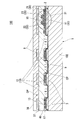
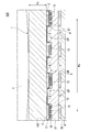
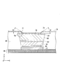
- FIG. 2 is a cross-sectional view showing the sensor unit along the line A-A ′ shown in FIG. 1.
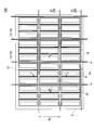
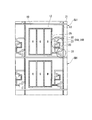
- FIG. 2 is a partially enlarged view showing the configuration of the black matrix substrate according to the first embodiment of the present invention, in which a first conductive pattern of a first conductive layer and a second conductive layer of a second conductive layer disposed on a black dielectric layer. It is a top view showing arrangement of a pattern.
- FIG. 1 is a partially enlarged view showing a configuration of the black matrix substrate according to the first embodiment of the present invention, and is a circuit diagram showing a sensor unit (unit cell) including a capacitor pattern and a thin film transistor (first thin film transistor).
- FIG. 2 is a cross-sectional view showing the sensor unit along
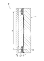
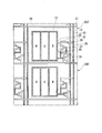
- FIG. 4 is a cross-sectional view showing the sensor unit along the line B-B ′ shown in FIG. 3.
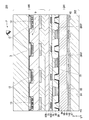
- FIG. 4 is a sectional view showing the sensor unit along the line C-C ′ shown in FIG. 3.
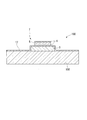
- FIG. 2 is a partially enlarged view showing the black matrix substrate according to the first embodiment of the present invention, and is a cross-sectional view showing a structure of a conductive layer provided on a first insulating layer on a black dielectric layer.
- FIG. 2 is a partially enlarged view illustrating a configuration of the black matrix substrate according to the first embodiment of the present invention, and is a cross-sectional view illustrating a situation when a pointer such as a finger contacts the first surface of the black matrix substrate.
- FIG. 9 is a view showing a black matrix substrate according to a modification of the first embodiment of the present invention, wherein a layer of a resin dispersion having a different carbon concentration is inserted between a second surface and a black dielectric layer; It is sectional drawing explaining the situation of reflection of visible light. It is a circuit diagram showing a sensor unit which constitutes a black matrix board concerning a modification of a 1st embodiment of the present invention. It is a circuit diagram showing a sensor unit which constitutes a black matrix board concerning a modification of a 1st embodiment of the present invention.
- FIG. 4 is a partially enlarged view showing a black matrix substrate according to a modification of the first embodiment of the present invention, in which a first conductive pattern of a first conductive layer and a second conductive pattern of a second conductive layer are provided on a black dielectric layer. It is a top view showing arrangement of a conductive pattern.
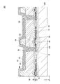
- FIG. 6 is a diagram illustrating a display device according to a second embodiment of the present invention, and is a cross-sectional view partially illustrating a micro LED display device to which the black matrix substrate according to the first embodiment of the present invention is applied.
- FIG. 9 is a view showing a display device according to a second embodiment of the present invention, and is a partial cross-sectional view of an array substrate on which micro LEDs are mounted.
- FIG. 6 is a diagram illustrating a display device according to a second embodiment of the present invention, and is a cross-sectional view partially illustrating a micro LED display device to which the black matrix substrate according to the first embodiment of the present invention is applied
- FIG. 14 is a diagram illustrating a display device according to a second embodiment of the present invention, and is an enlarged cross-sectional view of a region indicated by reference numeral C in FIG. 13.
- FIG. 14 is a diagram illustrating a display device according to a second embodiment of the present invention, and is an enlarged cross-sectional view of a first thin film transistor illustrated in FIG. 13.
- FIG. 9 is a typical circuit diagram including a thin film transistor that drives a micro LED applied to a display device according to a second embodiment of the present invention. It is a figure showing the display concerning a 3rd embodiment of the present invention, and is a sectional view showing a part of an organic EL display to which a black matrix substrate was applied.
- FIG. 14 is a diagram illustrating a display device according to a second embodiment of the present invention, and is an enlarged cross-sectional view of a region indicated by reference numeral C in FIG. 13.
- FIG. 14 is a diagram illustrating a display device according to a second embodiment
- FIG. 10 is a view showing a display device according to a third embodiment of the present invention, and is a partial cross-sectional view of an array substrate on which an organic EL layer is mounted. It is a figure showing the display concerning a 4th embodiment of the present invention, and is a sectional view showing a liquid crystal display to which a black matrix substrate is applied partially.
- FIG. 13 is a typical circuit diagram including a thin film transistor for driving a liquid crystal layer applied to a display device according to a fourth embodiment of the present invention.
- FIG. 4 is a cross-sectional view partially showing a liquid crystal display device employing a conventional horizontal alignment liquid crystal (FFS mode), showing the state of equipotential lines when a liquid crystal driving voltage is applied between a pixel electrode and a common electrode.
- FFS mode horizontal alignment liquid crystal
- FIG. 2 is a cross-sectional view partially showing a liquid crystal display device employing a conventional horizontal alignment liquid crystal (FFS mode), illustrating the state of equipotential lines when a transparent electrode is provided on a transparent resin layer of a substrate. It is sectional drawing.
- FFS mode horizontal alignment liquid crystal
- the phrase “in a plan view from the first surface” refers to a black dielectric layer, a conductive pattern, and a light absorption layer laminated on a second surface (back surface) of a transparent substrate, which are defined by an observer. It means a plan view seen from the first surface. Further, the phrase “in a plan view from the second surface” means that the conductive pattern and the black dielectric layer laminated on the second surface of the transparent substrate are separated from the second surface (the surface opposite to the viewer's view surface). Means a planar view as seen. When the wording “plan view viewed from the first surface” and the word “plan view viewed from the second surface” are substantially equivalent, they are simply referred to as “plan view”.
- first and second are used to avoid confusion between components, and do not limit the number.
- the first conductive pattern and the second conductive pattern may be simply referred to as a conductive pattern or a conductive layer.
- Each of the conductive layers (conductive patterns) has a three-layer structure in which a metal layer or an alloy layer is sandwiched between conductive oxide layers.
- the “display function layer” included in the display device includes a plurality of light-emitting diode elements called LEDs (Light Emitting Diodes) and a plurality of organic ELs (organic electroluminescence) also called OLEDs. Either an element or a liquid crystal layer can be used.
- FIG. 1 is a partially enlarged view showing the configuration of the black matrix substrate according to the first embodiment of the present invention, and is a circuit diagram showing a sensor unit (unit cell) including a capacitor pattern and a thin film transistor (first thin film transistor).
- the minimum element configuration is shown as the configuration of the partition region 19 for easy understanding. That is, FIG. 1 illustrates a minimum element configuration including only one first thin film transistor 31 in the partitioned area 19.
- FIG. 1 shows a circuit diagram, an actual configuration in which the capacitor pattern 12 is formed by the three openings 9, that is, a schematic configuration of the sensor unit, for easy understanding of the following description. Is shown.
- the capacitor pattern 12 is provided in a partition region 19 (region) partitioned by the scanning lines and the output lines.
- the partition region 19 is a region partitioned by the scanning line 13 for driving the thin film transistor and the output line 21 to which an output signal is applied from the thin film transistor.
- a sensor including a conductive layer (conductive pattern) in which a black dielectric layer, a metal layer or an alloy layer is sandwiched between conductive oxides, a light absorbing layer, a thin film transistor, a single capacitor pattern, and the like.
- a unit is defined as a unit cell.
- a plurality of unit cells are arranged in a matrix on a black matrix substrate.
- a sensor unit or a unit cell may be used as a technical term in the description.
- the sensor unit or the unit cell has the same meaning as a region where a capacitor is formed, that is, a region defined by a scanning line and an output line. In plan view, the scanning lines extend parallel to the first direction, and the output lines extend parallel to a second direction orthogonal to the first direction.
- the sensor unit SU includes a first conductive pattern 10, a second conductive pattern 20, and a first thin film transistor 31.
- the first thin film transistor 31 includes a first gate electrode 11, a first source electrode 22, a first drain electrode 23, a first channel layer 16 (described later, an oxide semiconductor layer), and a gate insulating layer (described later, a second insulating layer 48). ).
- the first source electrode 22 is connected to the scanning line 13 via a contact hole 29.
- the first drain electrode 23 is connected to the output line 21.
- the first drain electrode 23 is connected to the output line 21.
- the output line 21, the first source electrode 22, and the first drain electrode 23 form the second conductive pattern 20.
- the second conductive pattern 20 is formed of the second conductive layer
- the first conductive pattern 10 is formed of the first conductive layer.
- the first conductive pattern 10 and the second conductive pattern 20 may be simply referred to as a conductive pattern.
- the first conductive layer and the second conductive layer may be simply referred to as a conductive layer.
- the conductive layer refers to a structure in which a metal layer or an alloy layer is sandwiched between conductive oxide layers, as described later.
- the first gate electrode 11, the capacitor pattern 12 (capacitor electrode), and the scanning line 13 form a first conductive layer having the first conductive pattern 10.
- the capacitor pattern 12 includes one or more openings 9 (first openings) in plan view.
- the shape of the opening 9 is not limited to the rectangle shown in FIG. 1 and may be a parallelogram.
- the capacitor pattern 12 is connected to the first gate electrode 11.
- the capacitor pattern 12 supplies a change in capacitance when a pointer such as a finger contacts or approaches the first surface 1 to the first thin film transistor 31 as a signal.
- the capacitor pattern 12 may be referred to as a capacitor electrode.
- reference characters R, G, and B denote red pixels R of an array substrate facing (attached to) the black matrix substrate when the black matrix substrate is applied to a display device that performs color display. , Green pixel G, and blue pixel B, respectively. That is, the capacitor pattern 12 has a size corresponding to the size of one or more pixels used for display. For example, in the case of displaying an image using three pixels of red, green, and blue, the size of the capacitor pattern may be an integral multiple of three. For example, in the case of displaying an image using four pixels of red, green, blue, and white, the size of the capacitor pattern can be set to an integral multiple of four. In a fourth embodiment described later, a configuration in which a color filter including a red pixel, a green pixel, and a blue pixel is arranged in the opening 9 of the black matrix substrate is illustrated.
- the output line 21, the first source electrode 22, and the first drain electrode 23 form a second conductive layer having the second conductive pattern 20.
- the roles (functions) of the scanning line and the output line can be switched. Further, the roles (functions) of the source electrode and the drain electrode can be interchanged. That is, in FIG. 1, reference numeral 13 may be an output line, reference numeral 21 may be a scanning line, reference numeral 22 may be a first drain electrode, and reference numeral 23 may be a first source electrode.
- the first conductive layer and the second conductive layer have a configuration in which a metal layer or an alloy layer is sandwiched between conductive oxide layers. Since the first gate electrode 11, the capacitor pattern 12, the scanning line 13, and the output line 21 forming the second conductive layer, which constitute the first conductive layer, are made of a metal or alloy having excellent conductivity, they are static. The responsiveness of the capacitance detection and the S / N ratio can be improved. Examples of the metal having high conductivity as described above include silver, copper, and aluminum. In consideration of reliability, a silver alloy, a copper alloy, or an aluminum alloy may be used. By using a conductive layer (conductive pattern) in which a metal layer or an alloy layer is sandwiched between conductive oxide layers as a configuration of the capacitor pattern 12, the scanning line 13, and the output line 21, a plurality of advantages described below can be obtained. Can be
- the capacitance of a pointer such as a finger is large.
- electrostatic breakdown may occur, and chipping or peeling of the copper alloy wiring may occur.
- silver, copper, or a copper alloy has insufficient adhesion to resin or glass.
- a conductive layer in which a metal layer or an alloy layer is sandwiched between conductive oxide layers is employed.
- the conductive oxide has extremely high adhesion to silver, copper, a copper alloy, or the like, and further has extremely high adhesion to resin or glass. Therefore, chipping or peeling of the copper alloy wiring due to electrostatic breakdown hardly occurs.
- Second advantage For example, when silver alloy wiring or copper alloy wiring is adopted as the structure of the conductive layer (in the case of using no conductive oxide), silver or copper diffuses into the resin or glass base material, and the reliability is improved. May cause a decrease. In particular, when the manufacturing process includes a processing step exceeding 250 ° C., copper or a copper alloy is easily oxidized. In contrast, when a conductive layer in which a metal layer or an alloy layer is sandwiched between conductive oxide layers is employed as in the present embodiment, the conductive oxide layer diffuses silver or copper into the glass substrate. Inhibits copper oxidation.
- Silver, copper, or copper alloys are relatively soft metals. For this reason, the wiring made of silver, copper, or a copper alloy is easily damaged during electrical mounting at the end of the touch panel.
- the conductive oxide is also one of the ceramic materials. When the oxide layer sandwiches copper, a silver alloy, or a copper alloy, hard and reliable mounting becomes possible.
- the first source electrode 22 is electrically connected to the scanning line 13 via the contact hole 29.
- a good electrical connection in the contact hole 29 is obtained by the conductive oxide layer.
- a copper oxide is easily formed on the surface of copper or a copper alloy. Copper oxide increases in thickness over time, making electrical packaging unstable. Similarly, oxides and sulfides are easily formed on the surface of silver. In a configuration in which copper or a copper alloy is sandwiched between conductive oxide layers, a conductive oxide layer is formed on the surface of the conductive layer (conductive pattern), and ohmic contact is possible.
- the conductive layer according to the embodiment of the present invention can be applied to a source wiring, a source electrode, a drain electrode, a gate electrode, a gate wiring, and a touch sensing wiring of various TFTs (thin film transistors).
- a mixed oxide containing at least 50 at% of indium oxide can be used.
- a method for forming a three-layer structure in which a copper layer or a copper alloy layer is sandwiched between two conductive oxide layers first, for example, a method in which [mixed oxide layer A / copper alloy layer B / mixed oxide layer C]. Thereafter, the three layers are processed so as to have the same line width by a wet etching process.
- the line width of the mixed oxide layer A, the copper alloy layer B, and the mixed oxide layer C sequentially formed on the surface of the glass substrate by the wet etching process is set to satisfy the condition “line width of mixed oxide layer A>
- line width of mixed oxide layer C In order to satisfy “line width of copper alloy layer B> line width of mixed oxide layer C”, it is necessary to process so that the line width becomes smaller in order.
- ITO mixed oxide containing indium oxide and tin oxide
- copper is selectively etched, and the line width of the three layers does not satisfy the above condition. Therefore, by adding a readily soluble oxide such as zinc oxide, gallium oxide, and antimony oxide to indium oxide, the corrosion potential is adjusted, and a mixed oxide layer having a uniform corrosion potential is obtained.
- the conductive layers (the first conductive layer and the second conductive layer) according to the embodiment of the present invention have a three-layer structure in which the metal layer or the alloy layer is sandwiched between the conductive oxides as described above.
- a metal such as silver, copper, aluminum, or zinc having excellent conductivity, or an alloy layer of the above metals can be used.
- copper and a copper alloy will be described as typical examples, but the basic technical means according to the embodiment of the present invention can also be applied to metals such as silver and zinc.
- an alloy element to be added to copper an alloy element whose specific resistance increase rate of the copper alloy layer is 1 ⁇ cm / at% or less can be selected.
- the specific resistance (electrical resistivity) of the copper alloy layer can be in the range of 1.9 ⁇ cm to 6 ⁇ cm.
- Zinc and calcium can each be added as alloying elements to copper up to 5 at%.
- the conductive layer hardly transmits visible light. Therefore, if the copper layer or the copper alloy layer constituting the conductive layer according to the present embodiment has a thickness of, for example, 100 nm to 500 nm, sufficient light-shielding properties can be obtained.
- the thickness of the copper alloy layer may exceed 500 nm.
- the material of the conductive layer can be applied to wirings and electrodes provided on an array substrate described later.
- a structure of a wiring electrically linked to an active element for example, as a structure of a gate electrode or a gate wiring, a stacked structure in which a copper alloy layer is sandwiched between conductive metal oxide layers.
- a structure can be adopted.
- a laminated structure in which a copper alloy layer is sandwiched between conductive metal oxide layers can be adopted for the conductive layer (conductive pattern) according to the embodiment of the present invention.
- FIG. 2 is a cross-sectional view showing the sensor unit SU (unit cell) along the line AA ′ shown in FIG. FIG. 2 can be restated as a cross-sectional view showing the black matrix substrate 100 according to the embodiment of the present invention.
- the black matrix substrate 100 has a transparent substrate 102 (first substrate) having a first surface 1 and a second surface 2.
- the specific substrate material of the transparent substrate 102 that can be used for the black matrix substrate 100 is not particularly limited as long as it is a material that is transparent in the visible region.
- Various transparent substrates such as sapphire substrates, substrates made of aluminosilicate glass, etc., acrylic substrates, polyester films, polyimide films, TAC films used for polarizing plates, and resin substrates laminated with vinyl chloride used for IC cards Can be used.
- the substrate be a rigid substrate, such as a glass substrate, having a highly planar and highly flat surface.
- the black dielectric layer 3 and the first insulating layer 17 are laminated in this order. That is, the black dielectric layer 3 is provided on the second surface 2, and is formed on the black dielectric layer 3 so as to cover the exposed surface (surface) of the second surface 2 and the surface of the black dielectric layer 3.
- a first insulating layer 17 is provided. Further, a first conductive pattern 10 is provided on the first insulating layer 17.
- the second insulating layer 48 is laminated so as to cover the first conductive pattern 10 (including the first gate electrode 11, the capacitor pattern 12, and the scanning line 13) and the exposed surface (surface) of the first insulating layer 17. That is, the second insulating layer 48 is provided on the first conductive pattern 10.
- a first transparent resin layer 37 (transparent resin layer) is provided on the second insulating layer 48. That is, a transparent resin layer is provided on the second conductive pattern 20 (second conductive layer).
- a light absorbing layer 8 and a second transparent resin layer 38 are laminated on the first transparent resin layer 37.
- the second transparent resin layer 38 covers the exposed surface (surface) of the first transparent resin layer 37 and the light absorbing layer 8.
- First insulating layer As a material of the first insulating layer 17, as described later, silicon dioxide, silicon nitride, or a transparent inorganic oxide or transparent nitride having a high dielectric constant can be applied.
- a material of the first transparent resin layer 37 or the second transparent resin layer 38 an acrylic resin, a polyimide resin, a benzocyclobutene resin, a polyamide resin, or the like may be used.
- a low dielectric material low-k material
- a conductor layer having the same pattern as the first transparent resin layer 37 in plan view may be inserted. This conductor layer may be grounded as necessary to form an auxiliary capacitance between the conductor layer and the capacitor pattern 12.
- the first insulating layer 17 may have a thickness of, for example, 1 nm to 1000 nm.
- the material of the first insulating layer 17 may be an oxide layer containing one or more of silicon dioxide, silicon oxynitride, cerium oxide, and titanium oxide.
- the first insulating layer 17 may be formed of a material having a high dielectric constant at an interface between the capacitor pattern 12 and the first insulating layer 17.
- a material constituting the first insulating layer 17 is not particularly limited, and examples thereof include silicon oxide, silicon oxynitride, and silicon nitride.
- the thickness of the first insulating layer 17 does not need to be limited, but may be, for example, in the range of 1 nm to 1000 nm.
- the black dielectric layer 3 contains carbon.
- the black dielectric layer 3 is composed of a dispersion in which carbon is dispersed in a resin, or a dispersion in which a dielectric which is fine particles of metal oxide or the like is further dispersed in carbon. That is, the black dielectric layer 3 may be composed of a resin dispersion containing carbon and dielectric fine particles composed of at least a metal oxide.
- the black dielectric layer 3 has a configuration that covers the first conductive pattern 10 and the second conductive pattern 20 in plan view. In the following description, the fine particles may be simply referred to as powder.
- the electrical characteristics of the black dielectric layer 3 are adjusted so as to have a high relative dielectric constant of, for example, 10 to 700. It is possible to do.
- the relative dielectric constant of the black dielectric layer 3 can be adjusted to 150 or more by adjusting the dispersion state of carbon or adding fine particles of a ferroelectric substance or fine particles of a paraelectric substance to the black dielectric layer 3. it can.
- the black matrix substrate according to the present embodiment is applied to an electronic device in which an increase in power consumption is a problem due to the dielectric loss (tan ⁇ ) of the black dielectric layer 3 (for example, a mobile device), the black dielectric layer 3 May be suppressed in the range of 15 to 100.
- the black matrix substrate 100 has a configuration in which the black dielectric layer 3 is inserted between the second surface 2 of the transparent substrate 102 and the capacitor pattern 12.
- a material constituting the black dielectric layer 3 according to the embodiment of the present invention a dispersion in which carbon as a black pigment is dispersed in a resin such as acryl, epoxy, or polyimide can be used. Further, carbon nanotubes, carbon nanohorns, carbon nanobrushes and the like may be mixed and dispersed in the resin. Alternatively, a part of the configuration of the black dielectric layer 3 may be replaced with carbon, and the carbon nanotubes may be dispersed in the resin.
- the black dielectric layer 3 may be simply referred to as a black dielectric.
- the black dielectric layer 3 includes calcium oxide, calcium carbonate, barium sulfate, and silicon dioxide for the purpose of adjusting the dispersion state of carbon and adjusting the relative dielectric constant.
- An extender such as kaolin, clay or the like can be added to the black dielectric layer 3.
- a resin dispersion to which a dielectric powder having a high dielectric constant such as titanium oxide, barium titanate, titanium black, barium zirconate, magnesium titanate, or calcium sulfate is added in addition to carbon. it can.
- a dispersion of a resin to which a dielectric powder containing any of titanium oxide, titanium nitride, and titanium oxynitride in addition to carbon can be used.
- a paraelectric for the purpose of improving the dispersion state of carbon in the black dielectric layer 3 and not increasing the dielectric loss.
- the paraelectric has no electric polarization when no electric field is applied, and has a small dielectric loss.
- a metal oxide such as forsterite (MgSiO 2 ), aluminum oxide (Al 2 O 3 ), or titanium oxide (TiO 2 ), which is a paraelectric, can be added to the black dielectric.
- the dielectric constant of a black dielectric obtained by adding a ferroelectric substance to a resin is increased, but the power consumption is increased in the touch drive for performing touch detection.
- a black dielectric obtained by adding a paraelectric substance to a resin and dispersing the resin can increase the amount of change in the capacitance (difference between the capacitance at the time of reset and the capacitance at the time of touch) and suppress power consumption.
- the paraelectric metal oxide is a metal oxide or a metal oxide powder having a relative dielectric constant of 110 or less and a dielectric loss in a range of 0.00001 to 0.1. Define.
- the measurement frequency of these electric characteristics is a touch sensing frequency described below, which is a frequency measured at a room temperature of 20 ° C.
- the black dielectric layer 3 is composed of a dispersion in which fine particles of a metal oxide such as carbon or titanium oxide are dispersed in a resin and has a relative dielectric constant of 10 to 700 or 15 to 100. ing.
- the dielectric loss (tan ⁇ ) of the dispersion (solid) of the black dielectric layer 3 may be in the range of 0.005 to 0.2 at the touch sensing frequency in the range of 200 Hz to 500 KHz, for example. Further, the value of the dielectric loss is preferably equal to or less than 0.08.
- the resistivity of the black dielectric layer 3 may be adjusted so that the reset ends. In other words, in order to set a reset potential such as ground, for example, the resistivity of the black dielectric can be set to less than 1 ⁇ 10 13 ⁇ cm, and the relaxation time (or time constant) can be shortened.
- the resistivity of the black dielectric may be 1 ⁇ 10 13 ⁇ cm or more.
- the resistivity of the black dielectric is 1 ⁇ 10 14 ⁇ cm or more, there is a possibility that the above relaxation time is adversely affected. Therefore, the technical value of making the resistivity of the black dielectric 1 ⁇ 10 14 ⁇ cm or more is low.
- the electrical characteristics of the black dielectric can be variously adjusted according to the content of touch sensing as described above.
- the fine particles are fine particles having an average particle size in the range of 0.02 to 2 ⁇ m.
- the light absorbing layer 8 may be, for example, a light absorbing layer having an optical density in a range of 1 to 4.
- a dispersion in which a black pigment such as carbon is dispersed in a transparent resin such as an acrylic resin may be used as the light absorbing layer 8.
- the electrical characteristics such as the dielectric constant of the light absorbing layer may be different from or the same as the black dielectric layer 3 described above.
- the light absorbing layer 8 has a configuration that covers the first conductive pattern 10 and the second conductive pattern 20 in plan view.
- the light absorption layer 8 illustrated in FIG. 2 is formed by forming a metal layer on a light-emitting element such as a channel layer of a thin film transistor or a diode provided on the array substrate. This is provided for the purpose of preventing the reflected light from the conductive pattern from entering. Since the channel layer and the light emitting element are made of a semiconductor that senses light, the light absorbing layer 8 is provided for the purpose of preventing malfunction of the channel layer and the light emitting element.
- the light absorbing layer 8 contains a light absorbing agent such as carbon or an organic pigment. In order to reduce the parasitic capacitance, it is preferable that the structure of the light absorption layer does not include a ferroelectric substance.
- the black dielectric layer 3 and the light absorbing layer 8 are formed so as to have an opening pattern having a plurality of openings OP (second openings).
- the opening OP has a shape similar to the opening 9. That is, in the present embodiment, the opening OP has a rectangular shape, like the opening 9. If the shape of the opening 9 is a parallelogram, the shape of the opening OP is also a parallelogram. The center position of the opening OP overlaps the center position of the opening 9.
- the first thin film transistor 31 is formed on the first insulating layer 17 together with the first gate electrode 11 (see FIG. 1).
- a second insulating layer 48 functioning as a gate insulating layer is provided on the first gate electrode 11 (first conductive pattern 10).
- the first channel layer 16, the first source electrode 22 (the second conductive pattern 20), and the first drain electrode 23 (the second conductive pattern 20) are provided on the second insulating layer 48.
- the first source electrode 22 and the first drain electrode 23 are formed not only on the second insulating layer 48 but also on the first channel layer 16.
- the first source electrode 22 and the first drain electrode 23 are formed so as to cover portions located on both sides of the first channel layer 16. 2, the first source electrode 22 covers the left end of the first channel layer 16, and the first drain electrode 23 covers the right end of the first channel layer 16.
- the first channel layer 16 is formed using an oxide semiconductor.
- the first thin film transistor 31 shown in FIG. 2 has a bottom gate structure, but may have a top gate structure.
- the first thin film transistor having a top gate structure can be formed by changing the order of forming the first conductive pattern 10, the second conductive pattern 20, and the like.
- the oxide semiconductor that can be used for the first channel layer 16 included in the oxide semiconductor layer is selected from two or more of indium oxide, zinc oxide, gallium oxide, silicon oxide, antimony oxide, bismuth oxide, cerium oxide, and tin oxide.
- the oxide semiconductor layer may include indium oxide and at least one of antimony oxide and bismuth oxide.
- the oxide semiconductor layer may include at least one of cerium oxide and tin oxide.
- An oxide semiconductor in which at least one of antimony oxide and bismuth oxide is added to indium oxide has an advantage that it can be crystallized by low-temperature annealing at 340 ° C. or lower.
- Heat treatment at a temperature exceeding 350 ° C. has a problem that copper contained in the structure of the conductive layer (conductive pattern) diffuses. The diffusion of copper causes a problem of an increase in the resistance value of the copper wiring and impairs the characteristics of the thin film transistor. For this reason, it is preferable to employ an oxide semiconductor that crystallizes by annealing at 350 ° C. or lower.
- the first thin film transistor 31 uses an oxide semiconductor that can be formed by forming the first channel layer 16 at a low temperature. Therefore, a resin substrate having poor heat resistance as described above can be applied to the transparent substrate 102.
- the semiconductor forming step includes a laser annealing step of heating at about 600 ° C.
- a structure in which a channel layer is formed of an amorphous silicon semiconductor or a structure in which a channel layer is formed of a polysilicon semiconductor is known.
- the electron mobility is low, and it is insufficient as a semiconductor for a touch sensor.
- the polysilicon semiconductor has a high electron mobility, but has a drawback that the performance of a transistor is such that a leakage current is large and it is difficult to maintain a capacitance at the time of touch sensing.
- both the amorphous silicon semiconductor and the polysilicon semiconductor have a low electric breakdown voltage, and have a disadvantage that the transistor is destroyed depending on the degree of change in the capacitance during touch sensing.
- the oxide semiconductor according to this embodiment has an electric breakdown voltage that is 100 times or more higher than that of a silicon-based semiconductor, and also has a high electron mobility.
- An oxide semiconductor is preferably used as a channel layer of a thin film transistor for driving a touch sensor.
- FIG. 3 is a partially enlarged view showing the configuration of the black matrix substrate 100.
- the capacitor pattern 12 and the scanning line 13 constituting the first conductive pattern 10 laminated on the black dielectric layer 3 and the second conductive pattern are shown in FIG.
- FIG. 3 is a plan view showing output lines 21 constituting the first embodiment.
- FIG. 3 is a plan view of the transparent substrate 102 as viewed from the second surface 2, but does not show the light absorbing layer 8 and the first thin film transistor 31.
- the plurality of openings 9 illustrated in FIG. 3 correspond to light emission portions of a display device to which the black matrix substrate 100 is applied.
- a display device configured by bonding a black matrix substrate 100 according to an embodiment of the present invention and an array substrate on which an active element such as a TFT (Thin Film Transistor) is formed via a display function layer.
- the plurality of openings 9 are light emission portions.
- the capacitor pattern 12 is formed in a partitioned area 19 defined by the scanning line 13 and the output line 21. Note that the capacitor pattern 12 ′ located at the outermost periphery of the display effective area in the display device does not need to be completely partitioned by the scanning lines 13 and the output lines 21.
- FIG. 4 is a sectional view showing the sensor unit SU along the line BB 'shown in FIG.
- FIG. 5 is a cross-sectional view showing the sensor unit SU along the line CC ′ shown in FIG. 4 and 5 show one display unit having a width Px and a length Py.
- the display unit includes three openings 9.
- the number of openings 9 included in the capacitor pattern 12 can be, for example, a multiple of 3 or 4. Further, the number of the openings 9 may be one or more, and two openings 9 may be provided in one partition region 19 as shown in a modified example described later. Since the capacitance of the capacitor pattern 12 is proportional to the area of the capacitor pattern 12, the number of the openings 9 can be set to two or more, and further to a multiple of three or four.
- a color display in a display device is composed of three pixels of RGB (red pixel, green pixel, blue pixel) or four pixels of RGBW (red pixel, green pixel, blue pixel and further white pixel) and one display unit. Is often configured. Therefore, setting the number of openings 9 by a multiple of 3 or 4 is advantageous in relation to the display unit and the capacitor pattern 12.
- the number of the openings 9 is reduced by 1 in accordance with the necessity of reducing the parasitic capacitance between the scanning line 13 for performing touch sensing and the capacitor pattern 12 (in other words, the necessity of adjusting the distance between wirings).
- the number may be two or more or two or more.
- a color filter substrate is realized by adding a color filter of red pixel R, green pixel G, and blue pixel B to each of the plurality of openings 9. be able to.
- a protective glass cover glass
- the black matrix substrate 100 shown in FIG. 4 via the second transparent resin layer 38 (adhesive layer), and the black matrix substrate 100 may be used as a touch panel. .
- the relative permittivity of a glass or resin substrate serving as a support for supporting a transparent electrode such as ITO is often in the range of about 3 to 6.
- the electrode ECS (light-transmitting conductive film) disclosed in FIG. 2 of Patent Document 2 is in contact with a glass or resin substrate 62 as described in paragraph [0054].
- a transparent electrode such as ITO is used as a capacitor electrode (capacitor pattern) as a capacitance detecting element
- the relative permittivity of glass and resin is small, and is not a preferable material.
- ITO has a resistivity of about 2 ⁇ 10 ⁇ 4 ⁇ cm.
- copper which is a metal
- a metal such as silver, copper, aluminum, or zinc, or an alloy containing the above materials, as the material of the capacitor electrode (capacitor pattern), the scanning line, and the output line, which are the capacitance detection elements.
- FIG. 6 is a partially enlarged view showing the black matrix substrate 100, and is a partial cross-sectional view showing a configuration in which a black dielectric layer 3, a first insulating layer 17, and a conductive layer 7 are laminated in this order on a transparent substrate 102. is there.
- the conductive layer 7 has a three-layer structure in which the metal layer 5 is sandwiched between the conductive oxide layers 4.
- the metal layer 5 shown in FIG. 6 may be an alloy layer. As described above, the metal layer 5 and the alloy layer can be a copper layer or a copper alloy layer. The thicknesses of the two layers located above and below the conductive oxide layer 4 may be different. Note that the configuration of the conductive layer 7 can be applied to the above-described second conductive layer.
- FIG. 7 is a partially enlarged view showing the configuration of the black matrix substrate 100, and is a cross-sectional view illustrating a situation when a pointer such as a finger F contacts the first surface 1 of the black matrix substrate 100.
- a pointer such as a finger F contacts the first surface 1 of the black matrix substrate 100.
- the capacitor pattern 12 detects a change in capacitance together with the black dielectric layer 3.
- the capacitor pattern 12 sends a touch detection signal to the output line 21 via the first thin film transistor 31.
- the change in the capacitance (the amount of change in the capacitance and the change in the potential) detected by the capacitor pattern 12 is input to the first gate electrode 11 of the first thin film transistor 31.
- the scanning line 13 (the scanning line can be referred to as a power supply line) sends a selection signal to the first thin film transistor 31 provided in the sensor unit SU.
- the amount of change in capacitance input to the first gate electrode 11 is amplified by the first thin film transistor 31 and output to the output line 21.
- a control unit (not shown) connected to the output line 21 detects the touch detection signal and performs touch sensing.
- the fingerprint density of a finger is about 3 / mm.
- a touch panel with a resolution of about 10 / mm to 100 / mm can perform fingerprint authentication.
- the black matrix substrate 100 according to the present embodiment may have a resolution of 100 lines / mm or more. In the case of pen input, a resolution of several tens of microns corresponding to the pen tip is sufficient.
- the black matrix substrate 100 according to the present embodiment is applied to a smartphone, a tablet terminal, or the like corresponding to a pixel resolution exceeding 400 ppi, a touch resolution exceeding 100 lines / mm is possible.
- the width Px of the capacitor pattern 12 corresponding to these three pixels is three pixels The equivalent of 45 ⁇ m. If the unit cell width (synonymous with the unit cell pitch or the size of the display unit) of the touch sensor is 45 ⁇ m, fingerprint authentication and pen input can be sufficiently performed. Since the pitch of the unevenness of the fingerprint (ridge line and valley line of the fingerprint) is approximately 3 lines / mm, the capacitor pattern 12 only needs to have a resolution of, for example, about 10 lines / mm to 100 lines / mm. Thereby, fingerprint authentication is possible.
- the black dielectric layer 3 stores electric charges and functions as an electrostatic capacitor (capacitance) element. If the pointer is a pen tip, a change in capacitance occurs in the black dielectric layer 3 having a size close to the area of the pen tip. When the finger F presses the first surface 1 with a strong pressure, a change in capacitance occurs in the number of black dielectric layers 3 corresponding to the contact area of the finger F.
- a fingerprint pattern is two-dimensionally detected in accordance with the unevenness of the fingerprint (valley line: valley @ line, ridge line: ridge @ line).
- a distance Pz from the black dielectric layer 3 to the finger F shown in FIG. 7 may be practically in the range of about 0.1 mm to 1.5 mm.
- the distance Pz may include, for example, the thickness of a cover glass for protection and the thickness of a polarizing plate or a retardation plate. Due to the configuration of the black dielectric layer 3 having a high relative dielectric constant and the metal layer 5 (or an alloy layer) having a high electrical conductivity according to the embodiment of the present invention, the transparent substrate 102 has a thickness exceeding 0.4 mm. Even so, fingerprint authentication is possible.
- the most typical metal layer 5 (or alloy layer) material is copper and copper alloy.
- FIG. 8 is a cross-sectional view showing a black dielectric layer 3 constituting a black matrix substrate according to a modification of the first embodiment.
- FIG. 4 is a cross-sectional view illustrating a state of reflection of visible light when inserted between the body layer 3 and the body layer 3.
- the black dielectric layer is composed of two resin dispersions (black dielectric layer 3 and low-concentration carbon layer 6) having different carbon concentrations. At least one of the two layers of the resin dispersion contains a dielectric made of a metal oxide.
- the effective optical density of the low-concentration carbon layer 6 is set, for example, in the range of 0.05 to 0.4.
- the thickness of the low-concentration carbon layer 6 may be set in the range of 0.1 ⁇ m to 0.7 ⁇ m.
- the effective optical density of the black dielectric layer 3 is set, for example, in a range of 0.5 or more and less than 3.
- the thickness of the black dielectric layer 3 may be set in the range of 0.5 ⁇ m to 2 ⁇ m.
- the optical density of the black dielectric layer 3 may be set to a value exceeding 3, but setting the optical density of the black dielectric layer 3 in contact with the metal layer or the alloy layer to 3 or more has no technical meaning.
- the thickness of the low-concentration carbon layer 6 may be greater than 0.8 ⁇ m, but increasing the thickness of the low-concentration carbon layer 6 has little technical significance.
- the reflectance of visible light between the second surface 2 and the black dielectric layer 3 as viewed from the first surface 1 (viewing direction) is 0.4%. It can be: This low reflectance of 0.4% or less is a substantially flat reflectance between light wavelengths of 400 nm to 700 nm, and is different from a low reflection film of an ordinary optical multilayer. With an optical multilayer low-reflection film having a configuration in which SiO 2 / TiO 2 and the like are stacked, it is difficult to obtain a flat low reflectance in a wide wavelength range.
- the reflectance is a ratio of the reflected light 34 to the incident light 33 from the outside.
- the reflected light 34 is light that reflects the incident light 33 at the interface between the low-concentration carbon layer 6 and the second surface 2.
- the measurement of the reflectance can be performed using a microspectroscope.
- the chromaticity observed between the black dielectric layer 3 and the second surface 2 and the chromaticity observed between the low-concentration carbon layer 6 and the two layers of the black dielectric layer 3 that is, The chromaticity observed on the second surface 2 falls within a small numerical value of ⁇ 2.0 or less, and becomes a neutral color without coloring.
- the reflectance at the interface between the single layer of the black dielectric layer 3 and the second surface can be set to about 3%.
- the configuration of the black dielectric layer 3 a multilayer configuration having different electrical characteristics such as relative permittivity and resistivity can be adopted.
- electrical characteristics such as relative permittivity and resistivity can be changed in the normal direction from the pointer of the finger F or the like, that is, in the thickness direction of the black dielectric layer 3.
- the relative permittivity of the black dielectric located near the capacitor pattern 12 may be increased, and the relative permittivity of the black dielectric located far from the capacitor pattern may be decreased.
- the concentration of carbon contained in the black dielectric layer 3 may be adjusted in the thickness direction of the black dielectric layer 3. Further, the dispersion state of carbon may be changed along the thickness direction of the black dielectric layer 3.
- the black dielectric layer 3 may have a dielectric constant gradient along the thickness direction. Near the interface between the capacitor pattern 12 and the first insulating layer 17, the black dielectric layer 3 may have a partially high dielectric constant.
- a substrate having a low relative dielectric constant and a material having a relative dielectric constant of 8 or less can be used as the transparent substrate 102.
- the relative permittivity of the transparent substrate 102 may be, for example, 5 or less.
- the reset for example, ground
- the reset period can be shortened by setting the resistivity of the black dielectric layer 3 to 10 8 ⁇ cm or more and less than 10 13 ⁇ cm.
- FIG. 9 is a circuit diagram illustrating a sensor unit included in a black matrix substrate according to Modification 2 of the first embodiment.
- the black matrix substrate according to the second modification includes a sensor unit SU1.
- the sensor unit SU1 includes a reset transistor 32 (second thin film transistor) in addition to the configuration of the sensor unit SU including the first thin film transistor 31 illustrated in FIG.
- the reset transistor 32 includes a second gate electrode 27 electrically connected to the first gate electrode 11, a second source electrode 25, and a second drain electrode 26 electrically connected to the second gate electrode 27 (short-circuited to the second gate electrode 27).
- Part of the first conductive pattern 10 forms the second gate electrode 27.
- Part of the second conductive pattern 20 forms a second source electrode 25 and a second drain electrode 26.
- Part of the oxide semiconductor layer forms the second channel layer 24A.
- Part of the second insulating layer 48 constitutes the gate insulating layer 24B of the second thin film transistor.
- the second channel layer 24A is formed at the same time when the first channel layer 16 is formed.
- the gate insulating layer 24B is formed simultaneously with the formation of the second insulating layer 48.
- the scanning line 13 not only supplies a scanning signal to the first source electrode 22 of the first thin film transistor 31, but also supplies a reset signal (for example, a ground potential) to the reset transistor 32.
- a reset signal for example, a ground potential
- the supply of such a scanning signal and the supply of a reset signal are performed by time division.
- the reset transistor 32 receives a reset signal from the scanning line 13 and resets the potential of the capacitor pattern 12.
- FIG. 10 is a circuit diagram illustrating a sensor unit included in a black matrix substrate according to Modification 3 of the first embodiment. 10, the same members as those of the sensor unit SU1 shown in FIG. 9 are denoted by the same reference numerals, and the description thereof will be omitted or simplified.
- the black matrix substrate according to the third modification includes a sensor unit SU2.
- the sensor unit SU2 includes, in addition to the configuration of the sensor unit SU including the first thin film transistor 31 shown in FIG. 1, a reset transistor 32 shown in FIG. 9 and a source extension 28 extending the second source electrode 25 of the reset transistor 32. And a reset line 15.
- the reset line 15 supplies a reset signal to the reset transistor 32 via the second source electrode 25 and the source extension 28.
- the source extension 28 is not connected to the scanning line 13, but is connected to the reset line 15 via the contact hole 29.
- the sensor unit SU2 can receive the reset signal from the reset line 15 independently of the scan signal from the scan line 13. In the sensor unit SU2, it is not necessary to supply the scanning signal and the reset signal as shown in FIG. As in the case of the sensor unit SU shown in FIG.
- FIG. 1 is a circuit diagram in which one sensor unit includes one thin film transistor.
- 9 and 10 are circuit diagrams in which one sensor unit includes two thin film transistors. However, the number of thin film transistors in one sensor unit can be increased as needed.
- FIG. 11 is a partially enlarged view showing a black matrix substrate according to Modification 4 of the first embodiment, and shows the arrangement of the first conductive pattern 10 and the second conductive pattern 20 provided on the black dielectric layer 3.
- FIG. FIG. 11 shows a modification of the capacitor pattern 12 shown in FIG. 3, and shows a case where two openings 9 are formed in the partition region 19.
- the line widths of the conductive lines B1, B2, and B3 forming a part of the capacitor pattern 12 may be different from each other.
- FIG. 12 is a view showing a display device according to the second embodiment of the present invention, and is a cross-sectional view partially showing a micro LED display device 200 to which the black matrix substrate 100 according to the first embodiment is applied. .
- the second surface 2 of the black matrix substrate 100 faces the second array substrate 201.
- the light emitting elements CHIP are arranged on the surface of the second array substrate 201 facing the second surface 2.
- the black matrix substrate 100 and the second array substrate 201 are bonded via an adhesive layer 108 made of a transparent resin.
- the sensor unit SU (unit cell, see FIG. 1) of the black matrix substrate 100 includes the capacitor pattern 12 and the first thin film transistor 31, and employs the individual reading method.
- the technique using such an individual reading method is a technique close to the self-capacitance method.
- Patent Literature 3 and Patent Literature 4 exemplified as the prior art of the display device each use a mutual capacitance method using X-direction wiring and Y-direction wiring, and the capacitance by touch sensing is used. Is greatly different from the second embodiment.
- the capacitive element CS1 having a capacitance includes an electrode ECS, which is a light-transmitting conductive film, an electrode COM, and an insulating layer.
- Patent Document 2 does not disclose a configuration in which a black dielectric is laminated on a copper wiring.
- FIG. 13 is an enlarged view partially showing the second array substrate 201 included in the micro LED display device 200 according to the second embodiment, and is a cross-sectional view partially showing the third thin film transistor 68.
- FIG. 14 is a cross-sectional view showing a light-emitting element (micro LED) mounted on the micro LED display device 200 according to the second embodiment, and is an enlarged view partially showing a region indicated by reference numeral C in FIG.
- FIG. 15 is an enlarged cross-sectional view illustrating the micro LED display device 200 according to the second embodiment, in which the third source electrode 54 stacked on the third channel layer 58 of the third thin film transistor 68 illustrated in FIG.
- FIG. 3 is a diagram illustrating a laminated structure of a three drain electrode 56.
- the material forming the second substrate 202 of the second array substrate 201 does not need to be limited to a transparent substrate.
- a substrate applicable to the second substrate 202 a glass substrate, a ceramic substrate, a quartz substrate, a sapphire substrate, a semiconductor substrate of silicon, silicon carbide, silicon germanium, or the like, a plastic substrate, or the like can be given.
- the second substrate 202 may be a transparent substrate, an opaque substrate, or a colored substrate.
- 4A fourth insulating layer 47 is formed on the surface 43 of the second substrate 202.
- the third thin film transistor 68, the third insulating layer 148 formed so as to cover the fourth insulating layer 47 and the third thin film transistor 68, and the third channel layer 58 of the third thin film transistor 68 are opposed.
- the first flattening layers 96 formed as described above are sequentially stacked.
- a contact hole 93 is formed in the first planarization layer 96, the sixth insulating layer 49, and the third insulating layer 148 at a position corresponding to the third drain electrode 56 of the third thin film transistor 68.
- a bank 94 (see FIG. 13) is formed on the first planarization layer 96 at a position corresponding to the third channel layer 58.
- the upper surface of the first planarization layer 96, the inside of the contact hole 93, and the third drain electrode A reflection electrode 89 (pixel electrode) is formed so as to cover 56.
- the reflection electrode 89 may not be formed on the upper surface of the bank 94.
- the reflection electrode 89 is electrically connected to the lower electrode 88 of the light emitting element CHIP via the conductive bonding layer 77.
- a second planarization layer 95 is formed so as to fill the inside of the contact hole 93 and to cover the reflective electrode 89 and the light emitting element CHIP.
- a transparent conductive film 76 called ITO is formed, and the transparent conductive film 76 (synonymous with the second power supply line 52) has an upper electrode 87 constituting the light emitting element CHIP. Is connected.
- an auxiliary conductor 75 is formed on the transparent conductive film 76, and the transparent conductive film 76 is electrically connected to the auxiliary conductor 75.
- a sealing layer 109 is formed on the surface of the transparent conductive film 76 so as to cover the auxiliary conductor 75.
- the auxiliary conductor 75 is a conductor for reducing the resistance value of the transparent conductive film 76 in plan view.
- an organic resin such as an acrylic resin, a polyimide resin, and a novolak phenol resin can be used.
- an inorganic material such as silicon oxide or silicon oxynitride may be further laminated.
- an acrylic resin, a polyimide resin, a benzocyclobutene resin, a polyamide resin, or the like may be used as a material of the first flattening layer 96 and the second flattening layer 95.
- a low dielectric constant material (low-k material) can also be used as a material of the first flattening layer 96 and the second flattening layer 95.
- any one of the first planarization layer 96, the second planarization layer 95, and the sealing layer 109 may have a light scattering function in order to improve visibility.
- the reflection electrode 89 is in contact with the third drain electrode 56 (fourth wiring).
- the reflective electrode 89 has a conductive metal oxide layer as an upper layer, and the third drain electrode 56 is in contact with the conductive metal oxide layer.
- the reflective electrode 89 has a three-layer structure in which a silver alloy is sandwiched between conductive metal oxide layers.
- Each of the conductive metal oxide layer of the reflective electrode 89 and the conductive metal oxide layer of the third drain electrode 56 is formed of a conductive metal oxide, and can make ohmic contact.
- the surface in contact with the reflective electrode 89 in the contact hole 93 is an oxidized copper surface or aluminum, it is difficult to obtain an ohmic contact.
- Aluminum has insufficient physical adhesion to a conductive metal oxide such as ITO.
- the configuration employed in the micro LED display device 200 according to the second embodiment can provide a wiring structure capable of making ohmic contact in this manner.
- the light emitting element CHIP is a vertical light emitting diode that functions as a display function layer, and is provided for each of a plurality of pixels located on the second substrate 202.
- the light-emitting element CHIP has a structure in which an upper electrode 87, an n-type semiconductor layer 90, a light-emitting layer 92, a p-type semiconductor layer 91, and a lower electrode 88 are stacked in this order.
- the light emitting element CHIP has a configuration in which the p-type semiconductor layer 91, the light-emitting layer 92, the n-type semiconductor layer 90, and the upper electrode 87 are stacked on the lower electrode 88 in this order.
- electrodes used for LED light emission are formed on different surfaces, and are formed on surfaces facing each other.
- an upper electrode 87 and a lower electrode 88 are arranged outside the surfaces facing the n-type semiconductor layer 90 and the p-type semiconductor layer 91 which are stacked so as to be parallel to each other.
- the light emitting element CHIP having such a structure is referred to as a vertical light emitting diode. If the LED structure has a different shape such as a pyramid shape in cross-sectional view, it is not included in the vertical light emitting diode of the present invention.
- a structure in which electrodes are arranged on one surface or a structure in which electrodes are arranged in a horizontal direction is called a horizontal light emitting diode.
- the transparent conductive film 76 overlaps the upper electrode 87 and is electrically connected.
- the corner 74 of the light emitting element CHIP is covered with the second planarization layer 95.
- an overlapping portion 71 where the second planarization layer 95 and the upper electrode 87 overlap is formed. Since the overlapping portions 71 are formed at both ends of the upper electrode 87, the second flattening layer 95 has a concave shape on the upper electrode 87.
- the second planarization layer 95 formed on the upper electrode 87 has a taper with an angle ⁇ in order to reduce the risk of disconnection of the transparent conductive film 76.
- a transparent conductive film 76 is formed along the tapered surface of the second planarization layer 95.
- the overlapping portion 71 is located between the transparent conductive film 76 and the upper electrode 87 at the corner portion 74 and is inclined with respect to the surface of the upper electrode 87 at an angle ⁇ of, for example, 5 ° to 70 °. are doing. Since the overlapping portion 71 has such an inclination, disconnection of the transparent conductive film 76 can be prevented.
- the transparent conductive film 76 is formed. Is liable to be disconnected, and there is a concern that lighting failure of the light emitting element CHIP may occur.
- known photolithography As a method of forming the second planarization layer 95 having the above-described concave shape and a method of forming the overlapping portion 71 overlapping the light emitting element CHIP, known photolithography is employed. Further, a dry etching technique may be applied in addition to a known photolithography technique.
- the shape of the light emitting element CHIP for example, a square shape having a side length of 3 ⁇ m to 500 ⁇ m in plan view can be applied. However, shapes other than squares and rectangles may be applied. Alternatively, the size of one side may be 500 ⁇ m or more.
- one or two or more light-emitting elements can be mounted on a pixel partitioned by the third gate wiring 69 and the third source wiring 66 (see FIG. 16).
- the direction of the square light emitting element CHIP can be randomly rotated in units of 90 degrees. By performing random mounting, it is possible to reduce color unevenness and brightness unevenness of the entire screen caused by slight variations in LED crystal growth.
- a constituent material of the lower electrode 88 silver, a silver alloy, aluminum, or an aluminum alloy can be used. Further, as a configuration of the lower electrode 88, a configuration in which a silver or silver alloy layer is sandwiched between conductive metal oxide layers may be applied, as described later. Part of the configuration of the lower electrode 88 includes a metal layer such as a Ti layer, a Cr layer, a Pt layer, an AuGe layer, a Pd layer, a Ni layer, a TiW layer, a Mo layer, and the above-described conductive metal oxide layer. A multilayer configuration may be introduced. Note that a transflective or transmissive display device can be realized by reducing the area ratio of the lower electrode 88 in a plan view.
- the upper electrode 87 preferably has a configuration including a layer formed of a conductive metal oxide.
- a conductive metal oxide it is preferable that at least the surface layer of the upper electrode 87 is formed of a conductive metal oxide.
- the conductive metal oxide forming the surface layer of the upper electrode 87 be electrically connected to the conductive layer formed of the conductive metal oxide.
- the bonding layer 77 can be formed of, for example, a conductive material capable of fusing the lower electrode 88 and the reflective electrode 89 of the light emitting element CHIP within a temperature range of 150 ° C. to 340 ° C. and making an electrical connection.
- a conductive aggregate such as silver, carbon, and graphite may be dispersed in the heat-flowable resin.
- the bonding layer 77 may be made of In (indium), InBi alloy, InSb alloy, InSn alloy, InAg alloy, InGa alloy, SnBi alloy, SnSb alloy, or the like, or a ternary or quaternary low-melting metal. Can be formed.
- the lower electrode 88 and the reflective electrode 89 are self-aligned. Can be fused.
- various energies such as heat, pressurization, electromagnetic waves, laser light, and a combination of these and ultrasonic waves are used. It should be noted that the vertical light emitting diode has an advantage that repair can be easily performed when a bonding failure occurs.
- the position of the light emitting diode is reduced by reducing the contact angle (wetting property) between the lower electrode 88 and the reflective electrode 89 and the bonding layer 77 to be melted by heating. Matching is possible.
- a horizontal type light emitting diode in which electrodes are arranged in the same direction at the lower part, there are disadvantages that it is difficult to perform a junction inspection of individual diodes and that electrodes are easily short-circuited at the time of repair (replacement of a defective diode or the like). From this viewpoint, a vertical light emitting diode is preferably used.
- the bonding layer 77 can be patterned by a well-known photolithography method or lift-off means.
- FIGS. 13 and 15 show an example of the structure of a thin film transistor (TFT) having a top gate structure used as the third thin film transistor 68 connected to the reflective electrode 89 (pixel electrode).
- the structure of the third thin film transistor 68 is also applied to a fourth thin film transistor 67 described later.
- the third thin film transistor 68 has a configuration in which a third source electrode 54 and a third drain electrode 56 are stacked on a third channel layer 58.
- the third thin film transistor 68 includes a third drain electrode 56 connected to one end of the third channel layer 58 (the left end of the third channel layer 58 in FIG. 15) and the other end of the third channel layer 58 (see FIG. 15, a third source electrode 54 connected to the third channel layer 58 (right end of the third channel layer 58), and a third gate electrode 55 disposed opposite to the third channel layer 58 via the gate insulating layer (third insulating layer 148).
- Third gate electrode 55 has the same configuration as conductive layer 7 shown in FIG. That is, the third gate electrode 55 has a three-layer structure in which the metal layer 5 (alloy layer) is sandwiched between the conductive oxide layers 4.
- the overlapping portion 161 which is an interface where the third channel layer 58 contacts the third source electrode 54 and the interface where the third channel layer 58 contacts the third drain electrode 56 are formed.
- a certain overlapping portion 162 is formed.
- the contact resistance at the interface between the third channel layer 58 and the conductive oxide layer 4 is small, and an ohmic contact can be obtained.
- the conductivity of the conductive oxide layer 4 is high, a conductive metal oxide having substantially high mobility is formed on the third channel layer 58. As a result, transistor characteristics can be improved.
- the conductive oxide layer 4 serves as a high mobility semiconductor layer of the third channel layer 58.
- the third channel layer 58 is made of an oxide semiconductor and is in contact with the third insulating layer 148 which is a gate insulating layer.
- the third thin film transistor 68 drives the light emitting element CHIP.
- the figure does not have a tapered surface.
- a tapered surface inclined surface is formed on an electrode or a channel layer constituting the third thin film transistor 68.
- FIG. 13 shows a structure in which the third channel layer 58, the third source electrode 54, and the third drain electrode 56 of the third thin film transistor 68 are formed on the fourth insulating layer 47. Does not limit such a structure.
- the third thin film transistor 68 may be formed directly on the second substrate 202 without providing the fourth insulating layer 47. Further, a thin film transistor having a bottom gate structure may be applied.
- the third source electrode 54 and the third drain electrode 56 shown in FIG. 13 are formed simultaneously in the same step.
- the third source electrode 54 and the third drain electrode 56 include conductive layers having the same configuration. That is, in the second embodiment, each of the third source electrode 54 and the third drain electrode 56 has a three-layer structure in which a copper or copper alloy layer is sandwiched between conductive oxide layers.
- the third source electrode 54 and the third drain electrode 56 may have a three-layer structure of titanium / aluminum alloy / titanium, molybdenum / aluminum alloy / molybdenum, or the like.
- the aluminum alloy is a typical alloy of aluminum-neodymium.
- a back gate electrode may be provided to stabilize the threshold voltage (Vth) of the third thin film transistor 68 or to obtain stable normally-off transistor characteristics.
- the back gate electrode is formed by patterning a metal film on the opposite side of the third channel layer 58, for example, on the interface between the fourth insulating layer 47 and the second substrate 202 so as to face the third gate electrode 55 shown in FIG. Thus, a back gate electrode can be formed.
- the back gate electrode By forming the back gate electrode with a metal film, the incidence of external light toward the third channel layer 58 can be prevented, and a stable “positive (plus)” Vth can be obtained. Note that a negative voltage is usually applied to the back gate electrode.
- the third channel layer 58 can be electrically surrounded by an electric field formed between the third gate electrode 55 and the back gate electrode.
- the drain current of the third thin film transistor 68 can be increased, and the leak current, which is the off current of the third thin film transistor 68, can be further reduced. Therefore, the relative size of the third thin film transistor 68 can be reduced with respect to the drain current required for the third thin film transistor 68, and the degree of integration as a semiconductor circuit can be improved.
- a thin film transistor including a channel layer formed using an oxide semiconductor has extremely low leakage current, and thus has high stability after input of a scanning signal or a video signal.
- a thin film transistor including a channel layer formed using a polysilicon semiconductor has a larger leakage current by two digits or more than a transistor including an oxide semiconductor. It is preferable that the leakage current is small because it contributes to high-accuracy touch sensing.
- IG IGZO indium oxide, zinc oxide, and gallium oxide
- An oxide semiconductor called IGZO is formed collectively by vacuum film formation such as sputtering. After the oxide semiconductor is formed, heat treatment after pattern formation of a TFT or the like is also performed at one time. For this reason, variations in electrical characteristics (for example, Vth) related to the channel layer are extremely small. In driving the LED, it is necessary to suppress the variation in Vth of the thin film transistor to a small range in order to suppress the variation in brightness.
- an oxide semiconductor called IGZO is often subjected to heat treatment in a temperature range of 400 ° C. to 700 ° C. (high-temperature annealing) in order to secure reliability by crystallization. In the manufacturing process of a liquid crystal display device or the like, during this heat treatment, copper diffusion often occurs, and the conductivity of the copper wiring often deteriorates significantly.
- Annealing above 350 ° C. may increase the diffusion of copper and possibly degrade the properties of the oxide semiconductor.
- a heat treatment exceeding 400 ° C. may cause interdiffusion between copper and titanium or the like, and may deteriorate the electrical resistivity of the copper wiring.
- cerium oxide can be included in the oxide semiconductor.
- the oxide semiconductor is a composite oxide containing indium oxide, antimony oxide, and cerium oxide having a smaller amount than each of indium oxide and antimony oxide, and counts oxygen.
- the amounts of indium and antimony are 40 at% or more.
- the amounts of indium and antimony are 48 at%, and the amount of cerium is 4 at%.
- antimony oxide and cerium oxide unlike gallium oxide and indium oxide, can be obtained at a low price and thus have high industrial value.
- the concentration of indium oxide or the concentration of cerium oxide may be changed in the thickness direction of the third channel layer 58.
- the third channel layer 58 may be formed using a plurality of layers having different concentrations of cerium oxide.
- the acid resistance of the third channel layer 58 can be increased by making the composition of the surface layer of the third channel layer 58 rich in cerium oxide in order to enhance wet etching processability of the source electrode and the like.
- An etching stopper layer may be stacked on the third channel layer 58.
- the composite oxide thin film containing cerium oxide becomes a film having high acid resistance by annealing at 180 ° C. or higher, the etching stopper layer is actively used. Insertion is unnecessary, and the etching stopper layer forming step can be omitted.
- This acid resistance can also be obtained by increasing the concentration of cerium oxide in the composite oxide film.
- the oxide semiconductor layer contains tin oxide.
- increasing the concentration of tin oxide improves the acid resistance of the composite oxide.
- annealing at 180 ° C. or higher can further improve acid resistance. Even when both cerium oxide and tin oxide are added to the composite oxide containing indium oxide as a main material, the acid resistance can be similarly improved and the etching stopper layer can be eliminated.
- the annealing temperature may be in the range of 180 ° C. to 340 ° C., and a temperature higher than 200 ° C. is more preferable.
- pre-annealing at, for example, about 220 ° C. before forming a pattern such as a source electrode, the resistance of the oxide semiconductor layer (composite oxide film) to an etchant can be improved.
- This pre-annealing may be performed before forming a conductive layer for forming a source electrode.
- FIG. 16 is a typical circuit diagram including a thin film transistor for driving a micro LED.
- the light emitting element CHIP is illustrated as the light emitting diode element.
- the plurality of pixels PX are arranged in a matrix.
- the pixel PX may be referred to as a pixel opening PX.
- the circuit diagram shown in FIG. 16 is also applicable to an organic EL display device 300 according to a third embodiment described later. In this case, an organic EL layer is used as a light emitting diode element.
- FIG. 16 schematically illustrates a plurality of pixels PX.
- Each pixel PX includes a source line 66 (third source line) serving as a video signal line and a gate line 69 (third source line) serving as a scanning line. (Gate wiring).
- the third thin film transistor 68 is connected to the first power supply line 51 via the third source electrode 54.
- the first power supply line 51 is a power supply line that supplies power to the light emitting element 86 (the light emitting element CHIP).
- the second power supply line 52 is connected through a transparent conductive film 76 and an auxiliary conductor 75 to an upper electrode 87 constituting the light emitting element 86.
- the second power supply line 52 is maintained at a constant potential, and may be grounded to, for example, a ground (a casing or the like).
- auxiliary conductor 75 a metal wiring having good conductivity can be used, and can be formed at a position avoiding the pixel opening (pixel PX).
- auxiliary conductor 75 has a stacked structure of a conductive metal oxide, a copper alloy, and a conductive metal oxide.
- a third thin film transistor 68, a fourth thin film transistor 67, a light emitting element 86, a capacitor 79, and the like are arranged in a pixel PX (pixel opening) defined by a source wiring 66 and a gate wiring 69. Have been.
- the fourth thin film transistor 67 is electrically linked to the source wiring 66 and the gate wiring 69.
- the third thin film transistor 68 is electrically linked with the fourth thin film transistor 67 and the first power supply line 51.
- the third thin film transistor 68 receives a signal from the fourth thin film transistor 67 and drives a light emitting element 86 which is a vertical light emitting diode.
- the third gate electrode 55 of the third thin film transistor 68 is connected to the first power supply line 51 via the capacitor 79.
- the third thin film transistor 68 and the fourth thin film transistor 67 constitute a thin film transistor array.
- FIG. 16 shows main electrical elements including the first power supply line 51 and disposed on the front surface 43 of the second substrate 202.
- the plurality of pixels PX arranged in a matrix form an effective display area of the display device.
- a thin film transistor or the like for performing a capacitance reset process may be separately provided as a switching element.
- the switching element that performs the reset process is connected to a reset signal line formed on the front surface 43 of the second substrate 202.
- the gate wiring 69 is connected to a scan driving circuit 82 (gate signal switching circuit) including a shift register.
- the source wiring 66 is connected to a source signal circuit 81 (source signal switching circuit) including a shift register, a video line, and an analog switch.
- the source signal circuit 81 and the scan driving circuit 82 control a light emitting element 86 which is a display function layer in response to a signal from the display control unit.
- the first power supply line 51 and the source wiring 66 extend in the Y direction (second direction).
- the gate wiring 69 extends in the X direction (first direction).
- the positional relationship between the source wiring 66, the gate wiring 69, the first power supply line 51, and the second power supply line 52 is not limited.
- the direction of the pattern of the transparent conductive film 76 can be changed depending on the number of thin film transistors or the direction of the auxiliary conductor 75 in one pixel PX.
- a signal (drain) from the fourth thin film transistor 67 functioning as a switching transistor is output to the third gate electrode 55. That is, an ON signal is input to the third gate electrode 55 of the third thin film transistor 68 that supplies power to the pixel PX.
- the third thin film transistor 68 functioning as a driving transistor receives a signal from the third gate electrode 55 and supplies power to the light emitting element 86 from the first power supply line 51.
- a current is supplied from the first power supply line 51 to the light emitting element 86 via the third channel layer 58 of the third thin film transistor 68, and the pixel PX (the light emitting element 86) emits light according to the amount of the current.
- FIG. 17 is a view showing a display device according to the third embodiment of the present invention, and is a cross-sectional view partially showing an organic EL display device 300 to which a third black matrix substrate 303 is applied.
- FIG. 18 is a partial cross-sectional view of a third array substrate 301 on which an organic EL layer is mounted in the organic EL display device 300 according to the third embodiment.
- a third black matrix substrate 303 and a third array substrate 301 having the organic EL layer 80 are bonded to face each other.
- the third black matrix substrate 303 includes a color filter including red pixels R, green pixels G, and blue pixels B.
- the red pixel R, the green pixel G, and the blue pixel B are provided in the opening of the light absorption layer 8.
- Other configurations of the third black matrix substrate 303 are the same as those of the black matrix substrate 100 described in the first embodiment.
- the organic EL layer 80 including the light emitting layer 92 will be described later in detail.
- the third substrate 302 of the third array substrate 301 does not need to be limited to a transparent substrate.
- applicable substrates include a glass substrate, a ceramic substrate, a quartz substrate, a sapphire substrate, silicon, silicon carbide, and silicon germanium. Semiconductor substrate or a plastic substrate.
- a fourth insulating layer 47 is formed on the third substrate 302 of the third array substrate 301.
- the fifth thin film transistor 70, the fifth insulating layer 248 formed so as to cover the fourth insulating layer 47 and the fifth thin film transistor 70, and the third channel layer 58 of the fifth thin film transistor 70 are opposed.
- the formed first planarization layers 96 are sequentially stacked.
- a contact hole 93 is formed in the first planarization layer 96, the sixth insulation layer 49, and the fifth insulation layer 248 at a position corresponding to the fifth drain electrode 156 of the fifth thin film transistor 70.
- a bank 94 is formed on the first planarization layer 96 at a position corresponding to the third channel layer 58. In a region between the banks 94 adjacent to each other in a sectional view, that is, in a region surrounded by the banks 94 in a plan view, the upper surface of the first planarization layer 96, the inside of the contact hole 93, and the fifth drain electrode A lower electrode 189 (pixel electrode) is formed so as to cover 156. Note that the lower electrode 189 may not be formed on the upper surface of the bank 94.
- a hole injection layer 191 is formed so as to cover the lower electrode 189, the bank 94, and the first planarization layer 96.
- the light emitting layer 92, the upper electrode 87, and the sealing layer 195 are sequentially stacked on the hole injection layer 191.
- the lower electrode 189 has a configuration in which a silver or silver alloy layer is sandwiched between conductive oxide layers, as described later.
- the upper electrode 87 is, for example, a transparent conductive film in which a silver alloy layer having a thickness of 11 nm is sandwiched between composite oxides having a thickness of 40 nm.
- the lower electrode 88 has a configuration in which a silver alloy layer having a thickness of 250 nm is sandwiched between composite oxides having a thickness of 30 nm. Note that the composite oxide layer is applied to a conductive metal oxide layer, the thickness of the silver alloy layer is set to, for example, 9 nm to 15 nm, and the silver alloy layer is sandwiched between the conductive metal oxide layers. It is preferable to use a three-layer laminated structure. In this case, a transparent conductive film having a high transmittance can be realized.
- the composite oxide layer is applied to a conductive metal oxide layer, and the thickness of the silver alloy layer is set, for example, in the range of 100 nm to 250 nm, or 300 nm or more.
- a three-layer structure in which a silver alloy layer is sandwiched between material layers may be employed. In this case, a reflective electrode having high reflectance with respect to visible light can be realized.
- an organic resin such as an acrylic resin, a polyimide resin, and a novolak phenol resin can be used.
- an inorganic material such as silicon oxide or silicon oxynitride may be further laminated.
- an acrylic resin, a polyimide resin, a benzocyclobutene resin, a polyamide resin, or the like may be used.
- a low dielectric constant material (low-k material) can also be used.
- any of the first planarization layer 96, the sealing layer 109, and the third substrate 302 may have a light scattering function in order to improve visibility.
- a light scattering layer may be formed above the third substrate 302.
- the structure of the fifth thin film transistor is the same as that of the second embodiment, and a description thereof will be omitted.
- FIG. 19 is a diagram illustrating a display device according to a fourth embodiment of the present invention, and is a cross-sectional view partially illustrating a liquid crystal display device 400 to which a fourth black matrix substrate 403 is applied.
- FIG. 20 is a typical circuit diagram including a thin film transistor for driving a liquid crystal layer applied to the display device according to the fourth embodiment.
- FIG. 21 is a cross-sectional view partially showing a liquid crystal display device employing a conventional horizontal alignment liquid crystal (FFS mode), and shows an equipotential when a liquid crystal driving voltage is applied between a pixel electrode and a common electrode. It is sectional drawing explaining the situation of a line.
- FIG. 10 horizontal alignment liquid crystal
- FIG. 22 is a cross-sectional view partially showing a liquid crystal display device employing a conventional horizontal alignment liquid crystal (FFS mode), and shows an equipotential when a transparent electrode is provided on a transparent resin layer of an opposing substrate. It is sectional drawing explaining the situation of a line.
- FFS mode horizontal alignment liquid crystal
- the liquid crystal display device 400 has a configuration in which the second surface 2 of the fourth black matrix substrate 403 on which the sensor units SU are formed and the fourth array substrate 401 are bonded via the liquid crystal layer 60.
- FIG. 19 illustration of an optical film including a polarizing plate, an alignment film, a backlight unit, and the like are omitted.
- an active element such as a thin film transistor is well known, so that the illustration of the thin film transistor is omitted.
- the fourth black matrix substrate 403 has the same configuration as the third black matrix substrate 303 of the third embodiment.
- a color filter of a red pixel R, a green pixel G, and a blue pixel B is provided in each of the openings of the light absorption layer 8.
- the liquid crystal layer 60 uses a horizontally aligned liquid crystal called an FFS method.
- FFS horizontally aligned liquid crystal
- the present embodiment is not limited to horizontal alignment or FFS driving.
- Vertically aligned liquid crystal may be employed, and the liquid crystal may be driven by a vertical electric field (a driving voltage applied in the thickness direction of the liquid crystal layer).
- the pixel electrode and the common electrode for driving the liquid crystal layer 60 are both formed by patterning a transparent conductive film into an electrode shape.
- the sixth thin film transistor 171 is driven by a gate wiring 164 extending from the scanning signal circuit 72 and a source wiring 165 extending from the video signal circuit 73.
- Patent Documents 2 and 3 described above disclose liquid crystal display devices that use a transparent conductive oxide or a light-transmitting conductive film (hereinafter, referred to as a transparent electrode) as a touch sensor.
- a transparent electrode a transparent conductive oxide or a light-transmitting conductive film
- a liquid crystal layer is driven by an array substrate arranged so as to face the touch sensor.
- the transparent electrode used for the touch sensor has a structure substantially in contact with the liquid crystal layer.
- an FFS type liquid crystal display device 700 as shown in FIG. 21 As a general configuration, an FFS type liquid crystal display device 700 as shown in FIG. 21 is known.
- the liquid crystal display device 700 has a structure in which a liquid crystal layer 607 is sandwiched between an array substrate 605 and a color filter substrate 500.
- the array substrate 605 includes an insulating layer 604 formed over the substrate 606, a common electrode 602 formed over the insulating layer 604, an insulating layer 603 formed over the common electrode 602, and a pixel formed over the insulating layer 603.
- An electrode 601 is provided.
- a color filter CF and a transparent resin layer 614 formed of a material (electrically non-conductive) through which electricity does not flow are laminated on the transparent substrate 501.
- illustration of the alignment film is omitted.
- the liquid crystal layer 607 is driven by a voltage applied between the pixel electrode 601 and the common electrode 602.
- equipotential lines 609 indicating an electric field generated from the pixel electrode 601 extend from the pixel electrode 601 toward the color filter CF so as to penetrate the liquid crystal layer 607, and
- the oriented liquid crystal rotates horizontally around the equipotential line 609, and the liquid crystal display device 700 performs standard display.
- a liquid crystal display device 800 including a color filter substrate 500 having a transparent electrode 612 so as to cover a transparent resin layer 614 is also known as an FFS type liquid crystal display device.
- the transparent electrode 612 is used as a drive electrode or a detection electrode for touch sensing.
- a liquid crystal layer 607 is disposed between the transparent electrode 612 and the pixel electrode 601. Note that the liquid crystal display device 800 is different from the liquid crystal display device 700 in that the transparent electrode 612 is formed on the color filter substrate 500.
- Other configurations of the liquid crystal display device 800 are the same as those of the liquid crystal display device 700.
- the liquid crystal molecules in the horizontal alignment may rise toward the pointer.
- the liquid crystal molecules have different dielectric constants in the major axis direction (rise direction) and the minor axis direction of the molecules, and the capacitance of the display pixel changes. Therefore, when a transparent electrode having a size including a display pixel is used as a capacitive element (drive electrode or detection electrode) for touch sensing, the capacitance variation of the display pixel becomes the capacitance variation (noise) of the touch.
- the techniques disclosed in Patent Literature 2 and Patent Literature 3 involve such a risk of noise generation. Therefore, the touch sensors disclosed in Patent Literature 2 and Patent Literature 3 have the above-described problem when applied to an FFS type liquid crystal display device.
- the fourth black matrix substrate 403 according to the fourth embodiment a structure in which a transparent electrode corresponding to the size of a pixel is not provided in the opening 9 is possible. Therefore, the liquid crystal molecules do not rise toward the transparent electrode as described above. Further, there is no change in the capacitance of the display pixel, which may be a problem in Patent Documents 2 and 3.
- the fourth black matrix substrate 403 according to the fourth embodiment is applicable not only to the FFS type liquid crystal display device but also to other display devices. Furthermore, also in the above-mentioned embodiment, a transparent electrode is not used as a touch capacitive element.
- the FFS A liquid crystal display with a high transmittance can be performed without a large adverse effect on the transmittance of the liquid crystal layer 60 driven by the method.
- the black matrix substrate according to the above-described embodiment, or the display device including the black matrix substrate, can be applied to various applications.
- the electronic devices to which the display device according to the above-described embodiments can be applied include a mobile phone, a portable game device, a personal digital assistant, a personal computer, an electronic book, a video camera, a digital still camera, a head-mounted display, a navigation system, and a sound system.
- Electronic devices such as playback devices (car audio, digital audio players, etc.), copiers, facsimile machines, printers, multifunction printers, vending machines, automatic teller machines (ATMs), personal authentication devices, optical communication devices, IC cards, etc. And the like.
- the above embodiments can be freely combined and used.
- Potential line 612 transparent electrode, 614 transparent resin layer, B blue pixel, B1, B2, B3 conductive line, CF color filter, F finger, G green pixel, OP opening (second opening), PX pixel (pixel opening ), R ⁇ red pixel, SU, SU1, SU2 ⁇ sensor unit.
Landscapes
- Physics & Mathematics (AREA)
- Engineering & Computer Science (AREA)
- Nonlinear Science (AREA)
- General Physics & Mathematics (AREA)
- Optics & Photonics (AREA)
- Mathematical Physics (AREA)
- Chemical & Material Sciences (AREA)
- Crystallography & Structural Chemistry (AREA)
- Theoretical Computer Science (AREA)
- Microelectronics & Electronic Packaging (AREA)
- General Engineering & Computer Science (AREA)
- Human Computer Interaction (AREA)
- Thin Film Transistor (AREA)
- Liquid Crystal (AREA)
- Devices For Indicating Variable Information By Combining Individual Elements (AREA)
Abstract
Priority Applications (5)
| Application Number | Priority Date | Filing Date | Title |
|---|---|---|---|
| JP2018554123A JP6583569B1 (ja) | 2018-06-26 | 2018-06-26 | ブラックマトリクス基板及び表示装置 |
| CN201880093562.1A CN112189181B (zh) | 2018-06-26 | 2018-06-26 | 黑色矩阵基板及显示装置 |
| PCT/JP2018/024079 WO2020003364A1 (fr) | 2018-06-26 | 2018-06-26 | Substrat de matrice noire et dispositif d'affichage |
| KR1020217002021A KR102438966B1 (ko) | 2018-06-26 | 2018-06-26 | 블랙 매트릭스 기판 및 표시 장치 |
| US17/135,176 US11112662B2 (en) | 2018-06-26 | 2020-12-28 | Black matrix substrate and display device |
Applications Claiming Priority (1)
| Application Number | Priority Date | Filing Date | Title |
|---|---|---|---|
| PCT/JP2018/024079 WO2020003364A1 (fr) | 2018-06-26 | 2018-06-26 | Substrat de matrice noire et dispositif d'affichage |
Related Child Applications (1)
| Application Number | Title | Priority Date | Filing Date |
|---|---|---|---|
| US17/135,176 Continuation US11112662B2 (en) | 2018-06-26 | 2020-12-28 | Black matrix substrate and display device |
Publications (1)
| Publication Number | Publication Date |
|---|---|
| WO2020003364A1 true WO2020003364A1 (fr) | 2020-01-02 |
Family
ID=68095255
Family Applications (1)
| Application Number | Title | Priority Date | Filing Date |
|---|---|---|---|
| PCT/JP2018/024079 Ceased WO2020003364A1 (fr) | 2018-06-26 | 2018-06-26 | Substrat de matrice noire et dispositif d'affichage |
Country Status (5)
| Country | Link |
|---|---|
| US (1) | US11112662B2 (fr) |
| JP (1) | JP6583569B1 (fr) |
| KR (1) | KR102438966B1 (fr) |
| CN (1) | CN112189181B (fr) |
| WO (1) | WO2020003364A1 (fr) |
Cited By (4)
| Publication number | Priority date | Publication date | Assignee | Title |
|---|---|---|---|---|
| JP2021136335A (ja) * | 2020-02-27 | 2021-09-13 | 株式会社ジャパンディスプレイ | 表示装置 |
| WO2021182036A1 (fr) * | 2020-03-12 | 2021-09-16 | 株式会社ワコム | Capteur tactile |
| CN113934316A (zh) * | 2020-07-13 | 2022-01-14 | 重庆康佳光电技术研究院有限公司 | 显示面板及其制备方法 |
| WO2022045063A1 (fr) * | 2020-08-28 | 2022-03-03 | 株式会社ジャパンディスプレイ | Dispositif d'affichage |
Families Citing this family (4)
| Publication number | Priority date | Publication date | Assignee | Title |
|---|---|---|---|---|
| US11698703B2 (en) * | 2021-07-08 | 2023-07-11 | Idex Biometrics Asa | Integrated system including a sensor switch and a display switch above the common substrate |
| TWI850772B (zh) * | 2021-12-09 | 2024-08-01 | 群創光電股份有限公司 | 電子裝置 |
| CN116259958A (zh) * | 2021-12-09 | 2023-06-13 | 群创光电股份有限公司 | 电子装置 |
| KR20250104744A (ko) * | 2023-12-29 | 2025-07-08 | 동우 화인켐 주식회사 | 금속 배선 시인과 빛 번짐을 차단하는 투명 디스플레이 및 그 제조 방법 |
Citations (3)
| Publication number | Priority date | Publication date | Assignee | Title |
|---|---|---|---|---|
| JP5807726B1 (ja) * | 2014-07-10 | 2015-11-10 | 凸版印刷株式会社 | 黒色電極基板、黒色電極基板の製造方法、及び表示装置 |
| JP2015228210A (ja) * | 2014-05-02 | 2015-12-17 | 株式会社半導体エネルギー研究所 | タッチセンサ、及びタッチパネル |
| WO2018051486A1 (fr) * | 2016-09-16 | 2018-03-22 | 凸版印刷株式会社 | Dispositif d'affichage et substrat de dispositif d'affichage |
Family Cites Families (14)
| Publication number | Priority date | Publication date | Assignee | Title |
|---|---|---|---|---|
| JP3418479B2 (ja) | 1995-05-11 | 2003-06-23 | 日本電信電話株式会社 | 指紋入力装置 |
| JP2013130729A (ja) * | 2011-12-21 | 2013-07-04 | Japan Display Central Co Ltd | 表示装置 |
| KR20130115621A (ko) * | 2012-04-12 | 2013-10-22 | 삼성디스플레이 주식회사 | 표시 장치 및 이의 제조 방법 |
| JP5673782B1 (ja) * | 2013-11-11 | 2015-02-18 | 凸版印刷株式会社 | 液晶表示装置 |
| US9952725B2 (en) | 2014-04-22 | 2018-04-24 | Semiconductor Energy Laboratory Co., Ltd. | Liquid crystal display device and electronic device having sensor circuit comprising a transistor and a capacitor |
| CN104020595B (zh) * | 2014-06-13 | 2017-02-15 | 昆山龙腾光电有限公司 | 触控显示面板及触控显示装置 |
| KR101648571B1 (ko) * | 2014-07-16 | 2016-08-18 | 엘지디스플레이 주식회사 | 인 셀 터치 타입의 표시장치 |
| EP3190452B1 (fr) * | 2014-09-05 | 2020-06-10 | Toppan Printing Co., Ltd. | Dispositif d'affichage à cristaux liquides |
| JP6065125B1 (ja) * | 2015-05-13 | 2017-01-25 | 凸版印刷株式会社 | 液晶表示装置 |
| JP6565517B2 (ja) | 2015-09-09 | 2019-08-28 | 凸版印刷株式会社 | 配線基板、半導体装置、および液晶表示装置 |
| CN105824469B (zh) * | 2016-03-15 | 2018-10-30 | 京东方科技集团股份有限公司 | 一种显示基板、内嵌式触摸屏及显示装置 |
| WO2017195339A1 (fr) * | 2016-05-13 | 2017-11-16 | 凸版印刷株式会社 | Dispositif d'affichage |
| JP6477910B2 (ja) * | 2016-09-16 | 2019-03-06 | 凸版印刷株式会社 | 表示装置及び表示装置基板 |
| CN107037628B (zh) * | 2017-06-19 | 2020-03-20 | 厦门天马微电子有限公司 | 一种显示面板和显示装置 |
-
2018
- 2018-06-26 WO PCT/JP2018/024079 patent/WO2020003364A1/fr not_active Ceased
- 2018-06-26 JP JP2018554123A patent/JP6583569B1/ja active Active
- 2018-06-26 CN CN201880093562.1A patent/CN112189181B/zh active Active
- 2018-06-26 KR KR1020217002021A patent/KR102438966B1/ko active Active
-
2020
- 2020-12-28 US US17/135,176 patent/US11112662B2/en not_active Expired - Fee Related
Patent Citations (3)
| Publication number | Priority date | Publication date | Assignee | Title |
|---|---|---|---|---|
| JP2015228210A (ja) * | 2014-05-02 | 2015-12-17 | 株式会社半導体エネルギー研究所 | タッチセンサ、及びタッチパネル |
| JP5807726B1 (ja) * | 2014-07-10 | 2015-11-10 | 凸版印刷株式会社 | 黒色電極基板、黒色電極基板の製造方法、及び表示装置 |
| WO2018051486A1 (fr) * | 2016-09-16 | 2018-03-22 | 凸版印刷株式会社 | Dispositif d'affichage et substrat de dispositif d'affichage |
Cited By (12)
| Publication number | Priority date | Publication date | Assignee | Title |
|---|---|---|---|---|
| JP2021136335A (ja) * | 2020-02-27 | 2021-09-13 | 株式会社ジャパンディスプレイ | 表示装置 |
| JP7479164B2 (ja) | 2020-02-27 | 2024-05-08 | 株式会社ジャパンディスプレイ | 表示装置 |
| WO2021182036A1 (fr) * | 2020-03-12 | 2021-09-16 | 株式会社ワコム | Capteur tactile |
| JPWO2021182036A1 (fr) * | 2020-03-12 | 2021-09-16 | ||
| US11921951B2 (en) | 2020-03-12 | 2024-03-05 | Wacom Co., Ltd. | Touch sensor |
| JP7565334B2 (ja) | 2020-03-12 | 2024-10-10 | 株式会社ワコム | タッチセンサ |
| US12477924B2 (en) | 2020-03-12 | 2025-11-18 | Wacom Co., Ltd. | Touch sensor |
| CN113934316A (zh) * | 2020-07-13 | 2022-01-14 | 重庆康佳光电技术研究院有限公司 | 显示面板及其制备方法 |
| CN113934316B (zh) * | 2020-07-13 | 2024-01-23 | 重庆康佳光电科技有限公司 | 显示面板及其制备方法 |
| WO2022045063A1 (fr) * | 2020-08-28 | 2022-03-03 | 株式会社ジャパンディスプレイ | Dispositif d'affichage |
| JP2022039633A (ja) * | 2020-08-28 | 2022-03-10 | 株式会社ジャパンディスプレイ | 表示装置 |
| JP7490504B2 (ja) | 2020-08-28 | 2024-05-27 | 株式会社ジャパンディスプレイ | 表示装置 |
Also Published As
| Publication number | Publication date |
|---|---|
| JP6583569B1 (ja) | 2019-10-02 |
| US20210149259A1 (en) | 2021-05-20 |
| CN112189181A (zh) | 2021-01-05 |
| KR102438966B1 (ko) | 2022-09-05 |
| JPWO2020003364A1 (ja) | 2020-07-09 |
| KR20210024573A (ko) | 2021-03-05 |
| US11112662B2 (en) | 2021-09-07 |
| CN112189181B (zh) | 2023-10-20 |
Similar Documents
| Publication | Publication Date | Title |
|---|---|---|
| JP6583569B1 (ja) | ブラックマトリクス基板及び表示装置 | |
| US10031601B2 (en) | Black electrode, method of manufacturing black electrode substrate and display device | |
| US10490610B2 (en) | Display device | |
| EP3343336B1 (fr) | Afficheur | |
| TWI518890B (zh) | 有機發光顯示器及其製造方法 | |
| US9971210B2 (en) | Liquid crystal display device | |
| CN111351820A (zh) | 显示装置 | |
| JP2018006254A (ja) | 表示装置、表示装置の製造方法 | |
| TW200839591A (en) | Input-capable display device | |
| CN106062619A (zh) | 液晶显示装置 | |
| US11209946B2 (en) | Touch sensor and image display device including the same | |
| EP4020578A2 (fr) | Dispositif d'affichage et son procédé de fabrication | |
| CN115705108A (zh) | 触摸感测装置和显示装置 | |
| TWI751349B (zh) | 黑色矩陣基板及顯示裝置 | |
| WO2020079838A1 (fr) | Substrat de capteur capacitif et dispositif électronique | |
| KR20230168613A (ko) | 표시장치 및 이의 제조 방법 | |
| TW201814476A (zh) | 顯示裝置及顯示裝置基板 | |
| JP2020065023A (ja) | 容量センサ基板 | |
| EP4451089B1 (fr) | Dispositif électronique | |
| US20250004338A1 (en) | Electro-optical device and electronic device | |
| KR20240094219A (ko) | 표시 모듈 및 이를 포함하는 전자 장치 | |
| KR20250040777A (ko) | 표시장치 | |
| KR20250149862A (ko) | 표시 장치 및 표시 장치 제조 방법 | |
| CN119968072A (zh) | 显示装置、显示装置的制造方法和具有显示装置的车辆 | |
| CN119789700A (zh) | 显示装置 |
Legal Events
| Date | Code | Title | Description |
|---|---|---|---|
| ENP | Entry into the national phase |
Ref document number: 2018554123 Country of ref document: JP Kind code of ref document: A |
|
| 121 | Ep: the epo has been informed by wipo that ep was designated in this application |
Ref document number: 18924280 Country of ref document: EP Kind code of ref document: A1 |
|
| NENP | Non-entry into the national phase |
Ref country code: DE |
|
| ENP | Entry into the national phase |
Ref document number: 20217002021 Country of ref document: KR Kind code of ref document: A |
|
| 122 | Ep: pct application non-entry in european phase |
Ref document number: 18924280 Country of ref document: EP Kind code of ref document: A1 |