WO2020003634A1 - Dispositif de conversion de courant - Google Patents
Dispositif de conversion de courant Download PDFInfo
- Publication number
- WO2020003634A1 WO2020003634A1 PCT/JP2019/010388 JP2019010388W WO2020003634A1 WO 2020003634 A1 WO2020003634 A1 WO 2020003634A1 JP 2019010388 W JP2019010388 W JP 2019010388W WO 2020003634 A1 WO2020003634 A1 WO 2020003634A1
- Authority
- WO
- WIPO (PCT)
- Prior art keywords
- gate
- power
- clamp
- power converter
- circuit
- Prior art date
- Legal status (The legal status is an assumption and is not a legal conclusion. Google has not performed a legal analysis and makes no representation as to the accuracy of the status listed.)
- Ceased
Links
Images









Classifications
-
- H—ELECTRICITY
- H02—GENERATION; CONVERSION OR DISTRIBUTION OF ELECTRIC POWER
- H02M—APPARATUS FOR CONVERSION BETWEEN AC AND AC, BETWEEN AC AND DC, OR BETWEEN DC AND DC, AND FOR USE WITH MAINS OR SIMILAR POWER SUPPLY SYSTEMS; CONVERSION OF DC OR AC INPUT POWER INTO SURGE OUTPUT POWER; CONTROL OR REGULATION THEREOF
- H02M1/00—Details of apparatus for conversion
- H02M1/08—Circuits specially adapted for the generation of control voltages for semiconductor devices incorporated in static converters
-
- H—ELECTRICITY
- H02—GENERATION; CONVERSION OR DISTRIBUTION OF ELECTRIC POWER
- H02M—APPARATUS FOR CONVERSION BETWEEN AC AND AC, BETWEEN AC AND DC, OR BETWEEN DC AND DC, AND FOR USE WITH MAINS OR SIMILAR POWER SUPPLY SYSTEMS; CONVERSION OF DC OR AC INPUT POWER INTO SURGE OUTPUT POWER; CONTROL OR REGULATION THEREOF
- H02M7/00—Conversion of AC power input into DC power output; Conversion of DC power input into AC power output
- H02M7/42—Conversion of DC power input into AC power output without possibility of reversal
- H02M7/44—Conversion of DC power input into AC power output without possibility of reversal by static converters
- H02M7/48—Conversion of DC power input into AC power output without possibility of reversal by static converters using discharge tubes with control electrode or semiconductor devices with control electrode
-
- H—ELECTRICITY
- H03—ELECTRONIC CIRCUITRY
- H03K—PULSE TECHNIQUE
- H03K17/00—Electronic switching or gating, i.e. not by contact-making and –breaking
- H03K17/16—Modifications for eliminating interference voltages or currents
Definitions
- the present invention relates to a power converter.
- Recent power converters have realized higher-speed switching operations and reduced the loss generated by the power semiconductors due to technological innovation of power semiconductor modules, which are the main components.
- the cooler can be downsized, and as a result, the power converter can be downsized. Further, by reducing the loss of the power semiconductor, the efficiency of the power converter can be improved.
- a wide band gap device such as SiC or GaN has an electron saturation speed that is about twice or more that of Si, so that a high-speed SW (Switching) operation can reduce SW loss and a high-frequency inverter SW operation can be performed.
- the SiC-MOSFET has a lower negative gate breakdown voltage and a lower threshold voltage than the Si-IGBT. That is, in the SiC-MOSFET, the allowable oscillation range of the gate voltage for avoiding false firing (turn-on) and exceeding the rating is narrow.
- the gate voltage jump / bounce voltage has a trade-off relationship with the high-speed SW operation.
- Patent Document 1 discloses a structure in which gate source terminals are individually provided to suppress gate oscillation caused by common source inductance.
- Patent Document 1 is a four-terminal package product of a gate, a source, a drain, and a gate source, and it is difficult to replace the gate, the source, and the drain with a general-purpose three-terminal device.
- An object of the present invention is to provide a power converter capable of suppressing gate voltage oscillation accompanying high-speed driving of a power device.
- a power converter includes a bridge circuit including a first power device and a second power device connected in series to the first power device, and a capacity of a gate of the second power device.
- the clamp circuit includes a switching element and a first resistor connected in series to the switching element.
- FIG. 1 is a schematic configuration diagram of a power conversion device to which an embodiment of the present invention is applied.
- FIG. 2 is a schematic internal configuration diagram of a converter, an inverter, and a chopper illustrated in FIG. 1.
- FIG. 3 is an equivalent circuit diagram illustrating a configuration of a converter.
- FIG. 3 is an equivalent circuit diagram showing a configuration of an inverter.
- FIG. 3 is an equivalent circuit diagram illustrating a configuration of a chopper.
- FIG. 2 is a diagram illustrating an appearance of a power device. It is a figure showing appearance of a cooling fin.
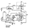
- FIG. 1 is a configuration diagram of a single-phase bridge circuit according to a first embodiment of the present invention.
- FIG. 5 is a diagram illustrating an operation when the upper arm is turned on in the single-phase bridge circuit according to the first embodiment of the present invention.
- FIG. 4 is a diagram illustrating an operation when the upper arm is turned off in the single-phase bridge circuit according to the first embodiment of the present invention. It is a figure showing a single phase bridge circuit of a 2nd embodiment of the present invention. It is a figure showing a single phase bridge circuit of a 3rd embodiment of the present invention. It is a figure showing a single phase bridge circuit of a 4th embodiment of the present invention. It is a figure showing the single phase bridge circuit of a 5th embodiment of the present invention.
- FIG. 1 is a diagram illustrating an example of a circuit configuration of a power conversion device to which the present invention has been applied.
- FIG. 14 is a diagram illustrating a layout (top view) in which the circuit of the power conversion device in FIG. 13 is mounted on a substrate.
- FIG. 15 is a diagram illustrating an example of a wiring layout (L1 layer) in the circuit configuration illustrated in FIG. 14.
- FIG. 15 is a diagram illustrating an example of a wiring layout (L2 layer) in the circuit configuration illustrated in FIG. 14.
- FIG. 15 is a diagram illustrating an example of a wiring layout (L3 layer) in the circuit configuration illustrated in FIG. 14.
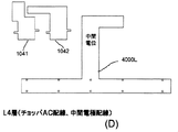
- FIG. 15 is a diagram illustrating an example of a wiring layout (L4 layer) in the circuit configuration illustrated in FIG. 14.
- FIG. 15B is a sectional view taken along the line B-B ′ of FIG. 15A.
- an uninterruptible power converter will be described as an example of a power converter having a plurality of operating states.
- the purpose of the present embodiment partially overlaps with the above-described object, for example, a high-efficiency and small-sized power conversion device that suppresses gate oscillation due to high-speed driving of a power semiconductor device and reduces power semiconductor device loss is realized. It is to be.
- FIG. 1 is a schematic configuration diagram of a power conversion device 100 to which an embodiment of the present invention is applied.
- the power conversion device 100 includes a converter 102, an inverter 103, a chopper 104, and a higher-level control circuit 105 for controlling these.
- the converter 102 is a three-phase converter that converts three-phase AC power supplied from a commercial power supply (AC power supply) 106 to DC power and supplies the DC power to the inverter 103.
- AC power supply AC power supply
- the inverter 103 is a three-phase inverter that converts the DC power supplied from the converter 102 into three-phase AC power again and supplies it to the load 108.
- the chopper 104 raises or lowers the DC power supplied from the storage battery (DC power supply) 107 to a predetermined voltage, converts the DC power to a predetermined DC power, and supplies the DC power to the inverter 103.
- the host control circuit 105 controls the converter 102, the inverter 103, and the chopper 104.
- the host control circuit 105 is, for example, a microcomputer and includes a processor, a memory, an input / output circuit, and the like.
- the chopper 104 supplies the power stored in the storage battery 107 to the inverter 103 as DC power.
- the inverter 103 converts the DC power supplied from the chopper 104 into AC power and supplies the AC power to the load 108. Thereby, the power converter 100 can supply power to the load 108 without interruption.
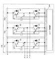
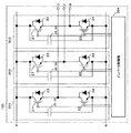
- FIG. 2 is a schematic internal configuration diagram of the converter 102, the inverter 103, and the chopper 104. As shown in FIG. 2, the converter 102, the inverter 103, and the chopper 104 include a plurality of rectifying elements and switching elements.
- FIG. 3 is an equivalent circuit diagram of the internal configuration of the converter 102.
- the converter 102 includes three half-bridge circuits 201, 202, and 203 (power conversion units), and these half-bridge circuits 201, 202, and 203 include a converter control unit (a power conversion unit driving unit). 204.
- the converter 102 converts three-phase AC power supplied from the R, S, and T terminals from the three-phase AC commercial power supply 106 into DC power between the positive terminal P and the negative terminal N.
- the half-bridge circuit 201 includes an upper arm switching element 21 and a rectifying element 23, and a lower arm switching element 22 and a rectifying element 24.
- IGBTs Insulated Gate Bipolar Transistors
- diodes are used for the rectifying elements 23 and 24, but the switching elements 21 and 22 are not limited to these.
- the rectifier 23 is connected in the direction from the emitter to the collector of the switching element 21.
- the emitter of the switching element 21 is connected to the collector of the switching element 22 and the AC terminal R.
- Capacitors 25 and 26 are connected in parallel between the collector of switching element 21 and the emitter of switching element 22. In the circuit diagram of FIG. 3, the parallel connection of the capacitor 25 and the capacitor 26 is omitted and the symbol of a single capacitor is shown for easy viewing of the drawing.
- the gate of the switching element 21 is connected to the converter control unit 204.
- the rectifying element 24 is connected in the direction from the emitter to the collector of the switching element 22.
- the gate of the switching element 22 is connected to the converter control unit 204.
- the half-bridge circuit 202 is configured similarly to the half-bridge circuit 201 (power conversion unit) except that the connection node between the emitter of the switching element 21 and the collector of the switching element 22 is connected to the AC terminal S. .
- the half-bridge circuit 203 is configured similarly to the half-bridge circuit 201 (power conversion unit) except that the connection node between the emitter of the switching element 21 and the collector of the switching element 22 is connected to the AC terminal T. .
- the three-phase AC power supplied from the commercial power supply 106 is supplied to the half-bridge circuits 201, 202, and 203 of each phase of the converter 102 via the AC terminals R, S, and T.
- the switching timing of the upper-arm switching elements 21 and rectifiers 23 and the lower-arm switching elements 22 and rectifiers 24 of the half-bridge circuits 201, 202, and 203 are controlled by a converter control unit 204 to rectify the AC power. I do.
- FIG. 4 is an equivalent circuit diagram showing a configuration of the inverter 103.
- the inverter 103 includes three half-bridge circuits 301, 302, and 303 (power conversion units), and is further controlled by an inverter control unit (power conversion unit driving unit) 304. Inverter 103 converts DC power between the P terminal and the N terminal into three-phase AC power.
- the half-bridge circuit 301 is configured similarly to the half-bridge circuit 201 (see FIG. 3) except that a connection node between the emitter of the switching element 21 and the collector of the switching element 22 is connected to the AC terminal U. .
- the half-bridge circuit 302 is configured similarly to the half-bridge circuit 201 (see FIG. 3) except that a connection node between the emitter of the switching element 21 and the collector of the switching element 22 is connected to the AC terminal V. .
- the half-bridge circuit 303 is configured similarly to the half-bridge circuit 201 (see FIG. 3) except that a connection node between the emitter of the switching element 21 and the collector of the switching element 22 is connected to the AC terminal W. .
- the DC power converted by the converter 102 is supplied between the terminal P and the terminal N.
- the switching timing of the switching element 21 and the rectifying element 23 of the upper arm and the switching element 22 and the rectifying element 24 of the lower arm of the half-bridge circuits 301, 302, 303 are controlled by the inverter control unit 304 so that the DC power is It is converted to AC power and output to AC terminals U, V, W.
- FIG. 5 is an equivalent circuit diagram showing the configuration of the chopper 104.
- the chopper 104 includes a half-bridge circuit 401 (power conversion unit) and a reactor 406, and is controlled by a chopper control unit (power conversion unit driving unit) 405.
- the chopper 104 mutually converts a low DC voltage from the storage battery 107 and a high DC voltage between the terminal P and the terminal N.
- the half-bridge circuit 401 is configured similarly to the half-bridge circuit 201 (see FIG. 3) except that the connection node between the emitter of the switching element 21 and the collector of the switching element 22 is connected to the terminal C.
- Reactor 406 connects the positive electrode of storage battery 107 and terminal C.
- the converter 102, the inverter 103, and the chopper 104 mounted on the power conversion device 100 to which the embodiment of the present invention is applied are each composed of the upper-arm switching element 21 and the rectifier element 23 and the lower-arm switching element.
- a two-level half-bridge circuit 20 in which a rectifying element 22 and a rectifying element 24 are connected in series has a basic configuration.
- the power device 30 is composed of IGBTs (switching elements 21 and 22) and diodes (rectifiers 23 and 24), but is not limited thereto, and is not limited thereto.
- SiC-MOSFET Metal-Oxide-Semiconductor @ Field-
- Other power devices such as Effect @ Transistor may be used.
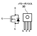
- FIG. 6 (6A, 6B) shows the power device 30 (the switching element and the rectifying element (21 and 23, 22 and 24) in the half bridge circuits 201 to 203, 301 to 303, and 401) according to the embodiment of the present invention.
- FIG. 3 is a diagram illustrating an appearance of a cooling fin 40 connected to a power device 30.
- the power device 30 in FIG. 6A is, for example, a SiC-MOSFET and has a form in which a switching element and a diode are included in one package.
- FIG. 6A shows the appearance of the power device 30, and FIG. 6B shows the appearance of the power device 30 with the cooling fins 40 connected thereto.
- FIG. 7A shows a single-phase bridge circuit according to the first embodiment of the present invention.
- the single-phase bridge circuit of FIG. 7A includes two power semiconductor elements and a separate gate drive circuit.
- the single-phase bridge circuit (bridge circuit) includes an upper arm device 30H (first power device) and a lower arm device 30L (second power device) connected in series thereto.
- the individual gate drive circuits 50H and 50L each include a clamp SW (SWc) for connecting the gate and the source when the gate is off, a clamp SW control circuit, and a clamp resistor circuit (Rc) in series with the clamp SW.
- the clamp SW means a switch for clamping (switching element).
- GDS in FIG. 7A indicates a gate drive signal (gate signal).
- the gate drive circuit 50L charges and discharges the capacitance of the gate of the lower arm device 30L (second power device).
- the clamp switch SWc (switching element) and the clamp resistor circuit Rc (first resistor) form a clamp circuit.
- the clamp circuit conducts between the gate of the lower arm device 30L and the source of the lower arm device 30L.
- the clamp switch SWc (switching element) is a bidirectional switching element capable of flowing a current bidirectionally in an ON state. Thereby, the gate voltage oscillation can be suppressed in both directions.
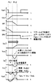
- FIG. 7B ⁇ Operation of the single-phase bridge circuit of FIG. 7A when the upper arm is turned on is shown in FIG. 7B.
- the upper arm turns on Ph.
- the gate signal VgsH of the upper arm is in the Hi state
- the gate signal VgsL of the lower arm is in the Low state.
- the clamp SW control signal SWc of the lower arm is in the Hi state
- the gate-source of the lower arm is conductive through the clamp SW and the clamp resistor circuit.
- the gate current IgL of the lower arm flows in the direction of discharging Cgs. If this gate current is bypassed by the low impedance line of the clamp SW to which the clamp resistance circuit is not connected, the clamp line voltage VcL does not change. As a result, the lower arm gate-source voltage VgsL (VcLV ⁇ VssL) becomes Oscillates to the negative side due to the voltage VssL across the common source inductance. When the negative peak voltage of the gate-source voltage exceeds the negative rating of the gate, the gate oxide film is deteriorated and the life is shortened.
- FIG. 7B shows the operation for two periods.
- FIG. 8 shows a first embodiment of the present invention, similar to FIG. 7 (7A, 7B).
- Each of the individual gate drive circuits comprises a clamp SW (SWc) for connecting between a gate and a source when off, and a clamp SW (SWc).
- An SW control circuit and a clamp resistance circuit (Rc) in series with the clamp SW are included.
- the upper arm turns off Ph.
- the gate signal VgsH of the upper arm is in a low state
- the gate signal VgsL of the lower arm is in a low state.
- the clamp SW control signal SWc of the lower arm is in the Hi state
- the gate-source of the lower arm is conductive through the clamp SW and the clamp resistor circuit.
- the gate oscillation caused by the mirror current increases, while the gate oscillation caused by the common source inductance can be reduced.
- the first embodiment of the present invention it is possible to reduce the gate voltage oscillation of the non-drive arm caused by the common source inductance in the turn-on and turn-off operations. That is, according to the present embodiment, it is possible to suppress the gate voltage oscillation accompanying the high-speed driving of the power device.
- FIG. 9 shows a single-phase bridge circuit according to the second embodiment of the present invention.
- the single-phase bridge circuit of FIG. 9 includes two power semiconductor elements and a separate gate drive circuit.
- the individual gate drive circuit includes a clamp SW (SWc) for connecting between the gate and the source when turned off, a clamp SW control circuit, a clamp resistance circuit (Rc) in series with the clamp SW, and a parallel connection with the clamp resistance circuit. Includes diode Dc.
- the clamp circuit further includes a diode Dc (first diode) connected in parallel to the clamp resistance circuit Rc (first resistor).
- the cathode of the diode Dc (first diode) is connected to the gate of the lower arm device 30L (second power device).
- the clamp switch SWc is turned on.
- the mirror current (Ph1 period in FIG. 8) due to the VdsL fluctuation and the gate current (Ph2 period in FIG. 8) due to the common source inductance voltage fluctuation VssL due to the IsL fluctuation pass through the clamp diode Dc. Through this, the signal is bypassed to the source by the clamp switch SWc. Therefore, even at the time of turn-off, negative gate vibration is reduced.
- the gate oscillation on the negative side can be reduced for both turn-on and turn-off. Therefore, it is particularly effective when the gate negative breakdown voltage of the power semiconductor device is small.
- the load on the gate oxide film can be reduced, and the length of the power semiconductor device can be reduced. It has the effect of extending the life.
- FIG. 10 shows a single-phase bridge circuit according to the third embodiment of the present invention.
- the single-phase bridge circuit of FIG. 10 includes two power semiconductor devices and a separate gate drive circuit.
- the individual gate drive circuit includes a clamp SW (SWc) for connecting between the gate and the source when turned off, a clamp SW control circuit, a clamp resistance circuit (Rc) in series with the clamp SW, and a parallel connection with the clamp resistance circuit. Includes diode Dc.
- the anode of the diode Dc (first diode) is connected to the gate of the lower arm device 30L (second power device).
- the clamp switch SWc is turned on.
- the mirror current (Ph1 period in FIG. 8) due to the VdsL fluctuation and the gate current (Ph2 period in FIG. 8) due to the common source inductance voltage fluctuation VssL due to the IsL fluctuation are caused by the clamp resistor Rc.
- the signal is bypassed to the source by the clamp switch SWc. Therefore, the gate vibration on the positive side is reduced even at the time of turn-off.
- the gate vibration on the positive side can be reduced for both turn-on and turn-off. Therefore, it is particularly effective when the threshold voltage of the power semiconductor device is low, and by suppressing the positive side gate vibration in the non-drive arm, the short-circuit current caused by the simultaneous turning on of the upper and lower arms causes Element destruction can be prevented.
- FIG. 11 shows a single-phase bridge circuit according to a fourth embodiment of the present invention.
- the single-phase bridge circuit of FIG. 11 includes two power semiconductor devices and a separate gate drive circuit.
- the individual gate drive circuit includes a clamp SW (SWc) that connects between the gate and the source when turned off, a clamp SW control circuit, a clamp resistor circuit (Rc1, Rc2) in series with the clamp SW, and the clamp resistor circuit. Includes series clamp diodes (Dc1, Dc2).
- the clamp circuit includes a clamp diode Dc1 (first diode) connected in series to a clamp resistor circuit Rc1 (first resistor), and a clamp resistor circuit Rc2 (second circuit) connected in series to a clamp switch SWc (switching element). And a clamp diode Dc2 (second diode) connected in series to the clamp resistor circuit Rc2.
- the anode of the clamp diode Dc1 is connected to the gate of the lower arm device 30L
- the cathode of the clamp diode Dc2 is connected to the gate of the lower arm device 30L.
- the clamp line voltage VcL can be individually adjusted by turning on and turning off.
- the gate oscillation caused by the common source inductance can be individually reduced according to the switching speed at the time of turn-off and at the time of turn-on.
- FIG. 12 shows a single-phase bridge circuit according to a fifth embodiment of the present invention.
- the single-phase bridge circuit of FIG. 12 includes two power semiconductor devices and a separate gate drive circuit.
- the individual gate drive circuit includes a clamp SW (SWc) that connects between the gate and the source when off, a gate capacitance charge current adjustment resistor Rgon when turned on, a gate capacitance discharge current adjustment resistor Rgoff when turned off, and a gate drive circuit. Circuit BUF.
- the wiring inductance Lp2 from the power semiconductor device to the clamp circuit is mounted so as to be smaller than the wiring inductance Lp1 from the power semiconductor device to the gate drive circuit.
- the inductance Lp2 of the clamp circuit wiring indicating the wiring connecting the gate of the lower arm device 30L (second power device) and the clamp circuit is equal to that of the lower arm device 30L (second power device). It is smaller than the inductance Lp1 of the drive circuit wiring indicating the wiring connecting the gate and the gate drive circuit.
- FIG. 13 is a diagram illustrating an example of a circuit configuration of a power conversion device (power converter) to which the present invention has been applied.
- the DC link capacitor of FIG. 2 is composed of two capacitors 601 and 602 connected in series with each other.
- the connection point between 601 and 602 is connected to the R, S, and T terminals via a capacitor 2100 (first AC filter capacitor) connected to the AC power supply side, and the output side of the inverter 103 (load 108 Side) via a capacitor 2000 (second AC filter capacitor) connected to the U, V, and W terminals.
- connection point between the capacitors 601 and 602 is connected to the capacitor 2000 and the capacitor 2100, and has an intermediate potential 4000.
- Reactor 406A is connected to a connection midpoint (connection point) between upper arm switching element 104-1B and lower arm switching element 104-2B of chopper 104, and upper arm switching element 104-1A and lower arm switching element 104- are connected.
- Reactor 406B is connected to the midpoint of connection with 2A.
- FIG. 14 is a diagram showing a layout (top view) in which the circuit of the power conversion device of FIG. 13 is mounted on a substrate.
- a DC link condenser 600 is arranged upstream (upwind) of the cooling air from the converter 102 and the inverter 103, and a DCAC reactor 800 is arranged downstream (downwind) of the chopper 104.
- the DC link capacitor 600 is disposed on the upstream side of the cooling air of the converter 102 and the inverter 103, the influence of the heat generated by the operation of the converter 102 and the inverter 103 on the DC link capacitor 600 (the influence of the tilt heat) is reduced. Can be removed. Further, since the converter and the chopper do not generate the maximum heat at the same time, the tilt heat between the two can be reduced.
- the DCAC reactor 800 is arranged downstream of the cooling air of the converter 102, the inverter 103 and the chopper 104, the influence of the heat generated by the DCAC reactor 800 on the converter 102, the inverter 103 and the chopper 104 (the influence of the tilting heat) is eliminated. be able to.
- Gate drive circuits 102U1D, 102U2D, 102V1D, 102V2D, 102W1D, and 102W2D (converter control units (power conversion unit drive units) 204) that drive the power devices 30 of the converters 102U, 102V, and 102W are located near the respective power devices 30. Deploy.
- the converter 102 has two sets of the power device 30 and the cooling fin 40 for each of the U phase, the V phase, and the W phase, but the U phase and the V phase are arranged at positions adjacent to each other.
- the respective power devices 30 are arranged to face each other, and the gate drive circuits 102U2D and 102V1D are arranged to face each other.
- a set of the power device 30 and the cooling fin 40 in which the V phase and the W phase are arranged at positions adjacent to each other is such that the respective power devices 30 are arranged to face each other and the gate drive circuits 102V2D and 102W1D Are arranged to face each other.
- the gate drive circuits 103U1D, 103U2D, 103V1D, 103V2D, 103W1D, and 103W2D (the inverter control unit (power conversion unit drive unit) 304) that drive the power devices 30 of the inverters 103U, 103V, and 103W are connected to the respective power devices 30. Place it near.
- the inverter 103 has two sets each including the power device 30 and the cooling fin 40 for each of the U phase, the V phase, and the W phase, but the U phase and the V phase are arranged at positions adjacent to each other.
- the respective power devices 30 are arranged to face each other, and the gate drive circuits 103U2D and 103V1D are arranged to face each other.
- the set of the power device 30 and the cooling fin 40 in which the V phase and the W phase are arranged at positions adjacent to each other is such that the respective power devices 30 are arranged to face each other and the gate drive circuits 103V2D and 103W1D Are arranged to face each other.
- the W phase of the converter 102 and the U phase of the inverter 103 are arranged adjacent to each other, and a set of the power device 30 and the cooling fin 40 arranged at positions adjacent to each other is such that the respective power devices 30 Gate drive circuits 102W2D and 103U1D are arranged to face each other.
- the gate drive circuits 104-1D1, 104-1D2, 104-2D1, and 104-2D2 (chopper control unit (power conversion unit drive unit) 405) for driving the power devices 30 of the choppers 104-1 and 104-2 are provided. It is arranged near each power device 30.
- the chopper 104 has a set of the power device 30 and the cooling fins 40, and each of the choppers 104-1 and 104-2 has two sets.
- the pair of the power device 30 and the cooling fin 40 in which the choppers 104-1 and 104-2 are arranged adjacent to each other is such that the respective power devices 30 are arranged to face each other and the gate drive circuit 104- 1D2 and 104-2D1 are arranged to face each other.
- the power device 30 and its gate drive circuits (102U1D to 102W1D, 103U1D to 103W2D, 104-1D1 to 104-2D2) are arranged close to each other, the wiring inductance of the gate drive circuit is reduced and unnecessary. The resonance can be suppressed, and the power device 30 can be driven at high speed.
- FIG. 15 is a diagram showing an example of a wiring layout in the circuit configuration shown in FIG.
- the wiring example shown in FIG. 15 includes the L1 layer (AC wiring of the converter 102 and the inverter 103), the L2 layer (P wiring), the L3 layer (N wiring), and the L4 layer (AC wiring of the chopper 104, intermediate wiring). (Intermediate electrode wiring with a potential of 4000).
- the power conversion device 100 includes a multilayer substrate including at least a first layer, a second layer, and a third layer in order from the surface.
- the wirings 1021, 1022, and 1023 of the converter 102 are formed in the L1 layer. Further, AC wirings 1031, 1032 and 1033 of the inverter 103 are formed.
- the AC wirings (1031, 1032, 1033) indicating the wirings connected to the AC terminals (U, V, W) of the power converter 100 are arranged in the L1 layer (first layer). Thereby, the cooling efficiency of the AC wiring can be improved.
- the P2 wiring 3000P is formed in the L2 layer. That is, P-pole wiring 3000P indicating a wiring connected to the DC positive terminal (P) of power conversion device 100 is arranged in one of L2 layer (second layer) and L3 layer (third layer).
- the N3 layer has an N-pole wiring 2000N formed thereon. That is, N-pole wiring 2000N indicating a wiring connected to the DC negative terminal (N) of power conversion device 100 is arranged on the other of the L2 layer (second layer) and the L3 layer (third layer).
- FIG. 16 is a cross-sectional view (schematic view) taken along the line B-B ′ of FIG. 15A.
- the gate drive wiring 5000GL4 and the AC intermediate potential wiring 5000ML4 are formed in the L4 layer, and the gate drive wiring 5000GL3 and the N pole wiring 5000ML3 are formed in the L3 layer.
- a gate drive wiring 5000GL2 and a P-pole wiring 5000ML2 are formed, and in the L1 layer, a gate drive wiring 5000GL1 and an AC wiring 5000ML1 are formed.
- An insulating layer 5000I is arranged between the layers to insulate each other. Further, a via 6200 is formed through the L1 layer to the L4 layer, and a lead 6100 is arranged in the via 6200. Above the L1 layer, a lower arm device 30L and an upper arm device 30H connected to the lead 6100 are connected. A gate drive circuit and a gate clamp circuit (clamp circuit) are arranged above the gate drive wiring 5000GL1 in the L1 layer.
- the gate drive wiring 5000G and the main circuit wiring 5000M can be separated in the layer direction to reduce noise.
- the main circuit wiring 5000M has a multilayer wiring structure (laminate wiring structure), the inductance can be reduced, and the jump of the main circuit voltage accompanying the switching operation can be suppressed.
- the source lead of the power device and the source wiring of the gate drive circuit are connected in the L1 layer.
- a gate source line indicating a line connecting the gate drive circuit 50L and the source of the lower arm device 30L (second power device) is arranged in the L1 layer (first layer).
- the source wiring of the gate drive circuit is wired by Lp1
- the gate wiring of the gate drive circuit is wired by Lp2
- both have a laminated structure, thereby reducing the wiring inductance of the gate drive circuit. Gate vibration in the non-drive arm can be reduced.
- the present invention is not limited to the above-described embodiment, and includes various modifications.
- the above-described embodiments have been described in detail for easy understanding of the present invention, and are not necessarily limited to those having all the described configurations.
- a part of the configuration of one embodiment can be replaced with the configuration of another embodiment, and the configuration of one embodiment can be added to the configuration of another embodiment.
- AC power supply 107: Storage battery (DC power supply) 108 Load 201 Half bridge circuit 202 Half bridge circuit 203 Half bridge circuit 204 Converter control unit (power conversion unit drive unit) 301 half bridge circuit 302 half bridge circuit 303 half bridge circuit 304 inverter control unit (power conversion unit drive unit) 401: half bridge circuit 405: chopper control unit (power conversion unit drive unit) 406 reactor 406A reactor 406B reactor 600 link capacitor 601 capacitor 602 capacitor 800 ... reactor 2000 ... capacitor 2100 ... capacitor 5000I ... insulating layer 6100 ... lead 6200 ... via
Landscapes
- Engineering & Computer Science (AREA)
- Power Engineering (AREA)
- Inverter Devices (AREA)
- Power Conversion In General (AREA)
- Electronic Switches (AREA)
Abstract
Dans la présente invention, un circuit en pont monophasé (circuit en pont) comprend un dispositif de bras supérieur (30H) (premier dispositif d'alimentation) et un dispositif de bras inférieur (30L) (second dispositif d'alimentation) qui est connecté en série à ce dernier. Un circuit de commande de grille (50L) charge et décharge la capacité d'une grille du dispositif de bras inférieur (30L) (second dispositif d'alimentation). Un circuit de calage permet la conduction entre la grille du dispositif de bras inférieur (30L) et une source du dispositif de bras inférieur (30L) (second dispositif d'alimentation) si une tension (VgsL) entre la grille et la source du dispositif de bras inférieur (30L) est inférieure à une valeur prescrite (Vthc). Le circuit de calage comprend un commutateur de calage (SWc) (élément de commutation) et un circuit de résistance de calage (Rc) (première résistance).
Applications Claiming Priority (2)
| Application Number | Priority Date | Filing Date | Title |
|---|---|---|---|
| JP2018-123032 | 2018-06-28 | ||
| JP2018123032A JP7011544B2 (ja) | 2018-06-28 | 2018-06-28 | 電力変換装置 |
Publications (1)
| Publication Number | Publication Date |
|---|---|
| WO2020003634A1 true WO2020003634A1 (fr) | 2020-01-02 |
Family
ID=68986937
Family Applications (1)
| Application Number | Title | Priority Date | Filing Date |
|---|---|---|---|
| PCT/JP2019/010388 Ceased WO2020003634A1 (fr) | 2018-06-28 | 2019-03-13 | Dispositif de conversion de courant |
Country Status (2)
| Country | Link |
|---|---|
| JP (1) | JP7011544B2 (fr) |
| WO (1) | WO2020003634A1 (fr) |
Cited By (3)
| Publication number | Priority date | Publication date | Assignee | Title |
|---|---|---|---|---|
| WO2021143450A1 (fr) * | 2020-01-14 | 2021-07-22 | 北京集创北方科技股份有限公司 | Circuit de commande de commutateur, circuit commutateur de multiplexeur et procédé de commande pour circuit de commande de commutateur de multiplexeur |
| WO2023037635A1 (fr) * | 2021-09-13 | 2023-03-16 | オムロン株式会社 | Circuit de commutation et convertisseur de puissance |
| WO2025084402A1 (fr) * | 2023-10-20 | 2025-04-24 | 株式会社日立製作所 | Dispositif de conversion d'énergie électrique |
Citations (2)
| Publication number | Priority date | Publication date | Assignee | Title |
|---|---|---|---|---|
| JP2013013051A (ja) * | 2011-06-01 | 2013-01-17 | Denso Corp | パワーmosfetの駆動回路およびその素子値決定方法 |
| JP2014075694A (ja) * | 2012-10-04 | 2014-04-24 | Renesas Electronics Corp | ゲートドライバ、及びスイッチング方法 |
-
2018
- 2018-06-28 JP JP2018123032A patent/JP7011544B2/ja active Active
-
2019
- 2019-03-13 WO PCT/JP2019/010388 patent/WO2020003634A1/fr not_active Ceased
Patent Citations (2)
| Publication number | Priority date | Publication date | Assignee | Title |
|---|---|---|---|---|
| JP2013013051A (ja) * | 2011-06-01 | 2013-01-17 | Denso Corp | パワーmosfetの駆動回路およびその素子値決定方法 |
| JP2014075694A (ja) * | 2012-10-04 | 2014-04-24 | Renesas Electronics Corp | ゲートドライバ、及びスイッチング方法 |
Cited By (3)
| Publication number | Priority date | Publication date | Assignee | Title |
|---|---|---|---|---|
| WO2021143450A1 (fr) * | 2020-01-14 | 2021-07-22 | 北京集创北方科技股份有限公司 | Circuit de commande de commutateur, circuit commutateur de multiplexeur et procédé de commande pour circuit de commande de commutateur de multiplexeur |
| WO2023037635A1 (fr) * | 2021-09-13 | 2023-03-16 | オムロン株式会社 | Circuit de commutation et convertisseur de puissance |
| WO2025084402A1 (fr) * | 2023-10-20 | 2025-04-24 | 株式会社日立製作所 | Dispositif de conversion d'énergie électrique |
Also Published As
| Publication number | Publication date |
|---|---|
| JP7011544B2 (ja) | 2022-02-10 |
| JP2020005411A (ja) | 2020-01-09 |
Similar Documents
| Publication | Publication Date | Title |
|---|---|---|
| US10715053B2 (en) | Power conversion apparatus in which an inductance of a last off closed circuit is smaller than an inductance of a non-last off closed circuit | |
| JP3598933B2 (ja) | 電力変換装置 | |
| JPH03107328A (ja) | 電力変換装置のスナバ回路 | |
| US20110013438A1 (en) | inverter topologies usable with reactive power | |
| CN113394955B (zh) | 半导体装置的布线电路及其控制方法、半导体装置、电力变换装置、铁路车辆用电气系统 | |
| CN1518791A (zh) | 电子功率电路 | |
| US12003188B2 (en) | Modular parallel half-bridge integrated assembly with annular layout | |
| US11863166B2 (en) | Power semiconductor module and power converter | |
| JPH11234104A (ja) | 半導体モジュール及びインバータ装置 | |
| JP2019017112A (ja) | パワー回路 | |
| WO2020003634A1 (fr) | Dispositif de conversion de courant | |
| US20170117820A1 (en) | Semiconductor device | |
| JP2957407B2 (ja) | 3レベルインバータ装置 | |
| JP7655399B2 (ja) | 半導体装置 | |
| JP5571013B2 (ja) | 半導体スイッチ、及び電力変換装置 | |
| JP7132099B2 (ja) | 電力変換装置 | |
| JP2017042040A (ja) | 電力変換装置 | |
| JP7276006B2 (ja) | スナバ回路および電力変換装置 | |
| JP2004274801A (ja) | インバータ回路 | |
| JPH07231669A (ja) | 高周波インバータ装置 | |
| JP4156258B2 (ja) | 共振型インバータ | |
| JPH01209951A (ja) | 電力変換装置 | |
| CN119631289A (zh) | 半导体装置以及电力变换装置 | |
| JP7547738B2 (ja) | スナバ回路および電力変換装置 | |
| JP4487682B2 (ja) | コンデンサとその設置方法 |
Legal Events
| Date | Code | Title | Description |
|---|---|---|---|
| 121 | Ep: the epo has been informed by wipo that ep was designated in this application |
Ref document number: 19826369 Country of ref document: EP Kind code of ref document: A1 |
|
| NENP | Non-entry into the national phase |
Ref country code: DE |
|
| 122 | Ep: pct application non-entry in european phase |
Ref document number: 19826369 Country of ref document: EP Kind code of ref document: A1 |