WO2020003675A1 - Dispositif d'analyse par fluorescence de rayons x à réflexion totale et procédé de mesure - Google Patents
Dispositif d'analyse par fluorescence de rayons x à réflexion totale et procédé de mesure Download PDFInfo
- Publication number
- WO2020003675A1 WO2020003675A1 PCT/JP2019/014524 JP2019014524W WO2020003675A1 WO 2020003675 A1 WO2020003675 A1 WO 2020003675A1 JP 2019014524 W JP2019014524 W JP 2019014524W WO 2020003675 A1 WO2020003675 A1 WO 2020003675A1
- Authority
- WO
- WIPO (PCT)
- Prior art keywords
- total reflection
- measurement sample
- ray
- fluorescent
- differential curve
- Prior art date
- Legal status (The legal status is an assumption and is not a legal conclusion. Google has not performed a legal analysis and makes no representation as to the accuracy of the status listed.)
- Ceased
Links
Images




Classifications
-
- G—PHYSICS
- G01—MEASURING; TESTING
- G01B—MEASURING LENGTH, THICKNESS OR SIMILAR LINEAR DIMENSIONS; MEASURING ANGLES; MEASURING AREAS; MEASURING IRREGULARITIES OF SURFACES OR CONTOURS
- G01B15/00—Measuring arrangements characterised by the use of electromagnetic waves or particle radiation, e.g. by the use of microwaves, X-rays, gamma rays or electrons
- G01B15/02—Measuring arrangements characterised by the use of electromagnetic waves or particle radiation, e.g. by the use of microwaves, X-rays, gamma rays or electrons for measuring thickness
-
- G—PHYSICS
- G01—MEASURING; TESTING
- G01N—INVESTIGATING OR ANALYSING MATERIALS BY DETERMINING THEIR CHEMICAL OR PHYSICAL PROPERTIES
- G01N23/00—Investigating or analysing materials by the use of wave or particle radiation, e.g. X-rays or neutrons, not covered by groups G01N3/00 – G01N17/00, G01N21/00 or G01N22/00
- G01N23/20—Investigating or analysing materials by the use of wave or particle radiation, e.g. X-rays or neutrons, not covered by groups G01N3/00 – G01N17/00, G01N21/00 or G01N22/00 by using diffraction of the radiation by the materials, e.g. for investigating crystal structure; by using scattering of the radiation by the materials, e.g. for investigating non-crystalline materials; by using reflection of the radiation by the materials
-
- G—PHYSICS
- G01—MEASURING; TESTING
- G01N—INVESTIGATING OR ANALYSING MATERIALS BY DETERMINING THEIR CHEMICAL OR PHYSICAL PROPERTIES
- G01N23/00—Investigating or analysing materials by the use of wave or particle radiation, e.g. X-rays or neutrons, not covered by groups G01N3/00 – G01N17/00, G01N21/00 or G01N22/00
- G01N23/22—Investigating or analysing materials by the use of wave or particle radiation, e.g. X-rays or neutrons, not covered by groups G01N3/00 – G01N17/00, G01N21/00 or G01N22/00 by measuring secondary emission from the material
- G01N23/223—Investigating or analysing materials by the use of wave or particle radiation, e.g. X-rays or neutrons, not covered by groups G01N3/00 – G01N17/00, G01N21/00 or G01N22/00 by measuring secondary emission from the material by irradiating the sample with X-rays or gamma-rays and by measuring X-ray fluorescence
Definitions
- the present invention relates to a total reflection X-ray fluorescence spectrometer and a measuring method.
- a parameter called a film thickness is mainly managed.
- the film thickness has been measured using a fluorescent X-ray analysis method or an X-ray reflectivity method (XRR: X-Ray Reflectometry).
- XRR X-Ray Reflectometry
- the fluorescent X-ray analysis method is based on the adhesion amount (mass per unit area) obtained from the measured intensity of the fluorescent X-ray, and the density obtained from the literature value or another method (for example, X-ray reflectivity method). (See Patent Document 1 below).
- the X-ray reflectivity method is a method of irradiating a measurement sample with primary X-rays in the vicinity of a critical angle of total reflection and calculating surface roughness, density, film thickness, etc. based on attenuation due to interference of reflected X-rays. (See Patent Document 2 below).
- the attached amount is divided by the density.
- the density is information obtained by literature or other methods, and is not the density obtained from an actual measurement sample. Therefore, the calculated film thickness includes an error. Further, in the X-ray reflectivity method, there is a limitation on a range of a measured film thickness.
- the present invention has been made in view of the above problems, and an object of the present invention is to provide a method for measuring the density and thickness of a measurement sample and a total reflection X-ray fluorescence analyzer for measuring the density and thickness of the measurement sample. That is, it can be realized easily at low cost.
- a detector that measures the intensity of the fluorescent X-rays generated from the measurement sample, and obtains a differential curve by differentiating the relationship between the intensity of the fluorescent X-rays and the incident angle with respect to the incident angle.
- a calculating unit that obtains the critical angle for total reflection from a differential curve, and further calculates the density and / or film thickness of the measurement sample based on the critical angle for total reflection and the wavelength of the primary X-ray. It is characterized by.
- the total reflection X-ray fluorescence spectrometer according to claim 2 is the total reflection X-ray fluorescence spectrometer according to claim 1, wherein the calculation unit acquires a peak angle of the differential curve as the critical angle for total reflection. It is characterized.
- the total reflection X-ray fluorescence spectrometer according to claim 3 is the total reflection X-ray fluorescence spectrometer according to claim 1 or 2, wherein the calculation unit further includes: The method is characterized in that the amount of adhesion of the measurement sample is quantitatively analyzed, and the film thickness of the measurement sample is calculated based on the amount of adhesion and the density.
- the total reflection X-ray fluorescence spectrometer according to claim 4 is the total reflection X-ray fluorescence spectrometer according to any one of claims 1 to 3, wherein the arithmetic unit is configured to perform the calculation based on a shape of the differential curve. It is characterized in that the surface roughness of the measurement sample is calculated.
- the surface roughness of the measurement sample is calculated based on a relationship between a peak width of the curve and the surface roughness and a peak width of the differential curve acquired based on the measurement sample.
- the density and the thickness of the measurement sample can be measured easily at low cost.
- FIG. 1 is a diagram schematically illustrating a total reflection X-ray fluorescence spectrometer according to an embodiment of the present invention. It is a flowchart which shows the measuring method of a density. It is a figure showing an example showing the relation between incident angle and intensity of fluorescent X-rays. It is a figure showing an example of a differential curve. It is a figure showing another example of a differential curve. It is a figure showing another example of a differential curve. 5 is a flowchart illustrating a method for measuring a film thickness. It is a flowchart which shows the measuring method of surface roughness. 6 is a flowchart illustrating a method of measuring a correction value.
- FIG. 1 is a view schematically showing a total reflection X-ray fluorescence spectrometer 100.
- the total reflection X-ray fluorescence spectrometer 100 includes a sample stage 102, an X-ray source 104, a detector 106, a counter 108, and a calculation unit 110.
- a measurement sample 112 is arranged on the sample stage 102.
- the measurement sample 112 is, for example, a silicon substrate on which a thin film of silicon oxide (SiO2) is formed.
- the X-ray source 104 irradiates monochromatic primary X-rays 114 while changing the incident angle with respect to the surface of the measurement sample 112 over the critical angle of total reflection of the measurement sample 112. Specifically, for example, the X-ray source 104 converts the X-rays emitted from an X-ray tube (not shown) into a single color using a monochromator (not shown) such as a spectral crystal and the like, and a slit (not shown). Squeeze thinly.
- the X-ray source 104 irradiates the monochromatic primary X-ray 114 onto the surface of the measurement sample 112 within an angle range of 0.3 degrees before and after the critical angle for total reflection (for the sake of explanation, actual irradiation is performed). Angle greater than the angle).
- the critical angle for total reflection is an angle unique to the measurement sample 112.
- the angle range is set in a range in which a total reflection critical angle can be obtained from a differential curve described later.
- the fluorescent X-ray 116 is generated from the measurement sample 112 irradiated with the primary X-ray 114.
- the detector 106 measures the intensity of the fluorescent X-ray 116 generated from the measurement sample 112.
- the detector 106 is a semiconductor detector such as an SDD detector.
- the detector 106 measures the intensity of the fluorescent X-ray 116 and outputs a pulse signal having a peak value corresponding to the measured energy of the fluorescent X-ray 116.
- the detector 106 measures the intensity of the fluorescent X-ray 116 each time the X-ray source 104 changes the incident angle of the fluorescent X-ray 116 on the measurement sample 112.
- Counter 108 counts the pulse signal output as the measured intensity of detector 106 according to the peak value.
- the counter 108 is a multi-channel analyzer, and counts the output pulse signal of the detector 106 for each channel corresponding to the energy of the fluorescent X-ray 116, and calculates the intensity of the fluorescent X-ray 116. Output to the arithmetic unit 110.
- the calculation unit 110 calculates the density and / or the film thickness. A specific process performed by the arithmetic unit 110 will be described with reference to a flowchart (FIG. 2) illustrating a density measuring method according to the present invention.
- the measurement sample 112 is placed on the sample table 102 (S202).
- the measurement sample 112 is a silicon substrate (bare silicon) or a silicon substrate having a thin film of silicon carbide (SiC) or silicon oxide (SiO2) formed on the surface.
- the measurement sample 112 is placed on the sample stage 102 and irradiated with primary X-rays 114 from the X-ray source 104.
- the measurement sample 112 irradiated with the primary X-ray 114 generates a fluorescent X-ray 116.
- the arithmetic unit 110 acquires the intensity of the fluorescent X-ray 116 counted by the counter 108 (S204). Specifically, the arithmetic unit 110 acquires the intensity of the fluorescent X-ray 116 counted by the counter 108 for each incident angle of the primary X-ray 114 on the measurement sample 112.
- FIG. 3 is an example showing a relationship between the incident angle and the intensity of the fluorescent X-ray 116 (Si-k ⁇ ray) of Si which is a constituent element of the substrate. As shown in FIG. 3, as the incident angle increases, the intensity of the fluorescent X-ray 116 rapidly increases at a specific angle as a boundary. Further, the relationship between the incident angle and the intensity of the fluorescent X-ray 116 has an inflection point. The gradient of the intensity of the fluorescent X-ray 116 becomes gradually gentler at an angle larger than the inflection point.
- the change in the intensity of the fluorescent X-rays 116 is caused by the following phenomenon.
- the incident angle is smaller than the critical angle for total reflection, the primary X-ray 114 does not enter the inside of the measurement sample 112 due to the total reflection on the surface of the measurement sample 112. Therefore, the fluorescent X-ray 116 generated at the incident angle is very small.
- the incident angle becomes larger than the critical angle for total reflection, the primary X-ray 114 enters the inside of the measurement sample 112.
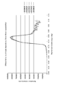
- the calculation unit 110 obtains a differential curve by differentiating the relationship between the intensity of the fluorescent X-rays 116 and the incident angle with respect to the incident angle (S206). Specifically, the arithmetic unit 110 differentiates the relationship between the intensity of the fluorescent X-rays 116 (Si-k ⁇ rays) acquired in S204 and the incident angle with respect to the incident angle, as shown in FIG. Get the curve. Since the relationship between the incident angle and the intensity of the fluorescent X-ray 116 shown in FIG. 3 has an inflection point, the differential curve shown in FIG. 4 has a peak. This inflection point, that is, the peak of the differential curve is the critical angle. The horizontal axis in FIG.
- FIG. 4 is an incident angle based on a mechanical origin on design before performing correction described later.
- FIG. 4 is a diagram showing a measurement result for correcting the incident angle and confirming the reproducibility, and showing a differential curve measured using a silicon substrate having a known total reflection critical angle as a standard sample.
- FIG. 4 shows five measurement results for the same measurement sample 112.
- the peak angle of the differential curve is acquired by performing, for example, smoothing by weighted moving average or function fitting.
- Table 1 is a table showing each value included in FIG.
- FIG. 5 is a diagram showing differential curves obtained based on the intensity of the fluorescent X-ray 116 (Si-k ⁇ ray) with respect to the three kinds of measurement samples 112.
- the three kinds of measurement samples 112 are a silicon substrate, a silicon substrate having a silicon carbide (SiC) thin film formed on its surface, and a silicon substrate having a silicon oxide (SiO2) thin film formed on its surface.
- SiC silicon carbide
- SiO2 silicon oxide
- FIG. 6 is a diagram showing differential curves obtained based on five types of measurement samples 112.
- the five kinds of measurement samples 112 are a silicon substrate (Si in FIG. 6), a silicon substrate having a 10 nm thick titanium (Ti) thin film formed on the surface (FIG. 6, Ti (10 nm) in Table 2), and a surface.
- FIG. 6 shows a silicon substrate (Co (6 nm), Co (8 nm), and Co (10 nm) in FIG. 6, Table 2) on which a cobalt (Co) thin film having a thickness of 6 nm, 8 nm, and 10 nm is formed.
- the fluorescent X-rays 116 used for the intensity measurement include a Si-k ⁇ line of a silicon substrate, a Ti-k ⁇ line of a silicon substrate having a titanium thin film formed on its surface, and a Co-ka of a silicon substrate having a cobalt thin film formed on its surface. Line.
- Table 2 shows the densities calculated by the later-described calculations for the five types of measurement samples 112 shown in FIG.
- metals such as Ti and Co formed as an extremely thin film on a silicon substrate are considered to be silicided, and it is considered that a titanium silicide (TiSiX) thin film and a cobalt silicide (CoSiX) thin film are formed.
- TiSiX titanium silicide
- CoSiX cobalt silicide
- the calculation unit 110 acquires a critical angle for total reflection from the differential curve (S208). Specifically, the calculation unit 110 acquires the angle at the peak of the differential curve acquired in S206 as the critical angle for total reflection. For example, the calculation unit 110 acquires a critical angle for total reflection of 0.184 degrees based on the differential curve shown in FIG. Here, the arithmetic unit 110 acquires the critical angle for total reflection by averaging the peak angles acquired from the five differential curves.
- the peak of the differential curve shown in FIG. 4 is located at -0.066 degrees.
- the acquired total reflection critical angle includes an error due to the inclination of the sample stage 102.
- the critical angle for total reflection of 0.184 degrees is a value obtained by correcting an error with respect to the value of -0.066 degrees measured by an actual apparatus. The details of the error correction method will be described later.
- the calculation unit 110 calculates the density of the measurement sample 112 based on the critical angle for total reflection and the wavelength of the primary X-ray 114 (S210). Specifically, the arithmetic unit 110 applies the critical angle of total reflection acquired in S208 and the wavelength of the primary X-ray 114 applied to the measurement sample 112 to Equation 1 representing the relationship between the critical angle of total reflection and the density. Thus, the density of the measurement sample 112 is calculated.
- ⁇ c is the critical angle for total reflection.
- ⁇ is a constant.
- ⁇ is the wavelength of the primary X-ray 114 irradiated on the measurement sample 112.
- Z is an atomic number.
- A is the mass number.
- the atomic number of Ti is 22, the mass number is 48, the atomic number of Co is 27, and the mass number is 59.
- the unknowns included in the right side of Equation 1 are only the density ⁇ (g / cm 3) of the surface of the measurement sample 112 irradiated with the primary X-ray 114.
- the critical angle of total reflection on the left side is calculated in S208. Therefore, according to the present invention, the density of the measurement sample 112 (the density of the film formed on the surface of the measurement sample 112) can be easily obtained.
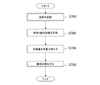
- FIG. 7 is a flowchart showing a method for measuring a film thickness according to the present invention. Note that if the density is obtained by the above method, the method shown in the flowchart of FIG. 7 uses the fluorescent X-ray analyzer that irradiates the measurement sample 112 with the primary X-ray 114 at an angle larger than the total reflection critical angle. May be performed.
- the measurement sample 112 is placed on the sample table 102 (S702).
- the measurement sample 112 is the measurement sample 112 used in S202, and is a silicon substrate having a silicon carbide (SiC) thin film, a silicon oxide (SiO2) thin film, etc. formed on the surface.
- the measurement sample 112 is placed on the sample stage 102, and the X-ray source 104 irradiates the measurement sample 112 with primary X-rays 114 that have been made monochromatic.
- the measurement sample 112 irradiated with the primary X-ray 114 generates a fluorescent X-ray 116.
- the arithmetic unit 110 acquires the intensity of the fluorescent X-ray 116 counted by the counter 108 (S704). Specifically, the calculation unit 110 acquires the intensity of the fluorescent X-ray 116 generated from the analysis element included in the measurement sample 112 whose density has been obtained.
- the arithmetic unit 110 quantitatively analyzes the amount of the measurement sample 112 attached based on the intensity of the fluorescent X-ray 116 (S706). Specifically, for example, using a conventional technique such as a fundamental parameter method or a calibration curve method, the calculation unit 110 determines the amount of the element attached (the mass per unit area) based on the intensity of the fluorescent X-ray 116 obtained in S704. ) Is calculated.
- the calculation unit 110 calculates the film thickness of the analysis element based on the amount of adhesion and the density (S708). Specifically, the calculation unit 110 calculates the film thickness of the measurement sample 112 by applying the density acquired in S210 and the adhesion amount acquired in S706 to Equation 2.
- t (cm) is the film thickness of the measurement sample 112.
- c (g / cm2) is the amount of adhesion.
- ⁇ (g / cm3) is the density.
- the calculation unit 110 can calculate the film thickness from the information on the amount of adhesion and the density.
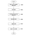
- FIG. 8 is a flowchart showing a method for measuring surface roughness according to the present invention.
- the calculation unit 110 acquires the relationship between the peak width of the differential curve acquired based on the sample whose surface roughness is known and the surface roughness (S802). Specifically, first, the computing unit 110 acquires a differential curve for a sample whose surface roughness is known by the same steps as S202 to S206. As the peak width of the differential curve, for example, the half width of the peak is used. The calculating unit 110 obtains the relationship between the known surface roughness and the half-value width by calculating the half-value width of the differential curve. A calibration curve for calculating surface roughness may be created using a plurality of samples whose surface roughness is known.
- the peak width of the differential curve tends to increase as the surface roughness of the measurement sample 112 increases.
- the intercept of each peak waveform on the vertical axis 0.5 is a half width.
- the half widths of the silicon substrate, the titanium thin film, and the cobalt thin film (three types) are 0.090 °, 0.106 °, and 0.131 °, respectively. Accordingly, the results in FIG. 6 indicate that the surface roughness of the cobalt thin film is the same regardless of the thickness, is larger than the surface roughness of the titanium thin film, and has the smallest surface roughness of the silicon substrate.
- a differential curve is obtained for the measurement sample 112 whose surface roughness is unknown by the same steps as S202 to S206 (S804 to S808).
- the calculation unit 110 calculates the half width of the obtained differential curve (S810).
- the calculation unit 110 calculates the surface roughness of the measurement sample 112 based on the relationship between the half-width obtained in S802 and the surface roughness, and the half-width obtained in S810 (S812).
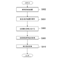
- a method of correcting the critical angle for total reflection will be described with reference to the flowchart shown in FIG.
- a standard sample is placed on the sample table 102 (S902).
- a silicon substrate having a known total reflection critical angle is arranged on the sample stage 102.
- FIG. 4 is a differential curve obtained by measuring the intensity of a Si-k ⁇ ray as the fluorescent X-ray 116 using a silicon substrate that can be used as a standard sample. Although the silicon substrate has a known total reflection critical angle, the known value may be different from the peak angle of the differential curve. The reason for the difference is that the actual incident angle of the primary X-rays 114 on the measurement sample 112 and the incident angle recognized by the total reflection X-ray fluorescence spectrometer 100 depend on the accuracy of machining and assembly, changes over time, etc. This is because there is a case where a difference is made.
- the arithmetic unit acquires the difference between the critical angle for total reflection acquired in S908 and the known critical angle for total reflection of the standard sample as a correction value (S910).
- the correction value is used in step S210, which is a process of calculating the density.
- the total reflection X-ray fluorescence spectrometer 100 may adjust the inclination of the sample table 102 based on the correction value acquired in S910. By adjusting the inclination of the sample stage 102, the incident angle of the actual primary X-ray 114 on the measurement sample 112 and the incident angle recognized by the total reflection X-ray fluorescence analyzer 100 can be matched. it can.
- the density, film thickness, and surface roughness of the measurement sample 112 can be easily measured at low cost by the total reflection X-ray fluorescence spectrometer 100.
- the present invention is not limited to the above embodiment, and various modifications are possible.
- the configuration of the total reflection X-ray fluorescence analyzer 100 is an example, and the present invention is not limited to this. It may be replaced with a configuration substantially the same as the configuration shown in the above embodiment, a configuration having the same operation and effect, or a configuration achieving the same object.
- the total reflection X-ray fluorescence spectrometer 100 adjusts the density measurement mode for measuring the density, the film thickness measurement mode for measuring the film thickness, the surface roughness measurement mode for measuring the surface roughness, and the inclination of the sample table 102.
- Each of the maintenance modes may be configured as a device that can be individually executed according to a user's instruction.
Landscapes
- Physics & Mathematics (AREA)
- Chemical & Material Sciences (AREA)
- General Physics & Mathematics (AREA)
- Biochemistry (AREA)
- Life Sciences & Earth Sciences (AREA)
- Analytical Chemistry (AREA)
- Health & Medical Sciences (AREA)
- General Health & Medical Sciences (AREA)
- Immunology (AREA)
- Pathology (AREA)
- Crystallography & Structural Chemistry (AREA)
- Electromagnetism (AREA)
- Analysing Materials By The Use Of Radiation (AREA)
- Length-Measuring Devices Using Wave Or Particle Radiation (AREA)
Abstract
La présente invention permet de réaliser, à faible coût et de manière simplifiée : un procédé de mesure de la densité et de l'épaisseur d'un échantillon de mesure ; et un dispositif d'analyse de fluorescence X à réflexion totale, pour mesurer la densité et l'épaisseur d'un échantillon de mesure. Ce dispositif d'analyse de fluorescence X à réflexion totale comprend : une source de rayons X, qui émet un rayon X primaire monochromatique tout en changeant l'angle d'incidence par rapport à la surface d'un échantillon de mesure dans une plage couvrant l'angle critique de réflexion totale de l'échantillon de mesure ; un détecteur, pour mesurer l'intensité d'un rayon X fluorescent résultant, généré à partir de l'échantillon de mesure ; et une unité de calcul, qui acquiert une courbe différentielle par différenciation, par rapport à l'angle d'incidence, de la relation entre l'intensité de rayons X fluorescents et l'angle d'incidence, qui acquiert l'angle critique de réflexion totale à partir de la courbe différentielle, et qui, en fonction de l'angle critique de réflexion totale et de la longueur d'onde du rayon X primaire, calcule la densité et/ou l'épaisseur de l'échantillon de mesure.
Applications Claiming Priority (2)
| Application Number | Priority Date | Filing Date | Title |
|---|---|---|---|
| JP2018122155A JP2020003306A (ja) | 2018-06-27 | 2018-06-27 | 全反射蛍光x線分析装置及び測定方法 |
| JP2018-122155 | 2018-06-27 |
Publications (1)
| Publication Number | Publication Date |
|---|---|
| WO2020003675A1 true WO2020003675A1 (fr) | 2020-01-02 |
Family
ID=68986999
Family Applications (1)
| Application Number | Title | Priority Date | Filing Date |
|---|---|---|---|
| PCT/JP2019/014524 Ceased WO2020003675A1 (fr) | 2018-06-27 | 2019-04-01 | Dispositif d'analyse par fluorescence de rayons x à réflexion totale et procédé de mesure |
Country Status (2)
| Country | Link |
|---|---|
| JP (1) | JP2020003306A (fr) |
| WO (1) | WO2020003675A1 (fr) |
Cited By (1)
| Publication number | Priority date | Publication date | Assignee | Title |
|---|---|---|---|---|
| CN116379968A (zh) * | 2022-12-22 | 2023-07-04 | 昆明理工大学 | 一种xrd阵列探测器测量x射线全反射角的方法 |
Citations (7)
| Publication number | Priority date | Publication date | Assignee | Title |
|---|---|---|---|---|
| JPH07260712A (ja) * | 1994-03-18 | 1995-10-13 | Fujitsu Ltd | 試料アライメント方法およびx線装置 |
| JPH08274137A (ja) * | 1995-03-31 | 1996-10-18 | Matsushita Electric Ind Co Ltd | 全反射角度設定方法 |
| WO1997006430A1 (fr) * | 1995-08-09 | 1997-02-20 | Asahi Kasei Kogyo Kabushiki Kaisha | Procede et equipement de spectroscopie par fluorescence aux rayons x a reflexion totale |
| JP2000131248A (ja) * | 1998-10-21 | 2000-05-12 | Rigaku Industrial Co | X線分析方法および装置 |
| US6173036B1 (en) * | 1997-08-01 | 2001-01-09 | Advanced Micro Devices, Inc. | Depth profile metrology using grazing incidence X-ray fluorescence |
| JP2009075018A (ja) * | 2007-09-21 | 2009-04-09 | Technos:Kk | 蛍光x線分析装置および蛍光x線分析方法 |
| JP2009288016A (ja) * | 2008-05-28 | 2009-12-10 | National Institute Of Advanced Industrial & Technology | 蛍光x線分析装置及びそれを用いた半導体装置の評価システム |
-
2018
- 2018-06-27 JP JP2018122155A patent/JP2020003306A/ja active Pending
-
2019
- 2019-04-01 WO PCT/JP2019/014524 patent/WO2020003675A1/fr not_active Ceased
Patent Citations (7)
| Publication number | Priority date | Publication date | Assignee | Title |
|---|---|---|---|---|
| JPH07260712A (ja) * | 1994-03-18 | 1995-10-13 | Fujitsu Ltd | 試料アライメント方法およびx線装置 |
| JPH08274137A (ja) * | 1995-03-31 | 1996-10-18 | Matsushita Electric Ind Co Ltd | 全反射角度設定方法 |
| WO1997006430A1 (fr) * | 1995-08-09 | 1997-02-20 | Asahi Kasei Kogyo Kabushiki Kaisha | Procede et equipement de spectroscopie par fluorescence aux rayons x a reflexion totale |
| US6173036B1 (en) * | 1997-08-01 | 2001-01-09 | Advanced Micro Devices, Inc. | Depth profile metrology using grazing incidence X-ray fluorescence |
| JP2000131248A (ja) * | 1998-10-21 | 2000-05-12 | Rigaku Industrial Co | X線分析方法および装置 |
| JP2009075018A (ja) * | 2007-09-21 | 2009-04-09 | Technos:Kk | 蛍光x線分析装置および蛍光x線分析方法 |
| JP2009288016A (ja) * | 2008-05-28 | 2009-12-10 | National Institute Of Advanced Industrial & Technology | 蛍光x線分析装置及びそれを用いた半導体装置の評価システム |
Cited By (1)
| Publication number | Priority date | Publication date | Assignee | Title |
|---|---|---|---|---|
| CN116379968A (zh) * | 2022-12-22 | 2023-07-04 | 昆明理工大学 | 一种xrd阵列探测器测量x射线全反射角的方法 |
Also Published As
| Publication number | Publication date |
|---|---|
| JP2020003306A (ja) | 2020-01-09 |
Similar Documents
| Publication | Publication Date | Title |
|---|---|---|
| US7068753B2 (en) | Enhancement of X-ray reflectometry by measurement of diffuse reflections | |
| JP3889851B2 (ja) | 膜厚測定方法 | |
| US7103142B1 (en) | Material analysis using multiple X-ray reflectometry models | |
| JP2009536354A (ja) | 比反射率測定法を用いて反射率計を精密に校正する方法と装置 | |
| WO1997006430A1 (fr) | Procede et equipement de spectroscopie par fluorescence aux rayons x a reflexion totale | |
| US20020031164A1 (en) | Method and apparatus for photothermal analysis of a layer of material, especially for thickness measurement thereof | |
| US8011830B2 (en) | Method and system for calibrating an X-ray photoelectron spectroscopy measurement | |
| TWI741526B (zh) | 沉積加工的監控方法及系統 | |
| JP6912045B2 (ja) | 膜厚測定方法およびその装置 | |
| JP2020003306A (ja) | 全反射蛍光x線分析装置及び測定方法 | |
| CN110132188A (zh) | 一种基于多元素x射线特征光谱综合分析的涂渗层厚度计算方法 | |
| JP5874108B2 (ja) | 蛍光x線分析装置 | |
| EP1521947B1 (fr) | Procede de spectres de diffusion pour analyse par fluorescence des rayons x avec des composantes optiques | |
| JP2009074954A (ja) | 蛍光x線分析装置およびそれに用いるプログラム | |
| JP6713110B2 (ja) | バックグラウンド除去方法及び蛍光x線分析装置 | |
| TWI345055B (en) | Method and apparatus for inspection,and cluster tool and apparatus for producing microelectronic devices | |
| JP2006313132A (ja) | 試料分析方法およびx線分析装置 | |
| JPH09269305A (ja) | 蛍光x線分析方法および装置 | |
| JP2025074765A (ja) | X線測定装置 | |
| JP7249666B2 (ja) | 蛍光x線分析装置 | |
| JP7233756B2 (ja) | 蛍光x線分析装置 | |
| JP3488918B2 (ja) | 蛍光x線分析装置 | |
| JP2819716B2 (ja) | X線分光法による薄膜定量及び膜厚測定法 | |
| JPWO2025041264A5 (fr) | ||
| JP2984253B1 (ja) | グロー放電発光分光分析方法および装置 |
Legal Events
| Date | Code | Title | Description |
|---|---|---|---|
| 121 | Ep: the epo has been informed by wipo that ep was designated in this application |
Ref document number: 19826893 Country of ref document: EP Kind code of ref document: A1 |
|
| NENP | Non-entry into the national phase |
Ref country code: DE |
|
| 122 | Ep: pct application non-entry in european phase |
Ref document number: 19826893 Country of ref document: EP Kind code of ref document: A1 |