WO2020003815A1 - Miセンサ、及び、miセンサの製造方法 - Google Patents
Miセンサ、及び、miセンサの製造方法 Download PDFInfo
- Publication number
- WO2020003815A1 WO2020003815A1 PCT/JP2019/020076 JP2019020076W WO2020003815A1 WO 2020003815 A1 WO2020003815 A1 WO 2020003815A1 JP 2019020076 W JP2019020076 W JP 2019020076W WO 2020003815 A1 WO2020003815 A1 WO 2020003815A1
- Authority
- WO
- WIPO (PCT)
- Prior art keywords
- coil
- groove
- layer
- sensor
- outer peripheral
- Prior art date
- Legal status (The legal status is an assumption and is not a legal conclusion. Google has not performed a legal analysis and makes no representation as to the accuracy of the status listed.)
- Ceased
Links
Images


Classifications
-
- G—PHYSICS
- G01—MEASURING; TESTING
- G01R—MEASURING ELECTRIC VARIABLES; MEASURING MAGNETIC VARIABLES
- G01R33/00—Arrangements or instruments for measuring magnetic variables
- G01R33/02—Measuring direction or magnitude of magnetic fields or magnetic flux
- G01R33/06—Measuring direction or magnitude of magnetic fields or magnetic flux using galvano-magnetic devices
- G01R33/063—Magneto-impedance sensors; Nanocristallin sensors
-
- G—PHYSICS
- G01—MEASURING; TESTING
- G01R—MEASURING ELECTRIC VARIABLES; MEASURING MAGNETIC VARIABLES
- G01R3/00—Apparatus or processes specially adapted for the manufacture or maintenance of measuring instruments, e.g. of probe tips
-
- G—PHYSICS
- G01—MEASURING; TESTING
- G01R—MEASURING ELECTRIC VARIABLES; MEASURING MAGNETIC VARIABLES
- G01R33/00—Arrangements or instruments for measuring magnetic variables
- G01R33/0005—Geometrical arrangement of magnetic sensor elements; Apparatus combining different magnetic sensor types
-
- G—PHYSICS
- G01—MEASURING; TESTING
- G01R—MEASURING ELECTRIC VARIABLES; MEASURING MAGNETIC VARIABLES
- G01R33/00—Arrangements or instruments for measuring magnetic variables
- G01R33/0052—Manufacturing aspects; Manufacturing of single devices, i.e. of semiconductor magnetic sensor chips
-
- H—ELECTRICITY
- H01—ELECTRIC ELEMENTS
- H01F—MAGNETS; INDUCTANCES; TRANSFORMERS; SELECTION OF MATERIALS FOR THEIR MAGNETIC PROPERTIES
- H01F27/00—Details of transformers or inductances, in general
- H01F27/28—Coils; Windings; Conductive connections
-
- H—ELECTRICITY
- H01—ELECTRIC ELEMENTS
- H01F—MAGNETS; INDUCTANCES; TRANSFORMERS; SELECTION OF MATERIALS FOR THEIR MAGNETIC PROPERTIES
- H01F41/00—Apparatus or processes specially adapted for manufacturing or assembling magnets, inductances or transformers; Apparatus or processes specially adapted for manufacturing materials characterised by their magnetic properties
- H01F41/02—Apparatus or processes specially adapted for manufacturing or assembling magnets, inductances or transformers; Apparatus or processes specially adapted for manufacturing materials characterised by their magnetic properties for manufacturing cores, coils, or magnets
- H01F41/04—Apparatus or processes specially adapted for manufacturing or assembling magnets, inductances or transformers; Apparatus or processes specially adapted for manufacturing materials characterised by their magnetic properties for manufacturing cores, coils, or magnets for manufacturing coils
- H01F41/041—Printed circuit coils
- H01F41/046—Printed circuit coils structurally combined with ferromagnetic material
-
- H—ELECTRICITY
- H01—ELECTRIC ELEMENTS
- H01F—MAGNETS; INDUCTANCES; TRANSFORMERS; SELECTION OF MATERIALS FOR THEIR MAGNETIC PROPERTIES
- H01F5/00—Coils
- H01F5/003—Printed circuit coils
Definitions
- the present invention relates to an MI sensor and a method for manufacturing the MI sensor, and more particularly, to a technique for manufacturing an MI sensor with a simple configuration.
- an MI (Magneto Impedance: magnetic impedance) sensor including a magnetic conductor made of an amorphous wire and an electromagnetic coil wound around the magnetic conductor via an insulator is known (for example, Patent Document 1). 1).
- the above patent document describes an MI sensor in which a metal material containing copper is vacuum-deposited on the outer peripheral surface of an insulator to form a metal film, and then an electromagnetic coil is formed by selective etching.
- an MI sensor In order to sense a static characteristic or a dynamic characteristic of a target object in three dimensions (or two dimensions), an MI sensor usually includes three (or two) MI elements orthogonal to each other, X and Y, as in the above-described related art. , Z directions.
- Each MI element uses an amorphous magnetic conductor at the center axis, and a coil (pickup coil) is formed so as to wind around the magnetic conductor. Then, a pulse current is applied to the magnetic conductor, and the reaction is detected by the coil.
- the upper and lower parts of the coil must be formed separately, so that the number of turns cannot be increased freely.
- the cross section of the coil cannot be made circular, and the distance between the magnetic conductor and the coil is not constant, resulting in electrical loss.
- MIFurthermore in the case of an MI element in which a coil is formed by winding a wire such as an enamel wire around an air-core cylindrical material, the number of turns of the coil can be set relatively freely.
- a magnetic conductor must be inserted as a core wire after the coil is formed, resulting in a space between the core wire and the coil, resulting in an electrical loss.
- Such an electric loss causes a variation in the detection accuracy of the MI element and also causes an individual difference of the MI element.
- the present invention has been made in view of the circumstances as described above, and the problem to be solved by the present invention is to simplify the mounting work and to keep the distance constant without opening a space between the magnetic conductor and the coil. And an MI sensor and a method of manufacturing the MI sensor, which can reduce the electrical loss and suppress the occurrence of individual differences between the MI sensors and individual differences in the X, Y, and Z directions in the MI sensor. To provide.
- the present invention provides an MI sensor and a method of manufacturing the MI sensor configured as follows in order to solve the above problems.
- An MI sensor includes a linear magnetic conductor, an insulator layer formed on an outer peripheral surface of the magnetic conductor, and a first coil spirally formed on an outer peripheral surface of the insulator layer.
- a second coil, and a MI coil comprising a third coil, wherein the first coil, the second coil, and the third coil are formed of a conductive layer, the first coil, the second coil, And the third coils are arranged in directions orthogonal to each other.
- a method of manufacturing an MI sensor includes the steps of: forming an insulating layer on the outer peripheral surface of a linear magnetic conductor; forming an insulating layer on the outer peripheral surface of the insulating layer; Layer forming step, forming a resist layer on the outer peripheral surface of the conductive layer, the resist step, by exposing the resist layer with a laser, the spiral first groove on the outer peripheral surface of the resist layer, A second gap, and a first gap that forms a third groove, and that goes around the resist layer between the first groove and the second groove on the outer peripheral surface of the resist layer. Forming a second gap around the resist layer between the second groove portion and the third groove portion on the outer peripheral surface of the resist layer, and exposing the resist layer.
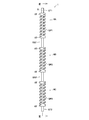
- FIG. 2 is a perspective view showing the MI sensor according to the first embodiment.
- the front view which shows the MI sensor in the middle of manufacture.
- FIG. 3 is a partial sectional view taken along line III-III in FIG. 2.
- FIG. 6 is a view showing each manufacturing process of the MI sensor according to the first embodiment.
- the MI sensor 1A includes a coil 6 (X-axis coil 6X, Y-axis coil 6Y, and Z-axis coil 6Z) that responds to a change in a current flowing through a linear magnetic conductor (the amorphous wire 2 in this embodiment). Magnetic sensing is performed using a so-called MI phenomenon in which an induced voltage is generated.
- the above-mentioned MI phenomenon occurs in a magnetic conductor made of a magnetic material having an electron spin arrangement in a circumferential direction with respect to a supplied current direction.
- the magnetic field in the circumferential direction changes abruptly, and the action of the change in the magnetic field causes a change in the spin direction of electrons according to the peripheral magnetic field.
- the phenomenon in which the internal magnetization and impedance of the magnetic conductor change at that time is the MI phenomenon.
- an MI sensor 1A includes an amorphous wire 2 having a circular outer peripheral shape, such as CoFeSiB having a diameter of several tens of ⁇ m or less, as a linear magnetic conductor. Is used.
- the output voltage per turn of the coil 6 is increased and the number of windings is reduced by using the amorphous wire 2 having excellent magnetic sensing performance as the magnetic conductor, and the axial direction of the MI sensor 1A is reduced. Is configured to be short.
- An insulator layer 3 made of an acrylic resin is formed on the outer periphery of the amorphous wire 2 so that the outer periphery in the cross section is circular.
- a linear body coated with a magnetic anisotropic thin film, a permalloy made of a Ni—Fe alloy, or the like is used in place of the amorphous wire 2 employed in the present embodiment. It is also possible to employ.
- the outer peripheral shape of the insulator layer 3 is formed in a circular shape concentric with the outer peripheral shape of the amorphous wire 2, that is, the insulator layer 3 is formed so that the thickness thereof is uniform in the circumferential direction.
- the amorphous wire 2 is immersed in an electrodeposition paint in which an acrylic resin material is dispersed in a liquid state in an ionic state, and a voltage is applied between the amorphous wire 2 and the electrodeposition paint in the tank. Is applied, the acrylic resin in an ionic state is electrodeposited on the amorphous wire. According to this method, the thickness of the insulating layer can be controlled by the applied voltage.
- the insulator layer 3 is formed by baking the electrodeposition paint formed on the surface of the amorphous wire 2 at a high temperature of, for example, 100 degrees or more.
- the core wire S is constituted by the amorphous wire 2 and the insulator layer 3.
- each of the coils 6X to 6Z is formed of a conductive layer.
- the conductive layers of the coils 6X to 6Z are formed of two layers: an electroless plating layer 4 and an electrolytic plating layer 5 formed on the outer peripheral surface of the electroless plating layer 4 (see FIG. 3). ).
- the configuration of the conductive layers of the coils 6X to 6Z in the present embodiment is an example, and the conductive layers may have other configurations.
- the conductive layers of the coils 6X to 6Z can be formed using a technique such as sputtering.
- the X-axis coil 6X, the Y-axis coil 6Y, and the Z-axis coil 6Z have a core wire S between the X-axis coil 6X and the Y-axis coil 6Y, and the Y-axis coil 6Y and the Z-axis coil 6Z.
- they By being bent between the first and second positions, they are arranged with their axes oriented in the X-axis direction, the Y-axis direction, and the Z-axis direction. That is, the X-axis coil 6X, the Y-axis coil 6Y, and the Z-axis coil 6Z are arranged in directions orthogonal to each other.
- the core S is partially cut off between the X-axis coil 6X and the Y-axis coil 6Y and between the Y-axis coil 6Y and the Z-axis coil 6Z, and the X-axis coil is reconnected.
- the 6X, Y-axis coil 6Y, and Z-axis coil 6Z can be arranged in directions orthogonal to each other.
- both ends of the X-axis coil 6X, the Y-axis coil 6Y, and the Z-axis coil 6Z are formed as annular coil electrodes 6T that go around the insulator layer 3.
- Wirings 7X to 7Z for measuring induced voltages generated in the coils 6X to 6Z are connected to the respective coil electrodes 6T.
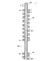
- FIG. 2 is a front view showing the MI sensor (hereinafter, referred to as a “linear sensor”) 1 before the core wire S is bent.
- a linear sensor In the linear sensor 1, a first coil 6A, a second coil 6B, and a third coil 6C are formed.
- a spiral first groove GP1 is formed in the first coil 6A.
- a second groove GP2 is formed in the second coil 6B, and a third groove GP3 is formed in the third coil 6C.
- a first gap portion GQ1 having only the core wire S is formed between the first coil 6A and the second coil 6B, and between the second coil 6B and the third coil 6C, a second gap portion having only the core wire S is formed.
- the portion GQ2 is formed.
- a first terminal GT1 having only the core wire S is formed on the outer end side of the first coil 6A, and a second terminal GT2 having only the core wire S is formed on the outer end side of the third coil 6C.
- the core wire S is orthogonally bent in the first gap GQ1 and the second gap GQ2.
- the MI sensor 1A in which the first coil 6A, the second coil 6B, and the third coil 6C are orthogonal to each other as the X-axis coil 6X, the Y-axis coil 6Y, and the Z-axis coil 6Z is configured.
- FIG. 4 (a) is the amorphous wire 2 before the insulating step, (b) is the state after the insulating step, (c) is the state after the electroless plating step, (d) is the state after the electrolytic plating step, e) shows the state after the resist step, (f) shows the state after the exposure step, (g) shows the state after the etching step, and (h) shows the state after the resist removing step. Note that since the linear sensor 1 is formed by repeating the same configuration in the longitudinal direction, only one end (the periphery of the first coil 6A) is shown in FIG. 4 and the other end is not shown. are doing.
- an amorphous wire 2 having a circular striated outer peripheral shape is prepared.
- an insulator is applied to the outer periphery of the amorphous wire 2 to form an insulator layer 3 (insulation step).
- the outer peripheral shape in the cross section of the insulator layer 3 is made a circular shape concentric with the outer peripheral shape of the amorphous wire 2, that is, the thickness of the insulator layer 3 is uniform in the circumferential direction. It forms so that it may become.
- a conductive layer composed of the electroless plating layer 4 and the electrolytic plating layer 5 is formed on the outer peripheral surface of the insulator layer 3 (conductive layer forming step).
- the electroless plating layer 4 is formed on the outer peripheral surface of the insulator layer 3 by performing electroless Cu plating (electroless plating step). In this step, it is also possible to employ electroless Au plating.
- electrolytic Cu plating is performed to form an electrolytic plating layer 5 on the outer peripheral surface of the electroless plating layer 4 (electrolytic plating step). In this step, it is also possible to employ electrolytic Au plating.
- the metal film is formed on the insulator layer 3 using electroless plating and electrolytic plating.
- the amorphous wire 2 on which the electrolytic plating layer 5 is formed is immersed in a photoresist bath containing a photoresist solution, and is then pulled up at a predetermined speed (for example, at a speed of 1 mm / sec) to obtain a structure shown in FIG.
- a resist layer R is formed on the outer peripheral surface of the electrolytic plating layer 5 (resist step).
- the resist layer R is exposed to a laser, and the portion exposed to the laser is dissolved in a developing solution to form a spiral first groove on the outer peripheral surface of the resist layer R.
- the ridge GA1, the second groove GA2 (and the third groove GA3, not shown) are formed.
- a second gap GB2 (not shown) is formed around the resist layer R with the portion GA3.
- a first end portion GC1 that makes a round around the resist layer R on the outer end side of the first groove portion GA1 on the outer peripheral surface of the resist layer R (and a round of the resist layer R on the outer end side beyond the third groove portion GA3). (Not shown) to form a second end portion GC2).
- the layer 5 is exposed (exposure step).
- the laser exposure in the above exposure step is performed while rotating around the central axis of the amorphous wire 2 on which the resist layer R is formed and displacing in the axial direction.
- the portions exposed to the laser are dissolved in the developing solution, so that various grooves (first groove portions GA1, second groove portions GA2, third groove portions GA3, A positive photoresist in which one gap GB1, a second gap GB2, a first end GC1, and a second end GC2) are formed is employed.
- this step it is also possible to use a negative photoresist in which a portion not exposed to the laser is dissolved in a developing solution to form various grooves in the resist layer.
- the first end portion GC1, the first groove portion GA1, the first gap GB1, and the second groove portion GA2 are formed separately from each other. I have. Similarly, the second groove portion GA2, the second gap GB2, the third groove portion GA3, and the second end portion GC2 are formed apart from each other.
- the amorphous wire 2 in which various grooves are formed in the resist layer R is immersed in an acidic electrolytic polishing solution and subjected to electrolytic polishing, so that the resist layer remaining on the outer periphery of the electrolytic plating layer 5 is used as a masking material. Etching is performed. As a result, as shown in FIG. 4G, the electroless plating layer 4 and the electrolytic plating layer 5 in the portions where various grooves are formed in the resist layer R are removed (etching step).
- a spiral first groove GP1 is formed in the portion of the electroless plating layer 4 and the electrolytic plating layer 5 where the first groove portion GA1 was formed.
- a spiral second groove GP2 is formed in a portion where the second groove GA2 is formed, and a spiral third groove GP3 is formed in a portion where the third groove GA3 is formed.
- the first coil 6A is formed by the electroless plating layer 4 and the electrolytic plating layer 5 remaining around the first groove portion GA1.
- the second coil 6B and the third coil 6C are formed by the electroless plating layer 4 and the electrolytic plating layer 5 remaining around the second groove portion GA2 and the third groove portion GA3.
- a first gap GQ1 and a second gap GQ2 are formed in a portion where the first gap GB1 and the second gap GB2 are formed. Further, a first terminal GT1 and a second terminal GT2 are formed in a portion where the first end GC1 and the second end GC2 are formed.
- the first groove portion GA1 is formed to be separated from the first end portion GC1 and the first gap GB1.
- the electroless plating layer 4 and the electrolytic plating layer 5 remaining at both ends of the first coil 6A are formed as the annular coil electrode 6T that goes around the insulator layer 3.
- the coil electrodes 6T are formed at both ends of the second coil 6B.
- the coil electrodes 6T are formed at both ends of the third coil 6C.
- the resist layer R remaining on the surfaces of the first to third coils 6A to 6C is removed using a stripping solution or the like (resist removing step).
- the linear sensor 1 is bent orthogonally at the first gap GQ1 and the second gap GQ2, thereby forming the MI sensor 1A in which the X-axis coil 6X, the Y-axis coil 6Y, and the Z-axis coil 6Z are orthogonal to each other. (Bending process).
- the MI sensor 1A integrally including the X-axis coil 6X, the Y-axis coil 6Y, and the Z-axis coil 6Z can be manufactured. Thereby, when mounting the MI sensor 1A, there is no need to combine a plurality of MI elements, so that the mounting operation can be simplified.
- a pulse current may be supplied by connecting wiring to each of the first terminal GT1 and the second terminal GT2. That is, since two wires for supplying current to the amorphous wire 2 can be provided, it is possible to mount the amorphous wire 2 more easily as compared with a configuration in which wiring is performed for each of the three MI elements in the related art.
- the manufacturing method of the MI sensor 1A in the insulating step, by forming the outer peripheral shape in the cross section of the insulator layer 3 into a circular shape, the thickness of the insulator layer 3 in the circumferential direction is increased. Formed uniformly. Thereby, the distance can be made constant without opening a space between the amorphous wire 2 and the coil 6 formed on the outer peripheral surface of the insulator layer 3. More specifically, the gap between the amorphous wire 2 and the coil 6 can be concentrically filled with the insulator layer 3 which is a substance having a known magnetic permeability and dielectric constant. For this reason, since the electrical loss in the coil 6 can be reduced, the sensitivity of the MI sensor 1A can be improved.
- the thickness of the insulator layer 3 is reduced by forming the circular insulator layer 3 on the surface of the amorphous wire 2 having a circular cross section. It is formed uniformly in the circumferential direction. For this reason, the distance between the amorphous wire 2 and the coil 6 can be constant regardless of the position in the circumferential direction. As a result, variations in the detection accuracy of the MI sensor 1A can be reduced, and individual differences between the MI sensors 1A can be suppressed. Further, in the method of manufacturing the MI sensor 1A according to the present embodiment, individual differences of the MI sensors 1A can be suppressed because a large number of MI sensors 1A can be manufactured at once by the same process.
- the MI sensor 1A in the MI sensor 1A according to the present embodiment, it is possible to unify the pulses applied to the core wires of the coils 6 arranged in the X, Y, and Z directions without connecting them externally. That is, the same stimulus pulse can be given to the sensor (coil 6) in each direction without strict control. This makes it possible to suppress the occurrence of individual differences in the X, Y, and Z directions in the MI sensor 1A. Since the X-axis coil 6X, the Y-axis coil 6Y, and the Z-axis coil 6Z are orthogonal to each other, no mutual inductance is generated.
- the mounting operation can be simplified, and the electrical distance is maintained by keeping the distance between the amorphous wire 2 and the coil 6 constant without opening a space.
- the MI sensor 1A that can reduce a large loss and suppress occurrence of individual differences and individual differences in the X, Y, and Z directions.
- an annular coil electrode 6T surrounding the insulator layer 3 is formed at both ends of the X-axis coil 6X, the Y-axis coil 6Y, and the Z-axis coil 6Z. I have. This allows the wirings 7X to 7Z to be connected to the coil electrodes 6T irrespective of the postures of the coils 6X to 6Z, thereby making it possible to perform the mounting operation more easily.
- MI sensor 1B (second embodiment)> Next, the configuration of the MI sensor 1B according to the second embodiment of the present invention will be described with reference to FIG. In the present embodiment, a detailed description of a configuration common to the MI sensor 1A according to the first embodiment will be omitted, and a different configuration will be mainly described.
- the MI sensor 1B includes an X-axis coil 6X as a first coil, a Y-axis coil 6Y as a second coil, and a Z-axis as a third coil arranged in a bending step.
- the coil 6 ⁇ / b> Z is manufactured by going through a fixing step (fixing step) with a resin mold P which is a fixing portion.
- the resin mold P is formed in a regular hexahedron, and each surface is formed in a shape orthogonal to the X axis, the Y axis, and the Z axis.
- each of the X-axis coil 6X, the Y-axis coil 6Y, and the Z-axis coil 6Z is accommodated in an internal area (area filled with the resin mold P) of a regular hexahedron formed by the resin mold P. , Are fixedly arranged in a direction orthogonal to the respective surfaces forming the surface of the resin mold P.
- the X-axis coil 6X, the Y-axis coil 6Y, and the Z-axis coil 6Z can be fixed, the X-axis coil 6X, the Y-axis coil 6Y can be determined only by determining the position of the resin mold P. , And the position of the Z-axis coil 6Z can be determined. That is, the mounting operation of the MI sensor 1B can be simplified as compared with the MI sensor 1A according to the embodiment.
- the X-axis coil 6X, the Y-axis coil 6Y, and the Z-axis coil 6Z in the MI sensor 1B are fixed by clips instead of using the resin mold P employed in the present embodiment.
- Other methods such as a method and a method of filling and fixing a sealant around each coil, can be adopted.
- an MI sensor includes a linear magnetic conductor, an insulator layer formed on an outer peripheral surface of the magnetic conductor, and a first spiral formed on the outer peripheral surface of the insulator layer.
- the coil and the third coil are arranged in directions orthogonal to each other.
- the mounting operation can be simplified, the electric loss can be reduced by keeping the distance constant without opening a space between the magnetic conductor and the coil, and the individual difference between the MI sensors and the X in the MI sensor can be reduced. , Y, and Z directions can be suppressed from occurring.
- the first coil, the second coil, and the third coil are fixed by a fixing unit.
- the mounting operation can be further simplified.
- both ends of the first coil, the second coil, and the third coil are formed as annular coil electrodes that go around the insulator layer.
- the mounting operation can be further simplified.
- a method of manufacturing an MI sensor includes the steps of: forming an insulating layer on the outer peripheral surface of a linear magnetic conductor; forming an insulating layer on the outer peripheral surface of the insulating layer; Layer forming step, forming a resist layer on the outer peripheral surface of the conductive layer, the resist step, by exposing the resist layer with a laser, the spiral first groove on the outer peripheral surface of the resist layer, A second gap, and a first gap that forms a third groove, and that goes around the resist layer between the first groove and the second groove on the outer peripheral surface of the resist layer. Forming a second gap around the resist layer between the second groove portion and the third groove portion on the outer peripheral surface of the resist layer, and exposing the resist layer.
- the mounting operation can be simplified, the electrical loss can be reduced by keeping the distance constant without opening a space between the magnetic conductor and the coil, the individual difference between the MI sensors and the MI sensor It is possible to manufacture an MI sensor capable of suppressing the occurrence of individual differences in the X, Y, and Z directions in the above.
- the manufacturing method of the MI sensor includes a fixing step of fixing the first coil, the second coil, and the third coil arranged in the bending step with a fixing portion.
- a first end portion surrounding the resist layer on the outer peripheral surface of the outer peripheral surface of the resist layer with respect to the first groove portion is formed.
- Forming a second end around the resist layer on the outer end side than the third groove on the outer peripheral surface of the layer, the first end, the first groove, the first gap, The second groove, the second gap, the third groove, and the second end are formed separately from each other, and in the etching step, the first coil, the second coil, and the It is preferable that the conductive layer remaining at both ends of each of the three coils is formed as an annular coil electrode that goes around the insulator layer.
- an MI sensor that can further simplify the mounting operation can be manufactured.
- the mounting operation can be simplified, and the electric loss can be reduced by keeping the distance constant without opening a space between the magnetic conductor and the coil. It is possible to suppress the occurrence of individual differences for each MI sensor and individual differences in the X, Y, and Z directions in the MI sensor.
Landscapes
- Physics & Mathematics (AREA)
- Engineering & Computer Science (AREA)
- General Physics & Mathematics (AREA)
- Power Engineering (AREA)
- Condensed Matter Physics & Semiconductors (AREA)
- Chemical & Material Sciences (AREA)
- Nanotechnology (AREA)
- Manufacturing & Machinery (AREA)
- Hall/Mr Elements (AREA)
- Measuring Magnetic Variables (AREA)
Abstract
Description
まず、図1から図3を用いて、本発明の第一実施形態に係る磁気インピーダンスセンサ(以下、単に「MIセンサ」と記載する)1Aの構成について説明する。MIセンサ1Aは、線状の磁性導体(本実施形態においてはアモルファスワイヤ2)に通電する電流の変化に応じてコイル6(X軸コイル6X、Y軸コイル6Y、及び、Z軸コイル6Z)に誘起電圧が生じる、いわゆるMI現象を利用して磁気センシングを行うものである。
次に、図5を用いて、本発明の第二実施形態に係るMIセンサ1Bの構成について説明する。本実施形態においては、前記第一実施形態に係るMIセンサ1Aと共通する構成については詳細な説明を省略し、異なる構成を中心に説明する。
1A 磁気インピーダンスセンサ(MIセンサ)
1B MIセンサ
2 アモルファスワイヤ(磁性導体)
3 絶縁体層 4 無電解めっき層
5 電解めっき層 6 コイル
6A 第一コイル 6B 第二コイル
6C 第三コイル 6T コイル電極
6X X軸コイル 6Y Y軸コイル
6Z Z軸コイル 7X 配線
7Y 配線 7Z 配線
R レジスト層 P 樹脂モールド(固定部)
GA1 第一溝条部 GA2 第二溝条部
GA3 第三溝条部 GB1 第一間隙
GB2 第二間隙 GC1 第一端部
GC2 第二端部 GP1 第一溝部
GP2 第二溝部 GP3 第三溝部
GQ1 第一間隙部 GQ2 第二間隙部
GT1 第一端子 GT2 第二端子
Claims (6)
- 線状の磁性導体と、
前記磁性導体の外周面に形成される絶縁体層と、
前記絶縁体層の外周面に螺旋状に形成される第一コイル、第二コイル、及び、第三コイルと、を備えるMIセンサであって、
前記第一コイル、第二コイル、及び、第三コイルは、導電層で形成され、
前記第一コイル、第二コイル、及び、第三コイルが互いに直交する方向に配置される、MIセンサ。 - 前記第一コイル、第二コイル、及び、第三コイルが固定部で固定される、請求項1に記載のMIセンサ。
- 前記第一コイル、第二コイル、及び、第三コイルの両端部が前記絶縁体層を一周する環状のコイル電極として形成される、請求項1又は請求項2に記載のMIセンサ。
- 線状の磁性導体の外周面に絶縁体層を形成する、絶縁工程と、
前記絶縁体層の外周面に導電層を形成する、導電層形成工程と、
前記導電層の外周面にレジスト層を形成する、レジスト工程と、
前記レジスト層をレーザーで露光することにより、前記レジスト層の外周面にそれぞれ螺旋状の第一溝条部、第二溝条部、及び、第三溝条部を形成し、前記レジスト層の外周面における前記第一溝条部と前記第二溝条部との間で前記レジスト層を一周する第一間隙を形成し、前記レジスト層の外周面における前記第二溝条部と前記第三溝条部との間で前記レジスト層を一周する第二間隙を形成する、露光工程と、
前記レジスト層をマスキング材としてエッチングを行い、前記第一溝条部、第二溝条部、第三溝条部、第一間隙、及び、第二間隙における前記導電層を除去することにより、前記第一溝条部の周囲に残存する前記導電層で第一コイルを形成し、前記第二溝条部の周囲に残存する前記導電層で第二コイルを形成し、前記第三溝条部の周囲に残存する前記導電層で第三コイルを形成する、エッチング工程と、
前記磁性導体及び前記絶縁体層を、前記第一コイルと前記第二コイルとの間、及び、前記第二コイルと前記第三コイルとの間で折り曲げることにより、前記第一コイル、第二コイル、及び、第三コイルを互いに直交する方向に配置する、折り曲げ工程と、を備える、MIセンサの製造方法。 - 前記折り曲げ工程で配置した前記第一コイル、第二コイル、及び、第三コイルを固定部で固定する、固定工程を備える、請求項4に記載のMIセンサの製造方法。
- 前記露光工程において、前記レジスト層の外周面における前記第一溝条部よりも外端側に前記レジスト層を一周する第一端部を形成し、前記レジスト層の外周面における前記第三溝条部よりも外端側に前記レジスト層を一周する第二端部を形成し、前記第一端部、前記第一溝条部、前記第一間隙、前記第二溝条部、前記第二間隙、前記第三溝条部、及び、前記第二端部を互いに離間して形成し、
前記エッチング工程において、前記第一コイル、第二コイル、及び、第三コイルのそれぞれの両端部で残存する前記導電層が前記絶縁体層を一周する環状のコイル電極として形成される、請求項4又は請求項5に記載のMIセンサの製造方法。
Priority Applications (4)
| Application Number | Priority Date | Filing Date | Title |
|---|---|---|---|
| US17/043,768 US11953562B2 (en) | 2018-06-27 | 2019-05-21 | MI sensor and method for manufacturing MI sensor |
| CN201980043095.6A CN112400116A (zh) | 2018-06-27 | 2019-05-21 | 磁阻抗传感器及磁阻抗传感器的制造方法 |
| KR1020207036896A KR102747798B1 (ko) | 2018-06-27 | 2019-05-21 | Mi 센서 및 mi 센서의 제조 방법 |
| JP2020527282A JP7468344B2 (ja) | 2018-06-27 | 2019-05-21 | Miセンサ、及び、miセンサの製造方法 |
Applications Claiming Priority (2)
| Application Number | Priority Date | Filing Date | Title |
|---|---|---|---|
| JP2018121668 | 2018-06-27 | ||
| JP2018-121668 | 2018-06-27 |
Publications (1)
| Publication Number | Publication Date |
|---|---|
| WO2020003815A1 true WO2020003815A1 (ja) | 2020-01-02 |
Family
ID=68986386
Family Applications (1)
| Application Number | Title | Priority Date | Filing Date |
|---|---|---|---|
| PCT/JP2019/020076 Ceased WO2020003815A1 (ja) | 2018-06-27 | 2019-05-21 | Miセンサ、及び、miセンサの製造方法 |
Country Status (5)
| Country | Link |
|---|---|
| US (1) | US11953562B2 (ja) |
| JP (1) | JP7468344B2 (ja) |
| KR (1) | KR102747798B1 (ja) |
| CN (1) | CN112400116A (ja) |
| WO (1) | WO2020003815A1 (ja) |
Cited By (1)
| Publication number | Priority date | Publication date | Assignee | Title |
|---|---|---|---|---|
| CN111785472A (zh) * | 2020-06-22 | 2020-10-16 | 上海卫星工程研究所 | 双超卫星磁浮低电阻pcb线圈 |
Families Citing this family (2)
| Publication number | Priority date | Publication date | Assignee | Title |
|---|---|---|---|---|
| US11527341B2 (en) * | 2017-02-28 | 2022-12-13 | Nidec-Read Corporation | Coiled electronic component, coil component, manufacturing method of coil component, inductance element, T-type filter, oscillation circuit, and manufacturing method of inductance |
| CN118112470B (zh) * | 2024-05-06 | 2024-06-28 | 中国人民解放军国防科技大学 | 非晶丝探头、制备方法及磁传感器 |
Citations (8)
| Publication number | Priority date | Publication date | Assignee | Title |
|---|---|---|---|---|
| JPH1174582A (ja) * | 1997-08-28 | 1999-03-16 | Alps Electric Co Ltd | 方位センサ |
| JP2001004726A (ja) * | 1999-06-22 | 2001-01-12 | Tdk Corp | 磁界センサ |
| JP2002286823A (ja) * | 2001-03-27 | 2002-10-03 | Stanley Electric Co Ltd | 磁気検出素子及びそれを用いた磁気センサ |
| JP2006047267A (ja) * | 2003-07-18 | 2006-02-16 | Aichi Steel Works Ltd | 3次元磁気方位センサおよびマグネト・インピーダンス・センサ素子 |
| JP2006300906A (ja) * | 2005-04-25 | 2006-11-02 | Aichi Steel Works Ltd | マグネト・インピーダンス・センサ素子 |
| JP2009229101A (ja) * | 2008-03-19 | 2009-10-08 | Kumamoto Univ | 微小コイルおよび微小装置 |
| CN104820196A (zh) * | 2015-04-11 | 2015-08-05 | 西北工业大学 | 一种n形结构低功耗磁通门传感器 |
| JP2016194531A (ja) * | 2016-08-11 | 2016-11-17 | 愛知製鋼株式会社 | 磁界測定装置 |
Family Cites Families (17)
| Publication number | Priority date | Publication date | Assignee | Title |
|---|---|---|---|---|
| JP4047955B2 (ja) * | 1997-10-01 | 2008-02-13 | ミネベア株式会社 | 磁気インピーダンスセンサ |
| JPH11162742A (ja) * | 1997-11-21 | 1999-06-18 | Toko Inc | インダクタンス素子とその製造方法 |
| JP3656018B2 (ja) * | 2000-06-16 | 2005-06-02 | アルプス電気株式会社 | 磁気インピーダンス効果素子の製造方法 |
| JP2004146614A (ja) * | 2002-10-24 | 2004-05-20 | Sony Corp | 磁気抵抗効果素子および磁気メモリ装置 |
| JP3781056B2 (ja) * | 2003-07-18 | 2006-05-31 | 愛知製鋼株式会社 | 3次元磁気方位センサおよびマグネト・インピーダンス・センサ素子 |
| JP5075489B2 (ja) * | 2007-06-06 | 2012-11-21 | 株式会社フジクラ | 磁気デバイスおよびその製造方法 |
| WO2009044820A1 (ja) * | 2007-10-02 | 2009-04-09 | Aichi Steel Corporation | マグネトインピーダンス素子およびマグネトインピーダンスセンサ |
| JP2009236803A (ja) * | 2008-03-28 | 2009-10-15 | Aichi Steel Works Ltd | マグネトインピーダンスセンサ素子 |
| JP4725600B2 (ja) * | 2008-06-10 | 2011-07-13 | 愛知製鋼株式会社 | マグネトインピーダンスセンサ素子 |
| WO2010097932A1 (ja) * | 2009-02-27 | 2010-09-02 | 愛知製鋼株式会社 | マグネトインピーダンスセンサ素子及びその製造方法 |
| JP5110142B2 (ja) * | 2010-10-01 | 2012-12-26 | 愛知製鋼株式会社 | マグネトインピーダンスセンサ素子及びその製造方法 |
| JP2013124989A (ja) * | 2011-12-15 | 2013-06-24 | Oita-Ken Sangyosozokiko | 簡易ベクトル磁気特性測定装置 |
| JP2013205308A (ja) * | 2012-03-29 | 2013-10-07 | Hioki Ee Corp | 磁界センサ |
| EP2908150B1 (en) * | 2012-10-04 | 2017-12-27 | Aichi Steel Corporation | Magneto-impedance element and method for producing the same |
| WO2015025606A1 (ja) * | 2013-08-20 | 2015-02-26 | マグネデザイン株式会社 | 電磁コイル付マグネト・インピーダンス・センサ素子および電磁コイル付マグネト・インピーダンス・センサ |
| KR101693749B1 (ko) * | 2015-04-06 | 2017-01-06 | 삼성전기주식회사 | 인덕터 소자 및 그 제조방법 |
| CN105699921B (zh) * | 2016-01-21 | 2018-05-01 | 中国船舶重工集团公司第七二五研究所 | 一种采用3d打印机制备双轴巨磁阻抗效应磁敏器的方法 |
-
2019
- 2019-05-21 KR KR1020207036896A patent/KR102747798B1/ko active Active
- 2019-05-21 US US17/043,768 patent/US11953562B2/en active Active
- 2019-05-21 JP JP2020527282A patent/JP7468344B2/ja active Active
- 2019-05-21 WO PCT/JP2019/020076 patent/WO2020003815A1/ja not_active Ceased
- 2019-05-21 CN CN201980043095.6A patent/CN112400116A/zh not_active Withdrawn
Patent Citations (8)
| Publication number | Priority date | Publication date | Assignee | Title |
|---|---|---|---|---|
| JPH1174582A (ja) * | 1997-08-28 | 1999-03-16 | Alps Electric Co Ltd | 方位センサ |
| JP2001004726A (ja) * | 1999-06-22 | 2001-01-12 | Tdk Corp | 磁界センサ |
| JP2002286823A (ja) * | 2001-03-27 | 2002-10-03 | Stanley Electric Co Ltd | 磁気検出素子及びそれを用いた磁気センサ |
| JP2006047267A (ja) * | 2003-07-18 | 2006-02-16 | Aichi Steel Works Ltd | 3次元磁気方位センサおよびマグネト・インピーダンス・センサ素子 |
| JP2006300906A (ja) * | 2005-04-25 | 2006-11-02 | Aichi Steel Works Ltd | マグネト・インピーダンス・センサ素子 |
| JP2009229101A (ja) * | 2008-03-19 | 2009-10-08 | Kumamoto Univ | 微小コイルおよび微小装置 |
| CN104820196A (zh) * | 2015-04-11 | 2015-08-05 | 西北工业大学 | 一种n形结构低功耗磁通门传感器 |
| JP2016194531A (ja) * | 2016-08-11 | 2016-11-17 | 愛知製鋼株式会社 | 磁界測定装置 |
Cited By (1)
| Publication number | Priority date | Publication date | Assignee | Title |
|---|---|---|---|---|
| CN111785472A (zh) * | 2020-06-22 | 2020-10-16 | 上海卫星工程研究所 | 双超卫星磁浮低电阻pcb线圈 |
Also Published As
| Publication number | Publication date |
|---|---|
| CN112400116A (zh) | 2021-02-23 |
| KR20210023873A (ko) | 2021-03-04 |
| JP7468344B2 (ja) | 2024-04-16 |
| US20210109169A1 (en) | 2021-04-15 |
| JPWO2020003815A1 (ja) | 2021-08-02 |
| US11953562B2 (en) | 2024-04-09 |
| KR102747798B1 (ko) | 2024-12-31 |
Similar Documents
| Publication | Publication Date | Title |
|---|---|---|
| JP6438963B2 (ja) | スクリーンされたコイルを備える広帯域ロゴスキートランスデューサ | |
| JP4674533B2 (ja) | 交流電流検出用コイル | |
| KR102747798B1 (ko) | Mi 센서 및 mi 센서의 제조 방법 | |
| KR20110120316A (ko) | 마그네토 임피던스 센서 소자 및 그 제조 방법 | |
| JP2017045918A (ja) | コイル部品 | |
| JP2009236803A (ja) | マグネトインピーダンスセンサ素子 | |
| US10823763B2 (en) | Device for measuring electric currents | |
| US12293864B2 (en) | Coil component and manufacturing method therefor | |
| CN206161700U (zh) | 开口式罗氏线圈 | |
| JP2014220466A (ja) | コイル | |
| JP7480506B2 (ja) | Mi素子の製造方法、及び、mi素子 | |
| JP2009246257A (ja) | コイル部品 | |
| CN110764032B (zh) | 用于光泵磁力仪的射频薄膜 | |
| JP2005085968A (ja) | 巻線型インダクタ及びその製造方法 | |
| JP4632363B2 (ja) | 磁界発生コイル | |
| US11536787B2 (en) | Magnetic field gradient coils with closely packed windings and methods of manufacturing same | |
| JP2025012914A (ja) | 磁気センサ素子 | |
| JP3214661B2 (ja) | 電磁流量計 | |
| JPH10179544A (ja) | Mr装置の傾斜磁場発生用コイル | |
| JP5082282B2 (ja) | インダクタンス部品とその製造方法 | |
| JP2025135701A (ja) | ボイスコイル、及びボイスコイルの製造方法 | |
| JP2025021552A (ja) | コイル部品 | |
| US11538623B2 (en) | Coil component, electronic component, and electronic apparatus | |
| JPS5848877A (ja) | サ−チコイルおよびその製造方法 | |
| CN101478187B (zh) | 马达线圈 |
Legal Events
| Date | Code | Title | Description |
|---|---|---|---|
| 121 | Ep: the epo has been informed by wipo that ep was designated in this application |
Ref document number: 19825571 Country of ref document: EP Kind code of ref document: A1 |
|
| ENP | Entry into the national phase |
Ref document number: 2020527282 Country of ref document: JP Kind code of ref document: A |
|
| ENP | Entry into the national phase |
Ref document number: 20207036896 Country of ref document: KR Kind code of ref document: A |
|
| NENP | Non-entry into the national phase |
Ref country code: DE |
|
| 122 | Ep: pct application non-entry in european phase |
Ref document number: 19825571 Country of ref document: EP Kind code of ref document: A1 |