WO2020004048A1 - Procédé de traitement de substrat - Google Patents
Procédé de traitement de substrat Download PDFInfo
- Publication number
- WO2020004048A1 WO2020004048A1 PCT/JP2019/023407 JP2019023407W WO2020004048A1 WO 2020004048 A1 WO2020004048 A1 WO 2020004048A1 JP 2019023407 W JP2019023407 W JP 2019023407W WO 2020004048 A1 WO2020004048 A1 WO 2020004048A1
- Authority
- WO
- WIPO (PCT)
- Prior art keywords
- voltage
- substrate processing
- susceptor
- chamber
- upper electrodes
- Prior art date
- Legal status (The legal status is an assumption and is not a legal conclusion. Google has not performed a legal analysis and makes no representation as to the accuracy of the status listed.)
- Ceased
Links
Images







Classifications
-
- C—CHEMISTRY; METALLURGY
- C23—COATING METALLIC MATERIAL; COATING MATERIAL WITH METALLIC MATERIAL; CHEMICAL SURFACE TREATMENT; DIFFUSION TREATMENT OF METALLIC MATERIAL; COATING BY VACUUM EVAPORATION, BY SPUTTERING, BY ION IMPLANTATION OR BY CHEMICAL VAPOUR DEPOSITION, IN GENERAL; INHIBITING CORROSION OF METALLIC MATERIAL OR INCRUSTATION IN GENERAL
- C23C—COATING METALLIC MATERIAL; COATING MATERIAL WITH METALLIC MATERIAL; SURFACE TREATMENT OF METALLIC MATERIAL BY DIFFUSION INTO THE SURFACE, BY CHEMICAL CONVERSION OR SUBSTITUTION; COATING BY VACUUM EVAPORATION, BY SPUTTERING, BY ION IMPLANTATION OR BY CHEMICAL VAPOUR DEPOSITION, IN GENERAL
- C23C16/00—Chemical coating by decomposition of gaseous compounds, without leaving reaction products of surface material in the coating, i.e. chemical vapour deposition [CVD] processes
- C23C16/22—Chemical coating by decomposition of gaseous compounds, without leaving reaction products of surface material in the coating, i.e. chemical vapour deposition [CVD] processes characterised by the deposition of inorganic material, other than metallic material
- C23C16/30—Deposition of compounds, mixtures or solid solutions, e.g. borides, carbides, nitrides
- C23C16/34—Nitrides
- C23C16/345—Silicon nitride
-
- H—ELECTRICITY
- H01—ELECTRIC ELEMENTS
- H01J—ELECTRIC DISCHARGE TUBES OR DISCHARGE LAMPS
- H01J37/00—Discharge tubes with provision for introducing objects or material to be exposed to the discharge, e.g. for the purpose of examination or processing thereof
- H01J37/32—Gas-filled discharge tubes
- H01J37/32431—Constructional details of the reactor
- H01J37/32532—Electrodes
- H01J37/32568—Relative arrangement or disposition of electrodes; moving means
-
- C—CHEMISTRY; METALLURGY
- C23—COATING METALLIC MATERIAL; COATING MATERIAL WITH METALLIC MATERIAL; CHEMICAL SURFACE TREATMENT; DIFFUSION TREATMENT OF METALLIC MATERIAL; COATING BY VACUUM EVAPORATION, BY SPUTTERING, BY ION IMPLANTATION OR BY CHEMICAL VAPOUR DEPOSITION, IN GENERAL; INHIBITING CORROSION OF METALLIC MATERIAL OR INCRUSTATION IN GENERAL
- C23C—COATING METALLIC MATERIAL; COATING MATERIAL WITH METALLIC MATERIAL; SURFACE TREATMENT OF METALLIC MATERIAL BY DIFFUSION INTO THE SURFACE, BY CHEMICAL CONVERSION OR SUBSTITUTION; COATING BY VACUUM EVAPORATION, BY SPUTTERING, BY ION IMPLANTATION OR BY CHEMICAL VAPOUR DEPOSITION, IN GENERAL
- C23C14/00—Coating by vacuum evaporation, by sputtering or by ion implantation of the coating forming material
- C23C14/06—Coating by vacuum evaporation, by sputtering or by ion implantation of the coating forming material characterised by the coating material
- C23C14/0641—Nitrides
- C23C14/0652—Silicon nitride
-
- C—CHEMISTRY; METALLURGY
- C23—COATING METALLIC MATERIAL; COATING MATERIAL WITH METALLIC MATERIAL; CHEMICAL SURFACE TREATMENT; DIFFUSION TREATMENT OF METALLIC MATERIAL; COATING BY VACUUM EVAPORATION, BY SPUTTERING, BY ION IMPLANTATION OR BY CHEMICAL VAPOUR DEPOSITION, IN GENERAL; INHIBITING CORROSION OF METALLIC MATERIAL OR INCRUSTATION IN GENERAL
- C23C—COATING METALLIC MATERIAL; COATING MATERIAL WITH METALLIC MATERIAL; SURFACE TREATMENT OF METALLIC MATERIAL BY DIFFUSION INTO THE SURFACE, BY CHEMICAL CONVERSION OR SUBSTITUTION; COATING BY VACUUM EVAPORATION, BY SPUTTERING, BY ION IMPLANTATION OR BY CHEMICAL VAPOUR DEPOSITION, IN GENERAL
- C23C14/00—Coating by vacuum evaporation, by sputtering or by ion implantation of the coating forming material
- C23C14/06—Coating by vacuum evaporation, by sputtering or by ion implantation of the coating forming material characterised by the coating material
- C23C14/10—Glass or silica
-
- C—CHEMISTRY; METALLURGY
- C23—COATING METALLIC MATERIAL; COATING MATERIAL WITH METALLIC MATERIAL; CHEMICAL SURFACE TREATMENT; DIFFUSION TREATMENT OF METALLIC MATERIAL; COATING BY VACUUM EVAPORATION, BY SPUTTERING, BY ION IMPLANTATION OR BY CHEMICAL VAPOUR DEPOSITION, IN GENERAL; INHIBITING CORROSION OF METALLIC MATERIAL OR INCRUSTATION IN GENERAL
- C23C—COATING METALLIC MATERIAL; COATING MATERIAL WITH METALLIC MATERIAL; SURFACE TREATMENT OF METALLIC MATERIAL BY DIFFUSION INTO THE SURFACE, BY CHEMICAL CONVERSION OR SUBSTITUTION; COATING BY VACUUM EVAPORATION, BY SPUTTERING, BY ION IMPLANTATION OR BY CHEMICAL VAPOUR DEPOSITION, IN GENERAL
- C23C14/00—Coating by vacuum evaporation, by sputtering or by ion implantation of the coating forming material
- C23C14/22—Coating by vacuum evaporation, by sputtering or by ion implantation of the coating forming material characterised by the process of coating
- C23C14/221—Ion beam deposition
-
- C—CHEMISTRY; METALLURGY
- C23—COATING METALLIC MATERIAL; COATING MATERIAL WITH METALLIC MATERIAL; CHEMICAL SURFACE TREATMENT; DIFFUSION TREATMENT OF METALLIC MATERIAL; COATING BY VACUUM EVAPORATION, BY SPUTTERING, BY ION IMPLANTATION OR BY CHEMICAL VAPOUR DEPOSITION, IN GENERAL; INHIBITING CORROSION OF METALLIC MATERIAL OR INCRUSTATION IN GENERAL
- C23C—COATING METALLIC MATERIAL; COATING MATERIAL WITH METALLIC MATERIAL; SURFACE TREATMENT OF METALLIC MATERIAL BY DIFFUSION INTO THE SURFACE, BY CHEMICAL CONVERSION OR SUBSTITUTION; COATING BY VACUUM EVAPORATION, BY SPUTTERING, BY ION IMPLANTATION OR BY CHEMICAL VAPOUR DEPOSITION, IN GENERAL
- C23C16/00—Chemical coating by decomposition of gaseous compounds, without leaving reaction products of surface material in the coating, i.e. chemical vapour deposition [CVD] processes
- C23C16/06—Chemical coating by decomposition of gaseous compounds, without leaving reaction products of surface material in the coating, i.e. chemical vapour deposition [CVD] processes characterised by the deposition of metallic material
-
- C—CHEMISTRY; METALLURGY
- C23—COATING METALLIC MATERIAL; COATING MATERIAL WITH METALLIC MATERIAL; CHEMICAL SURFACE TREATMENT; DIFFUSION TREATMENT OF METALLIC MATERIAL; COATING BY VACUUM EVAPORATION, BY SPUTTERING, BY ION IMPLANTATION OR BY CHEMICAL VAPOUR DEPOSITION, IN GENERAL; INHIBITING CORROSION OF METALLIC MATERIAL OR INCRUSTATION IN GENERAL
- C23C—COATING METALLIC MATERIAL; COATING MATERIAL WITH METALLIC MATERIAL; SURFACE TREATMENT OF METALLIC MATERIAL BY DIFFUSION INTO THE SURFACE, BY CHEMICAL CONVERSION OR SUBSTITUTION; COATING BY VACUUM EVAPORATION, BY SPUTTERING, BY ION IMPLANTATION OR BY CHEMICAL VAPOUR DEPOSITION, IN GENERAL
- C23C16/00—Chemical coating by decomposition of gaseous compounds, without leaving reaction products of surface material in the coating, i.e. chemical vapour deposition [CVD] processes
- C23C16/22—Chemical coating by decomposition of gaseous compounds, without leaving reaction products of surface material in the coating, i.e. chemical vapour deposition [CVD] processes characterised by the deposition of inorganic material, other than metallic material
- C23C16/30—Deposition of compounds, mixtures or solid solutions, e.g. borides, carbides, nitrides
- C23C16/40—Oxides
- C23C16/401—Oxides containing silicon
- C23C16/402—Silicon dioxide
-
- C—CHEMISTRY; METALLURGY
- C23—COATING METALLIC MATERIAL; COATING MATERIAL WITH METALLIC MATERIAL; CHEMICAL SURFACE TREATMENT; DIFFUSION TREATMENT OF METALLIC MATERIAL; COATING BY VACUUM EVAPORATION, BY SPUTTERING, BY ION IMPLANTATION OR BY CHEMICAL VAPOUR DEPOSITION, IN GENERAL; INHIBITING CORROSION OF METALLIC MATERIAL OR INCRUSTATION IN GENERAL
- C23C—COATING METALLIC MATERIAL; COATING MATERIAL WITH METALLIC MATERIAL; SURFACE TREATMENT OF METALLIC MATERIAL BY DIFFUSION INTO THE SURFACE, BY CHEMICAL CONVERSION OR SUBSTITUTION; COATING BY VACUUM EVAPORATION, BY SPUTTERING, BY ION IMPLANTATION OR BY CHEMICAL VAPOUR DEPOSITION, IN GENERAL
- C23C16/00—Chemical coating by decomposition of gaseous compounds, without leaving reaction products of surface material in the coating, i.e. chemical vapour deposition [CVD] processes
- C23C16/44—Chemical coating by decomposition of gaseous compounds, without leaving reaction products of surface material in the coating, i.e. chemical vapour deposition [CVD] processes characterised by the method of coating
- C23C16/50—Chemical coating by decomposition of gaseous compounds, without leaving reaction products of surface material in the coating, i.e. chemical vapour deposition [CVD] processes characterised by the method of coating using electric discharges
- C23C16/517—Chemical coating by decomposition of gaseous compounds, without leaving reaction products of surface material in the coating, i.e. chemical vapour deposition [CVD] processes characterised by the method of coating using electric discharges using a combination of discharges covered by two or more of groups C23C16/503 - C23C16/515
-
- H—ELECTRICITY
- H01—ELECTRIC ELEMENTS
- H01J—ELECTRIC DISCHARGE TUBES OR DISCHARGE LAMPS
- H01J37/00—Discharge tubes with provision for introducing objects or material to be exposed to the discharge, e.g. for the purpose of examination or processing thereof
- H01J37/32—Gas-filled discharge tubes
- H01J37/32009—Arrangements for generation of plasma specially adapted for examination or treatment of objects, e.g. plasma sources
- H01J37/32018—Glow discharge
- H01J37/32027—DC powered
-
- H—ELECTRICITY
- H01—ELECTRIC ELEMENTS
- H01J—ELECTRIC DISCHARGE TUBES OR DISCHARGE LAMPS
- H01J37/00—Discharge tubes with provision for introducing objects or material to be exposed to the discharge, e.g. for the purpose of examination or processing thereof
- H01J37/32—Gas-filled discharge tubes
- H01J37/32009—Arrangements for generation of plasma specially adapted for examination or treatment of objects, e.g. plasma sources
- H01J37/32018—Glow discharge
- H01J37/32045—Circuits specially adapted for controlling the glow discharge
-
- H—ELECTRICITY
- H01—ELECTRIC ELEMENTS
- H01J—ELECTRIC DISCHARGE TUBES OR DISCHARGE LAMPS
- H01J37/00—Discharge tubes with provision for introducing objects or material to be exposed to the discharge, e.g. for the purpose of examination or processing thereof
- H01J37/32—Gas-filled discharge tubes
- H01J37/32009—Arrangements for generation of plasma specially adapted for examination or treatment of objects, e.g. plasma sources
- H01J37/32082—Radio frequency generated discharge
- H01J37/32137—Radio frequency generated discharge controlling of the discharge by modulation of energy
- H01J37/32146—Amplitude modulation, includes pulsing
-
- H—ELECTRICITY
- H01—ELECTRIC ELEMENTS
- H01J—ELECTRIC DISCHARGE TUBES OR DISCHARGE LAMPS
- H01J37/00—Discharge tubes with provision for introducing objects or material to be exposed to the discharge, e.g. for the purpose of examination or processing thereof
- H01J37/32—Gas-filled discharge tubes
- H01J37/32009—Arrangements for generation of plasma specially adapted for examination or treatment of objects, e.g. plasma sources
- H01J37/32082—Radio frequency generated discharge
- H01J37/32174—Circuits specially adapted for controlling the RF discharge
-
- H—ELECTRICITY
- H01—ELECTRIC ELEMENTS
- H01J—ELECTRIC DISCHARGE TUBES OR DISCHARGE LAMPS
- H01J37/00—Discharge tubes with provision for introducing objects or material to be exposed to the discharge, e.g. for the purpose of examination or processing thereof
- H01J37/32—Gas-filled discharge tubes
- H01J37/32431—Constructional details of the reactor
- H01J37/32532—Electrodes
- H01J37/32577—Electrical connecting means
-
- H—ELECTRICITY
- H10—SEMICONDUCTOR DEVICES; ELECTRIC SOLID-STATE DEVICES NOT OTHERWISE PROVIDED FOR
- H10P—GENERIC PROCESSES OR APPARATUS FOR THE MANUFACTURE OR TREATMENT OF DEVICES COVERED BY CLASS H10
- H10P14/00—Formation of materials, e.g. in the shape of layers or pillars
- H10P14/40—Formation of materials, e.g. in the shape of layers or pillars of conductive or resistive materials
- H10P14/412—Deposition of metallic or metal-silicide materials
-
- H—ELECTRICITY
- H10—SEMICONDUCTOR DEVICES; ELECTRIC SOLID-STATE DEVICES NOT OTHERWISE PROVIDED FOR
- H10P—GENERIC PROCESSES OR APPARATUS FOR THE MANUFACTURE OR TREATMENT OF DEVICES COVERED BY CLASS H10
- H10P14/00—Formation of materials, e.g. in the shape of layers or pillars
- H10P14/40—Formation of materials, e.g. in the shape of layers or pillars of conductive or resistive materials
- H10P14/418—Formation of materials, e.g. in the shape of layers or pillars of conductive or resistive materials the conductive layers comprising transition metals
-
- H—ELECTRICITY
- H10—SEMICONDUCTOR DEVICES; ELECTRIC SOLID-STATE DEVICES NOT OTHERWISE PROVIDED FOR
- H10P—GENERIC PROCESSES OR APPARATUS FOR THE MANUFACTURE OR TREATMENT OF DEVICES COVERED BY CLASS H10
- H10P14/00—Formation of materials, e.g. in the shape of layers or pillars
- H10P14/40—Formation of materials, e.g. in the shape of layers or pillars of conductive or resistive materials
- H10P14/42—Formation of materials, e.g. in the shape of layers or pillars of conductive or resistive materials using a gas or vapour
-
- H—ELECTRICITY
- H10—SEMICONDUCTOR DEVICES; ELECTRIC SOLID-STATE DEVICES NOT OTHERWISE PROVIDED FOR
- H10P—GENERIC PROCESSES OR APPARATUS FOR THE MANUFACTURE OR TREATMENT OF DEVICES COVERED BY CLASS H10
- H10P14/00—Formation of materials, e.g. in the shape of layers or pillars
- H10P14/40—Formation of materials, e.g. in the shape of layers or pillars of conductive or resistive materials
- H10P14/42—Formation of materials, e.g. in the shape of layers or pillars of conductive or resistive materials using a gas or vapour
- H10P14/43—Chemical deposition, e.g. chemical vapour deposition [CVD]
-
- H—ELECTRICITY
- H10—SEMICONDUCTOR DEVICES; ELECTRIC SOLID-STATE DEVICES NOT OTHERWISE PROVIDED FOR
- H10P—GENERIC PROCESSES OR APPARATUS FOR THE MANUFACTURE OR TREATMENT OF DEVICES COVERED BY CLASS H10
- H10P14/00—Formation of materials, e.g. in the shape of layers or pillars
- H10P14/60—Formation of materials, e.g. in the shape of layers or pillars of insulating materials
-
- H—ELECTRICITY
- H10—SEMICONDUCTOR DEVICES; ELECTRIC SOLID-STATE DEVICES NOT OTHERWISE PROVIDED FOR
- H10P—GENERIC PROCESSES OR APPARATUS FOR THE MANUFACTURE OR TREATMENT OF DEVICES COVERED BY CLASS H10
- H10P14/00—Formation of materials, e.g. in the shape of layers or pillars
- H10P14/60—Formation of materials, e.g. in the shape of layers or pillars of insulating materials
- H10P14/63—Formation of materials, e.g. in the shape of layers or pillars of insulating materials characterised by the formation processes
- H10P14/6326—Deposition processes
- H10P14/6328—Deposition from the gas or vapour phase
- H10P14/6334—Deposition from the gas or vapour phase using decomposition or reaction of gaseous or vapour phase compounds, i.e. chemical vapour deposition
- H10P14/6336—Deposition from the gas or vapour phase using decomposition or reaction of gaseous or vapour phase compounds, i.e. chemical vapour deposition in the presence of a plasma [PECVD]
-
- H—ELECTRICITY
- H10—SEMICONDUCTOR DEVICES; ELECTRIC SOLID-STATE DEVICES NOT OTHERWISE PROVIDED FOR
- H10P—GENERIC PROCESSES OR APPARATUS FOR THE MANUFACTURE OR TREATMENT OF DEVICES COVERED BY CLASS H10
- H10P14/00—Formation of materials, e.g. in the shape of layers or pillars
- H10P14/60—Formation of materials, e.g. in the shape of layers or pillars of insulating materials
- H10P14/66—Formation of materials, e.g. in the shape of layers or pillars of insulating materials characterised by the type of materials
- H10P14/662—Laminate layers, e.g. stacks of alternating high-k metal oxides
-
- H—ELECTRICITY
- H10—SEMICONDUCTOR DEVICES; ELECTRIC SOLID-STATE DEVICES NOT OTHERWISE PROVIDED FOR
- H10P—GENERIC PROCESSES OR APPARATUS FOR THE MANUFACTURE OR TREATMENT OF DEVICES COVERED BY CLASS H10
- H10P14/00—Formation of materials, e.g. in the shape of layers or pillars
- H10P14/60—Formation of materials, e.g. in the shape of layers or pillars of insulating materials
- H10P14/69—Inorganic materials
- H10P14/692—Inorganic materials composed of oxides, glassy oxides or oxide-based glasses
- H10P14/6921—Inorganic materials composed of oxides, glassy oxides or oxide-based glasses containing silicon
- H10P14/69215—Inorganic materials composed of oxides, glassy oxides or oxide-based glasses containing silicon the material being a silicon oxide, e.g. SiO2
-
- H—ELECTRICITY
- H10—SEMICONDUCTOR DEVICES; ELECTRIC SOLID-STATE DEVICES NOT OTHERWISE PROVIDED FOR
- H10P—GENERIC PROCESSES OR APPARATUS FOR THE MANUFACTURE OR TREATMENT OF DEVICES COVERED BY CLASS H10
- H10P14/00—Formation of materials, e.g. in the shape of layers or pillars
- H10P14/60—Formation of materials, e.g. in the shape of layers or pillars of insulating materials
- H10P14/69—Inorganic materials
- H10P14/694—Inorganic materials composed of nitrides
- H10P14/6943—Inorganic materials composed of nitrides containing silicon
- H10P14/69433—Inorganic materials composed of nitrides containing silicon the material being a silicon nitride not containing oxygen, e.g. SixNy or SixByNz
-
- H—ELECTRICITY
- H10—SEMICONDUCTOR DEVICES; ELECTRIC SOLID-STATE DEVICES NOT OTHERWISE PROVIDED FOR
- H10P—GENERIC PROCESSES OR APPARATUS FOR THE MANUFACTURE OR TREATMENT OF DEVICES COVERED BY CLASS H10
- H10P50/00—Etching of wafers, substrates or parts of devices
- H10P50/20—Dry etching; Plasma etching; Reactive-ion etching
- H10P50/24—Dry etching; Plasma etching; Reactive-ion etching of semiconductor materials
- H10P50/242—Dry etching; Plasma etching; Reactive-ion etching of semiconductor materials of Group IV materials
-
- H—ELECTRICITY
- H10—SEMICONDUCTOR DEVICES; ELECTRIC SOLID-STATE DEVICES NOT OTHERWISE PROVIDED FOR
- H10P—GENERIC PROCESSES OR APPARATUS FOR THE MANUFACTURE OR TREATMENT OF DEVICES COVERED BY CLASS H10
- H10P70/00—Cleaning of wafers, substrates or parts of devices
- H10P70/20—Cleaning during device manufacture
- H10P70/27—Cleaning during device manufacture during, before or after processing of conductive materials, e.g. polysilicon or amorphous silicon layers
-
- H—ELECTRICITY
- H01—ELECTRIC ELEMENTS
- H01J—ELECTRIC DISCHARGE TUBES OR DISCHARGE LAMPS
- H01J2237/00—Discharge tubes exposing object to beam, e.g. for analysis treatment, etching, imaging
- H01J2237/32—Processing objects by plasma generation
- H01J2237/33—Processing objects by plasma generation characterised by the type of processing
- H01J2237/332—Coating
-
- H—ELECTRICITY
- H01—ELECTRIC ELEMENTS
- H01J—ELECTRIC DISCHARGE TUBES OR DISCHARGE LAMPS
- H01J37/00—Discharge tubes with provision for introducing objects or material to be exposed to the discharge, e.g. for the purpose of examination or processing thereof
- H01J37/32—Gas-filled discharge tubes
- H01J37/32009—Arrangements for generation of plasma specially adapted for examination or treatment of objects, e.g. plasma sources
- H01J37/32082—Radio frequency generated discharge
- H01J37/32091—Radio frequency generated discharge the radio frequency energy being capacitively coupled to the plasma
-
- H—ELECTRICITY
- H10—SEMICONDUCTOR DEVICES; ELECTRIC SOLID-STATE DEVICES NOT OTHERWISE PROVIDED FOR
- H10P—GENERIC PROCESSES OR APPARATUS FOR THE MANUFACTURE OR TREATMENT OF DEVICES COVERED BY CLASS H10
- H10P72/00—Handling or holding of wafers, substrates or devices during manufacture or treatment thereof
- H10P72/04—Apparatus for manufacture or treatment
- H10P72/0431—Apparatus for thermal treatment
- H10P72/0434—Apparatus for thermal treatment mainly by convection
-
- H—ELECTRICITY
- H10—SEMICONDUCTOR DEVICES; ELECTRIC SOLID-STATE DEVICES NOT OTHERWISE PROVIDED FOR
- H10P—GENERIC PROCESSES OR APPARATUS FOR THE MANUFACTURE OR TREATMENT OF DEVICES COVERED BY CLASS H10
- H10P72/00—Handling or holding of wafers, substrates or devices during manufacture or treatment thereof
- H10P72/70—Handling or holding of wafers, substrates or devices during manufacture or treatment thereof for supporting or gripping
- H10P72/72—Handling or holding of wafers, substrates or devices during manufacture or treatment thereof for supporting or gripping using electrostatic chucks
Definitions
- the present disclosure relates to a substrate processing method.
- an ion bombardment process may be performed on a semiconductor wafer before performing a film forming process on the semiconductor wafer.
- a ion bombardment treatment for example, Ar + ionized by high-frequency plasma is applied to the surface of the semiconductor wafer to destroy a natural oxide film attached to the surface of the semiconductor wafer and clean the semiconductor wafer.
- a chamber for the ion bombardment process (hereinafter, sometimes referred to as an “ion bombardment chamber”) and a chamber for the film forming process (hereinafter, “ It is necessary to prepare two chambers, which may be referred to as a “deposition chamber”.
- the transfer of the semiconductor wafer from the ion bombardment chamber to the film formation chamber has to be performed by vacuum transfer.
- the present disclosure provides a technique capable of suppressing the manufacturing cost of a semiconductor device.
- the substrate processing apparatus includes a processing container capable of evacuating, a lower electrode, and an upper electrode.
- a substrate to be processed can be placed on the lower electrode.
- the upper electrode is disposed in the processing chamber so as to face the lower electrode.
- the first processing on the target substrate is performed using the AC voltage without using the DC pulse voltage, while the second processing on the target substrate is performed using the DC pulse voltage. I do.
- the manufacturing cost of a semiconductor device can be reduced.
- FIG. 1 is a diagram illustrating a configuration example of the substrate processing apparatus according to the first embodiment.
- FIG. 2 is a diagram illustrating an example of the high-frequency voltage according to the first embodiment.
- FIG. 3 is a diagram illustrating an example of the DC pulse voltage according to the first embodiment.
- FIG. 4 is a diagram illustrating an example of a superimposed voltage according to the first embodiment.
- FIG. 5 is a view for explaining an example of the substrate processing performed by the substrate processing apparatus according to the first embodiment.
- FIG. 6 is a view for explaining an example of the substrate processing performed by the substrate processing apparatus according to the first embodiment.
- FIG. 7 is a view for explaining an example of the substrate processing performed by the substrate processing apparatus according to the first embodiment.
- FIG. 1 is a diagram illustrating a configuration example of the substrate processing apparatus according to the first embodiment.
- FIG. 2 is a diagram illustrating an example of the high-frequency voltage according to the first embodiment.
- FIG. 3 is a diagram illustrating an example of the DC pulse voltage
- FIG. 8 is a view for explaining an example of the substrate processing performed by the substrate processing apparatus according to the first embodiment.
- FIG. 9 is a view for explaining an example of the substrate processing performed by the substrate processing apparatus according to the first embodiment.
- FIG. 10 is a view for explaining an example of the substrate processing performed by the substrate processing apparatus according to the first embodiment.
- FIG. 11 is a view for explaining an example of the substrate processing performed by the substrate processing apparatus according to the first embodiment.
- FIG. 12 is a diagram illustrating a configuration example of the substrate processing apparatus according to the second embodiment.
- FIG. 13 is a view for explaining an example of the substrate processing performed by the substrate processing apparatus according to the second embodiment.
- FIG. 14 is a view for explaining an example of the substrate processing performed by the substrate processing apparatus according to the second embodiment.
- FIG. 15 is a view for explaining an example of the substrate processing performed by the substrate processing apparatus according to the second embodiment.
- FIG. 16 is a diagram for explaining an example of the substrate processing performed by the substrate processing apparatus according to the second
- FIG. 1 is a diagram illustrating a configuration example of the substrate processing apparatus according to the first embodiment.
- the substrate processing apparatus 1 shown in FIG. 1 is configured as a capacitively coupled parallel plate substrate processing apparatus.
- the substrate processing apparatus 1 includes a chamber 10 which is a metal processing container made of, for example, aluminum or stainless steel.
- the chamber 10 is grounded for security.
- a disk-shaped susceptor 12 is horizontally arranged.
- a semiconductor wafer W as a substrate to be processed for substrate processing can be placed.
- the susceptor 12 also functions as a lower electrode.
- a gate valve 28 for opening and closing the loading / unloading port of the semiconductor wafer W is attached to a side wall of the chamber 10.
- the susceptor 12 is made of, for example, AlN ceramic, and is supported by an insulating tubular support 14 extending vertically upward from the bottom of the chamber 10.
- An annular exhaust passage 18 is formed between a conductive cylindrical support (inner wall) 16 extending vertically upward from the bottom of the chamber 10 along the outer periphery of the cylindrical support 14 and a side wall of the chamber 10. I have.
- An exhaust port 22 is provided at the bottom of the exhaust path 18.
- An exhaust device 26 is connected to the exhaust port 22 via an exhaust pipe 24.
- the exhaust device 26 has a vacuum pump such as a turbo-molecular pump, for example, and reduces the pressure in the processing space in the chamber 10 to a desired degree of vacuum.
- the inside of the chamber 10 is preferably maintained at a constant pressure in a range of, for example, 200 mTorr to 2500 mTorr.
- An impedance adjustment circuit 100 having a coil 101 and a variable capacitor 102 is electrically connected via a connecting rod 36 between the susceptor 12 used as a lower electrode and the ground.
- a semiconductor wafer W to be processed is placed on the susceptor 12, and a ring 38 is provided so as to surround the semiconductor wafer W.
- the ring 38 is made of a conductive material (for example, Ni, Al, or the like), and is detachably attached to the upper surface of the susceptor 12.
- an electrostatic chuck 40 for sucking a wafer is provided on the upper surface of the susceptor 12.
- the electrostatic chuck 40 is formed by sandwiching a sheet-shaped or mesh-shaped conductor between film-shaped or plate-shaped dielectrics.
- a DC power source 42 disposed outside the chamber 10 is electrically connected to a conductor in the electrostatic chuck 40 via an on / off switch 44 and a power supply line 46.
- the semiconductor wafer W is suction-held on the electrostatic chuck 40 by the Coulomb force generated in the electrostatic chuck 40 by the DC voltage applied from the DC power supply 42.
- a circular refrigerant chamber 48 extending in the circumferential direction is provided inside the susceptor 12.
- a coolant for example, cooling water
- the chiller unit (not shown) to the coolant chamber 48 via pipes 50 and 52.
- a heat transfer gas for example, He gas
- a heat transfer gas supply unit passes through the gas supply pipe 51 and the gas passage 56 in the susceptor 12. Then, it is supplied between the electrostatic chuck 40 and the semiconductor wafer W.
- a disc-shaped inner upper electrode 60 and a ring-shaped outer upper electrode 62 are provided concentrically on the ceiling of the chamber 10 so as to face (ie, face) the susceptor 12 in parallel.
- the inner upper electrode 60 has a diameter (diameter) similar to the semiconductor wafer W
- the outer upper electrode 62 has a diameter (inner diameter / outer diameter) similar to the ring 38. I have.
- the inner upper electrode 60 and the outer upper electrode 62 are electrically insulated from each other.
- a ring-shaped insulator 63 made of, for example, ceramic is inserted between the two electrodes 60 and 62.
- the inner upper electrode 60 has an electrode plate 64 facing directly in front of the susceptor 12, and an electrode support 66 for detachably supporting the electrode plate 64 from behind (above).
- a material of the electrode plate 64 a conductive material such as Ni or Al is preferable.
- the electrode support 66 is made of, for example, anodized aluminum.
- the outer upper electrode 62 also has an electrode plate 68 facing the susceptor 12 and an electrode support 70 for detachably supporting the electrode plate 68 from behind (from above).
- the electrode plate 68 and the electrode support 70 are preferably made of the same material as the electrode plate 64 and the electrode support 66, respectively.
- the inner upper electrode 60 and the outer upper electrode 62 may be collectively referred to as “upper electrodes 60, 62”.
- the disc-shaped susceptor 12 that is, the lower electrode
- the disc-shaped upper electrodes 60 and 62 face each other in parallel.
- the upper electrode may be composed of one member.
- the inner upper electrode 60 is also used as a shower head to supply a processing gas to the processing space PS set between the upper electrodes 60 and 62 and the susceptor 12. More specifically, a gas diffusion chamber 72 is provided inside the electrode support 66, and a number of gas discharge holes 74 penetrating from the gas diffusion chamber 72 to the susceptor 12 are formed in the electrode support 66 and the electrode plate 64. A gas supply pipe 78 extending from a gas supply unit 76 is connected to a gas inlet 72 a provided at an upper portion of the gas diffusion chamber 72.
- the shower head may be provided not only on the inner upper electrode 60 but also on the outer upper electrode 62.
- a voltage applying unit 5 for outputting an applied voltage is arranged outside the chamber 10.
- the voltage applying unit 5 is connected to the upper electrodes 60 and 62 via a power supply line 88.
- the voltage applying unit 5 includes a high-frequency power supply 30, a matching unit 34, a variable DC power supply 80, an on / off switch 92, a pulse generator 84, a filter 86, and a superposition unit 91.
- the high-frequency power supply 30 generates a high-frequency AC voltage (hereinafter sometimes referred to as a “high-frequency voltage”), and supplies the generated high-frequency voltage to the superimposing device 91 via the matching unit 34.
- the frequency of the high-frequency voltage generated by the high-frequency power supply 30 is preferably, for example, 13 MHz or more.
- FIG. 2 is a diagram illustrating an example of the high-frequency voltage according to the first embodiment.
- the high-frequency power supply 30 generates a high-frequency voltage V1 of ⁇ 250 V to 250 V with 0 V as a reference potential RP, for example.
- the matching unit 34 matches the impedance on the high-frequency power supply 30 side with the impedance on the load (mainly electrodes, plasma, chamber) side.
- the output terminal of the variable DC power supply 80 is connected to a pulse generator 84 via an on / off switch 92, and the variable DC power supply 80 outputs a negative DC voltage (that is, a negative DC voltage) to the pulse generator 84.
- a negative DC voltage is input to the pulse generator 84
- the on / off switch 92 is off
- the negative DC voltage is input. Is not input to the pulse generator 84.
- the pulse generator 84 generates a square-wave DC pulse voltage (that is, a DC pulse voltage) using a negative DC voltage input from the variable DC power supply 80, and superimposes the generated DC pulse voltage via a filter 86.
- the frequency of the DC pulse voltage generated by the pulse generator 84 is preferably, for example, 10 kHz to 1 MHz.
- the duty ratio of the DC pulse voltage generated by the pulse generator 84 is preferably 10% to 90%.
- FIG. 3 is a diagram illustrating an example of the DC pulse voltage according to the first embodiment.
- the pulse generator 84 generates a DC pulse voltage V2 of, for example, a rectangular wave of 0V to -500V.
- the filter 86 outputs the DC pulse voltage output from the pulse generator 84 to the superimposing device 91 in a through manner, while flowing the high frequency voltage output from the high frequency power supply 30 to the ground line and to the pulse generator 84 side. Not configured.
- the superimposer 91 superimposes the high-frequency voltage output from the high-frequency power supply 30 and the DC pulse voltage output from the pulse generator 84 to thereby superimpose the high-frequency voltage and the DC pulse voltage (hereinafter, “voltage”). Superimposed voltage). The generated superimposed voltage is applied to the upper electrodes 60 and 62 via the power supply line 88.
- FIG. 4 is a diagram illustrating an example of the superimposed voltage according to the first embodiment.
- a superimposed voltage V3 shown in FIG. 4 is generated.
- the high-frequency voltage V1 (FIG. 2) matches the waveform of the rectangular DC pulse voltage V2 (FIG. 2).
- the reference potential RP alternately changes vertically with time over time. That is, when the on / off switch 92 is on, the voltage applying unit 5 outputs a high-frequency voltage that changes in a pulse shape (that is, a rectangular wave shape).
- the on / off switch 92 when the on / off switch 92 is turned on, the negative DC voltage output from the variable DC power supply 80 is supplied to the pulse generator 84. Is output. On the other hand, when the on / off switch 92 is off, the negative DC voltage output from the variable DC power supply 80 is not supplied to the pulse generator 84, so that the high-frequency voltage output from the matching unit 34 is It is output from the superimposing device 91 as it is.
- the on / off switch 92 when the on / off switch 92 is on, the superimposed voltage is applied to the upper electrodes 60 and 62, while when the on / off switch 92 is off, the high frequency voltage is The voltage is applied to the upper electrodes 60 and 62.
- a ring-shaped ground part 96 made of a conductive material such as Ni or Al is attached to an appropriate position facing the processing space PS in the chamber 10 (for example, radially outside the outer upper electrode 62). .
- the ground part 96 is attached to a ring-shaped insulator 98 made of, for example, ceramic, is connected to a ceiling wall of the chamber 10, and is grounded via the chamber 10.
- a superimposed voltage or a DC pulse voltage is applied from the voltage applying unit 5 to the upper electrodes 60 and 62 during the plasma processing, an electron current flows between the upper electrodes 60 and 62 and the ground part 96 via the plasma. Has become.
- control unit The individual operation of each component in the substrate processing apparatus 1 and the operation (sequence) of the entire substrate processing apparatus 1 are controlled by a control unit (not shown).
- the operations of the exhaust device 26, the high-frequency power supply 30, the on / off changeover switches 44 and 92, the gas supply unit 76, the chiller unit (not shown), the heat transfer gas supply unit (not shown), and the like are controlled by the control unit ( (Not shown).
- An example of the control unit is a microcomputer.
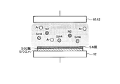
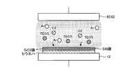
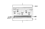
- FIGS. 5 to 11 are diagrams for explaining an example of the substrate processing performed by the substrate processing apparatus according to the first embodiment.
- the substrate processing in the substrate processing apparatus 1 is performed according to the following steps 1-1 to 1-4.
- FIG. 5 shows an example of the processing of step 1-1.
- the semiconductor wafer W to be processed is loaded into the chamber 10 with the gate valve 28 opened, and placed on the electrostatic chuck 40.
- the on / off switch 44 is turned on, and the semiconductor wafer W is suction-held on the electrostatic chuck 40 by the electrostatic suction force.
- the pressure in the chamber 10 is adjusted to a set value (for example, 500 mTorr) by the exhaust device 26.
- a heat transfer gas is supplied between the electrostatic chuck 40 and the semiconductor wafer W.
- an example of the semiconductor wafer W is a Si wafer.
- the high frequency voltage is applied to the upper electrodes 60 and 62 without applying the superimposed voltage.
- the on / off switch 92 is off, the DC pulse voltage is not supplied to the superimposing device 91, so that the DC pulse voltage is not applied to the upper electrodes 60 and 62. Further, since the substrate processing apparatus 1 adopts the configuration shown in FIG. 1, none of the high frequency voltage, the DC pulse voltage, and the superimposed voltage is applied to the susceptor 12.
- the TEOS gas, the O2 gas, and the Ar gas are introduced into the chamber 10 at predetermined flow rates as the processing gas from the gas supply unit 76.
- the Ar gas is used for stabilizing the plasma.
- the TEOS gas and the O 2 gas discharged from the inner upper electrode 60 are turned into plasma in the processing space PS by the discharge between the upper electrodes 60 and 62 and the susceptor 12 used as the lower electrode. Then, an SiO 2 film is formed on the surface of the Si wafer by radicals and ions contained in the plasma.
- the SiO 2 film is an example of an oxide film formed on the semiconductor wafer W.
- FIG. 6 shows an example of the processing of step 1-2.
- step 1-2 following step 1-1, the on / off switch 92 is turned on.
- a superimposed voltage is applied to the upper electrodes 60 and 62.
- SiH 4 gas, N 2 gas, and Ar gas are introduced into the chamber 10 at a predetermined flow rate as processing gases from the gas supply unit 76.
- the SiH4 gas and the N2 gas discharged from the inner upper electrode 60 are turned into plasma in the processing space PS by the discharge between the upper electrodes 60 and 62 and the susceptor 12 used as the lower electrode.
- a SiN film is further formed (laminated) on the surface of the SiO 2 film formed in step 1-1 by radicals and ions contained in the plasma.
- the SiN film is an example of a nitride film formed on the semiconductor wafer W.
- FIG. 7 shows an example of the processing of step 1-3.
- the on / off switch 92 is turned off.
- a high-frequency voltage is applied to the upper electrodes 60 and 62.
- TEOS gas, O 2 gas, and Ar gas are introduced into the chamber 10 at a predetermined flow rate from the gas supply unit 76 as processing gases.
- the TEOS gas and the O 2 gas discharged from the inner upper electrode 60 are turned into plasma in the processing space PS by the discharge between the upper electrodes 60 and 62 and the susceptor 12 used as the lower electrode.
- an SiO2 film is further formed (laminated) on the surface of the SiN film formed in step 1-2 by the radicals and ions contained in the plasma.
- FIG. 8 shows an example of the processing of step 1-4.
- step 1-4 following step 1-3, the on / off switch 92 is turned on.
- a superimposed voltage is applied to the upper electrodes 60 and 62.
- SiH 4 gas, N 2 gas, and Ar gas are introduced into the chamber 10 at a predetermined flow rate as processing gases from the gas supply unit 76.
- the SiH4 gas and the N2 gas discharged from the inner upper electrode 60 are turned into plasma in the processing space PS by the discharge between the upper electrodes 60 and 62 and the susceptor 12 used as the lower electrode.
- a SiN film is further formed (laminated) on the surface of the SiO 2 film formed in step 1-3 by the radicals and ions contained in the plasma.
- FIG. 10 shows the distribution of the electron temperature in the chamber 10 when the on / off switch 92 is turned off and a high frequency voltage of 40 MHz is applied to the upper electrodes 60 and 62 in a state where the pressure in the chamber 10 is set to 500 mTorr.
- FIG. 10 shows the distribution of the electron temperature in the chamber 10 when the on / off switch 92 is turned on and the superimposed voltage is applied to the upper electrodes 60 and 62 in a state where the pressure in the chamber 10 is set to 500 mTorr.
- a superimposed voltage is generated by supplying a high-frequency voltage having a frequency of 40 MHz and a DC pulse voltage having a duty ratio of 50% and a frequency of 500 kHz to the superimposing device 91.
- 9 and 10 show the relationship between the distance d in the z direction (FIG. 1) and the electron temperature (that is, the distribution of the electron temperature in the chamber 10).
- the distance d indicates a distance from the upper surface of the susceptor 12 to the lower surfaces of the upper electrodes 60 and 62, with the upper surface of the susceptor 12 (that is, the upper surface of the electrostatic chuck 40) as a base point in the z direction (FIG. 1).
- 9 and 10 show, as an example, the distribution of the electron temperature when the distance d (that is, the gap between the electrodes) between the upper surface of the susceptor 12 and the lower surfaces of the upper electrodes 60 and 62 is 0.014 m. ing.
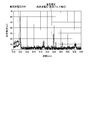
- FIG. 11 shows the relationship between the wavelength and the emission intensity when only the high-frequency voltage or the superimposed voltage is applied to the upper electrodes 60 and 62 in a state where the pressure in the chamber 10 is set to 500 mTorr.
- FIG. 9 shows a state where the processes of steps 1-1 and 1-3 (FIGS. 5 and 7) are performed, and the processes of steps 1-2 and 1-4 (FIGS. 6 and 8) are performed.
- the state at this time is shown in FIG. 10 and FIG.
- steps 1-1 and 1-3 When the processing of steps 1-1 and 1-3 is performed, that is, when a high-frequency voltage is applied to the upper electrodes 60 and 62, as shown in FIG. Both near the lower surface of 62, the electron temperature increases. As the electron temperature increases, the dissociation of the processing gas is promoted and the amount of plasma generated increases, so that the radicals contained in the plasma increase. Further, as the electron temperature is higher, the ions contained in the plasma are more activated, so that the effect of improving the film quality is improved and the film density is increased.
- radicals which are sources of the SiO 2 film
- the activity increases. Therefore, by the processing of steps 1-1 and 1-3, a SiO2 film having a high film density can be efficiently formed.
- steps 1-2 and 1-4 it is possible to form a SiN film with an increased nitriding force while suppressing damage to the susceptor 12.
- the high-frequency voltage is applied to the upper electrodes 60 and 62 without applying the DC pulse voltage to the upper electrodes 60 and 62 and the susceptor 12. Then, a process is performed on the Si wafer to form an SiO2 film on the Si wafer.
- a SiN film is formed on the Si wafer by applying a superimposed voltage to the upper electrodes 60 and 62 and performing processing on the Si wafer.
- the Si wafer is an example of a semiconductor wafer W as a substrate to be processed.
- the SiO2 film is an example of an oxide film
- the SiN film is an example of a nitride film.
- a SiO2 film can be efficiently formed while improving the film quality.
- two different film forming processes on a Si wafer can be performed in one chamber 10.
- the substrate processing apparatus 1 includes the impedance adjustment circuit 100 connected between the susceptor 12 and the ground.
- FIG. 12 is a diagram illustrating a configuration example of the substrate processing apparatus according to the second embodiment.
- the substrate processing apparatus 2 shown in FIG. 12 is configured as a capacitively coupled parallel plate substrate processing apparatus, like the substrate processing apparatus 1 (FIG. 1) according to the first embodiment.
- a configuration of the substrate processing apparatus 2 illustrated in FIG. 12 that is different from the substrate processing apparatus 1 (FIG. 1) according to the first embodiment will be described.
- the substrate processing apparatus 2 includes the voltage application unit 6.
- the voltage applying unit 6 includes the high-frequency power supply 30, an on / off switch 93, a matching unit 34, a variable DC power supply 80, an on / off switch 94, a pulse generator 84, and a filter 86.
- the high frequency power supply 30 is electrically connected to the susceptor 12 via the on / off switch 93, the matching unit 34, and the connection rod 36.
- the high-frequency power supply 30 according to the present embodiment mainly contributes to drawing ions into the semiconductor wafer W mounted on the susceptor 12.
- the matching unit 34 matches the impedance on the high-frequency power supply 30 side with the impedance on the load (mainly electrodes, plasma, chamber) side.
- the high-frequency voltage generated by the high-frequency power supply 30 is supplied to the susceptor 12 via the on / off switch 93. Therefore, when the on / off switch 93 is on, the high frequency voltage is applied to the susceptor 12, while when the on / off switch 93 is off, the high frequency voltage is applied to the susceptor 12. Not applied.
- the negative DC voltage output from the variable DC power supply 80 is supplied to the pulse generator 84 via the on / off switch 94. Therefore, when the on / off switch 94 is on, the DC pulse voltage is applied to the upper electrodes 60 and 62, while when the on / off switch 94 is off, the DC pulse voltage is applied. No voltage is applied to the upper electrodes 60,62.
- control unit (not shown).
- the operations of the exhaust device 26, the high-frequency power supply 30, the on / off changeover switches 44, 93, 94, the gas supply unit 76, the chiller unit (not shown), and the heat transfer gas supply unit (not shown) are controlled.
- Unit (not shown).
- An example of the control unit is a microcomputer.
- FIGS. 13 to 16 are views for explaining an example of the substrate processing performed by the substrate processing apparatus according to the second embodiment.
- the substrate processing in the substrate processing apparatus 2 is performed according to the following steps 2-1 to 2-3.
- FIG. 13 shows an example of the processing of step 2-1.
- the gate valve 28 is opened, and the semiconductor wafer W to be processed is carried into the chamber 10 and placed on the electrostatic chuck 40.
- the on / off switch 44 is turned on, and the semiconductor wafer W is suction-held on the electrostatic chuck 40 by the electrostatic suction force.
- the pressure in the chamber 10 is adjusted to a set value (for example, 500 mTorr) by the exhaust device 26.
- a heat transfer gas is supplied between the electrostatic chuck 40 and the semiconductor wafer W.
- an example of the semiconductor wafer W is a Si wafer.
- a natural oxide film serving as an electric resistance is attached to the surface of the Si wafer.
- An example of a natural oxide film adhering to the surface of the Si wafer is an SiO2 film.
- the high frequency voltage is applied to the susceptor 12 without applying the DC pulse voltage to the upper electrodes 60 and 62. I do.
- the substrate processing apparatus 2 adopts the configuration shown in FIG. 12, no high-frequency voltage is applied to the upper electrodes 60 and 62, and no DC pulse voltage is applied to the susceptor 12. .
- ⁇ Circle around (4) ⁇ Ar gas is introduced into the chamber 10 as a processing gas at a predetermined flow rate from the gas supply unit 76.
- the Ar gas discharged from the inner upper electrode 60 is turned into plasma in the processing space PS by a discharge between the upper electrodes 60 and 62 and the susceptor 12 used as the lower electrode. Then, ion bombardment is performed on the Si wafer by Ar ions included in the plasma, and the SiO2 film adhering to the surface of the Si wafer is washed and removed.
- FIG. 14 shows an example of the process of step 2-2.
- step 2-2 following step 2-1, the on / off switch 93 is turned off while the on / off switch 94 is turned on.
- a DC pulse voltage is applied to the upper electrodes 60 and 62 without applying a high-frequency voltage to the susceptor 12.
- TiCl 4 gas and H 2 gas are introduced into the chamber 10 at a predetermined flow rate as processing gases from the gas supply unit 76.
- the TiCl 4 gas and the H 2 gas discharged from the inner upper electrode 60 are turned into plasma in the processing space PS by discharge between the upper electrodes 60 and 62 and the susceptor 12 used as the lower electrode, and are included in the plasma.
- the radicals and ions form a Ti film on the surface of the Si wafer.
- HCl is generated when Cl of TiCl 4 is combined with H 2.
- FIG. 15 shows an example of the process of step 2-3.
- step 2-3 following step 2-2 both the on / off switch 93 and the on / off switch 94 are turned on.
- a DC pulse voltage is applied to the upper electrodes 60 and 62 while a high-frequency voltage is applied to the susceptor 12.
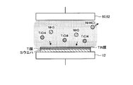
- TiCl 4 gas and NH 3 gas are introduced into the chamber 10 at a predetermined flow rate as processing gases from the gas supply unit 76.
- the TiCl 4 gas and the NH 3 gas discharged from the inner upper electrode 60 are turned into plasma in the processing space PS by the discharge between the upper electrodes 60 and 62 and the susceptor 12 used as the lower electrode, and are included in the plasma.
- the TiN film is further formed (laminated) on the surface of the Ti film formed in step 2-2 by the radicals and ions to be formed.
- the on / off switch 94 when the on / off switch 94 is turned off while the pressure in the chamber 10 is set to 500 mTorr, the on / off switch 93 is turned on, and a high-frequency voltage having a frequency of 40 MHz is applied to the susceptor 12.
- the distribution of the electron temperature in the chamber 10 is the same as that shown in FIG.
- the on / off switch 94 is turned on while the pressure in the chamber 10 is set to 500 mTorr, while the on / off switch 93 is turned off, so that the upper electrodes 60 and 62 have a duty ratio of 50% and a frequency of 500 kHz.
- FIG. 16 shows the distribution of the electron temperature in the chamber 10 when a DC pulse voltage is applied.
- both of the on / off switches 93 and 94 are turned on to apply a high frequency voltage of 40 MHz to the susceptor 12 and to apply a duty ratio to the upper electrodes 60 and 62.
- the distribution of the electron temperature in the chamber 10 when a DC pulse voltage of 50% and a frequency of 500 kHz is applied is the same as that shown in FIG.
- FIG. 16 shows an example in which the distance d between the upper surface of the susceptor 12 and the lower surfaces of the upper electrodes 60 and 62 (that is, the gap between the electrodes) is 0.014 m, as in FIGS. 9 and 10. The distribution of the electron temperature is shown.
- FIG. 9 shows a state when the processing of step 2-1 (FIG. 13) is performed
- FIG. 16 shows a state when the processing of step 2-2 (FIG. 14) is performed
- FIG. 10 and FIG. 11 show the state when the process of -3 (FIG. 15) is performed.
- step 2-1 When the process of step 2-1 is performed, that is, when a high-frequency voltage is applied to the susceptor 12, as shown in FIG. 9, both near the upper surface of the susceptor 12 and near the lower surfaces of the upper electrodes 60 and 62.
- the electron temperature increases. As the electron temperature increases, the dissociation of the processing gas is promoted and the amount of plasma generated increases, so that the number of ions contained in the plasma increases. Further, the higher the electron temperature, the more the ions contained in the plasma are activated.
- step 2-1 the Ar ions used for ion bombardment increase near the lower surfaces of the upper electrodes 60 and 62, while the activity of Ar ions contained in the plasma near the upper surface of the susceptor 12 increases. Goes up. Therefore, the cleaning effect of ion bombardment by Ar ions can be improved by the process of step 2-1.
- step 2-2 When the process of step 2-2 is performed, that is, when a DC pulse voltage is applied to the upper electrodes 60 and 62, as shown in FIG. While the electron temperature near the lower surface further increases, the electron temperature near the upper surface of the susceptor 12 drops significantly. As the electron temperature increases, the dissociation of the processing gas is promoted and the amount of plasma generated increases, so that the radicals contained in the plasma increase. Also, the lower the electron temperature, the lower the degree of damage to the electrode by ions.
- a Ti film can be efficiently formed by a large amount of radicals generated immediately below the upper electrodes 60 and 62, while suppressing damage to the susceptor 12.
- step 2-3 When the process of step 2-3 is performed, that is, when a high-frequency voltage is applied to the susceptor 12 and a DC pulse voltage is applied to the upper electrodes 60 and 62, as shown in FIG. Compared with the case of FIG. 16, the electron temperature near the upper surface of the susceptor 12 slightly increases while the electron temperature near the lower surface of the upper electrodes 60 and 62 is maintained at a high temperature similar to that in FIG. Since the electron temperature near the lower surfaces of the upper electrodes 60 and 62 is maintained at a high temperature, the dissociation of NH 3 is promoted immediately below the upper electrodes 60 and 62, as shown in FIG. Radicals increase.
- FIG. 1 When the process of step 2-3 is performed, that is, when a high-frequency voltage is applied to the susceptor 12 and a DC pulse voltage is applied to the upper electrodes 60 and 62, as shown in FIG. Compared with the case of FIG. 16, the electron temperature near the upper surface of the susceptor 12 slightly increases while the electron temperature near the lower surface of the upper electrodes
- the electron temperature in the vicinity of the upper surface of the susceptor 12 slightly increases as compared with FIG. 16, so that the processing in step 2-3 is more effective than the processing in step 2-2. Near the upper surface, the activity of ions increases.
- step 2-3 it is possible to efficiently form a TiN film having a high film density and an enhanced nitriding force.
- the high-frequency voltage is applied to the susceptor 12 without applying the DC pulse voltage to the upper electrodes 60 and 62 and the susceptor 12, and the Si wafer is processed. Is performed to clean the SiO2 film adhering to the surface of the Si wafer.
- the Si wafer is an example of a semiconductor wafer W as a substrate to be processed, and the SiO2 film is an example of a natural oxide film.
- the high frequency voltage is not applied to the upper electrodes 60 and 62 and the susceptor 12, but the DC pulse voltage is applied to the upper electrodes 60 and 62 to apply a voltage to the Si wafer. By performing the processing, a Ti film is formed on the Si wafer.
- the cleaning effect of ion bombardment can be improved.
- the Ti film can be efficiently formed while suppressing damage to the susceptor 12.
- two different processes for an Si wafer that is, an ion bombardment process and a film forming process, can be performed in one chamber 10.
- the substrate processing apparatuses 1 and 2 include the chamber 10 capable of evacuating, the susceptor 12 used as a lower electrode, and the upper electrodes 60 and 62.
- a semiconductor wafer W can be placed on the susceptor 12.
- the upper electrodes 60 and 62 are arranged in the chamber 10 so as to face the susceptor 12.
- the first processing on the semiconductor wafer W is performed using the high-frequency voltage without using the DC pulse voltage, while the second processing is performed on the semiconductor wafer W using the DC pulse voltage.
- the process of step 1-1 or the process of step 2-1 is mentioned.
- the process of step 1-2 or the process of step 2-2 can be mentioned.
Landscapes
- Chemical & Material Sciences (AREA)
- Engineering & Computer Science (AREA)
- Chemical Kinetics & Catalysis (AREA)
- Materials Engineering (AREA)
- Mechanical Engineering (AREA)
- Metallurgy (AREA)
- Organic Chemistry (AREA)
- Plasma & Fusion (AREA)
- Physics & Mathematics (AREA)
- General Chemical & Material Sciences (AREA)
- Analytical Chemistry (AREA)
- Inorganic Chemistry (AREA)
- Plasma Technology (AREA)
- Crystallography & Structural Chemistry (AREA)
- Drying Of Semiconductors (AREA)
- Formation Of Insulating Films (AREA)
- Chemical Vapour Deposition (AREA)
Abstract
Le dispositif de traitement de substrat selon la présente invention comprend : un récipient de traitement qui peut effectuer une évacuation sous vide ; une électrode inférieure ; et une électrode supérieure. Sur l'électrode inférieure, un substrat à traiter peut être placé. L'électrode supérieure est disposée dans le récipient de traitement de manière à être opposée à l'électrode inférieure. Dans le procédé de traitement de substrat selon la présente invention, un premier processus est réalisé sur un substrat à traiter à l'aide d'une tension en courant alternatif mais sans utiliser de tension d'impulsion en courant continu, tandis qu'un second processus est réalisé sur le substrat à traiter à l'aide d'une tension d'impulsion en courant continu.
Priority Applications (2)
| Application Number | Priority Date | Filing Date | Title |
|---|---|---|---|
| KR1020217001351A KR102539151B1 (ko) | 2018-06-27 | 2019-06-13 | 기판 처리 방법 |
| US17/253,789 US11410834B2 (en) | 2018-06-27 | 2019-06-13 | Substrate processing method |
Applications Claiming Priority (2)
| Application Number | Priority Date | Filing Date | Title |
|---|---|---|---|
| JP2018-122164 | 2018-06-27 | ||
| JP2018122164A JP7038614B2 (ja) | 2018-06-27 | 2018-06-27 | 基板処理方法 |
Publications (1)
| Publication Number | Publication Date |
|---|---|
| WO2020004048A1 true WO2020004048A1 (fr) | 2020-01-02 |
Family
ID=68984847
Family Applications (1)
| Application Number | Title | Priority Date | Filing Date |
|---|---|---|---|
| PCT/JP2019/023407 Ceased WO2020004048A1 (fr) | 2018-06-27 | 2019-06-13 | Procédé de traitement de substrat |
Country Status (4)
| Country | Link |
|---|---|
| US (1) | US11410834B2 (fr) |
| JP (1) | JP7038614B2 (fr) |
| KR (1) | KR102539151B1 (fr) |
| WO (1) | WO2020004048A1 (fr) |
Cited By (24)
| Publication number | Priority date | Publication date | Assignee | Title |
|---|---|---|---|---|
| US11462389B2 (en) | 2020-07-31 | 2022-10-04 | Applied Materials, Inc. | Pulsed-voltage hardware assembly for use in a plasma processing system |
| US11476090B1 (en) | 2021-08-24 | 2022-10-18 | Applied Materials, Inc. | Voltage pulse time-domain multiplexing |
| US11476145B2 (en) | 2018-11-20 | 2022-10-18 | Applied Materials, Inc. | Automatic ESC bias compensation when using pulsed DC bias |
| US11495470B1 (en) | 2021-04-16 | 2022-11-08 | Applied Materials, Inc. | Method of enhancing etching selectivity using a pulsed plasma |
| US11508554B2 (en) | 2019-01-24 | 2022-11-22 | Applied Materials, Inc. | High voltage filter assembly |
| US11569066B2 (en) | 2021-06-23 | 2023-01-31 | Applied Materials, Inc. | Pulsed voltage source for plasma processing applications |
| US11694876B2 (en) | 2021-12-08 | 2023-07-04 | Applied Materials, Inc. | Apparatus and method for delivering a plurality of waveform signals during plasma processing |
| US11699572B2 (en) | 2019-01-22 | 2023-07-11 | Applied Materials, Inc. | Feedback loop for controlling a pulsed voltage waveform |
| US11791138B2 (en) | 2021-05-12 | 2023-10-17 | Applied Materials, Inc. | Automatic electrostatic chuck bias compensation during plasma processing |
| US11798790B2 (en) | 2020-11-16 | 2023-10-24 | Applied Materials, Inc. | Apparatus and methods for controlling ion energy distribution |
| US11810760B2 (en) | 2021-06-16 | 2023-11-07 | Applied Materials, Inc. | Apparatus and method of ion current compensation |
| US11901157B2 (en) | 2020-11-16 | 2024-02-13 | Applied Materials, Inc. | Apparatus and methods for controlling ion energy distribution |
| US11948780B2 (en) | 2021-05-12 | 2024-04-02 | Applied Materials, Inc. | Automatic electrostatic chuck bias compensation during plasma processing |
| US11967483B2 (en) | 2021-06-02 | 2024-04-23 | Applied Materials, Inc. | Plasma excitation with ion energy control |
| US11972924B2 (en) | 2022-06-08 | 2024-04-30 | Applied Materials, Inc. | Pulsed voltage source for plasma processing applications |
| US11984306B2 (en) | 2021-06-09 | 2024-05-14 | Applied Materials, Inc. | Plasma chamber and chamber component cleaning methods |
| US12106938B2 (en) | 2021-09-14 | 2024-10-01 | Applied Materials, Inc. | Distortion current mitigation in a radio frequency plasma processing chamber |
| DE102023110890A1 (de) | 2023-04-27 | 2024-10-31 | Franken Systems Gmbh | 2-Komponenten-Haftprimer zur Kombination mit Flüssigkunststoffen |
| US12148595B2 (en) | 2021-06-09 | 2024-11-19 | Applied Materials, Inc. | Plasma uniformity control in pulsed DC plasma chamber |
| US12198966B2 (en) | 2017-09-20 | 2025-01-14 | Applied Materials, Inc. | Substrate support with multiple embedded electrodes |
| US12272524B2 (en) | 2022-09-19 | 2025-04-08 | Applied Materials, Inc. | Wideband variable impedance load for high volume manufacturing qualification and on-site diagnostics |
| US12315732B2 (en) | 2022-06-10 | 2025-05-27 | Applied Materials, Inc. | Method and apparatus for etching a semiconductor substrate in a plasma etch chamber |
| US12525433B2 (en) | 2021-06-09 | 2026-01-13 | Applied Materials, Inc. | Method and apparatus to reduce feature charging in plasma processing chamber |
| US12586768B2 (en) | 2022-08-10 | 2026-03-24 | Applied Materials, Inc. | Pulsed voltage compensation for plasma processing applications |
Families Citing this family (2)
| Publication number | Priority date | Publication date | Assignee | Title |
|---|---|---|---|---|
| JP2022044209A (ja) * | 2020-09-07 | 2022-03-17 | 東京エレクトロン株式会社 | プラズマ処理装置及びプラズマ処理方法 |
| KR102896679B1 (ko) * | 2022-06-20 | 2025-12-09 | 주식회사 원익아이피에스 | 적층막의 형성방법 및 이를 위한 기판 처리 장치 |
Citations (4)
| Publication number | Priority date | Publication date | Assignee | Title |
|---|---|---|---|---|
| JPH1131685A (ja) * | 1997-07-14 | 1999-02-02 | Hitachi Electron Eng Co Ltd | プラズマcvd装置およびそのクリーニング方法 |
| JP2004076069A (ja) * | 2002-08-13 | 2004-03-11 | Mitsubishi Heavy Ind Ltd | 表面処理装置 |
| JP2005026063A (ja) * | 2003-07-02 | 2005-01-27 | Sharp Corp | プラズマ処理装置およびプラズマ処理方法 |
| JP2011119720A (ja) * | 2009-11-06 | 2011-06-16 | Semiconductor Energy Lab Co Ltd | 半導体素子、及び半導体装置の作製方法、並びに成膜装置 |
Family Cites Families (3)
| Publication number | Priority date | Publication date | Assignee | Title |
|---|---|---|---|---|
| JP2009239012A (ja) | 2008-03-27 | 2009-10-15 | Tokyo Electron Ltd | プラズマ処理装置及びプラズマエッチング方法 |
| KR20160028612A (ko) * | 2014-09-03 | 2016-03-14 | 삼성전자주식회사 | 반도체 제조 장치 및 이를 이용한 반도체 소자의 제조 방법 |
| KR20170024922A (ko) * | 2015-08-26 | 2017-03-08 | 삼성전자주식회사 | 플라즈마 발생 장치 |
-
2018
- 2018-06-27 JP JP2018122164A patent/JP7038614B2/ja active Active
-
2019
- 2019-06-13 US US17/253,789 patent/US11410834B2/en active Active
- 2019-06-13 KR KR1020217001351A patent/KR102539151B1/ko active Active
- 2019-06-13 WO PCT/JP2019/023407 patent/WO2020004048A1/fr not_active Ceased
Patent Citations (4)
| Publication number | Priority date | Publication date | Assignee | Title |
|---|---|---|---|---|
| JPH1131685A (ja) * | 1997-07-14 | 1999-02-02 | Hitachi Electron Eng Co Ltd | プラズマcvd装置およびそのクリーニング方法 |
| JP2004076069A (ja) * | 2002-08-13 | 2004-03-11 | Mitsubishi Heavy Ind Ltd | 表面処理装置 |
| JP2005026063A (ja) * | 2003-07-02 | 2005-01-27 | Sharp Corp | プラズマ処理装置およびプラズマ処理方法 |
| JP2011119720A (ja) * | 2009-11-06 | 2011-06-16 | Semiconductor Energy Lab Co Ltd | 半導体素子、及び半導体装置の作製方法、並びに成膜装置 |
Cited By (38)
| Publication number | Priority date | Publication date | Assignee | Title |
|---|---|---|---|---|
| US12198966B2 (en) | 2017-09-20 | 2025-01-14 | Applied Materials, Inc. | Substrate support with multiple embedded electrodes |
| US11476145B2 (en) | 2018-11-20 | 2022-10-18 | Applied Materials, Inc. | Automatic ESC bias compensation when using pulsed DC bias |
| US12057292B2 (en) | 2019-01-22 | 2024-08-06 | Applied Materials, Inc. | Feedback loop for controlling a pulsed voltage waveform |
| US11699572B2 (en) | 2019-01-22 | 2023-07-11 | Applied Materials, Inc. | Feedback loop for controlling a pulsed voltage waveform |
| US11508554B2 (en) | 2019-01-24 | 2022-11-22 | Applied Materials, Inc. | High voltage filter assembly |
| US12237148B2 (en) | 2020-07-31 | 2025-02-25 | Applied Materials, Inc. | Plasma processing assembly using pulsed-voltage and radio-frequency power |
| US11776789B2 (en) | 2020-07-31 | 2023-10-03 | Applied Materials, Inc. | Plasma processing assembly using pulsed-voltage and radio-frequency power |
| US11462388B2 (en) | 2020-07-31 | 2022-10-04 | Applied Materials, Inc. | Plasma processing assembly using pulsed-voltage and radio-frequency power |
| US11848176B2 (en) | 2020-07-31 | 2023-12-19 | Applied Materials, Inc. | Plasma processing using pulsed-voltage and radio-frequency power |
| US11462389B2 (en) | 2020-07-31 | 2022-10-04 | Applied Materials, Inc. | Pulsed-voltage hardware assembly for use in a plasma processing system |
| US12183557B2 (en) | 2020-11-16 | 2024-12-31 | Applied Materials, Inc. | Apparatus and methods for controlling ion energy distribution |
| US11798790B2 (en) | 2020-11-16 | 2023-10-24 | Applied Materials, Inc. | Apparatus and methods for controlling ion energy distribution |
| US11901157B2 (en) | 2020-11-16 | 2024-02-13 | Applied Materials, Inc. | Apparatus and methods for controlling ion energy distribution |
| US11495470B1 (en) | 2021-04-16 | 2022-11-08 | Applied Materials, Inc. | Method of enhancing etching selectivity using a pulsed plasma |
| US11791138B2 (en) | 2021-05-12 | 2023-10-17 | Applied Materials, Inc. | Automatic electrostatic chuck bias compensation during plasma processing |
| US11948780B2 (en) | 2021-05-12 | 2024-04-02 | Applied Materials, Inc. | Automatic electrostatic chuck bias compensation during plasma processing |
| US12347647B2 (en) | 2021-06-02 | 2025-07-01 | Applied Materials, Inc. | Plasma excitation with ion energy control |
| US11967483B2 (en) | 2021-06-02 | 2024-04-23 | Applied Materials, Inc. | Plasma excitation with ion energy control |
| US12525433B2 (en) | 2021-06-09 | 2026-01-13 | Applied Materials, Inc. | Method and apparatus to reduce feature charging in plasma processing chamber |
| US11984306B2 (en) | 2021-06-09 | 2024-05-14 | Applied Materials, Inc. | Plasma chamber and chamber component cleaning methods |
| US12394596B2 (en) | 2021-06-09 | 2025-08-19 | Applied Materials, Inc. | Plasma uniformity control in pulsed DC plasma chamber |
| US12148595B2 (en) | 2021-06-09 | 2024-11-19 | Applied Materials, Inc. | Plasma uniformity control in pulsed DC plasma chamber |
| US12525441B2 (en) | 2021-06-09 | 2026-01-13 | Applied Materials, Inc. | Plasma chamber and chamber component cleaning methods |
| US11810760B2 (en) | 2021-06-16 | 2023-11-07 | Applied Materials, Inc. | Apparatus and method of ion current compensation |
| US12125673B2 (en) | 2021-06-23 | 2024-10-22 | Applied Materials, Inc. | Pulsed voltage source for plasma processing applications |
| US11887813B2 (en) | 2021-06-23 | 2024-01-30 | Applied Materials, Inc. | Pulsed voltage source for plasma processing |
| US11569066B2 (en) | 2021-06-23 | 2023-01-31 | Applied Materials, Inc. | Pulsed voltage source for plasma processing applications |
| US11476090B1 (en) | 2021-08-24 | 2022-10-18 | Applied Materials, Inc. | Voltage pulse time-domain multiplexing |
| US12261019B2 (en) | 2021-08-24 | 2025-03-25 | Applied Materials, Inc. | Voltage pulse time-domain multiplexing |
| US12106938B2 (en) | 2021-09-14 | 2024-10-01 | Applied Materials, Inc. | Distortion current mitigation in a radio frequency plasma processing chamber |
| US12482633B2 (en) | 2021-12-08 | 2025-11-25 | Applied Materials, Inc. | Apparatus and method for delivering a plurality of waveform signals during plasma processing |
| US11694876B2 (en) | 2021-12-08 | 2023-07-04 | Applied Materials, Inc. | Apparatus and method for delivering a plurality of waveform signals during plasma processing |
| US12368020B2 (en) | 2022-06-08 | 2025-07-22 | Applied Materials, Inc. | Pulsed voltage source for plasma processing applications |
| US11972924B2 (en) | 2022-06-08 | 2024-04-30 | Applied Materials, Inc. | Pulsed voltage source for plasma processing applications |
| US12315732B2 (en) | 2022-06-10 | 2025-05-27 | Applied Materials, Inc. | Method and apparatus for etching a semiconductor substrate in a plasma etch chamber |
| US12586768B2 (en) | 2022-08-10 | 2026-03-24 | Applied Materials, Inc. | Pulsed voltage compensation for plasma processing applications |
| US12272524B2 (en) | 2022-09-19 | 2025-04-08 | Applied Materials, Inc. | Wideband variable impedance load for high volume manufacturing qualification and on-site diagnostics |
| DE102023110890A1 (de) | 2023-04-27 | 2024-10-31 | Franken Systems Gmbh | 2-Komponenten-Haftprimer zur Kombination mit Flüssigkunststoffen |
Also Published As
| Publication number | Publication date |
|---|---|
| JP7038614B2 (ja) | 2022-03-18 |
| US11410834B2 (en) | 2022-08-09 |
| KR20210020134A (ko) | 2021-02-23 |
| US20210280394A1 (en) | 2021-09-09 |
| KR102539151B1 (ko) | 2023-06-01 |
| JP2020004822A (ja) | 2020-01-09 |
Similar Documents
| Publication | Publication Date | Title |
|---|---|---|
| WO2020004048A1 (fr) | Procédé de traitement de substrat | |
| WO2019239872A1 (fr) | Appareil de formation de film et procédé de nettoyage d'appareil de formation de film | |
| KR102927410B1 (ko) | 플라즈마 처리 장치 및 플라즈마 처리 방법 | |
| JP5199595B2 (ja) | プラズマ処理装置及びそのクリーニング方法 | |
| US10304691B2 (en) | Method of etching silicon oxide and silicon nitride selectively against each other | |
| US12027344B2 (en) | Film forming apparatus | |
| JP6423706B2 (ja) | プラズマ処理装置 | |
| US8641916B2 (en) | Plasma etching apparatus, plasma etching method and storage medium | |
| JP5165993B2 (ja) | プラズマ処理装置 | |
| TWI595528B (zh) | 電漿處理方法 | |
| TWI424792B (zh) | Plasma processing device and plasma processing method | |
| US20190122863A1 (en) | Plasma processing apparatus | |
| US20160372306A1 (en) | Method for Controlling Plasma Uniformity in Plasma Processing Systems | |
| WO2014057799A1 (fr) | Procédé de gravure par plasma | |
| KR20190086699A (ko) | 표면 입자를 감소시키기 위한 플라즈마 방전 점화 방법 | |
| US12020899B2 (en) | Plasma processing apparatus and plasma processing method | |
| WO2019230526A1 (fr) | Dispositif et procédé de formation de film | |
| JP6807777B2 (ja) | プラズマ処理装置 | |
| JP2007273596A (ja) | プラズマ処理用の電極板及びプラズマ処理装置 |
Legal Events
| Date | Code | Title | Description |
|---|---|---|---|
| 121 | Ep: the epo has been informed by wipo that ep was designated in this application |
Ref document number: 19825160 Country of ref document: EP Kind code of ref document: A1 |
|
| NENP | Non-entry into the national phase |
Ref country code: DE |
|
| ENP | Entry into the national phase |
Ref document number: 20217001351 Country of ref document: KR Kind code of ref document: A |
|
| 122 | Ep: pct application non-entry in european phase |
Ref document number: 19825160 Country of ref document: EP Kind code of ref document: A1 |