WO2020004048A1 - 基板処理方法 - Google Patents
基板処理方法 Download PDFInfo
- Publication number
- WO2020004048A1 WO2020004048A1 PCT/JP2019/023407 JP2019023407W WO2020004048A1 WO 2020004048 A1 WO2020004048 A1 WO 2020004048A1 JP 2019023407 W JP2019023407 W JP 2019023407W WO 2020004048 A1 WO2020004048 A1 WO 2020004048A1
- Authority
- WO
- WIPO (PCT)
- Prior art keywords
- voltage
- substrate processing
- susceptor
- chamber
- upper electrodes
- Prior art date
- Legal status (The legal status is an assumption and is not a legal conclusion. Google has not performed a legal analysis and makes no representation as to the accuracy of the status listed.)
- Ceased
Links
Images







Classifications
-
- C—CHEMISTRY; METALLURGY
- C23—COATING METALLIC MATERIAL; COATING MATERIAL WITH METALLIC MATERIAL; CHEMICAL SURFACE TREATMENT; DIFFUSION TREATMENT OF METALLIC MATERIAL; COATING BY VACUUM EVAPORATION, BY SPUTTERING, BY ION IMPLANTATION OR BY CHEMICAL VAPOUR DEPOSITION, IN GENERAL; INHIBITING CORROSION OF METALLIC MATERIAL OR INCRUSTATION IN GENERAL
- C23C—COATING METALLIC MATERIAL; COATING MATERIAL WITH METALLIC MATERIAL; SURFACE TREATMENT OF METALLIC MATERIAL BY DIFFUSION INTO THE SURFACE, BY CHEMICAL CONVERSION OR SUBSTITUTION; COATING BY VACUUM EVAPORATION, BY SPUTTERING, BY ION IMPLANTATION OR BY CHEMICAL VAPOUR DEPOSITION, IN GENERAL
- C23C16/00—Chemical coating by decomposition of gaseous compounds, without leaving reaction products of surface material in the coating, i.e. chemical vapour deposition [CVD] processes
- C23C16/22—Chemical coating by decomposition of gaseous compounds, without leaving reaction products of surface material in the coating, i.e. chemical vapour deposition [CVD] processes characterised by the deposition of inorganic material, other than metallic material
- C23C16/30—Deposition of compounds, mixtures or solid solutions, e.g. borides, carbides, nitrides
- C23C16/34—Nitrides
- C23C16/345—Silicon nitride
-
- H—ELECTRICITY
- H01—ELECTRIC ELEMENTS
- H01J—ELECTRIC DISCHARGE TUBES OR DISCHARGE LAMPS
- H01J37/00—Discharge tubes with provision for introducing objects or material to be exposed to the discharge, e.g. for the purpose of examination or processing thereof
- H01J37/32—Gas-filled discharge tubes
- H01J37/32431—Constructional details of the reactor
- H01J37/32532—Electrodes
- H01J37/32568—Relative arrangement or disposition of electrodes; moving means
-
- C—CHEMISTRY; METALLURGY
- C23—COATING METALLIC MATERIAL; COATING MATERIAL WITH METALLIC MATERIAL; CHEMICAL SURFACE TREATMENT; DIFFUSION TREATMENT OF METALLIC MATERIAL; COATING BY VACUUM EVAPORATION, BY SPUTTERING, BY ION IMPLANTATION OR BY CHEMICAL VAPOUR DEPOSITION, IN GENERAL; INHIBITING CORROSION OF METALLIC MATERIAL OR INCRUSTATION IN GENERAL
- C23C—COATING METALLIC MATERIAL; COATING MATERIAL WITH METALLIC MATERIAL; SURFACE TREATMENT OF METALLIC MATERIAL BY DIFFUSION INTO THE SURFACE, BY CHEMICAL CONVERSION OR SUBSTITUTION; COATING BY VACUUM EVAPORATION, BY SPUTTERING, BY ION IMPLANTATION OR BY CHEMICAL VAPOUR DEPOSITION, IN GENERAL
- C23C14/00—Coating by vacuum evaporation, by sputtering or by ion implantation of the coating forming material
- C23C14/06—Coating by vacuum evaporation, by sputtering or by ion implantation of the coating forming material characterised by the coating material
- C23C14/0641—Nitrides
- C23C14/0652—Silicon nitride
-
- C—CHEMISTRY; METALLURGY
- C23—COATING METALLIC MATERIAL; COATING MATERIAL WITH METALLIC MATERIAL; CHEMICAL SURFACE TREATMENT; DIFFUSION TREATMENT OF METALLIC MATERIAL; COATING BY VACUUM EVAPORATION, BY SPUTTERING, BY ION IMPLANTATION OR BY CHEMICAL VAPOUR DEPOSITION, IN GENERAL; INHIBITING CORROSION OF METALLIC MATERIAL OR INCRUSTATION IN GENERAL
- C23C—COATING METALLIC MATERIAL; COATING MATERIAL WITH METALLIC MATERIAL; SURFACE TREATMENT OF METALLIC MATERIAL BY DIFFUSION INTO THE SURFACE, BY CHEMICAL CONVERSION OR SUBSTITUTION; COATING BY VACUUM EVAPORATION, BY SPUTTERING, BY ION IMPLANTATION OR BY CHEMICAL VAPOUR DEPOSITION, IN GENERAL
- C23C14/00—Coating by vacuum evaporation, by sputtering or by ion implantation of the coating forming material
- C23C14/06—Coating by vacuum evaporation, by sputtering or by ion implantation of the coating forming material characterised by the coating material
- C23C14/10—Glass or silica
-
- C—CHEMISTRY; METALLURGY
- C23—COATING METALLIC MATERIAL; COATING MATERIAL WITH METALLIC MATERIAL; CHEMICAL SURFACE TREATMENT; DIFFUSION TREATMENT OF METALLIC MATERIAL; COATING BY VACUUM EVAPORATION, BY SPUTTERING, BY ION IMPLANTATION OR BY CHEMICAL VAPOUR DEPOSITION, IN GENERAL; INHIBITING CORROSION OF METALLIC MATERIAL OR INCRUSTATION IN GENERAL
- C23C—COATING METALLIC MATERIAL; COATING MATERIAL WITH METALLIC MATERIAL; SURFACE TREATMENT OF METALLIC MATERIAL BY DIFFUSION INTO THE SURFACE, BY CHEMICAL CONVERSION OR SUBSTITUTION; COATING BY VACUUM EVAPORATION, BY SPUTTERING, BY ION IMPLANTATION OR BY CHEMICAL VAPOUR DEPOSITION, IN GENERAL
- C23C14/00—Coating by vacuum evaporation, by sputtering or by ion implantation of the coating forming material
- C23C14/22—Coating by vacuum evaporation, by sputtering or by ion implantation of the coating forming material characterised by the process of coating
- C23C14/221—Ion beam deposition
-
- C—CHEMISTRY; METALLURGY
- C23—COATING METALLIC MATERIAL; COATING MATERIAL WITH METALLIC MATERIAL; CHEMICAL SURFACE TREATMENT; DIFFUSION TREATMENT OF METALLIC MATERIAL; COATING BY VACUUM EVAPORATION, BY SPUTTERING, BY ION IMPLANTATION OR BY CHEMICAL VAPOUR DEPOSITION, IN GENERAL; INHIBITING CORROSION OF METALLIC MATERIAL OR INCRUSTATION IN GENERAL
- C23C—COATING METALLIC MATERIAL; COATING MATERIAL WITH METALLIC MATERIAL; SURFACE TREATMENT OF METALLIC MATERIAL BY DIFFUSION INTO THE SURFACE, BY CHEMICAL CONVERSION OR SUBSTITUTION; COATING BY VACUUM EVAPORATION, BY SPUTTERING, BY ION IMPLANTATION OR BY CHEMICAL VAPOUR DEPOSITION, IN GENERAL
- C23C16/00—Chemical coating by decomposition of gaseous compounds, without leaving reaction products of surface material in the coating, i.e. chemical vapour deposition [CVD] processes
- C23C16/06—Chemical coating by decomposition of gaseous compounds, without leaving reaction products of surface material in the coating, i.e. chemical vapour deposition [CVD] processes characterised by the deposition of metallic material
-
- C—CHEMISTRY; METALLURGY
- C23—COATING METALLIC MATERIAL; COATING MATERIAL WITH METALLIC MATERIAL; CHEMICAL SURFACE TREATMENT; DIFFUSION TREATMENT OF METALLIC MATERIAL; COATING BY VACUUM EVAPORATION, BY SPUTTERING, BY ION IMPLANTATION OR BY CHEMICAL VAPOUR DEPOSITION, IN GENERAL; INHIBITING CORROSION OF METALLIC MATERIAL OR INCRUSTATION IN GENERAL
- C23C—COATING METALLIC MATERIAL; COATING MATERIAL WITH METALLIC MATERIAL; SURFACE TREATMENT OF METALLIC MATERIAL BY DIFFUSION INTO THE SURFACE, BY CHEMICAL CONVERSION OR SUBSTITUTION; COATING BY VACUUM EVAPORATION, BY SPUTTERING, BY ION IMPLANTATION OR BY CHEMICAL VAPOUR DEPOSITION, IN GENERAL
- C23C16/00—Chemical coating by decomposition of gaseous compounds, without leaving reaction products of surface material in the coating, i.e. chemical vapour deposition [CVD] processes
- C23C16/22—Chemical coating by decomposition of gaseous compounds, without leaving reaction products of surface material in the coating, i.e. chemical vapour deposition [CVD] processes characterised by the deposition of inorganic material, other than metallic material
- C23C16/30—Deposition of compounds, mixtures or solid solutions, e.g. borides, carbides, nitrides
- C23C16/40—Oxides
- C23C16/401—Oxides containing silicon
- C23C16/402—Silicon dioxide
-
- C—CHEMISTRY; METALLURGY
- C23—COATING METALLIC MATERIAL; COATING MATERIAL WITH METALLIC MATERIAL; CHEMICAL SURFACE TREATMENT; DIFFUSION TREATMENT OF METALLIC MATERIAL; COATING BY VACUUM EVAPORATION, BY SPUTTERING, BY ION IMPLANTATION OR BY CHEMICAL VAPOUR DEPOSITION, IN GENERAL; INHIBITING CORROSION OF METALLIC MATERIAL OR INCRUSTATION IN GENERAL
- C23C—COATING METALLIC MATERIAL; COATING MATERIAL WITH METALLIC MATERIAL; SURFACE TREATMENT OF METALLIC MATERIAL BY DIFFUSION INTO THE SURFACE, BY CHEMICAL CONVERSION OR SUBSTITUTION; COATING BY VACUUM EVAPORATION, BY SPUTTERING, BY ION IMPLANTATION OR BY CHEMICAL VAPOUR DEPOSITION, IN GENERAL
- C23C16/00—Chemical coating by decomposition of gaseous compounds, without leaving reaction products of surface material in the coating, i.e. chemical vapour deposition [CVD] processes
- C23C16/44—Chemical coating by decomposition of gaseous compounds, without leaving reaction products of surface material in the coating, i.e. chemical vapour deposition [CVD] processes characterised by the method of coating
- C23C16/50—Chemical coating by decomposition of gaseous compounds, without leaving reaction products of surface material in the coating, i.e. chemical vapour deposition [CVD] processes characterised by the method of coating using electric discharges
- C23C16/517—Chemical coating by decomposition of gaseous compounds, without leaving reaction products of surface material in the coating, i.e. chemical vapour deposition [CVD] processes characterised by the method of coating using electric discharges using a combination of discharges covered by two or more of groups C23C16/503 - C23C16/515
-
- H—ELECTRICITY
- H01—ELECTRIC ELEMENTS
- H01J—ELECTRIC DISCHARGE TUBES OR DISCHARGE LAMPS
- H01J37/00—Discharge tubes with provision for introducing objects or material to be exposed to the discharge, e.g. for the purpose of examination or processing thereof
- H01J37/32—Gas-filled discharge tubes
- H01J37/32009—Arrangements for generation of plasma specially adapted for examination or treatment of objects, e.g. plasma sources
- H01J37/32018—Glow discharge
- H01J37/32027—DC powered
-
- H—ELECTRICITY
- H01—ELECTRIC ELEMENTS
- H01J—ELECTRIC DISCHARGE TUBES OR DISCHARGE LAMPS
- H01J37/00—Discharge tubes with provision for introducing objects or material to be exposed to the discharge, e.g. for the purpose of examination or processing thereof
- H01J37/32—Gas-filled discharge tubes
- H01J37/32009—Arrangements for generation of plasma specially adapted for examination or treatment of objects, e.g. plasma sources
- H01J37/32018—Glow discharge
- H01J37/32045—Circuits specially adapted for controlling the glow discharge
-
- H—ELECTRICITY
- H01—ELECTRIC ELEMENTS
- H01J—ELECTRIC DISCHARGE TUBES OR DISCHARGE LAMPS
- H01J37/00—Discharge tubes with provision for introducing objects or material to be exposed to the discharge, e.g. for the purpose of examination or processing thereof
- H01J37/32—Gas-filled discharge tubes
- H01J37/32009—Arrangements for generation of plasma specially adapted for examination or treatment of objects, e.g. plasma sources
- H01J37/32082—Radio frequency generated discharge
- H01J37/32137—Radio frequency generated discharge controlling of the discharge by modulation of energy
- H01J37/32146—Amplitude modulation, includes pulsing
-
- H—ELECTRICITY
- H01—ELECTRIC ELEMENTS
- H01J—ELECTRIC DISCHARGE TUBES OR DISCHARGE LAMPS
- H01J37/00—Discharge tubes with provision for introducing objects or material to be exposed to the discharge, e.g. for the purpose of examination or processing thereof
- H01J37/32—Gas-filled discharge tubes
- H01J37/32009—Arrangements for generation of plasma specially adapted for examination or treatment of objects, e.g. plasma sources
- H01J37/32082—Radio frequency generated discharge
- H01J37/32174—Circuits specially adapted for controlling the RF discharge
-
- H—ELECTRICITY
- H01—ELECTRIC ELEMENTS
- H01J—ELECTRIC DISCHARGE TUBES OR DISCHARGE LAMPS
- H01J37/00—Discharge tubes with provision for introducing objects or material to be exposed to the discharge, e.g. for the purpose of examination or processing thereof
- H01J37/32—Gas-filled discharge tubes
- H01J37/32431—Constructional details of the reactor
- H01J37/32532—Electrodes
- H01J37/32577—Electrical connecting means
-
- H—ELECTRICITY
- H10—SEMICONDUCTOR DEVICES; ELECTRIC SOLID-STATE DEVICES NOT OTHERWISE PROVIDED FOR
- H10P—GENERIC PROCESSES OR APPARATUS FOR THE MANUFACTURE OR TREATMENT OF DEVICES COVERED BY CLASS H10
- H10P14/00—Formation of materials, e.g. in the shape of layers or pillars
- H10P14/40—Formation of materials, e.g. in the shape of layers or pillars of conductive or resistive materials
- H10P14/412—Deposition of metallic or metal-silicide materials
-
- H—ELECTRICITY
- H10—SEMICONDUCTOR DEVICES; ELECTRIC SOLID-STATE DEVICES NOT OTHERWISE PROVIDED FOR
- H10P—GENERIC PROCESSES OR APPARATUS FOR THE MANUFACTURE OR TREATMENT OF DEVICES COVERED BY CLASS H10
- H10P14/00—Formation of materials, e.g. in the shape of layers or pillars
- H10P14/40—Formation of materials, e.g. in the shape of layers or pillars of conductive or resistive materials
- H10P14/418—Formation of materials, e.g. in the shape of layers or pillars of conductive or resistive materials the conductive layers comprising transition metals
-
- H—ELECTRICITY
- H10—SEMICONDUCTOR DEVICES; ELECTRIC SOLID-STATE DEVICES NOT OTHERWISE PROVIDED FOR
- H10P—GENERIC PROCESSES OR APPARATUS FOR THE MANUFACTURE OR TREATMENT OF DEVICES COVERED BY CLASS H10
- H10P14/00—Formation of materials, e.g. in the shape of layers or pillars
- H10P14/40—Formation of materials, e.g. in the shape of layers or pillars of conductive or resistive materials
- H10P14/42—Formation of materials, e.g. in the shape of layers or pillars of conductive or resistive materials using a gas or vapour
-
- H—ELECTRICITY
- H10—SEMICONDUCTOR DEVICES; ELECTRIC SOLID-STATE DEVICES NOT OTHERWISE PROVIDED FOR
- H10P—GENERIC PROCESSES OR APPARATUS FOR THE MANUFACTURE OR TREATMENT OF DEVICES COVERED BY CLASS H10
- H10P14/00—Formation of materials, e.g. in the shape of layers or pillars
- H10P14/40—Formation of materials, e.g. in the shape of layers or pillars of conductive or resistive materials
- H10P14/42—Formation of materials, e.g. in the shape of layers or pillars of conductive or resistive materials using a gas or vapour
- H10P14/43—Chemical deposition, e.g. chemical vapour deposition [CVD]
-
- H—ELECTRICITY
- H10—SEMICONDUCTOR DEVICES; ELECTRIC SOLID-STATE DEVICES NOT OTHERWISE PROVIDED FOR
- H10P—GENERIC PROCESSES OR APPARATUS FOR THE MANUFACTURE OR TREATMENT OF DEVICES COVERED BY CLASS H10
- H10P14/00—Formation of materials, e.g. in the shape of layers or pillars
- H10P14/60—Formation of materials, e.g. in the shape of layers or pillars of insulating materials
-
- H—ELECTRICITY
- H10—SEMICONDUCTOR DEVICES; ELECTRIC SOLID-STATE DEVICES NOT OTHERWISE PROVIDED FOR
- H10P—GENERIC PROCESSES OR APPARATUS FOR THE MANUFACTURE OR TREATMENT OF DEVICES COVERED BY CLASS H10
- H10P14/00—Formation of materials, e.g. in the shape of layers or pillars
- H10P14/60—Formation of materials, e.g. in the shape of layers or pillars of insulating materials
- H10P14/63—Formation of materials, e.g. in the shape of layers or pillars of insulating materials characterised by the formation processes
- H10P14/6326—Deposition processes
- H10P14/6328—Deposition from the gas or vapour phase
- H10P14/6334—Deposition from the gas or vapour phase using decomposition or reaction of gaseous or vapour phase compounds, i.e. chemical vapour deposition
- H10P14/6336—Deposition from the gas or vapour phase using decomposition or reaction of gaseous or vapour phase compounds, i.e. chemical vapour deposition in the presence of a plasma [PECVD]
-
- H—ELECTRICITY
- H10—SEMICONDUCTOR DEVICES; ELECTRIC SOLID-STATE DEVICES NOT OTHERWISE PROVIDED FOR
- H10P—GENERIC PROCESSES OR APPARATUS FOR THE MANUFACTURE OR TREATMENT OF DEVICES COVERED BY CLASS H10
- H10P14/00—Formation of materials, e.g. in the shape of layers or pillars
- H10P14/60—Formation of materials, e.g. in the shape of layers or pillars of insulating materials
- H10P14/66—Formation of materials, e.g. in the shape of layers or pillars of insulating materials characterised by the type of materials
- H10P14/662—Laminate layers, e.g. stacks of alternating high-k metal oxides
-
- H—ELECTRICITY
- H10—SEMICONDUCTOR DEVICES; ELECTRIC SOLID-STATE DEVICES NOT OTHERWISE PROVIDED FOR
- H10P—GENERIC PROCESSES OR APPARATUS FOR THE MANUFACTURE OR TREATMENT OF DEVICES COVERED BY CLASS H10
- H10P14/00—Formation of materials, e.g. in the shape of layers or pillars
- H10P14/60—Formation of materials, e.g. in the shape of layers or pillars of insulating materials
- H10P14/69—Inorganic materials
- H10P14/692—Inorganic materials composed of oxides, glassy oxides or oxide-based glasses
- H10P14/6921—Inorganic materials composed of oxides, glassy oxides or oxide-based glasses containing silicon
- H10P14/69215—Inorganic materials composed of oxides, glassy oxides or oxide-based glasses containing silicon the material being a silicon oxide, e.g. SiO2
-
- H—ELECTRICITY
- H10—SEMICONDUCTOR DEVICES; ELECTRIC SOLID-STATE DEVICES NOT OTHERWISE PROVIDED FOR
- H10P—GENERIC PROCESSES OR APPARATUS FOR THE MANUFACTURE OR TREATMENT OF DEVICES COVERED BY CLASS H10
- H10P14/00—Formation of materials, e.g. in the shape of layers or pillars
- H10P14/60—Formation of materials, e.g. in the shape of layers or pillars of insulating materials
- H10P14/69—Inorganic materials
- H10P14/694—Inorganic materials composed of nitrides
- H10P14/6943—Inorganic materials composed of nitrides containing silicon
- H10P14/69433—Inorganic materials composed of nitrides containing silicon the material being a silicon nitride not containing oxygen, e.g. SixNy or SixByNz
-
- H—ELECTRICITY
- H10—SEMICONDUCTOR DEVICES; ELECTRIC SOLID-STATE DEVICES NOT OTHERWISE PROVIDED FOR
- H10P—GENERIC PROCESSES OR APPARATUS FOR THE MANUFACTURE OR TREATMENT OF DEVICES COVERED BY CLASS H10
- H10P50/00—Etching of wafers, substrates or parts of devices
- H10P50/20—Dry etching; Plasma etching; Reactive-ion etching
- H10P50/24—Dry etching; Plasma etching; Reactive-ion etching of semiconductor materials
- H10P50/242—Dry etching; Plasma etching; Reactive-ion etching of semiconductor materials of Group IV materials
-
- H—ELECTRICITY
- H10—SEMICONDUCTOR DEVICES; ELECTRIC SOLID-STATE DEVICES NOT OTHERWISE PROVIDED FOR
- H10P—GENERIC PROCESSES OR APPARATUS FOR THE MANUFACTURE OR TREATMENT OF DEVICES COVERED BY CLASS H10
- H10P70/00—Cleaning of wafers, substrates or parts of devices
- H10P70/20—Cleaning during device manufacture
- H10P70/27—Cleaning during device manufacture during, before or after processing of conductive materials, e.g. polysilicon or amorphous silicon layers
-
- H—ELECTRICITY
- H01—ELECTRIC ELEMENTS
- H01J—ELECTRIC DISCHARGE TUBES OR DISCHARGE LAMPS
- H01J2237/00—Discharge tubes exposing object to beam, e.g. for analysis treatment, etching, imaging
- H01J2237/32—Processing objects by plasma generation
- H01J2237/33—Processing objects by plasma generation characterised by the type of processing
- H01J2237/332—Coating
-
- H—ELECTRICITY
- H01—ELECTRIC ELEMENTS
- H01J—ELECTRIC DISCHARGE TUBES OR DISCHARGE LAMPS
- H01J37/00—Discharge tubes with provision for introducing objects or material to be exposed to the discharge, e.g. for the purpose of examination or processing thereof
- H01J37/32—Gas-filled discharge tubes
- H01J37/32009—Arrangements for generation of plasma specially adapted for examination or treatment of objects, e.g. plasma sources
- H01J37/32082—Radio frequency generated discharge
- H01J37/32091—Radio frequency generated discharge the radio frequency energy being capacitively coupled to the plasma
-
- H—ELECTRICITY
- H10—SEMICONDUCTOR DEVICES; ELECTRIC SOLID-STATE DEVICES NOT OTHERWISE PROVIDED FOR
- H10P—GENERIC PROCESSES OR APPARATUS FOR THE MANUFACTURE OR TREATMENT OF DEVICES COVERED BY CLASS H10
- H10P72/00—Handling or holding of wafers, substrates or devices during manufacture or treatment thereof
- H10P72/04—Apparatus for manufacture or treatment
- H10P72/0431—Apparatus for thermal treatment
- H10P72/0434—Apparatus for thermal treatment mainly by convection
-
- H—ELECTRICITY
- H10—SEMICONDUCTOR DEVICES; ELECTRIC SOLID-STATE DEVICES NOT OTHERWISE PROVIDED FOR
- H10P—GENERIC PROCESSES OR APPARATUS FOR THE MANUFACTURE OR TREATMENT OF DEVICES COVERED BY CLASS H10
- H10P72/00—Handling or holding of wafers, substrates or devices during manufacture or treatment thereof
- H10P72/70—Handling or holding of wafers, substrates or devices during manufacture or treatment thereof for supporting or gripping
- H10P72/72—Handling or holding of wafers, substrates or devices during manufacture or treatment thereof for supporting or gripping using electrostatic chucks
Definitions
- the present disclosure relates to a substrate processing method.
- an ion bombardment process may be performed on a semiconductor wafer before performing a film forming process on the semiconductor wafer.
- a ion bombardment treatment for example, Ar + ionized by high-frequency plasma is applied to the surface of the semiconductor wafer to destroy a natural oxide film attached to the surface of the semiconductor wafer and clean the semiconductor wafer.
- a chamber for the ion bombardment process (hereinafter, sometimes referred to as an “ion bombardment chamber”) and a chamber for the film forming process (hereinafter, “ It is necessary to prepare two chambers, which may be referred to as a “deposition chamber”.
- the transfer of the semiconductor wafer from the ion bombardment chamber to the film formation chamber has to be performed by vacuum transfer.
- the present disclosure provides a technique capable of suppressing the manufacturing cost of a semiconductor device.
- the substrate processing apparatus includes a processing container capable of evacuating, a lower electrode, and an upper electrode.
- a substrate to be processed can be placed on the lower electrode.
- the upper electrode is disposed in the processing chamber so as to face the lower electrode.
- the first processing on the target substrate is performed using the AC voltage without using the DC pulse voltage, while the second processing on the target substrate is performed using the DC pulse voltage. I do.
- the manufacturing cost of a semiconductor device can be reduced.
- FIG. 1 is a diagram illustrating a configuration example of the substrate processing apparatus according to the first embodiment.
- FIG. 2 is a diagram illustrating an example of the high-frequency voltage according to the first embodiment.
- FIG. 3 is a diagram illustrating an example of the DC pulse voltage according to the first embodiment.
- FIG. 4 is a diagram illustrating an example of a superimposed voltage according to the first embodiment.
- FIG. 5 is a view for explaining an example of the substrate processing performed by the substrate processing apparatus according to the first embodiment.
- FIG. 6 is a view for explaining an example of the substrate processing performed by the substrate processing apparatus according to the first embodiment.
- FIG. 7 is a view for explaining an example of the substrate processing performed by the substrate processing apparatus according to the first embodiment.
- FIG. 1 is a diagram illustrating a configuration example of the substrate processing apparatus according to the first embodiment.
- FIG. 2 is a diagram illustrating an example of the high-frequency voltage according to the first embodiment.
- FIG. 3 is a diagram illustrating an example of the DC pulse voltage
- FIG. 8 is a view for explaining an example of the substrate processing performed by the substrate processing apparatus according to the first embodiment.
- FIG. 9 is a view for explaining an example of the substrate processing performed by the substrate processing apparatus according to the first embodiment.
- FIG. 10 is a view for explaining an example of the substrate processing performed by the substrate processing apparatus according to the first embodiment.
- FIG. 11 is a view for explaining an example of the substrate processing performed by the substrate processing apparatus according to the first embodiment.
- FIG. 12 is a diagram illustrating a configuration example of the substrate processing apparatus according to the second embodiment.
- FIG. 13 is a view for explaining an example of the substrate processing performed by the substrate processing apparatus according to the second embodiment.
- FIG. 14 is a view for explaining an example of the substrate processing performed by the substrate processing apparatus according to the second embodiment.
- FIG. 15 is a view for explaining an example of the substrate processing performed by the substrate processing apparatus according to the second embodiment.
- FIG. 16 is a diagram for explaining an example of the substrate processing performed by the substrate processing apparatus according to the second
- FIG. 1 is a diagram illustrating a configuration example of the substrate processing apparatus according to the first embodiment.
- the substrate processing apparatus 1 shown in FIG. 1 is configured as a capacitively coupled parallel plate substrate processing apparatus.
- the substrate processing apparatus 1 includes a chamber 10 which is a metal processing container made of, for example, aluminum or stainless steel.
- the chamber 10 is grounded for security.
- a disk-shaped susceptor 12 is horizontally arranged.
- a semiconductor wafer W as a substrate to be processed for substrate processing can be placed.
- the susceptor 12 also functions as a lower electrode.
- a gate valve 28 for opening and closing the loading / unloading port of the semiconductor wafer W is attached to a side wall of the chamber 10.
- the susceptor 12 is made of, for example, AlN ceramic, and is supported by an insulating tubular support 14 extending vertically upward from the bottom of the chamber 10.
- An annular exhaust passage 18 is formed between a conductive cylindrical support (inner wall) 16 extending vertically upward from the bottom of the chamber 10 along the outer periphery of the cylindrical support 14 and a side wall of the chamber 10. I have.
- An exhaust port 22 is provided at the bottom of the exhaust path 18.
- An exhaust device 26 is connected to the exhaust port 22 via an exhaust pipe 24.
- the exhaust device 26 has a vacuum pump such as a turbo-molecular pump, for example, and reduces the pressure in the processing space in the chamber 10 to a desired degree of vacuum.
- the inside of the chamber 10 is preferably maintained at a constant pressure in a range of, for example, 200 mTorr to 2500 mTorr.
- An impedance adjustment circuit 100 having a coil 101 and a variable capacitor 102 is electrically connected via a connecting rod 36 between the susceptor 12 used as a lower electrode and the ground.
- a semiconductor wafer W to be processed is placed on the susceptor 12, and a ring 38 is provided so as to surround the semiconductor wafer W.
- the ring 38 is made of a conductive material (for example, Ni, Al, or the like), and is detachably attached to the upper surface of the susceptor 12.
- an electrostatic chuck 40 for sucking a wafer is provided on the upper surface of the susceptor 12.
- the electrostatic chuck 40 is formed by sandwiching a sheet-shaped or mesh-shaped conductor between film-shaped or plate-shaped dielectrics.
- a DC power source 42 disposed outside the chamber 10 is electrically connected to a conductor in the electrostatic chuck 40 via an on / off switch 44 and a power supply line 46.
- the semiconductor wafer W is suction-held on the electrostatic chuck 40 by the Coulomb force generated in the electrostatic chuck 40 by the DC voltage applied from the DC power supply 42.
- a circular refrigerant chamber 48 extending in the circumferential direction is provided inside the susceptor 12.
- a coolant for example, cooling water
- the chiller unit (not shown) to the coolant chamber 48 via pipes 50 and 52.
- a heat transfer gas for example, He gas
- a heat transfer gas supply unit passes through the gas supply pipe 51 and the gas passage 56 in the susceptor 12. Then, it is supplied between the electrostatic chuck 40 and the semiconductor wafer W.
- a disc-shaped inner upper electrode 60 and a ring-shaped outer upper electrode 62 are provided concentrically on the ceiling of the chamber 10 so as to face (ie, face) the susceptor 12 in parallel.
- the inner upper electrode 60 has a diameter (diameter) similar to the semiconductor wafer W
- the outer upper electrode 62 has a diameter (inner diameter / outer diameter) similar to the ring 38. I have.
- the inner upper electrode 60 and the outer upper electrode 62 are electrically insulated from each other.
- a ring-shaped insulator 63 made of, for example, ceramic is inserted between the two electrodes 60 and 62.
- the inner upper electrode 60 has an electrode plate 64 facing directly in front of the susceptor 12, and an electrode support 66 for detachably supporting the electrode plate 64 from behind (above).
- a material of the electrode plate 64 a conductive material such as Ni or Al is preferable.
- the electrode support 66 is made of, for example, anodized aluminum.
- the outer upper electrode 62 also has an electrode plate 68 facing the susceptor 12 and an electrode support 70 for detachably supporting the electrode plate 68 from behind (from above).
- the electrode plate 68 and the electrode support 70 are preferably made of the same material as the electrode plate 64 and the electrode support 66, respectively.
- the inner upper electrode 60 and the outer upper electrode 62 may be collectively referred to as “upper electrodes 60, 62”.
- the disc-shaped susceptor 12 that is, the lower electrode
- the disc-shaped upper electrodes 60 and 62 face each other in parallel.
- the upper electrode may be composed of one member.
- the inner upper electrode 60 is also used as a shower head to supply a processing gas to the processing space PS set between the upper electrodes 60 and 62 and the susceptor 12. More specifically, a gas diffusion chamber 72 is provided inside the electrode support 66, and a number of gas discharge holes 74 penetrating from the gas diffusion chamber 72 to the susceptor 12 are formed in the electrode support 66 and the electrode plate 64. A gas supply pipe 78 extending from a gas supply unit 76 is connected to a gas inlet 72 a provided at an upper portion of the gas diffusion chamber 72.
- the shower head may be provided not only on the inner upper electrode 60 but also on the outer upper electrode 62.
- a voltage applying unit 5 for outputting an applied voltage is arranged outside the chamber 10.
- the voltage applying unit 5 is connected to the upper electrodes 60 and 62 via a power supply line 88.
- the voltage applying unit 5 includes a high-frequency power supply 30, a matching unit 34, a variable DC power supply 80, an on / off switch 92, a pulse generator 84, a filter 86, and a superposition unit 91.
- the high-frequency power supply 30 generates a high-frequency AC voltage (hereinafter sometimes referred to as a “high-frequency voltage”), and supplies the generated high-frequency voltage to the superimposing device 91 via the matching unit 34.
- the frequency of the high-frequency voltage generated by the high-frequency power supply 30 is preferably, for example, 13 MHz or more.
- FIG. 2 is a diagram illustrating an example of the high-frequency voltage according to the first embodiment.
- the high-frequency power supply 30 generates a high-frequency voltage V1 of ⁇ 250 V to 250 V with 0 V as a reference potential RP, for example.
- the matching unit 34 matches the impedance on the high-frequency power supply 30 side with the impedance on the load (mainly electrodes, plasma, chamber) side.
- the output terminal of the variable DC power supply 80 is connected to a pulse generator 84 via an on / off switch 92, and the variable DC power supply 80 outputs a negative DC voltage (that is, a negative DC voltage) to the pulse generator 84.
- a negative DC voltage is input to the pulse generator 84
- the on / off switch 92 is off
- the negative DC voltage is input. Is not input to the pulse generator 84.
- the pulse generator 84 generates a square-wave DC pulse voltage (that is, a DC pulse voltage) using a negative DC voltage input from the variable DC power supply 80, and superimposes the generated DC pulse voltage via a filter 86.
- the frequency of the DC pulse voltage generated by the pulse generator 84 is preferably, for example, 10 kHz to 1 MHz.
- the duty ratio of the DC pulse voltage generated by the pulse generator 84 is preferably 10% to 90%.
- FIG. 3 is a diagram illustrating an example of the DC pulse voltage according to the first embodiment.
- the pulse generator 84 generates a DC pulse voltage V2 of, for example, a rectangular wave of 0V to -500V.
- the filter 86 outputs the DC pulse voltage output from the pulse generator 84 to the superimposing device 91 in a through manner, while flowing the high frequency voltage output from the high frequency power supply 30 to the ground line and to the pulse generator 84 side. Not configured.
- the superimposer 91 superimposes the high-frequency voltage output from the high-frequency power supply 30 and the DC pulse voltage output from the pulse generator 84 to thereby superimpose the high-frequency voltage and the DC pulse voltage (hereinafter, “voltage”). Superimposed voltage). The generated superimposed voltage is applied to the upper electrodes 60 and 62 via the power supply line 88.
- FIG. 4 is a diagram illustrating an example of the superimposed voltage according to the first embodiment.
- a superimposed voltage V3 shown in FIG. 4 is generated.
- the high-frequency voltage V1 (FIG. 2) matches the waveform of the rectangular DC pulse voltage V2 (FIG. 2).
- the reference potential RP alternately changes vertically with time over time. That is, when the on / off switch 92 is on, the voltage applying unit 5 outputs a high-frequency voltage that changes in a pulse shape (that is, a rectangular wave shape).
- the on / off switch 92 when the on / off switch 92 is turned on, the negative DC voltage output from the variable DC power supply 80 is supplied to the pulse generator 84. Is output. On the other hand, when the on / off switch 92 is off, the negative DC voltage output from the variable DC power supply 80 is not supplied to the pulse generator 84, so that the high-frequency voltage output from the matching unit 34 is It is output from the superimposing device 91 as it is.
- the on / off switch 92 when the on / off switch 92 is on, the superimposed voltage is applied to the upper electrodes 60 and 62, while when the on / off switch 92 is off, the high frequency voltage is The voltage is applied to the upper electrodes 60 and 62.
- a ring-shaped ground part 96 made of a conductive material such as Ni or Al is attached to an appropriate position facing the processing space PS in the chamber 10 (for example, radially outside the outer upper electrode 62). .
- the ground part 96 is attached to a ring-shaped insulator 98 made of, for example, ceramic, is connected to a ceiling wall of the chamber 10, and is grounded via the chamber 10.
- a superimposed voltage or a DC pulse voltage is applied from the voltage applying unit 5 to the upper electrodes 60 and 62 during the plasma processing, an electron current flows between the upper electrodes 60 and 62 and the ground part 96 via the plasma. Has become.
- control unit The individual operation of each component in the substrate processing apparatus 1 and the operation (sequence) of the entire substrate processing apparatus 1 are controlled by a control unit (not shown).
- the operations of the exhaust device 26, the high-frequency power supply 30, the on / off changeover switches 44 and 92, the gas supply unit 76, the chiller unit (not shown), the heat transfer gas supply unit (not shown), and the like are controlled by the control unit ( (Not shown).
- An example of the control unit is a microcomputer.
- FIGS. 5 to 11 are diagrams for explaining an example of the substrate processing performed by the substrate processing apparatus according to the first embodiment.
- the substrate processing in the substrate processing apparatus 1 is performed according to the following steps 1-1 to 1-4.
- FIG. 5 shows an example of the processing of step 1-1.
- the semiconductor wafer W to be processed is loaded into the chamber 10 with the gate valve 28 opened, and placed on the electrostatic chuck 40.
- the on / off switch 44 is turned on, and the semiconductor wafer W is suction-held on the electrostatic chuck 40 by the electrostatic suction force.
- the pressure in the chamber 10 is adjusted to a set value (for example, 500 mTorr) by the exhaust device 26.
- a heat transfer gas is supplied between the electrostatic chuck 40 and the semiconductor wafer W.
- an example of the semiconductor wafer W is a Si wafer.
- the high frequency voltage is applied to the upper electrodes 60 and 62 without applying the superimposed voltage.
- the on / off switch 92 is off, the DC pulse voltage is not supplied to the superimposing device 91, so that the DC pulse voltage is not applied to the upper electrodes 60 and 62. Further, since the substrate processing apparatus 1 adopts the configuration shown in FIG. 1, none of the high frequency voltage, the DC pulse voltage, and the superimposed voltage is applied to the susceptor 12.
- the TEOS gas, the O2 gas, and the Ar gas are introduced into the chamber 10 at predetermined flow rates as the processing gas from the gas supply unit 76.
- the Ar gas is used for stabilizing the plasma.
- the TEOS gas and the O 2 gas discharged from the inner upper electrode 60 are turned into plasma in the processing space PS by the discharge between the upper electrodes 60 and 62 and the susceptor 12 used as the lower electrode. Then, an SiO 2 film is formed on the surface of the Si wafer by radicals and ions contained in the plasma.
- the SiO 2 film is an example of an oxide film formed on the semiconductor wafer W.
- FIG. 6 shows an example of the processing of step 1-2.
- step 1-2 following step 1-1, the on / off switch 92 is turned on.
- a superimposed voltage is applied to the upper electrodes 60 and 62.
- SiH 4 gas, N 2 gas, and Ar gas are introduced into the chamber 10 at a predetermined flow rate as processing gases from the gas supply unit 76.
- the SiH4 gas and the N2 gas discharged from the inner upper electrode 60 are turned into plasma in the processing space PS by the discharge between the upper electrodes 60 and 62 and the susceptor 12 used as the lower electrode.
- a SiN film is further formed (laminated) on the surface of the SiO 2 film formed in step 1-1 by radicals and ions contained in the plasma.
- the SiN film is an example of a nitride film formed on the semiconductor wafer W.
- FIG. 7 shows an example of the processing of step 1-3.
- the on / off switch 92 is turned off.
- a high-frequency voltage is applied to the upper electrodes 60 and 62.
- TEOS gas, O 2 gas, and Ar gas are introduced into the chamber 10 at a predetermined flow rate from the gas supply unit 76 as processing gases.
- the TEOS gas and the O 2 gas discharged from the inner upper electrode 60 are turned into plasma in the processing space PS by the discharge between the upper electrodes 60 and 62 and the susceptor 12 used as the lower electrode.
- an SiO2 film is further formed (laminated) on the surface of the SiN film formed in step 1-2 by the radicals and ions contained in the plasma.
- FIG. 8 shows an example of the processing of step 1-4.
- step 1-4 following step 1-3, the on / off switch 92 is turned on.
- a superimposed voltage is applied to the upper electrodes 60 and 62.
- SiH 4 gas, N 2 gas, and Ar gas are introduced into the chamber 10 at a predetermined flow rate as processing gases from the gas supply unit 76.
- the SiH4 gas and the N2 gas discharged from the inner upper electrode 60 are turned into plasma in the processing space PS by the discharge between the upper electrodes 60 and 62 and the susceptor 12 used as the lower electrode.
- a SiN film is further formed (laminated) on the surface of the SiO 2 film formed in step 1-3 by the radicals and ions contained in the plasma.
- FIG. 10 shows the distribution of the electron temperature in the chamber 10 when the on / off switch 92 is turned off and a high frequency voltage of 40 MHz is applied to the upper electrodes 60 and 62 in a state where the pressure in the chamber 10 is set to 500 mTorr.
- FIG. 10 shows the distribution of the electron temperature in the chamber 10 when the on / off switch 92 is turned on and the superimposed voltage is applied to the upper electrodes 60 and 62 in a state where the pressure in the chamber 10 is set to 500 mTorr.
- a superimposed voltage is generated by supplying a high-frequency voltage having a frequency of 40 MHz and a DC pulse voltage having a duty ratio of 50% and a frequency of 500 kHz to the superimposing device 91.
- 9 and 10 show the relationship between the distance d in the z direction (FIG. 1) and the electron temperature (that is, the distribution of the electron temperature in the chamber 10).
- the distance d indicates a distance from the upper surface of the susceptor 12 to the lower surfaces of the upper electrodes 60 and 62, with the upper surface of the susceptor 12 (that is, the upper surface of the electrostatic chuck 40) as a base point in the z direction (FIG. 1).
- 9 and 10 show, as an example, the distribution of the electron temperature when the distance d (that is, the gap between the electrodes) between the upper surface of the susceptor 12 and the lower surfaces of the upper electrodes 60 and 62 is 0.014 m. ing.
- FIG. 11 shows the relationship between the wavelength and the emission intensity when only the high-frequency voltage or the superimposed voltage is applied to the upper electrodes 60 and 62 in a state where the pressure in the chamber 10 is set to 500 mTorr.
- FIG. 9 shows a state where the processes of steps 1-1 and 1-3 (FIGS. 5 and 7) are performed, and the processes of steps 1-2 and 1-4 (FIGS. 6 and 8) are performed.
- the state at this time is shown in FIG. 10 and FIG.
- steps 1-1 and 1-3 When the processing of steps 1-1 and 1-3 is performed, that is, when a high-frequency voltage is applied to the upper electrodes 60 and 62, as shown in FIG. Both near the lower surface of 62, the electron temperature increases. As the electron temperature increases, the dissociation of the processing gas is promoted and the amount of plasma generated increases, so that the radicals contained in the plasma increase. Further, as the electron temperature is higher, the ions contained in the plasma are more activated, so that the effect of improving the film quality is improved and the film density is increased.
- radicals which are sources of the SiO 2 film
- the activity increases. Therefore, by the processing of steps 1-1 and 1-3, a SiO2 film having a high film density can be efficiently formed.
- steps 1-2 and 1-4 it is possible to form a SiN film with an increased nitriding force while suppressing damage to the susceptor 12.
- the high-frequency voltage is applied to the upper electrodes 60 and 62 without applying the DC pulse voltage to the upper electrodes 60 and 62 and the susceptor 12. Then, a process is performed on the Si wafer to form an SiO2 film on the Si wafer.
- a SiN film is formed on the Si wafer by applying a superimposed voltage to the upper electrodes 60 and 62 and performing processing on the Si wafer.
- the Si wafer is an example of a semiconductor wafer W as a substrate to be processed.
- the SiO2 film is an example of an oxide film
- the SiN film is an example of a nitride film.
- a SiO2 film can be efficiently formed while improving the film quality.
- two different film forming processes on a Si wafer can be performed in one chamber 10.
- the substrate processing apparatus 1 includes the impedance adjustment circuit 100 connected between the susceptor 12 and the ground.
- FIG. 12 is a diagram illustrating a configuration example of the substrate processing apparatus according to the second embodiment.
- the substrate processing apparatus 2 shown in FIG. 12 is configured as a capacitively coupled parallel plate substrate processing apparatus, like the substrate processing apparatus 1 (FIG. 1) according to the first embodiment.
- a configuration of the substrate processing apparatus 2 illustrated in FIG. 12 that is different from the substrate processing apparatus 1 (FIG. 1) according to the first embodiment will be described.
- the substrate processing apparatus 2 includes the voltage application unit 6.
- the voltage applying unit 6 includes the high-frequency power supply 30, an on / off switch 93, a matching unit 34, a variable DC power supply 80, an on / off switch 94, a pulse generator 84, and a filter 86.
- the high frequency power supply 30 is electrically connected to the susceptor 12 via the on / off switch 93, the matching unit 34, and the connection rod 36.
- the high-frequency power supply 30 according to the present embodiment mainly contributes to drawing ions into the semiconductor wafer W mounted on the susceptor 12.
- the matching unit 34 matches the impedance on the high-frequency power supply 30 side with the impedance on the load (mainly electrodes, plasma, chamber) side.
- the high-frequency voltage generated by the high-frequency power supply 30 is supplied to the susceptor 12 via the on / off switch 93. Therefore, when the on / off switch 93 is on, the high frequency voltage is applied to the susceptor 12, while when the on / off switch 93 is off, the high frequency voltage is applied to the susceptor 12. Not applied.
- the negative DC voltage output from the variable DC power supply 80 is supplied to the pulse generator 84 via the on / off switch 94. Therefore, when the on / off switch 94 is on, the DC pulse voltage is applied to the upper electrodes 60 and 62, while when the on / off switch 94 is off, the DC pulse voltage is applied. No voltage is applied to the upper electrodes 60,62.
- control unit (not shown).
- the operations of the exhaust device 26, the high-frequency power supply 30, the on / off changeover switches 44, 93, 94, the gas supply unit 76, the chiller unit (not shown), and the heat transfer gas supply unit (not shown) are controlled.
- Unit (not shown).
- An example of the control unit is a microcomputer.
- FIGS. 13 to 16 are views for explaining an example of the substrate processing performed by the substrate processing apparatus according to the second embodiment.
- the substrate processing in the substrate processing apparatus 2 is performed according to the following steps 2-1 to 2-3.
- FIG. 13 shows an example of the processing of step 2-1.
- the gate valve 28 is opened, and the semiconductor wafer W to be processed is carried into the chamber 10 and placed on the electrostatic chuck 40.
- the on / off switch 44 is turned on, and the semiconductor wafer W is suction-held on the electrostatic chuck 40 by the electrostatic suction force.
- the pressure in the chamber 10 is adjusted to a set value (for example, 500 mTorr) by the exhaust device 26.
- a heat transfer gas is supplied between the electrostatic chuck 40 and the semiconductor wafer W.
- an example of the semiconductor wafer W is a Si wafer.
- a natural oxide film serving as an electric resistance is attached to the surface of the Si wafer.
- An example of a natural oxide film adhering to the surface of the Si wafer is an SiO2 film.
- the high frequency voltage is applied to the susceptor 12 without applying the DC pulse voltage to the upper electrodes 60 and 62. I do.
- the substrate processing apparatus 2 adopts the configuration shown in FIG. 12, no high-frequency voltage is applied to the upper electrodes 60 and 62, and no DC pulse voltage is applied to the susceptor 12. .
- ⁇ Circle around (4) ⁇ Ar gas is introduced into the chamber 10 as a processing gas at a predetermined flow rate from the gas supply unit 76.
- the Ar gas discharged from the inner upper electrode 60 is turned into plasma in the processing space PS by a discharge between the upper electrodes 60 and 62 and the susceptor 12 used as the lower electrode. Then, ion bombardment is performed on the Si wafer by Ar ions included in the plasma, and the SiO2 film adhering to the surface of the Si wafer is washed and removed.
- FIG. 14 shows an example of the process of step 2-2.
- step 2-2 following step 2-1, the on / off switch 93 is turned off while the on / off switch 94 is turned on.
- a DC pulse voltage is applied to the upper electrodes 60 and 62 without applying a high-frequency voltage to the susceptor 12.
- TiCl 4 gas and H 2 gas are introduced into the chamber 10 at a predetermined flow rate as processing gases from the gas supply unit 76.
- the TiCl 4 gas and the H 2 gas discharged from the inner upper electrode 60 are turned into plasma in the processing space PS by discharge between the upper electrodes 60 and 62 and the susceptor 12 used as the lower electrode, and are included in the plasma.
- the radicals and ions form a Ti film on the surface of the Si wafer.
- HCl is generated when Cl of TiCl 4 is combined with H 2.
- FIG. 15 shows an example of the process of step 2-3.
- step 2-3 following step 2-2 both the on / off switch 93 and the on / off switch 94 are turned on.
- a DC pulse voltage is applied to the upper electrodes 60 and 62 while a high-frequency voltage is applied to the susceptor 12.
- TiCl 4 gas and NH 3 gas are introduced into the chamber 10 at a predetermined flow rate as processing gases from the gas supply unit 76.
- the TiCl 4 gas and the NH 3 gas discharged from the inner upper electrode 60 are turned into plasma in the processing space PS by the discharge between the upper electrodes 60 and 62 and the susceptor 12 used as the lower electrode, and are included in the plasma.
- the TiN film is further formed (laminated) on the surface of the Ti film formed in step 2-2 by the radicals and ions to be formed.
- the on / off switch 94 when the on / off switch 94 is turned off while the pressure in the chamber 10 is set to 500 mTorr, the on / off switch 93 is turned on, and a high-frequency voltage having a frequency of 40 MHz is applied to the susceptor 12.
- the distribution of the electron temperature in the chamber 10 is the same as that shown in FIG.
- the on / off switch 94 is turned on while the pressure in the chamber 10 is set to 500 mTorr, while the on / off switch 93 is turned off, so that the upper electrodes 60 and 62 have a duty ratio of 50% and a frequency of 500 kHz.
- FIG. 16 shows the distribution of the electron temperature in the chamber 10 when a DC pulse voltage is applied.
- both of the on / off switches 93 and 94 are turned on to apply a high frequency voltage of 40 MHz to the susceptor 12 and to apply a duty ratio to the upper electrodes 60 and 62.
- the distribution of the electron temperature in the chamber 10 when a DC pulse voltage of 50% and a frequency of 500 kHz is applied is the same as that shown in FIG.
- FIG. 16 shows an example in which the distance d between the upper surface of the susceptor 12 and the lower surfaces of the upper electrodes 60 and 62 (that is, the gap between the electrodes) is 0.014 m, as in FIGS. 9 and 10. The distribution of the electron temperature is shown.
- FIG. 9 shows a state when the processing of step 2-1 (FIG. 13) is performed
- FIG. 16 shows a state when the processing of step 2-2 (FIG. 14) is performed
- FIG. 10 and FIG. 11 show the state when the process of -3 (FIG. 15) is performed.
- step 2-1 When the process of step 2-1 is performed, that is, when a high-frequency voltage is applied to the susceptor 12, as shown in FIG. 9, both near the upper surface of the susceptor 12 and near the lower surfaces of the upper electrodes 60 and 62.
- the electron temperature increases. As the electron temperature increases, the dissociation of the processing gas is promoted and the amount of plasma generated increases, so that the number of ions contained in the plasma increases. Further, the higher the electron temperature, the more the ions contained in the plasma are activated.
- step 2-1 the Ar ions used for ion bombardment increase near the lower surfaces of the upper electrodes 60 and 62, while the activity of Ar ions contained in the plasma near the upper surface of the susceptor 12 increases. Goes up. Therefore, the cleaning effect of ion bombardment by Ar ions can be improved by the process of step 2-1.
- step 2-2 When the process of step 2-2 is performed, that is, when a DC pulse voltage is applied to the upper electrodes 60 and 62, as shown in FIG. While the electron temperature near the lower surface further increases, the electron temperature near the upper surface of the susceptor 12 drops significantly. As the electron temperature increases, the dissociation of the processing gas is promoted and the amount of plasma generated increases, so that the radicals contained in the plasma increase. Also, the lower the electron temperature, the lower the degree of damage to the electrode by ions.
- a Ti film can be efficiently formed by a large amount of radicals generated immediately below the upper electrodes 60 and 62, while suppressing damage to the susceptor 12.
- step 2-3 When the process of step 2-3 is performed, that is, when a high-frequency voltage is applied to the susceptor 12 and a DC pulse voltage is applied to the upper electrodes 60 and 62, as shown in FIG. Compared with the case of FIG. 16, the electron temperature near the upper surface of the susceptor 12 slightly increases while the electron temperature near the lower surface of the upper electrodes 60 and 62 is maintained at a high temperature similar to that in FIG. Since the electron temperature near the lower surfaces of the upper electrodes 60 and 62 is maintained at a high temperature, the dissociation of NH 3 is promoted immediately below the upper electrodes 60 and 62, as shown in FIG. Radicals increase.
- FIG. 1 When the process of step 2-3 is performed, that is, when a high-frequency voltage is applied to the susceptor 12 and a DC pulse voltage is applied to the upper electrodes 60 and 62, as shown in FIG. Compared with the case of FIG. 16, the electron temperature near the upper surface of the susceptor 12 slightly increases while the electron temperature near the lower surface of the upper electrodes
- the electron temperature in the vicinity of the upper surface of the susceptor 12 slightly increases as compared with FIG. 16, so that the processing in step 2-3 is more effective than the processing in step 2-2. Near the upper surface, the activity of ions increases.
- step 2-3 it is possible to efficiently form a TiN film having a high film density and an enhanced nitriding force.
- the high-frequency voltage is applied to the susceptor 12 without applying the DC pulse voltage to the upper electrodes 60 and 62 and the susceptor 12, and the Si wafer is processed. Is performed to clean the SiO2 film adhering to the surface of the Si wafer.
- the Si wafer is an example of a semiconductor wafer W as a substrate to be processed, and the SiO2 film is an example of a natural oxide film.
- the high frequency voltage is not applied to the upper electrodes 60 and 62 and the susceptor 12, but the DC pulse voltage is applied to the upper electrodes 60 and 62 to apply a voltage to the Si wafer. By performing the processing, a Ti film is formed on the Si wafer.
- the cleaning effect of ion bombardment can be improved.
- the Ti film can be efficiently formed while suppressing damage to the susceptor 12.
- two different processes for an Si wafer that is, an ion bombardment process and a film forming process, can be performed in one chamber 10.
- the substrate processing apparatuses 1 and 2 include the chamber 10 capable of evacuating, the susceptor 12 used as a lower electrode, and the upper electrodes 60 and 62.
- a semiconductor wafer W can be placed on the susceptor 12.
- the upper electrodes 60 and 62 are arranged in the chamber 10 so as to face the susceptor 12.
- the first processing on the semiconductor wafer W is performed using the high-frequency voltage without using the DC pulse voltage, while the second processing is performed on the semiconductor wafer W using the DC pulse voltage.
- the process of step 1-1 or the process of step 2-1 is mentioned.
- the process of step 1-2 or the process of step 2-2 can be mentioned.
Landscapes
- Chemical & Material Sciences (AREA)
- Engineering & Computer Science (AREA)
- Chemical Kinetics & Catalysis (AREA)
- Materials Engineering (AREA)
- Mechanical Engineering (AREA)
- Metallurgy (AREA)
- Organic Chemistry (AREA)
- Plasma & Fusion (AREA)
- Physics & Mathematics (AREA)
- General Chemical & Material Sciences (AREA)
- Analytical Chemistry (AREA)
- Inorganic Chemistry (AREA)
- Plasma Technology (AREA)
- Crystallography & Structural Chemistry (AREA)
- Chemical Vapour Deposition (AREA)
- Drying Of Semiconductors (AREA)
- Formation Of Insulating Films (AREA)
Abstract
本開示の基板処理装置は、真空排気可能な処理容器と、下部電極と、上部電極とを有する。下部電極には被処理基板が載置可能である。上部電極は、処理容器内で下部電極に対向して配置される。そして、本開示の基板処理方法では、直流パルス電圧を用いずに交流電圧を用いて被処理基板に対する第一処理を行う一方で、直流パルス電圧を用いて被処理基板に対する第二処理を行う。
Description
本開示は、基板処理方法に関する。
半導体デバイスの製造工程において、半導体ウエハに対して成膜処理を行う前に、半導体ウエハに対してイオンボンバードメント処理を行うことがある。イオンボンバードメント処理では、例えば高周波プラズマでイオン化されたAr+を半導体ウエハの表面にたたきつけることにより、半導体ウエハの表面に付着した自然酸化膜を破壊して洗浄する。
成膜処理を行う前にイオンボンバードメント処理を行うには、イオンボンバードメント処理用のチャンバ(以下では「イオンボンバードメントチャンバ」と呼ぶことがある)と、成膜処理用のチャンバ(以下では「成膜チャンバ」と呼ぶことがある)という、2つのチャンバを用意する必要があった。
また、イオンボンバードメント処理後の半導体ウエハを、イオンボンバードメントチャンバから成膜チャンバへと空気中で搬送すると、イオンボンバードメントにより除去された自然酸化膜が空気中で再び半導体ウエハに付着してしまう。このため、イオンボンバードメントチャンバから成膜チャンバへの半導体ウエハの搬送は、真空搬送にて行う必要があった。
それぞれ別用途の2つのチャンバを用意すると、半導体デバイスの製造コストが高くなってしまう。また、半導体ウエハを真空搬送するには真空搬送用の別装置が必要になるため、半導体ウエハの真空搬送を行うと、半導体デバイスの製造コストがさらに高くなってしまう。
本開示は、半導体デバイスの製造コストを抑えることができる技術を提供する。
本開示の一態様の基板処理装置は、真空排気可能な処理容器と、下部電極と、上部電極とを有する。下部電極には被処理基板が載置可能である。上部電極は、処理容器内で下部電極に対向して配置される。そして、本開示の一態様の基板処理方法では、直流パルス電圧を用いずに交流電圧を用いて被処理基板に対する第一処理を行う一方で、直流パルス電圧を用いて被処理基板に対する第二処理を行う。
本開示の技術によれば、半導体デバイスの製造コストを抑えることができる。
以下に、本開示の技術の実施形態を図面に基づいて説明する。各実施形態において同一の構成には同一の符号を付すことにより、実施形態間で重複する説明は省略する。
[実施形態1]
<基板処理装置の構成>
図1は、実施形態1に係る基板処理装置の構成例を示す図である。図1に示す基板処理装置1は、容量結合型の平行平板基板処理装置として構成されている。
<基板処理装置の構成>
図1は、実施形態1に係る基板処理装置の構成例を示す図である。図1に示す基板処理装置1は、容量結合型の平行平板基板処理装置として構成されている。
図1において、基板処理装置1は、例えばアルミニウムまたはステンレス鋼等からなる金属製の処理容器であるチャンバ10を有する。チャンバ10は保安接地されている。
チャンバ10内には、円盤状のサセプタ12が水平に配置されている。サセプタ12には、基板処理の被処理基板としての半導体ウエハWが載置可能である。サセプタ12は、下部電極としても機能する。チャンバ10の側壁には、半導体ウエハWの搬入出口を開閉するゲートバルブ28が取り付けられている。サセプタ12は、例えばAlNセラミック等からなり、チャンバ10の底から鉛直上方に延びる絶縁性の筒状支持部14に支持されている。
筒状支持部14の外周に沿ってチャンバ10の底から鉛直上方に延びる導電性の筒状支持部(内壁部)16とチャンバ10の側壁との間に、環状の排気路18が形成されている。排気路18の底には排気口22が設けられている。
排気口22には排気管24を介して排気装置26が接続されている。排気装置26は、例えばターボ分子ポンプ等の真空ポンプを有しており、チャンバ10内の処理空間を所望の真空度まで減圧する。チャンバ10内は、例えば、200mTorr~2500mTorrの範囲の一定の圧力に保たれるのが好ましい。
下部電極として用いられるサセプタ12と接地との間には、コイル101と可変コンデンサ102とを有するインピーダンス調整回路100が接続棒36を介して電気的に接続されている。
サセプタ12の上には基板処理対象の半導体ウエハWが載置され、半導体ウエハWを囲むようにリング38が設けられている。リング38は、導電材(例えばNi,Al等)からなり、サセプタ12の上面に着脱可能に取り付けられる。
また、サセプタ12の上面には、ウエハ吸着用の静電チャック40が設けられている。静電チャック40は、膜状または板状の誘電体の間にシート状またはメッシュ状の導電体を挟んで形成される。静電チャック40内の導電体には、チャンバ10の外に配置される直流電源42がオン/オフ切替スイッチ44及び給電線46を介して電気的に接続されている。直流電源42より印加される直流電圧によって静電チャック40に発生したクーロン力により、半導体ウエハWが静電チャック40上に吸着保持される。
サセプタ12の内部には、円周方向に延びる環状の冷媒室48が設けられている。冷媒室48には、チラーユニット(図示せず)より配管50,52を介して、所定温度の冷媒(例えば冷却水)が循環供給される。冷媒の温度を制御することによって静電チャック40上の半導体ウエハWの温度が制御される。さらに、半導体ウエハWの温度の精度を高めるために、伝熱ガス供給部(図示せず)からの伝熱ガス(例えばHeガス)が、ガス供給管51及びサセプタ12内のガス通路56を介して、静電チャック40と半導体ウエハWとの間に供給される。
チャンバ10の天井には、サセプタ12と平行に向かい合って(つまり、対向して)、円盤状の内側上部電極60及びリング状の外側上部電極62が同心状に設けられている。径方向の好適なサイズとして、内側上部電極60は半導体ウエハWと同程度の口径(直径)を有し、外側上部電極62はリング38と同程度の口径(内径・外径)を有している。但し、内側上部電極60と外側上部電極62とは互いに電気的に絶縁されている。両電極60,62の間には、例えばセラミックからなるリング状の絶縁体63が挿入されている。
内側上部電極60は、サセプタ12と真正面に向かい合う電極板64と、電極板64をその背後(上)から着脱可能に支持する電極支持体66とを有している。電極板64の材質として、NiまたはAl等の導電材が好ましい。電極支持体66は、例えばアルマイト処理されたアルミニウムで構成される。外側上部電極62も、サセプタ12と向かい合う電極板68と、電極板68をその背後(上)から着脱可能に支持する電極支持体70とを有している。電極板68及び電極支持体70は、電極板64及び電極支持体66とそれぞれ同じ材質で構成されるのが好ましい。以下では、内側上部電極60と外側上部電極62とを「上部電極60,62」と総称することがある。このように、基板処理装置1では、円盤状のサセプタ12(つまり、下部電極)と、円盤状の上部電極60,62とが互いに平行に対向している。
なお、本実施形態では、上部電極60,62が、内側上部電極60と外側上部電極62との2つの部材で構成される場合を一例として挙げた。しかし、上部電極は1つの部材で構成されても良い。
上部電極60,62とサセプタ12との間に設定される処理空間PSに処理ガスを供給するために、内側上部電極60がシャワーヘッドとして兼用される。より詳細には、電極支持体66の内部にガス拡散室72が設けられ、ガス拡散室72からサセプタ12側に貫ける多数のガス吐出孔74が電極支持体66及び電極板64に形成される。ガス拡散室72の上部に設けられるガス導入口72aには、ガス供給部76から延びるガス供給管78が接続されている。なお、内側上部電極60だけでなく外側上部電極62にもシャワーヘッドを設ける構成としても良い。
チャンバ10の外には、印加電圧を出力する電圧印加部5が配置されている。電圧印加部5は、給電ライン88を介して上部電極60,62に接続されている。電圧印加部5は、高周波電源30と、マッチングユニット34と、可変直流電源80と、オン/オフ切替スイッチ92と、パルス発生器84と、フィルタ86と、重畳器91とを有する。
高周波電源30は、高周波数の交流電圧(以下では「高周波電圧」と呼ぶことがある)を生成し、生成した高周波電圧をマッチングユニット34を介して重畳器91に供給する。高周波電源30が生成する高周波電圧の周波数は、例えば13MHz以上であることが好ましい。
図2は、実施形態1に係る高周波電圧の一例を示す図である。図2に示すように、高周波電源30は、例えば、0Vを基準電位RPとする-250V~250Vの高周波電圧V1を生成する。マッチングユニット34は、高周波電源30側のインピーダンスと負荷(主に電極、プラズマ、チャンバ)側のインピーダンスとの間の整合をとる。
可変直流電源80の出力端子はオン/オフ切替スイッチ92を介してパルス発生器84に接続され、可変直流電源80は、負の直流電圧(つまり負のDC電圧)をパルス発生器84に出力する。オン/オフ切替スイッチ92がオンになっているときは、負の直流電圧がパルス発生器84に入力される一方で、オン/オフ切替スイッチ92がオフになっているときは、負の直流電圧がパルス発生器84に入力されない。パルス発生器84は、可変直流電源80から入力される負の直流電圧を用いて、矩形波の直流パルス電圧(つまりDCパルス電圧)を発生し、発生した直流パルス電圧をフィルタ86を介して重畳器91に供給する。パルス発生器84が発生する直流パルス電圧の周波数は、例えば、10kHz~1MHzであることが好ましい。また、パルス発生器84が発生する直流パルス電圧のデューティ比は、10%~90%であることが好ましい。
図3は、実施形態1に係る直流パルス電圧の一例を示す図である。図3に示すように、パルス発生器84は、例えば、0V~-500Vの矩形波の直流パルス電圧V2を生成する。
フィルタ86は、パルス発生器84から出力される直流パルス電圧をスルーで重畳器91へ出力する一方で、高周波電源30から出力される高周波電圧を接地ラインへ流してパルス発生器84側へは流さないように構成されている。
重畳器91は、高周波電源30から出力される高周波電圧と、パルス発生器84から出力される直流パルス電圧とを重畳することにより、高周波電圧と直流パルス電圧とが重畳された電圧(以下では「重畳電圧」と呼ぶことがある)を生成する。生成された重畳電圧は、給電ライン88を介して上部電極60,62に印加される。
図4は、実施形態1に係る重畳電圧の一例を示す図である。図2示す高周波電圧V1と図3に示す直流パルス電圧V2とが重畳された場合、図4に示す重畳電圧V3が生成される。高周波電圧に直流パルス電圧が重畳されることにより、図4に示すように、重畳電圧V3においては、矩形波の直流パルス電圧V2(図3)の波形に合わせて、高周波電圧V1(図2)の基準電位RPが時間の経過に伴って上下に交互に周期的に変化する。つまり、電圧印加部5は、オン/オフ切替スイッチ92がオンになっている場合には、パルス状(つまり、矩形波状)に変化する高周波電圧を出力する。
このように、オン/オフ切替スイッチ92がオンになっているときは、可変直流電源80から出力される負の直流電圧がパルス発生器84に供給されるので、重畳器91からは重畳電圧が出力される。一方で、オン/オフ切替スイッチ92がオフになっているときは、可変直流電源80から出力される負の直流電圧がパルス発生器84に供給されないので、マッチングユニット34から出力された高周波電圧がそのまま重畳器91から出力される。
つまり、オン/オフ切替スイッチ92がオンになっているときは、重畳電圧が上部電極60,62に印加される一方で、オン/オフ切替スイッチ92がオフになっているときは、高周波電圧が上部電極60,62に印加される。
チャンバ10内で処理空間PSに面する適当な箇所(例えば、外側上部電極62の半径方向外側)には、例えばNi,Al等の導電性部材からなるリング状のグランドパーツ96が取り付けられている。グランドパーツ96は、例えばセラミックからなるリング状の絶縁体98に取り付けられるとともに、チャンバ10の天井壁に接続されており、チャンバ10を介して接地されている。プラズマ処理中に電圧印加部5から上部電極60,62に重畳電圧または直流パルス電圧が印加されると、プラズマを介して上部電極60,62とグランドパーツ96との間で電子電流が流れるようになっている。
基板処理装置1内の各構成の個々の動作、及び、基板処理装置1全体の動作(シーケンス)は、制御部(図示せず)によって制御される。例えば、排気装置26、高周波電源30、オン/オフ切替スイッチ44,92、ガス供給部76、チラーユニット(図示せず)、伝熱ガス供給部(図示せず)等の動作は、制御部(図示せず)によって制御される。制御部の一例として、マイクロコンピュータが挙げられる。
<基板処理装置での基板処理>
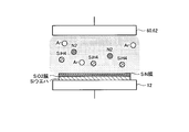
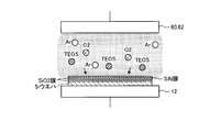
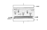
図5~図11は、実施形態1に係る基板処理装置で行われる基板処理の一例の説明に供する図である。基板処理装置1における基板処理は、以下のステップ1-1~1-4に従って行われる。
図5~図11は、実施形態1に係る基板処理装置で行われる基板処理の一例の説明に供する図である。基板処理装置1における基板処理は、以下のステップ1-1~1-4に従って行われる。
<ステップ1-1:図5>
図5にステップ1-1の処理の一例を示す。基板処理装置1において、まずゲートバルブ28を開状態にして加工対象の半導体ウエハWをチャンバ10内に搬入して、静電チャック40の上に載置する。次に、オン/オフ切替スイッチ44をオンにし、静電吸着力によって静電チャック40上に半導体ウエハWを吸着保持する。また、排気装置26によりチャンバ10内の圧力を設定値(例えば、500mTorr)に調節する。また、静電チャック40と半導体ウエハWとの間に伝熱ガスを供給する。図5に示すように、半導体ウエハWの一例として、Siウエハが挙げられる。
図5にステップ1-1の処理の一例を示す。基板処理装置1において、まずゲートバルブ28を開状態にして加工対象の半導体ウエハWをチャンバ10内に搬入して、静電チャック40の上に載置する。次に、オン/オフ切替スイッチ44をオンにし、静電吸着力によって静電チャック40上に半導体ウエハWを吸着保持する。また、排気装置26によりチャンバ10内の圧力を設定値(例えば、500mTorr)に調節する。また、静電チャック40と半導体ウエハWとの間に伝熱ガスを供給する。図5に示すように、半導体ウエハWの一例として、Siウエハが挙げられる。
また、オン/オフ切替スイッチ92をオフにすることにより、上部電極60,62には、重畳電圧を印加せずに高周波電圧を印加する。オン/オフ切替スイッチ92がオフになっているときは、直流パルス電圧は重畳器91に供給されないため、直流パルス電圧は上部電極60,62にも印加されない。また、基板処理装置1が図1に示す構成を採ることにより、サセプタ12には、高周波電圧、直流パルス電圧及び重畳電圧の何れも印加されることはない。
また、ガス供給部76より処理ガスとして、TEOSガス、O2ガス及びArガスを所定の流量でチャンバ10内に導入する。なお、Arガスは、プラズマの安定化のために用いられる。
これにより、内側上部電極60より吐出されたTEOSガス及びO2ガスは、上部電極60,62と、下部電極として用いられるサセプタ12との間での放電によって処理空間PSでプラズマ化する。そして、このプラズマに含まれるラジカルやイオンによって、Siウエハの表面にSiO2膜が形成される。SiO2膜は、半導体ウエハW上に形成される酸化膜の一例である。
<ステップ1-2:図6>
図6にステップ1-2の処理の一例を示す。ステップ1-1に後続するステップ1-2では、オン/オフ切替スイッチ92をオンにする。オン/オフ切替スイッチ92をオンにすることにより、上部電極60,62には、重畳電圧が印加される。また、ガス供給部76より処理ガスとして、SiH4ガス、N2ガス及びArガスを所定の流量でチャンバ10内に導入する。これにより、内側上部電極60より吐出されたSiH4ガス及びN2ガスは、上部電極60,62と、下部電極として用いられるサセプタ12との間での放電によって処理空間PSでプラズマ化する。そして、このプラズマに含まれるラジカルやイオンによって、ステップ1-1で形成されたSiO2膜の表面にさらにSiN膜が形成(積層)される。SiN膜は、半導体ウエハW上に形成される窒化膜の一例である。
図6にステップ1-2の処理の一例を示す。ステップ1-1に後続するステップ1-2では、オン/オフ切替スイッチ92をオンにする。オン/オフ切替スイッチ92をオンにすることにより、上部電極60,62には、重畳電圧が印加される。また、ガス供給部76より処理ガスとして、SiH4ガス、N2ガス及びArガスを所定の流量でチャンバ10内に導入する。これにより、内側上部電極60より吐出されたSiH4ガス及びN2ガスは、上部電極60,62と、下部電極として用いられるサセプタ12との間での放電によって処理空間PSでプラズマ化する。そして、このプラズマに含まれるラジカルやイオンによって、ステップ1-1で形成されたSiO2膜の表面にさらにSiN膜が形成(積層)される。SiN膜は、半導体ウエハW上に形成される窒化膜の一例である。
<ステップ1-3:図7>
図7にステップ1-3の処理の一例を示す。ステップ1-2に後続するステップ1-3では、オン/オフ切替スイッチ92をオフにする。オン/オフ切替スイッチ92をオフにすることにより、上部電極60,62には、高周波電圧が印加される。また、ガス供給部76より処理ガスとして、TEOSガス、O2ガス及びArガスを所定の流量でチャンバ10内に導入する。これにより、内側上部電極60より吐出されたTEOSガス及びO2ガスは、上部電極60,62と、下部電極として用いられるサセプタ12との間での放電によって処理空間PSでプラズマ化する。そして、このプラズマに含まれるラジカルやイオンによって、ステップ1-2で形成されたSiN膜の表面にさらにSiO2膜が形成(積層)される。
図7にステップ1-3の処理の一例を示す。ステップ1-2に後続するステップ1-3では、オン/オフ切替スイッチ92をオフにする。オン/オフ切替スイッチ92をオフにすることにより、上部電極60,62には、高周波電圧が印加される。また、ガス供給部76より処理ガスとして、TEOSガス、O2ガス及びArガスを所定の流量でチャンバ10内に導入する。これにより、内側上部電極60より吐出されたTEOSガス及びO2ガスは、上部電極60,62と、下部電極として用いられるサセプタ12との間での放電によって処理空間PSでプラズマ化する。そして、このプラズマに含まれるラジカルやイオンによって、ステップ1-2で形成されたSiN膜の表面にさらにSiO2膜が形成(積層)される。
<ステップ1-4:図8>
図8にステップ1-4の処理の一例を示す。ステップ1-3に後続するステップ1-4では、オン/オフ切替スイッチ92をオンにする。オン/オフ切替スイッチ92をオンにすることにより、上部電極60,62には、重畳電圧が印加される。また、ガス供給部76より処理ガスとして、SiH4ガス、N2ガス及びArガスを所定の流量でチャンバ10内に導入する。これにより、内側上部電極60より吐出されたSiH4ガス及びN2ガスは、上部電極60,62と、下部電極として用いられるサセプタ12との間での放電によって処理空間PSでプラズマ化する。そして、このプラズマに含まれるラジカルやイオンによって、ステップ1-3で形成されたSiO2膜の表面にさらにSiN膜が形成(積層)される。
図8にステップ1-4の処理の一例を示す。ステップ1-3に後続するステップ1-4では、オン/オフ切替スイッチ92をオンにする。オン/オフ切替スイッチ92をオンにすることにより、上部電極60,62には、重畳電圧が印加される。また、ガス供給部76より処理ガスとして、SiH4ガス、N2ガス及びArガスを所定の流量でチャンバ10内に導入する。これにより、内側上部電極60より吐出されたSiH4ガス及びN2ガスは、上部電極60,62と、下部電極として用いられるサセプタ12との間での放電によって処理空間PSでプラズマ化する。そして、このプラズマに含まれるラジカルやイオンによって、ステップ1-3で形成されたSiO2膜の表面にさらにSiN膜が形成(積層)される。
以上、ステップ1-1~1-4の処理について説明した。
ここで、チャンバ10内の圧力を500mTorrにした状態でオン/オフ切替スイッチ92をオフにして上部電極60,62に周波数40MHzの高周波電圧を印加したときのチャンバ10内の電子温度の分布を図9に示す。また、チャンバ10内の圧力を500mTorrにした状態でオン/オフ切替スイッチ92をオンにして上部電極60,62に重畳電圧を印加したときのチャンバ10内の電子温度の分布を図10に示す。図10では、周波数40MHzの高周波電圧、及び、デューティ比50%、周波数500kHzの直流パルス電圧を重畳器91に供給することにより重畳電圧を生成した。図9及び図10は、z方向(図1)の距離dと電子温度との関係(つまり、チャンバ10内の電子温度の分布)を示す。距離dは、z方向(図1)において、サセプタ12の上面(つまり、静電チャック40の上面)を基点とし、サセプタ12の上面から上部電極60,62の下面までの距離を示す。図9及び図10では、一例として、サセプタ12の上面と上部電極60,62の下面との間の距離d(つまり、電極間ギャップ)が0.014mである場合の電子温度の分布が示されている。
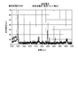
また、図11に、チャンバ10内の圧力を500mTorrにした状態で上部電極60,62に高周波電圧のみ、または、重畳電圧を印加したときの波長と発光強度との関係を示す。
つまり、ステップ1-1,1-3(図5,7)の処理が行われるときの状態が図9に示され、ステップ1-2,1-4(図6,8)の処理が行われるときの状態が図10及び図11に示されている。
ステップ1-1,1-3の処理が行われるとき、つまり、上部電極60,62に高周波電圧が印加されるときには、図9に示すように、サセプタ12の上面付近、及び、上部電極60,62の下面付近の双方で、電子温度が高くなる。電子温度が高いほど、処理ガスの解離が促進されてプラズマの生成量が増加するため、プラズマに含まれるラジカルが増加する。また、電子温度が高いほど、プラズマに含まれるイオンがより活性化されるため、膜質の改善効果が上がって膜密度が上がる。
よって、ステップ1-1,1-3の処理により、上部電極60,62の下面付近では、SiO2膜の形成源であるラジカルが増加する一方で、サセプタ12の上面付近では、プラズマに含まれるイオンの活性度が上がる。よって、ステップ1-1,1-3の処理により、膜密度が高いSiO2膜を効率良く形成することができる。
これに対し、ステップ1-2,1-4の処理が行われるとき、つまり、上部電極60,62に重畳電圧が印加されるときには、図10に示すように、図9と比較して、上部電極60,62の下面付近での電子温度がさらに上昇する一方で、サセプタ12の上面付近での電子温度が大きく低下する。上部電極60,62の下面付近での電子温度の上昇により、図11に示すように、上部電極60,62の直下においてN2の解離が促進されて、SiN膜の形成源であるNラジカルが増加する。図11からは、上部電極60,62に重畳電圧を印加した場合は、高周波電圧のみを印加した場合に比べ、N2の発光強度が減少する一方で、N2の解離が促進されてNラジカルの発光強度が増加していること(つまり、Nラジカルが増加していること)が分かる。よって、上部電極60,62に重畳電圧を印加することにより、ステップ1-2,1-4の処理で形成されるSiN膜での窒化力を強化することができる。
一方で、電子温度が低いほど、イオンによる電極に対する損傷の度合が小さくなる。
よって、ステップ1-2,1-4の処理により、サセプタ12に対する損傷を抑制しつつ、窒化力が強化されたSiN膜を形成することができる。
以上のように、実施形態1では、ステップ1-1,1-3の処理において、直流パルス電圧を上部電極60,62及びサセプタ12に印加せずに、高周波電圧を上部電極60,62に印加してSiウエハに対する処理を行うことにより、Siウエハ上にSiO2膜を形成する。また、実施形態1では、ステップ1-2,1-4の処理において、重畳電圧を上部電極60,62に印加してSiウエハに対する処理を行うことにより、Siウエハ上にSiN膜を形成する。Siウエハは、被処理基板としての半導体ウエハWの一例である。また、SiO2膜は酸化膜の一例であり、SiN膜は窒化膜の一例である。
こうすることで、ステップ1-1,1-3の処理では、膜質を改善しながらSiO2膜を効率良く形成することができる。一方で、ステップ1-2,1-4の処理では、サセプタ12に対する損傷を抑制しつつ、窒化力が強化されたSiN膜を形成することができる。このように、実施形態1によれば、Siウエハに対する互いに異なる2つの成膜処理を1つのチャンバ10内で行うことができる。
また、実施形態1では、基板処理装置1は、サセプタ12と接地との間に接続されたインピーダンス調整回路100を有する。
こうすることで、上部電極60,62とサセプタ12との間のインピーダンスを減少させることが可能になるため、上部電極60,62に印加される高周波電圧、及び、上部電極60,62に印加される重畳電圧の高周波電圧成分がサセプタ12に到達し易くなる。
[実施形態2]
<基板処理装置の構成>
図12は、実施形態2に係る基板処理装置の構成例を示す図である。図12に示す基板処理装置2は、実施形態1に係る基板処理装置1(図1)と同様に、容量結合型の平行平板基板処理装置として構成されている。以下、図12に示す基板処理装置2において、実施形態1に係る基板処理装置1(図1)と異なる構成について説明する。
<基板処理装置の構成>
図12は、実施形態2に係る基板処理装置の構成例を示す図である。図12に示す基板処理装置2は、実施形態1に係る基板処理装置1(図1)と同様に、容量結合型の平行平板基板処理装置として構成されている。以下、図12に示す基板処理装置2において、実施形態1に係る基板処理装置1(図1)と異なる構成について説明する。
基板処理装置2は、電圧印加部6を有する。電圧印加部6は、高周波電源30と、オン/オフ切替スイッチ93と、マッチングユニット34と、可変直流電源80と、オン/オフ切替スイッチ94と、パルス発生器84と、フィルタ86とを有する。
高周波電源30は、オン/オフ切替スイッチ93、マッチングユニット34及び接続棒36を介して、サセプタ12に電気的に接続されている。本実施形態の高周波電源30は、主に、サセプタ12上に載置される半導体ウエハWに対するイオンの引き込みに寄与する。マッチングユニット34は、高周波電源30側のインピーダンスと負荷(主に電極、プラズマ、チャンバ)側のインピーダンスとの間の整合をとる。高周波電源30によって生成された高周波電圧は、オン/オフ切替スイッチ93を介してサセプタ12に供給される。よって、オン/オフ切替スイッチ93がオンになっているときは、高周波電圧がサセプタ12に印加される一方で、オン/オフ切替スイッチ93がオフになっているときは、高周波電圧がサセプタ12に印加されない。
一方で、可変直流電源80から出力される負の直流電圧はオン/オフ切替スイッチ94を介してパルス発生器84に供給される。よって、オン/オフ切替スイッチ94がオンになっているときは、直流パルス電圧が上部電極60,62に印加される一方で、オン/オフ切替スイッチ94がオフになっているときは、直流パルス電圧が上部電極60,62に印加されない。
基板処理装置2内の各構成の個々の動作、及び、基板処理装置2全体の動作(シーケンス)は、制御部(図示せず)によって制御される。例えば、排気装置26、高周波電源30、オン/オフ切替スイッチ44,93,94、ガス供給部76、チラーユニット(図示せず)、伝熱ガス供給部(図示せず)等の動作は、制御部(図示せず)によって制御される。制御部の一例として、マイクロコンピュータが挙げられる。
<基板処理装置での基板処理>
図13~図16は、実施形態2に係る基板処理装置で行われる基板処理の一例の説明に供する図である。基板処理装置2における基板処理は、以下のステップ2-1~2-3に従って行われる。
図13~図16は、実施形態2に係る基板処理装置で行われる基板処理の一例の説明に供する図である。基板処理装置2における基板処理は、以下のステップ2-1~2-3に従って行われる。
<ステップ2-1:図13>
図13にステップ2-1の処理の一例を示す。基板処理装置2において、まずゲートバルブ28を開状態にして加工対象の半導体ウエハWをチャンバ10内に搬入して、静電チャック40の上に載置する。次に、オン/オフ切替スイッチ44をオンにし、静電吸着力によって静電チャック40上に半導体ウエハWを吸着保持する。また、排気装置26によりチャンバ10内の圧力を設定値(例えば、500mTorr)に調節する。また、静電チャック40と半導体ウエハWとの間に伝熱ガスを供給する。図13に示すように、半導体ウエハWの一例として、Siウエハが挙げられる。このSiウエハの表面には、電気抵抗になる自然酸化膜が付着している。Siウエハの表面に付着している自然酸化膜の一例として、SiO2膜が挙げられる。
図13にステップ2-1の処理の一例を示す。基板処理装置2において、まずゲートバルブ28を開状態にして加工対象の半導体ウエハWをチャンバ10内に搬入して、静電チャック40の上に載置する。次に、オン/オフ切替スイッチ44をオンにし、静電吸着力によって静電チャック40上に半導体ウエハWを吸着保持する。また、排気装置26によりチャンバ10内の圧力を設定値(例えば、500mTorr)に調節する。また、静電チャック40と半導体ウエハWとの間に伝熱ガスを供給する。図13に示すように、半導体ウエハWの一例として、Siウエハが挙げられる。このSiウエハの表面には、電気抵抗になる自然酸化膜が付着している。Siウエハの表面に付着している自然酸化膜の一例として、SiO2膜が挙げられる。
また、オン/オフ切替スイッチ94をオフにする一方で、オン/オフ切替スイッチ93をオンにすることにより、上部電極60,62に直流パルス電圧を印加せずに、サセプタ12に高周波電圧を印加する。また、基板処理装置2が図12に示す構成を採ることにより、上部電極60,62には高周波電圧が印加されることはなく、また、サセプタ12には直流パルス電圧が印加されることはない。
また、ガス供給部76より処理ガスとしてArガスを所定の流量でチャンバ10内に導入する。
これにより、内側上部電極60より吐出されたArガスは、上部電極60,62と、下部電極として用いられるサセプタ12との間での放電によって処理空間PSでプラズマ化する。そして、このプラズマに含まれるArイオンによってSiウエハに対してイオンボンバードメントが行われて、Siウエハの表面に付着しているSiO2膜が洗浄されて除去される。
<ステップ2-2:図14>
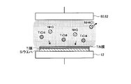
図14にステップ2-2の処理の一例を示す。ステップ2-1に後続するステップ2-2では、オン/オフ切替スイッチ93をオフにする一方で、オン/オフ切替スイッチ94をオンにする。これにより、サセプタ12に高周波電圧が印加されずに、上部電極60,62に直流パルス電圧が印加される。また、ガス供給部76より処理ガスとして、TiCl4ガス及びH2ガスを所定の流量でチャンバ10内に導入する。これにより、内側上部電極60より吐出されたTiCl4ガス及びH2ガスは、上部電極60,62と、下部電極として用いられるサセプタ12との間での放電によって処理空間PSでプラズマ化し、このプラズマに含まれるラジカルやイオンによって、Siウエハの表面にTi膜が形成される。また、TiCl4のClとH2とが結びつくことによりHClが生成される。
図14にステップ2-2の処理の一例を示す。ステップ2-1に後続するステップ2-2では、オン/オフ切替スイッチ93をオフにする一方で、オン/オフ切替スイッチ94をオンにする。これにより、サセプタ12に高周波電圧が印加されずに、上部電極60,62に直流パルス電圧が印加される。また、ガス供給部76より処理ガスとして、TiCl4ガス及びH2ガスを所定の流量でチャンバ10内に導入する。これにより、内側上部電極60より吐出されたTiCl4ガス及びH2ガスは、上部電極60,62と、下部電極として用いられるサセプタ12との間での放電によって処理空間PSでプラズマ化し、このプラズマに含まれるラジカルやイオンによって、Siウエハの表面にTi膜が形成される。また、TiCl4のClとH2とが結びつくことによりHClが生成される。
<ステップ2-3:図15>
図15にステップ2-3の処理の一例を示す。ステップ2-2に後続するステップ2-3では、オン/オフ切替スイッチ93及びオン/オフ切替スイッチ94の双方をオンにする。これにより、サセプタ12に高周波電圧が印加される一方で、上部電極60,62に直流パルス電圧が印加される。また、ガス供給部76より処理ガスとして、TiCl4ガス及びNH3ガスを所定の流量でチャンバ10内に導入する。これにより、内側上部電極60より吐出されたTiCl4ガス及びNH3ガスは、上部電極60,62と、下部電極として用いられるサセプタ12との間での放電によって処理空間PSでプラズマ化し、このプラズマに含まれるラジカルやイオンによって、ステップ2-2で形成されたTi膜の表面にさらにTiN膜が形成(積層)される。
図15にステップ2-3の処理の一例を示す。ステップ2-2に後続するステップ2-3では、オン/オフ切替スイッチ93及びオン/オフ切替スイッチ94の双方をオンにする。これにより、サセプタ12に高周波電圧が印加される一方で、上部電極60,62に直流パルス電圧が印加される。また、ガス供給部76より処理ガスとして、TiCl4ガス及びNH3ガスを所定の流量でチャンバ10内に導入する。これにより、内側上部電極60より吐出されたTiCl4ガス及びNH3ガスは、上部電極60,62と、下部電極として用いられるサセプタ12との間での放電によって処理空間PSでプラズマ化し、このプラズマに含まれるラジカルやイオンによって、ステップ2-2で形成されたTi膜の表面にさらにTiN膜が形成(積層)される。
以上、ステップ2-1~2-3の処理について説明した。
ここで、チャンバ10内の圧力を500mTorrにした状態でオン/オフ切替スイッチ94をオフにする一方でオン/オフ切替スイッチ93をオンにして、サセプタ12に周波数40MHzの高周波電圧を印加したときのチャンバ10内の電子温度の分布は、上記の図9に示したものと同様になる。また、チャンバ10内の圧力を500mTorrにした状態でオン/オフ切替スイッチ94をオンにする一方でオン/オフ切替スイッチ93をオフにして、上部電極60,62にデューティ比50%、周波数500kHzの直流パルス電圧を印加したときのチャンバ10内の電子温度の分布を図16に示す。また、チャンバ10内の圧力を500mTorrにした状態でオン/オフ切替スイッチ93,94の双方をオンにして、サセプタ12に周波数40MHzの高周波電圧を印加する一方で、上部電極60,62にデューティ比50%、周波数500kHzの直流パルス電圧を印加したときのチャンバ10内の電子温度の分布は、上記の図10に示したものと同様になる。図16には、図9及び図10と同様に、一例として、サセプタ12の上面と上部電極60,62の下面との間の距離d(つまり、電極間ギャップ)が0.014mである場合の電子温度の分布が示されている。
また、チャンバ10内の圧力を500mTorrにした状態でサセプタ12に高周波電圧を印加する一方で、上部電極60,62に直流パルス電圧を印加したときの波長と発光強度との関係は、上記の図11に示したものと同様になる。
つまり、ステップ2-1(図13)の処理が行われるときの状態が図9に示され、ステップ2-2(図14)の処理が行われるときの状態が図16に示され、ステップ2-3(図15)の処理が行われるときの状態が図10及び図11に示されている。
ステップ2-1の処理が行われるとき、つまり、サセプタ12に高周波電圧が印加されるときには、図9に示すように、サセプタ12の上面付近、及び、上部電極60,62の下面付近の双方で、電子温度が高くなる。電子温度が高いほど、処理ガスの解離が促進されてプラズマの生成量が増加するため、プラズマに含まれるイオンが増加する。また、電子温度が高いほど、プラズマに含まれるイオンがより活性化される。
よって、ステップ2-1の処理により、上部電極60,62の下面付近では、イオンボンバードメントに用いられるArイオンが増加する一方で、サセプタ12の上面付近では、プラズマに含まれるArイオンの活性度が上がる。よって、ステップ2-1の処理により、Arイオンによるイオンボンバードメントの洗浄効果を上げることができる。
また、ステップ2-2の処理が行われるとき、つまり、上部電極60,62に直流パルス電圧が印加されるときには、図16に示すように、図9と比較して、上部電極60,62の下面付近での電子温度がさらに上昇する一方で、サセプタ12の上面付近での電子温度が大きく低下する。電子温度が高いほど、処理ガスの解離が促進されてプラズマの生成量が増加するため、プラズマに含まれるラジカルが増加する。また、電子温度が低いほど、イオンによる電極に対する損傷の度合が小さくなる。
よって、ステップ2-2の処理により、サセプタ12に対する損傷を抑制しつつ、上部電極60,62の直下で多量に生成されるラジカルによりTi膜を効率良く形成することができる。
また、ステップ2-3の処理が行われるとき、つまり、サセプタ12に高周波電圧が印加され、かつ、上部電極60,62に直流パルス電圧が印加されるときには、図10に示すように、図16と比較して、上部電極60,62の下面付近での電子温度が図16と同程度の高温に維持されたまま、サセプタ12の上面付近での電子温度が僅かに上昇する。上部電極60,62の下面付近の電子温度が高温に維持されるため、図11に示すように、上部電極60,62の直下においてNH3の解離が促進されて、TiN膜の形成源であるNラジカルが増加する。図11からは、サセプタ12に高周波電圧を印加し、かつ、上部電極60,62に直流パルス電圧を印加した場合は、高周波電圧のみをサセプタ12に印加した場合に比べ、N2の発光強度が減少する一方で、N2の解離が促進されてNラジカルの発光強度が増加していること(つまり、Nラジカルが増加していること)が分かる。よって、サセプタ12に高周波電圧を印加した状態で、上部電極60,62に直流パルス電圧を印加することにより、ステップ2-3の処理で形成されるTiN膜での窒化力を強化することができる。
さらに、図10では、図16と比較して、サセプタ12の上面付近での電子温度が僅かに上昇するため、ステップ2-3の処理では、ステップ2-2の処理に比べて、サセプタ12の上面付近で、イオンの活性度が上がる。
よって、ステップ2-3の処理により、窒化力が強化された膜密度が高いTiN膜を効率良く形成することができる。
以上のように、実施形態2では、ステップ2-1のイオンボンバードメント処理において、直流パルス電圧を上部電極60,62及びサセプタ12に印加せずに、高周波電圧をサセプタ12に印加してSiウエハに対する処理を行うことにより、Siウエハの表面に付着しているSiO2膜を洗浄する。Siウエハは、被処理基板としての半導体ウエハWの一例であり、SiO2膜は自然酸化膜の一例である。また、実施形態2では、ステップ2-2の成膜処理において、高周波電圧を上部電極60,62及びサセプタ12に印加せずに、直流パルス電圧を上部電極60,62に印加してSiウエハに対する処理を行うことにより、Siウエハ上にTi膜を形成する。
こうすることで、ステップ2-1の処理では、イオンボンバードメントの洗浄効果を上げることができる。一方で、ステップ2-2の処理では、サセプタ12に対する損傷を抑制しつつ、Ti膜を効率良く形成することができる。このように、実施形態2によれば、イオンボンバードメント処理と成膜処理という、Siウエハに対する互いに異なる2つの処理を1つのチャンバ10内で行うことができる。
以上、実施形態1及び実施形態2について説明した。
以上のように、実施形態1及び実施形態2では、基板処理装置1,2は、真空排気可能なチャンバ10と、下部電極として用いられるサセプタ12と、上部電極60,62とを有する。サセプタ12には半導体ウエハWが載置可能である。上部電極60,62は、チャンバ10内でサセプタ12に対向して配置される。そして、基板処理装置1,2では、直流パルス電圧を用いずに高周波電圧を用いて半導体ウエハWに対する第一処理が行われる一方で、直流パルス電圧を用いて半導体ウエハWに対する第二処理が行われる。第一処理の一例として、上記のステップ1-1の処理、または、ステップ2-1の処理が挙げられる。また、第二処理の一例として、上記のステップ1-2の処理、または、ステップ2-2の処理が挙げられる。
こうすることで、第一処理と第二処理という、半導体ウエハWに対する互いに異なる2つの処理を1つのチャンバ10内で行うことができるため、半導体デバイスの製造コストを抑えることができる。
なお、本開示の実施形態はすべての点で例示であって制限的なものではないと考えられるべきである。実に、上記の実施形態は多様な形態で具現され得る。また、上記の実施形態は、請求の範囲及びその趣旨を逸脱することなく、様々な形態で省略、置換、変更されても良い。
1,2 基板処理装置
5,6 電圧印加部
10 チャンバ
12 サセプタ
60 内側上部電極
62 外側上部電極
5,6 電圧印加部
10 チャンバ
12 サセプタ
60 内側上部電極
62 外側上部電極
Claims (6)
- 真空排気可能な処理容器と、
前記処理容器内で被処理基板が載置可能な下部電極と、
前記処理容器内で前記下部電極に対向して配置される上部電極と、
を具備する基板処理装置における基板処理方法であって、
直流パルス電圧を用いずに交流電圧を用いて前記被処理基板に対する第一処理を行うことと、
前記直流パルス電圧を用いて前記被処理基板に対する第二処理を行うことと、
を有する基板処理方法。 - 前記直流パルス電圧を前記上部電極及び前記下部電極に印加せずに、前記交流電圧を前記上部電極に印加して前記第一処理を行い、
前記直流パルス電圧により基準電位が時間の経過に伴って上下に交互に変化する前記交流電圧を前記上部電極に印加して前記第二処理を行う、
請求項1に記載の基板処理方法。 - 前記第一処理により酸化膜を成膜し、
前記第二処理により窒化膜を成膜する、
請求項2に記載の基板処理方法。 - 前記基板処理装置は、前記下部電極と接地との間に接続されたインピーダンス調整回路をさらに具備する、
請求項2に記載の基板処理方法。 - 前記直流パルス電圧を前記上部電極及び前記下部電極に印加せずに、前記交流電圧を前記下部電極に印加して前記第一処理を行い、
前記交流電圧を前記上部電極及び前記下部電極に印加せずに、前記直流パルス電圧を前記上部電極に印加して前記第二処理を行う、
請求項1に記載の基板処理方法。 - 前記第一処理はイオンボンバードメント処理であり、
前記第二処理は成膜処理である、
請求項5に記載の基板処理方法。
Priority Applications (2)
| Application Number | Priority Date | Filing Date | Title |
|---|---|---|---|
| KR1020217001351A KR102539151B1 (ko) | 2018-06-27 | 2019-06-13 | 기판 처리 방법 |
| US17/253,789 US11410834B2 (en) | 2018-06-27 | 2019-06-13 | Substrate processing method |
Applications Claiming Priority (2)
| Application Number | Priority Date | Filing Date | Title |
|---|---|---|---|
| JP2018-122164 | 2018-06-27 | ||
| JP2018122164A JP7038614B2 (ja) | 2018-06-27 | 2018-06-27 | 基板処理方法 |
Publications (1)
| Publication Number | Publication Date |
|---|---|
| WO2020004048A1 true WO2020004048A1 (ja) | 2020-01-02 |
Family
ID=68984847
Family Applications (1)
| Application Number | Title | Priority Date | Filing Date |
|---|---|---|---|
| PCT/JP2019/023407 Ceased WO2020004048A1 (ja) | 2018-06-27 | 2019-06-13 | 基板処理方法 |
Country Status (4)
| Country | Link |
|---|---|
| US (1) | US11410834B2 (ja) |
| JP (1) | JP7038614B2 (ja) |
| KR (1) | KR102539151B1 (ja) |
| WO (1) | WO2020004048A1 (ja) |
Cited By (24)
| Publication number | Priority date | Publication date | Assignee | Title |
|---|---|---|---|---|
| US11462389B2 (en) | 2020-07-31 | 2022-10-04 | Applied Materials, Inc. | Pulsed-voltage hardware assembly for use in a plasma processing system |
| US11476145B2 (en) | 2018-11-20 | 2022-10-18 | Applied Materials, Inc. | Automatic ESC bias compensation when using pulsed DC bias |
| US11476090B1 (en) | 2021-08-24 | 2022-10-18 | Applied Materials, Inc. | Voltage pulse time-domain multiplexing |
| US11495470B1 (en) | 2021-04-16 | 2022-11-08 | Applied Materials, Inc. | Method of enhancing etching selectivity using a pulsed plasma |
| US11508554B2 (en) | 2019-01-24 | 2022-11-22 | Applied Materials, Inc. | High voltage filter assembly |
| US11569066B2 (en) | 2021-06-23 | 2023-01-31 | Applied Materials, Inc. | Pulsed voltage source for plasma processing applications |
| US11694876B2 (en) | 2021-12-08 | 2023-07-04 | Applied Materials, Inc. | Apparatus and method for delivering a plurality of waveform signals during plasma processing |
| US11699572B2 (en) | 2019-01-22 | 2023-07-11 | Applied Materials, Inc. | Feedback loop for controlling a pulsed voltage waveform |
| US11791138B2 (en) | 2021-05-12 | 2023-10-17 | Applied Materials, Inc. | Automatic electrostatic chuck bias compensation during plasma processing |
| US11798790B2 (en) | 2020-11-16 | 2023-10-24 | Applied Materials, Inc. | Apparatus and methods for controlling ion energy distribution |
| US11810760B2 (en) | 2021-06-16 | 2023-11-07 | Applied Materials, Inc. | Apparatus and method of ion current compensation |
| US11901157B2 (en) | 2020-11-16 | 2024-02-13 | Applied Materials, Inc. | Apparatus and methods for controlling ion energy distribution |
| US11948780B2 (en) | 2021-05-12 | 2024-04-02 | Applied Materials, Inc. | Automatic electrostatic chuck bias compensation during plasma processing |
| US11967483B2 (en) | 2021-06-02 | 2024-04-23 | Applied Materials, Inc. | Plasma excitation with ion energy control |
| US11972924B2 (en) | 2022-06-08 | 2024-04-30 | Applied Materials, Inc. | Pulsed voltage source for plasma processing applications |
| US11984306B2 (en) | 2021-06-09 | 2024-05-14 | Applied Materials, Inc. | Plasma chamber and chamber component cleaning methods |
| US12106938B2 (en) | 2021-09-14 | 2024-10-01 | Applied Materials, Inc. | Distortion current mitigation in a radio frequency plasma processing chamber |
| DE102023110890A1 (de) | 2023-04-27 | 2024-10-31 | Franken Systems Gmbh | 2-Komponenten-Haftprimer zur Kombination mit Flüssigkunststoffen |
| US12148595B2 (en) | 2021-06-09 | 2024-11-19 | Applied Materials, Inc. | Plasma uniformity control in pulsed DC plasma chamber |
| US12198966B2 (en) | 2017-09-20 | 2025-01-14 | Applied Materials, Inc. | Substrate support with multiple embedded electrodes |
| US12272524B2 (en) | 2022-09-19 | 2025-04-08 | Applied Materials, Inc. | Wideband variable impedance load for high volume manufacturing qualification and on-site diagnostics |
| US12315732B2 (en) | 2022-06-10 | 2025-05-27 | Applied Materials, Inc. | Method and apparatus for etching a semiconductor substrate in a plasma etch chamber |
| US12525433B2 (en) | 2021-06-09 | 2026-01-13 | Applied Materials, Inc. | Method and apparatus to reduce feature charging in plasma processing chamber |
| US12586768B2 (en) | 2022-08-10 | 2026-03-24 | Applied Materials, Inc. | Pulsed voltage compensation for plasma processing applications |
Families Citing this family (2)
| Publication number | Priority date | Publication date | Assignee | Title |
|---|---|---|---|---|
| JP2022044209A (ja) * | 2020-09-07 | 2022-03-17 | 東京エレクトロン株式会社 | プラズマ処理装置及びプラズマ処理方法 |
| KR102896679B1 (ko) * | 2022-06-20 | 2025-12-09 | 주식회사 원익아이피에스 | 적층막의 형성방법 및 이를 위한 기판 처리 장치 |
Citations (4)
| Publication number | Priority date | Publication date | Assignee | Title |
|---|---|---|---|---|
| JPH1131685A (ja) * | 1997-07-14 | 1999-02-02 | Hitachi Electron Eng Co Ltd | プラズマcvd装置およびそのクリーニング方法 |
| JP2004076069A (ja) * | 2002-08-13 | 2004-03-11 | Mitsubishi Heavy Ind Ltd | 表面処理装置 |
| JP2005026063A (ja) * | 2003-07-02 | 2005-01-27 | Sharp Corp | プラズマ処理装置およびプラズマ処理方法 |
| JP2011119720A (ja) * | 2009-11-06 | 2011-06-16 | Semiconductor Energy Lab Co Ltd | 半導体素子、及び半導体装置の作製方法、並びに成膜装置 |
Family Cites Families (3)
| Publication number | Priority date | Publication date | Assignee | Title |
|---|---|---|---|---|
| JP2009239012A (ja) | 2008-03-27 | 2009-10-15 | Tokyo Electron Ltd | プラズマ処理装置及びプラズマエッチング方法 |
| KR20160028612A (ko) * | 2014-09-03 | 2016-03-14 | 삼성전자주식회사 | 반도체 제조 장치 및 이를 이용한 반도체 소자의 제조 방법 |
| KR20170024922A (ko) * | 2015-08-26 | 2017-03-08 | 삼성전자주식회사 | 플라즈마 발생 장치 |
-
2018
- 2018-06-27 JP JP2018122164A patent/JP7038614B2/ja active Active
-
2019
- 2019-06-13 WO PCT/JP2019/023407 patent/WO2020004048A1/ja not_active Ceased
- 2019-06-13 KR KR1020217001351A patent/KR102539151B1/ko active Active
- 2019-06-13 US US17/253,789 patent/US11410834B2/en active Active
Patent Citations (4)
| Publication number | Priority date | Publication date | Assignee | Title |
|---|---|---|---|---|
| JPH1131685A (ja) * | 1997-07-14 | 1999-02-02 | Hitachi Electron Eng Co Ltd | プラズマcvd装置およびそのクリーニング方法 |
| JP2004076069A (ja) * | 2002-08-13 | 2004-03-11 | Mitsubishi Heavy Ind Ltd | 表面処理装置 |
| JP2005026063A (ja) * | 2003-07-02 | 2005-01-27 | Sharp Corp | プラズマ処理装置およびプラズマ処理方法 |
| JP2011119720A (ja) * | 2009-11-06 | 2011-06-16 | Semiconductor Energy Lab Co Ltd | 半導体素子、及び半導体装置の作製方法、並びに成膜装置 |
Cited By (38)
| Publication number | Priority date | Publication date | Assignee | Title |
|---|---|---|---|---|
| US12198966B2 (en) | 2017-09-20 | 2025-01-14 | Applied Materials, Inc. | Substrate support with multiple embedded electrodes |
| US11476145B2 (en) | 2018-11-20 | 2022-10-18 | Applied Materials, Inc. | Automatic ESC bias compensation when using pulsed DC bias |
| US12057292B2 (en) | 2019-01-22 | 2024-08-06 | Applied Materials, Inc. | Feedback loop for controlling a pulsed voltage waveform |
| US11699572B2 (en) | 2019-01-22 | 2023-07-11 | Applied Materials, Inc. | Feedback loop for controlling a pulsed voltage waveform |
| US11508554B2 (en) | 2019-01-24 | 2022-11-22 | Applied Materials, Inc. | High voltage filter assembly |
| US12237148B2 (en) | 2020-07-31 | 2025-02-25 | Applied Materials, Inc. | Plasma processing assembly using pulsed-voltage and radio-frequency power |
| US11776789B2 (en) | 2020-07-31 | 2023-10-03 | Applied Materials, Inc. | Plasma processing assembly using pulsed-voltage and radio-frequency power |
| US11462388B2 (en) | 2020-07-31 | 2022-10-04 | Applied Materials, Inc. | Plasma processing assembly using pulsed-voltage and radio-frequency power |
| US11848176B2 (en) | 2020-07-31 | 2023-12-19 | Applied Materials, Inc. | Plasma processing using pulsed-voltage and radio-frequency power |
| US11462389B2 (en) | 2020-07-31 | 2022-10-04 | Applied Materials, Inc. | Pulsed-voltage hardware assembly for use in a plasma processing system |
| US12183557B2 (en) | 2020-11-16 | 2024-12-31 | Applied Materials, Inc. | Apparatus and methods for controlling ion energy distribution |
| US11798790B2 (en) | 2020-11-16 | 2023-10-24 | Applied Materials, Inc. | Apparatus and methods for controlling ion energy distribution |
| US11901157B2 (en) | 2020-11-16 | 2024-02-13 | Applied Materials, Inc. | Apparatus and methods for controlling ion energy distribution |
| US11495470B1 (en) | 2021-04-16 | 2022-11-08 | Applied Materials, Inc. | Method of enhancing etching selectivity using a pulsed plasma |
| US11791138B2 (en) | 2021-05-12 | 2023-10-17 | Applied Materials, Inc. | Automatic electrostatic chuck bias compensation during plasma processing |
| US11948780B2 (en) | 2021-05-12 | 2024-04-02 | Applied Materials, Inc. | Automatic electrostatic chuck bias compensation during plasma processing |
| US12347647B2 (en) | 2021-06-02 | 2025-07-01 | Applied Materials, Inc. | Plasma excitation with ion energy control |
| US11967483B2 (en) | 2021-06-02 | 2024-04-23 | Applied Materials, Inc. | Plasma excitation with ion energy control |
| US12525441B2 (en) | 2021-06-09 | 2026-01-13 | Applied Materials, Inc. | Plasma chamber and chamber component cleaning methods |
| US11984306B2 (en) | 2021-06-09 | 2024-05-14 | Applied Materials, Inc. | Plasma chamber and chamber component cleaning methods |
| US12394596B2 (en) | 2021-06-09 | 2025-08-19 | Applied Materials, Inc. | Plasma uniformity control in pulsed DC plasma chamber |
| US12148595B2 (en) | 2021-06-09 | 2024-11-19 | Applied Materials, Inc. | Plasma uniformity control in pulsed DC plasma chamber |
| US12525433B2 (en) | 2021-06-09 | 2026-01-13 | Applied Materials, Inc. | Method and apparatus to reduce feature charging in plasma processing chamber |
| US11810760B2 (en) | 2021-06-16 | 2023-11-07 | Applied Materials, Inc. | Apparatus and method of ion current compensation |
| US12125673B2 (en) | 2021-06-23 | 2024-10-22 | Applied Materials, Inc. | Pulsed voltage source for plasma processing applications |
| US11887813B2 (en) | 2021-06-23 | 2024-01-30 | Applied Materials, Inc. | Pulsed voltage source for plasma processing |
| US11569066B2 (en) | 2021-06-23 | 2023-01-31 | Applied Materials, Inc. | Pulsed voltage source for plasma processing applications |
| US11476090B1 (en) | 2021-08-24 | 2022-10-18 | Applied Materials, Inc. | Voltage pulse time-domain multiplexing |
| US12261019B2 (en) | 2021-08-24 | 2025-03-25 | Applied Materials, Inc. | Voltage pulse time-domain multiplexing |
| US12106938B2 (en) | 2021-09-14 | 2024-10-01 | Applied Materials, Inc. | Distortion current mitigation in a radio frequency plasma processing chamber |
| US12482633B2 (en) | 2021-12-08 | 2025-11-25 | Applied Materials, Inc. | Apparatus and method for delivering a plurality of waveform signals during plasma processing |
| US11694876B2 (en) | 2021-12-08 | 2023-07-04 | Applied Materials, Inc. | Apparatus and method for delivering a plurality of waveform signals during plasma processing |
| US12368020B2 (en) | 2022-06-08 | 2025-07-22 | Applied Materials, Inc. | Pulsed voltage source for plasma processing applications |
| US11972924B2 (en) | 2022-06-08 | 2024-04-30 | Applied Materials, Inc. | Pulsed voltage source for plasma processing applications |
| US12315732B2 (en) | 2022-06-10 | 2025-05-27 | Applied Materials, Inc. | Method and apparatus for etching a semiconductor substrate in a plasma etch chamber |
| US12586768B2 (en) | 2022-08-10 | 2026-03-24 | Applied Materials, Inc. | Pulsed voltage compensation for plasma processing applications |
| US12272524B2 (en) | 2022-09-19 | 2025-04-08 | Applied Materials, Inc. | Wideband variable impedance load for high volume manufacturing qualification and on-site diagnostics |
| DE102023110890A1 (de) | 2023-04-27 | 2024-10-31 | Franken Systems Gmbh | 2-Komponenten-Haftprimer zur Kombination mit Flüssigkunststoffen |
Also Published As
| Publication number | Publication date |
|---|---|
| US11410834B2 (en) | 2022-08-09 |
| US20210280394A1 (en) | 2021-09-09 |
| KR102539151B1 (ko) | 2023-06-01 |
| JP7038614B2 (ja) | 2022-03-18 |
| KR20210020134A (ko) | 2021-02-23 |
| JP2020004822A (ja) | 2020-01-09 |
Similar Documents
| Publication | Publication Date | Title |
|---|---|---|
| JP7038614B2 (ja) | 基板処理方法 | |
| WO2019239872A1 (ja) | 成膜装置及び成膜装置におけるクリーニング方法 | |
| KR102927410B1 (ko) | 플라즈마 처리 장치 및 플라즈마 처리 방법 | |
| JP5199595B2 (ja) | プラズマ処理装置及びそのクリーニング方法 | |
| US10304691B2 (en) | Method of etching silicon oxide and silicon nitride selectively against each other | |
| US12027344B2 (en) | Film forming apparatus | |
| JP6423706B2 (ja) | プラズマ処理装置 | |
| US8641916B2 (en) | Plasma etching apparatus, plasma etching method and storage medium | |
| JP5165993B2 (ja) | プラズマ処理装置 | |
| TWI595528B (zh) | 電漿處理方法 | |
| TWI424792B (zh) | Plasma processing device and plasma processing method | |
| CN117425947A (zh) | 脉冲dc等离子体腔室中的等离子体均匀性控制 | |
| US20190122863A1 (en) | Plasma processing apparatus | |
| US20160372306A1 (en) | Method for Controlling Plasma Uniformity in Plasma Processing Systems | |
| WO2014057799A1 (ja) | プラズマエッチング方法 | |
| KR20190086699A (ko) | 표면 입자를 감소시키기 위한 플라즈마 방전 점화 방법 | |
| US12020899B2 (en) | Plasma processing apparatus and plasma processing method | |
| WO2019230526A1 (ja) | 成膜装置及び成膜方法 | |
| JP6807777B2 (ja) | プラズマ処理装置 | |
| JP2007273596A (ja) | プラズマ処理用の電極板及びプラズマ処理装置 |
Legal Events
| Date | Code | Title | Description |
|---|---|---|---|
| 121 | Ep: the epo has been informed by wipo that ep was designated in this application |
Ref document number: 19825160 Country of ref document: EP Kind code of ref document: A1 |
|
| NENP | Non-entry into the national phase |
Ref country code: DE |
|
| ENP | Entry into the national phase |
Ref document number: 20217001351 Country of ref document: KR Kind code of ref document: A |
|
| 122 | Ep: pct application non-entry in european phase |
Ref document number: 19825160 Country of ref document: EP Kind code of ref document: A1 |