WO2020004637A1 - 光変調器、及びこれを用いた光モジュール - Google Patents
光変調器、及びこれを用いた光モジュール Download PDFInfo
- Publication number
- WO2020004637A1 WO2020004637A1 PCT/JP2019/025883 JP2019025883W WO2020004637A1 WO 2020004637 A1 WO2020004637 A1 WO 2020004637A1 JP 2019025883 W JP2019025883 W JP 2019025883W WO 2020004637 A1 WO2020004637 A1 WO 2020004637A1
- Authority
- WO
- WIPO (PCT)
- Prior art keywords
- side wall
- optical
- wall
- modulator
- light
- Prior art date
- Legal status (The legal status is an assumption and is not a legal conclusion. Google has not performed a legal analysis and makes no representation as to the accuracy of the status listed.)
- Ceased
Links
Images






Classifications
-
- G—PHYSICS
- G02—OPTICS
- G02F—OPTICAL DEVICES OR ARRANGEMENTS FOR THE CONTROL OF LIGHT BY MODIFICATION OF THE OPTICAL PROPERTIES OF THE MEDIA OF THE ELEMENTS INVOLVED THEREIN; NON-LINEAR OPTICS; FREQUENCY-CHANGING OF LIGHT; OPTICAL LOGIC ELEMENTS; OPTICAL ANALOGUE/DIGITAL CONVERTERS
- G02F1/00—Devices or arrangements for the control of the intensity, colour, phase, polarisation or direction of light arriving from an independent light source, e.g. switching, gating or modulating; Non-linear optics
- G02F1/01—Devices or arrangements for the control of the intensity, colour, phase, polarisation or direction of light arriving from an independent light source, e.g. switching, gating or modulating; Non-linear optics for the control of the intensity, phase, polarisation or colour
- G02F1/03—Devices or arrangements for the control of the intensity, colour, phase, polarisation or direction of light arriving from an independent light source, e.g. switching, gating or modulating; Non-linear optics for the control of the intensity, phase, polarisation or colour based on ceramics or electro-optical crystals, e.g. exhibiting Pockels effect or Kerr effect
- G02F1/035—Devices or arrangements for the control of the intensity, colour, phase, polarisation or direction of light arriving from an independent light source, e.g. switching, gating or modulating; Non-linear optics for the control of the intensity, phase, polarisation or colour based on ceramics or electro-optical crystals, e.g. exhibiting Pockels effect or Kerr effect in an optical waveguide structure
-
- G—PHYSICS
- G02—OPTICS
- G02B—OPTICAL ELEMENTS, SYSTEMS OR APPARATUS
- G02B6/00—Light guides; Structural details of arrangements comprising light guides and other optical elements, e.g. couplings
- G02B6/24—Coupling light guides
- G02B6/26—Optical coupling means
- G02B6/27—Optical coupling means with polarisation selective and adjusting means
- G02B6/2753—Optical coupling means with polarisation selective and adjusting means characterised by their function or use, i.e. of the complete device
- G02B6/2773—Polarisation splitting or combining
-
- G—PHYSICS
- G02—OPTICS
- G02B—OPTICAL ELEMENTS, SYSTEMS OR APPARATUS
- G02B6/00—Light guides; Structural details of arrangements comprising light guides and other optical elements, e.g. couplings
- G02B6/24—Coupling light guides
- G02B6/26—Optical coupling means
- G02B6/32—Optical coupling means having lens focusing means positioned between opposed fibre ends
-
- G—PHYSICS
- G02—OPTICS
- G02F—OPTICAL DEVICES OR ARRANGEMENTS FOR THE CONTROL OF LIGHT BY MODIFICATION OF THE OPTICAL PROPERTIES OF THE MEDIA OF THE ELEMENTS INVOLVED THEREIN; NON-LINEAR OPTICS; FREQUENCY-CHANGING OF LIGHT; OPTICAL LOGIC ELEMENTS; OPTICAL ANALOGUE/DIGITAL CONVERTERS
- G02F1/00—Devices or arrangements for the control of the intensity, colour, phase, polarisation or direction of light arriving from an independent light source, e.g. switching, gating or modulating; Non-linear optics
- G02F1/01—Devices or arrangements for the control of the intensity, colour, phase, polarisation or direction of light arriving from an independent light source, e.g. switching, gating or modulating; Non-linear optics for the control of the intensity, phase, polarisation or colour
-
- G—PHYSICS
- G02—OPTICS
- G02F—OPTICAL DEVICES OR ARRANGEMENTS FOR THE CONTROL OF LIGHT BY MODIFICATION OF THE OPTICAL PROPERTIES OF THE MEDIA OF THE ELEMENTS INVOLVED THEREIN; NON-LINEAR OPTICS; FREQUENCY-CHANGING OF LIGHT; OPTICAL LOGIC ELEMENTS; OPTICAL ANALOGUE/DIGITAL CONVERTERS
- G02F1/00—Devices or arrangements for the control of the intensity, colour, phase, polarisation or direction of light arriving from an independent light source, e.g. switching, gating or modulating; Non-linear optics
- G02F1/01—Devices or arrangements for the control of the intensity, colour, phase, polarisation or direction of light arriving from an independent light source, e.g. switching, gating or modulating; Non-linear optics for the control of the intensity, phase, polarisation or colour
- G02F1/0147—Devices or arrangements for the control of the intensity, colour, phase, polarisation or direction of light arriving from an independent light source, e.g. switching, gating or modulating; Non-linear optics for the control of the intensity, phase, polarisation or colour based on thermo-optic effects
-
- G—PHYSICS
- G02—OPTICS
- G02F—OPTICAL DEVICES OR ARRANGEMENTS FOR THE CONTROL OF LIGHT BY MODIFICATION OF THE OPTICAL PROPERTIES OF THE MEDIA OF THE ELEMENTS INVOLVED THEREIN; NON-LINEAR OPTICS; FREQUENCY-CHANGING OF LIGHT; OPTICAL LOGIC ELEMENTS; OPTICAL ANALOGUE/DIGITAL CONVERTERS
- G02F1/00—Devices or arrangements for the control of the intensity, colour, phase, polarisation or direction of light arriving from an independent light source, e.g. switching, gating or modulating; Non-linear optics
- G02F1/01—Devices or arrangements for the control of the intensity, colour, phase, polarisation or direction of light arriving from an independent light source, e.g. switching, gating or modulating; Non-linear optics for the control of the intensity, phase, polarisation or colour
- G02F1/03—Devices or arrangements for the control of the intensity, colour, phase, polarisation or direction of light arriving from an independent light source, e.g. switching, gating or modulating; Non-linear optics for the control of the intensity, phase, polarisation or colour based on ceramics or electro-optical crystals, e.g. exhibiting Pockels effect or Kerr effect
-
- G—PHYSICS
- G02—OPTICS
- G02F—OPTICAL DEVICES OR ARRANGEMENTS FOR THE CONTROL OF LIGHT BY MODIFICATION OF THE OPTICAL PROPERTIES OF THE MEDIA OF THE ELEMENTS INVOLVED THEREIN; NON-LINEAR OPTICS; FREQUENCY-CHANGING OF LIGHT; OPTICAL LOGIC ELEMENTS; OPTICAL ANALOGUE/DIGITAL CONVERTERS
- G02F1/00—Devices or arrangements for the control of the intensity, colour, phase, polarisation or direction of light arriving from an independent light source, e.g. switching, gating or modulating; Non-linear optics
- G02F1/29—Devices or arrangements for the control of the intensity, colour, phase, polarisation or direction of light arriving from an independent light source, e.g. switching, gating or modulating; Non-linear optics for the control of the position or the direction of light beams, i.e. deflection
- G02F1/31—Digital deflection, i.e. optical switching
- G02F1/313—Digital deflection, i.e. optical switching in an optical waveguide structure
- G02F1/3131—Digital deflection, i.e. optical switching in an optical waveguide structure in optical fibres
Definitions
- the present invention relates to an optical modulator and an optical module that performs an optical communication operation using the optical modulator.
- LN LiNbO3
- Such an optical modulator processes, for example, a driver IC (driver integrated circuit) that outputs an electric signal for causing the optical modulator to perform a modulation operation, or a signal that is input from a higher-level device at a high speed. It is mounted and used in an optical module that performs an optical communication operation together with a circuit board on which a DSP (Digital Signal Processor, Digital Signal Processor) for inputting transmission data to the driver IC is arranged.
- DSP Digital Signal Processor, Digital Signal Processor
- Patent Document 1 discloses a configuration of an optical modulator in which an input optical fiber and an output optical fiber are arranged adjacent to one wall of a modulator housing.
- the extra processing space of the optical fiber is increased on one side of the modulator housing.
- the mounting area of the entire optical modulator can be reduced.
- a driver IC consumes about 1 W of power due to the need to output a high-frequency signal having a voltage amplitude of several volts to tens of volts.
- a DSP used in an optical module consumes about 10 to 30 W of power due to the need to process tens to hundreds of Mbs signals at high speed. These power consumptions are mainly emitted from the driver IC and the DSP as heat.
- the optical modulator includes an optical crystal (for example, the above-described LN) which is relatively sensitive to temperature in terms of characteristics and reliability, and has a sub-micron optical modulator. It accommodates optical components that require unit positional accuracy.
- an optical crystal for example, the above-described LN
- the optical modulator and the heat-generating electronic component are arranged as far apart as possible so that the heat generated by the heat-generating electronic component does not affect the optical modulator.
- the heat-generating electronic components are brought into direct contact with the optical module housing or through a heat-releasing gel. It has also been proposed to dissipate heat from heat-generating electronic components to the outside of the optical module (for example, Patent Document 2).
- the optical modulator has a very large occupation ratio with respect to the mounting area or volume in the optical module housing. If the distance between the optical module and the optical module is not less than a certain distance, miniaturization of the optical module may eventually become a limit. That is, if the miniaturization of the optical module progresses, the close arrangement of the optical modulator and the heat-generating electronic component is inevitable, and even when the optical modulator and the heat-generating electronic component are arranged close to each other, it is possible to avoid deterioration in the characteristics and long-term reliability. An optical modulator is desired.
- Japanese Patent Application Laid-Open No. H11-157572 discloses a technique for fixing a feed-through portion for introducing an optical fiber to a housing during manufacturing. It is disclosed that the wall thickness of the housing between the feed-through fixing part and the light modulation element fixing part is reduced in order to prevent the light modulation element inside the housing from being deteriorated or broken due to the heat of the light modulation element. .
- Patent Literature 3 avoids transmission of heat applied in a very short time of about several seconds to about several tens of seconds, which is generated only in a solder fixing step during manufacturing, to the light modulation element. However, it does not teach how to avoid fluctuations in optical characteristics due to heat continuously applied from the outside during operation or measures to reduce long-term reliability.
- the optical modulator housing is generally designed to have as uniform a wall thickness as possible from the viewpoint of manufacturability and avoidance of stress concentration when the ambient temperature fluctuates.
- the modulator housing of the optical modulator mounted in the optical module housing heat is rarely uniformly applied from all directions due to the ambient temperature fluctuation, and the heat from the heat-generating electronic components is locally generated. Often joins.
- Patent Literature 3 avoids transmission of heat applied in a very short time of about several seconds to about several tens of seconds, which is generated only in a solder fixing step during manufacturing, to the light modulation element. Teaches how to avoid fluctuations in optical properties due to heat continuously applied from outside during operation and long-term reliability degradation due to continuous heat applied during operation. Not something.
- the optical modulator housing is generally designed to have as uniform a wall thickness as possible from the viewpoint of manufacturability and avoidance of stress concentration when the ambient temperature fluctuates.
- heat from the heat-generating electronic components is locally applied. Often joins.
- FIG. 17 is a plan view schematically showing a configuration of a conventional optical modulator as disclosed in Patent Document 1.
- the illustrated light modulator 1700 includes, for example, a light modulation element 1702 and a modulator housing 1704 that houses the light modulation element 1702.
- the light modulator 1702 is a so-called Mach-Zehnder light modulator, which is a so-called interference light modulator that operates using light interference by controlling the phase difference between parallel waveguides formed on the LN substrate, for example. It is.
- the optical modulator 1700 includes an input optical fiber 1708 for inputting light to the optical modulation element 1702, and an output optical fiber 1710 for outputting light modulated by the optical modulation element 1702.
- the input optical fiber 1708 and the output optical fiber 1710 are both arranged on, for example, a wall on one left side of the modulator housing 1704 in the figure.
- the input optical fiber 1708 is introduced into the modulator housing 1704 from the left wall in the drawing, and then extends rightward in the modulator housing 1704 in the drawing.
- the light output from the input optical fiber 1708 is incident on a light turnback unit 1712 composed of, for example, a lens or a prism.
- the light turning section 1712 turns the propagation direction of the light from the input optical fiber 1708 by 180 degrees and makes the light modulating element 1702 enter from the right end face in the drawing.
- the light incident on the light modulation element 1702 is modulated by the light modulation element 1702, and then emitted from the left end of the light modulation element 1702 in the drawing.
- light emitted from the light modulation element 1702 enters the output optical fiber 1710 via the output optical system 1714 composed of, for example, a polarization combining prism, a wavelength plate, and a lens, and goes out of the modulator housing 1704. Be guided.
- the modulator housing 1704 is generally rectangular in plan view, and has the same thickness t17 as long as necessary rigidity can be ensured so that the wall thickness of each of the four sides is as uniform as possible. It consists of. Actually, a lead pin (not shown), a relay board, and the like for receiving a high-frequency signal from the outside of the modulator housing 1704 and inputting the signal to the optical modulation element 1702 are mounted inside the modulator housing 1704.
- the inner surface of the wall is provided with irregularities as needed. However, these concavities and convexities are provided within a limited range as necessary for ancillary component arrangement, and the thickness of the four walls of the modulator housing 1704 is not significantly different from each other. It does not equalize.
- the modulator housing 1704 shown in FIG. 17 should be understood as schematically illustrating the wall thickness on the four sides as having an average thickness on each side.
- the conventional optical modulator 1700 is configured so that the wall thickness (average value) of the four sides of the modulator housing 1704 is substantially equal to the value t17, and the center line 1720 and the longitudinal direction with respect to the width direction.
- the structure is symmetrical about the center line 1722 with respect to the direction. Therefore, when heat from the surrounding environment of the optical modulator 1700 is evenly applied to the modulator housing 1704, the deformation of the modulator housing 1704 is suppressed to a minute range, and the fluctuation of the characteristics and the reliability. Is also suppressed.
- the "average value" of the wall thickness refers to the average value of the corresponding wall or the partial thickness of the wall, and even when the wall or the wall portion is connected to or intersects with the adjacent wall, the connection Alternatively, it refers to the average value of the thickness of the so-called “wall” itself or the “wall” portion itself that does not include the intersecting portion.
- the curved portion Means the average value of the thickness of the "wall” itself or the "wall” itself.
- the heat transferred from the adjacent heat-generating electronic components is generally transferred almost locally to a part of the modulator housing 1704, and It diverges toward the whole case 1704. Therefore, generally, heat is not uniformly applied to the modulator housing 1704 inside the optical module.
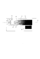
- FIG. 18 schematically shows a temperature distribution generated in the modulator housing 1704 when the optical modulator 1700 is mounted on a circuit board 1802 of an optical module together with, for example, a DSP 1800 which is a heat-generating electronic component.
- Black and white shading superimposed on the illustrated modulator housing 1704 indicates the temperature of each part, and the whiter the temperature, the lower the temperature, and the darker the temperature, the higher the temperature.
- heat from the DSP 1800 arranged on the lower right of the circuit board 1802 mainly propagates through the circuit board 1802, and the heat from the portion of the lower side of the modulator housing 1704 facing the DSP 1800 starts from the portion facing the DSP 1800. It flows into the housing 1704. Then, the heat that has flowed in from this portion propagates toward the entire modulator housing 1704 to the upper left in the figure.
- a temperature gradient is generated in the modulator housing 1704 such that the temperature decreases from the lower right to the upper left as shown in the figure.
- a temperature gradient does not occur when the entire temperature of the modulator housing 1704 changes with a change in the environmental temperature, and the DSP 1800 is unevenly distributed at an asymmetric position with respect to the modulator housing 1704. Occurs due to acting as a heat source. More specifically, this temperature gradient is due to the fact that the size of the DSP 1800 is generally smaller than the size of the modulator housing 1704, and that the DSP 1800 is located close to some of the sides of the modulator housing 1704. I do.
- the DSP 1800 acts as an asymmetrical unevenly distributed heat source as described above.
- the temperature gradient is equal to the center line 1720 with respect to the width direction of the modulator housing 1704 and the center line 1722 with respect to the longitudinal direction. It occurs along different directions 1804 (white dashed arrows in the figure), causing an asymmetric temperature distribution in the modulator housing 1704.
- Such an asymmetric temperature distribution in the modulator housing 1704 is caused by a temperature change expected by the conventional design idea of the modulator housing 1704 of “suppressing deformation by making the wall thickness of the four sides the same”, that is, This is significantly different from “uniform temperature change” in the modulator housing 1704, and may cause characteristic fluctuations and long-term reliability that exceed the designer's prediction.
- This temperature gradient causes the DSP 1800 to act as an asymmetric unevenly distributed heat source as described above, and as a result, the center line 1720 with respect to the width direction of the modulator housing 1704 and the center line 1722 with respect to the longitudinal direction as shown in FIG. This occurs along a direction 1804 (white dashed arrow in the drawing) that is different from the direction, and generates an asymmetric temperature distribution in the modulator housing 1704.
- Such an asymmetrical temperature distribution in the modulator housing 1704 causes a situation in which the design concept of the conventional modulator housing 1704, which is "suppressing deformation by making the wall thicknesses of the four sides the same", that is, the modulation This is significantly different from “uniform temperature change" in the housing 1704, and may cause characteristic fluctuations and long-term reliability lower than expected by the designer.
- a constant temperature chamber set at various temperatures for example, 100 ° C., 125 ° C., etc.
- An optical modulator to be tested is placed in each of the optical modulators, and the characteristic variation of each optical modulator is measured each time a predetermined elapsed time comes. That is, what is predicted from such an accelerated deterioration test is the long-term reliability when the optical modulator 1700 is continuously used at a uniform temperature. Therefore, the long-term reliability of the optical modulator 1700 in a situation where an asymmetric temperature distribution occurs in the optical module as described above may be significantly different from the above prediction.
- an asymmetric temperature distribution also occurs in the plane of the substrate constituting the light modulation element 1702. Accordingly, in particular, when the interferometric light modulator such as the Mach-Zehnder light modulator is used as the light modulator 1702 as described above, an asymmetric temperature distribution is formed between adjacent parallel waveguides on the substrate. Due to this, an additional phase difference different from each other occurs, which may have an unfavorable effect on the characteristics and reliability of the light modulation element 1702 itself.
- the asymmetric temperature distribution generated over a long period of time due to the close arrangement with the heat-generating electronic components causes the characteristic fluctuation and reliability that could not be foreseen in an accelerated deterioration test or the like. It is expected that the decline will occur particularly significantly.
- the heat flowing into the modulator housing from the heat-generating electronic components is reduced by the optical modulation elements and lenses such as lenses disposed in the modulator housing. It can easily propagate to the mounting position of the component, cause a characteristic change as an optical modulator, and reduce long-term reliability.
- One embodiment of the present invention includes a light modulation element including an optical waveguide formed over a substrate and a housing that houses the light modulation element, and the housing has a quadrilateral shape in plan view.
- the light modulating element is fixed to one short side wall, and the light modulating element is disposed such that a first end in a longitudinal direction of the light modulating element faces the first short side wall, and the housing is provided with the first light modulating element.
- At least a part of the light input / output unit which is a range from the outer surface of the one short side wall to the first end of the light modulation element, has a higher thermal resistance than a part of the housing other than the light input / output unit. It has a high heat resistance part.
- an average thickness of the first short side wall is smaller than an average thickness of each of the first long side wall and the second long side wall other than the light input / output section.
- the first short side wall is formed and constitutes the high thermal resistance portion.
- the first long side wall has an average of a portion of the first long side wall other than the light input / output portion, at least in a part of the portion included in the light input / output portion.
- the thin wall portion constitutes the high heat resistance portion.
- the bottom wall is formed to be thinner than an average thickness of the bottom wall in a part other than the light input / output unit, at least in a part included in the light input / output unit. It has a third thin wall portion, and the third thin wall portion of the bottom wall forms the high thermal resistance portion.
- an optical component is disposed on the third thin wall portion of the bottom wall.
- at least one of the optical components disposed on the third thin wall portion of the bottom wall is connected to the third thin wall portion of the bottom wall via a separate pedestal. Fixed to.
- the housing has a rear portion which is a range from a second end facing the first end of the light modulation element to an inner surface of the second short side wall,
- a drive circuit for driving the light modulation element is provided, and the bottom wall is formed such that an average thickness at the rear portion is larger than an average thickness at the light input / output portion, or
- the long side wall or the second long side wall is formed such that an average thickness at the back portion is larger than an average thickness at the light input / output portion.
- an optical component is fixed to the first end of the light modulation element, and the bottom wall has an inner surface having a height different from an outer surface of the bottom wall.
- a step portion connecting the two planes, and the light modulation element is arranged on the bottom wall such that the first end protrudes from the step portion.
- Another embodiment of the present invention is an optical module including any one of the above-described optical modulators and an electronic component. This specification includes all contents of Japanese Patent Application No. 2018-124467 filed on June 29, 2018.
- the optical modulator even when a heat source such as an electronic component is disposed close to the optical modulator, it is possible to suppress a change in characteristics and / or a decrease in long-term reliability.
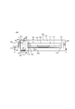
- FIG. 1 is a plan view of the optical modulator according to the first embodiment of the present invention.
- FIG. 2 is an AA cross-sectional view of the optical modulator shown in FIG.
- FIG. 3 is a diagram illustrating an example of a temperature distribution generated in a modulator housing when the optical modulator illustrated in FIG. 1 is mounted on a circuit board.
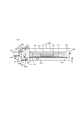
- FIG. 4 is a plan view of an optical modulator according to the second embodiment of the present invention.
- FIG. 5 is a sectional view of the optical modulator shown in FIG.
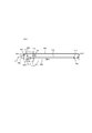
- FIG. 6 is a plan view of an optical modulator according to the third embodiment of the present invention.
- FIG. 7 is a cross-sectional view of the optical modulator shown in FIG.
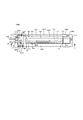
- FIG. 8 is a plan view of an optical modulator according to the fourth embodiment of the present invention.
- FIG. 9 is a sectional view of the optical modulator shown in FIG.
- FIG. 10 is a plan view of an optical modulator according to a fifth embodiment of the present invention.
- FIG. 11 is an EE sectional view of the optical modulator shown in FIG.
- FIG. 12 is a plan view of an optical modulator according to the sixth embodiment of the present invention.
- FIG. 13 is an FF cross-sectional view of the optical modulator shown in FIG.
- FIG. 14 is a plan view of the optical modulator according to the seventh embodiment of the present invention.
- FIG. 15 is a GG sectional view of the optical modulator shown in FIG.
- FIG. 16 is a plan view of an optical module according to the eighth embodiment of the present invention.
- FIG. 17 is a plan view showing a configuration of a conventional optical modulator.
- FIG. 18 is a diagram illustrating an example of a temperature distribution generated in a modulator housing when a conventional optical modulator is mounted on a circuit board.
- the present invention configures an optical modulator in which the proximity arrangement with a heat-generating electronic component is avoided in the related art as an optical device capable of the close arrangement, and also actively improves a thermal environment in the optical module. It opens the way for use as a device that can contribute.
- the thickness of the side wall of the modulator housing is adjusted so that the modulator housing itself actively acts as a heat sink or a good heat conductor.
- a housing configuration in which heat is easily transmitted to the entire light modulation element is adopted.
- the optical input / output unit on which the optical components are mounted is configured to be hard to conduct heat. This avoids asymmetrical temperature distribution in the light modulation element, avoids heat conduction to the optical components, and avoids fluctuations in characteristics and long-term reliability of the light modulator as a whole.
- the optical modulator of the present invention faces the one wall from the outer surface of the one wall on which the input optical fiber and the output optical fiber are arranged, of the modulator housing constituting the optical modulator. At least a part of the input / output section extending to one end of the light modulation element is provided with a high thermal resistance section having a higher thermal resistance than a part of the modulator housing other than the optical input / output section.
- the optical modulator according to the present embodiment has an average thickness of one wall of the modulator housing in which the input optical fiber and the output optical fiber are arranged, and the average thickness of each of the two walls connected to both sides of the one wall. , Which are formed thinner than the average thickness of portions other than the input / output portion to constitute a high thermal resistance portion.
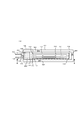
- FIG. 1 is a plan view showing the configuration of the optical modulator 100 according to the first embodiment of the present invention
- FIG. 2 is a cross-sectional view of the optical modulator 100 taken along the line AA.
- the light modulator 100 includes a light modulation element 102, a modulator housing 104 that houses the light modulation element 102, an input optical fiber 108 that inputs light to the light modulation element 102, and light output from the light modulation element 102. And an output optical fiber 110 for guiding the light to the outside of the modulator housing 104.
- the modulator housing 104 Since the modulator housing 104 is airtightly sealed, the inside of the modulator housing 104 cannot actually be visually recognized. However, in FIG. 1, the configuration inside the modulator housing 104 is understood. For simplicity, the components inside the modulator housing 104 are shown by solid lines.
- the modulator housing 104 is made of metal (for example, stainless steel, Kovar, or the like), and is rectangular or quadrilateral (for example, rectangular or substantially rectangular) in plan view. That is, the modulator housing 104 includes a first short side wall 120 and a second short side wall connected to the bottom wall 128 having a quadrilateral shape in a plan view and the other two opposite sides (left and right sides in the drawing) of the bottom wall 128. And a side wall 122. Further, the modulator housing 104 is provided on two opposing sides (upper and lower sides in FIG. 1) of the bottom wall 128 that are longer than the first short side wall 120 and the second short side wall 122. A first long side wall 124 and a second long side wall 126 are connected. The light modulation element 102 is housed in a space surrounded by the first short side wall 120, the second short side wall 122, the first long side wall 124, the second long side wall 126, and the bottom wall 128. .
- the end facing the first short side wall 120 where the light input terminal 150 and the light output terminal 152, which will be described later, are arranged is referred to as a first end 140, a first end 140. Is defined as a second end 142. Therefore, the second end 142 faces the second short side wall 122.
- a line extending in the left-right direction in the figure along the center of the modulator housing 104 in the width direction is a center line 130 with respect to the width direction
- a line extending in the vertical direction in the figure along the center in the longitudinal direction is defined as a center line 132 with respect to the longitudinal direction.
- the light modulation element 102 is a waveguide type light modulator composed of an optical waveguide formed on a substrate.
- the light modulation element 102 is configured by, for example, an optical waveguide provided on a LiNbO 3 substrate.
- the light modulation element 102 includes an input waveguide 112 into which light from the input optical fiber 108 is incident, a modulation unit 114 including an optical waveguide group that performs an optical modulation operation, and a light provided at the second end 142. It has a light reflection film 116 that constitutes a folded portion.
- the modulation unit 114 performs a modulation operation by causing light propagating in a plurality of optical waveguides extending in the longitudinal direction of the light modulation element 102 to interfere with each other, for example.
- the modulation unit 114 includes four Mach-Zehnder optical waveguides and four RF (Radio Frequency) electrodes (not shown) provided on the Mach-Zehnder optical waveguide and modulating a light wave propagating in the optical waveguide.
- a DP-QPSK optical modulator comprising:
- the first end 140 of the optical modulation element 102 is an optical input / output end to which the light from the input optical fiber 108 is input to the input waveguide 112 and the light modulated by the modulator 114 is output.
- the second end 142 on the right side in the drawing is a light turning end where light is turned back by the light reflecting film 116.
- a microlens array 118 as an optical component is fixed to the first end 140 by, for example, bonding.
- a glass block 144 for reinforcing the adhesive strength of the optical component is fixed to the substrate surface near the first end 140 by, for example, bonding.
- An optical input terminal 150 for holding the input optical fiber 108 and an optical output terminal 152 for holding the output optical fiber 110 are fixed to the first short side wall 120 of the modulator housing 104.
- a lens 154 which is an optical component for collimating the light from the input optical fiber 108, is disposed inside the light input terminal 150.
- a lens 158 and an optical polarization combining unit 156 which are optical components, are arranged.
- the polarization combining unit 156 is composed of a wave plate and a polarization combining prism, and outputs two lights (in the case of a DP-QPSK modulator, orthogonal X-axis ports and Y-axis ports) output from the modulation unit 114 of the light modulation element 102. (Port polarization) is polarization-combined and output as one light.
- the lens 158 collects the light output from the polarization combining unit 156 and inputs the collected light to the output optical fiber 110.
- the light input from the input optical fiber 108 is collimated by the lens 154 in the optical input terminal unit 150, and then is collimated by the microlens array 118 provided at the first end 140 of the light modulation element 102.
- the light is condensed and input to the input waveguide 112 of the light modulation element 102.
- the light input to the input waveguide 112 is reflected by the light reflecting film 116 at the second end 142, and is input to the modulator 114.
- the light input to the modulator 114 is modulated by the modulator 114 and then output from the first end 140.
- the light from the modulating unit 114 output from the first end 140 is collimated by the microlens array 118 and is polarized by the polarization combining unit 156 in the optical output terminal unit 152.
- the polarized light is condensed by the lens 158 in the optical output terminal unit 152, coupled to the output optical fiber 110, and guided to the outside of the modulator housing 104 by the output optical fiber 110.
- FIG. 2 also shows a cover 160 that constitutes a part of the modulator housing 104 in the opening at the upper part of the modulator housing 104 in the drawing.
- the cover 160 is provided with a first short side wall 120, a second short side wall 122, and a first long side wall in FIG. For example, seams are welded to four sides of the second long side wall 126.
- a plurality of lead pins for inputting a high-frequency signal for operating the light modulation element 102, and a high-frequency signal input from the plurality of lead pins are applied to the RF electrode of the light modulation element 102.
- a relay board or the like for guiding each of them may be provided (neither is shown). Therefore, irregularities are formed on the inner surfaces of the first short side wall 120, the second short side wall 122, the first long side wall 124, the second long side wall 126, and / or the bottom wall 128 of the modulator housing 104. Can be provided.
- the first short side wall 120 and the second short side of the modulator housing 104 are shown in FIGS.
- the wall 122, the first long side wall 124, the second long side wall 126, and the bottom wall 128 are described as having a uniform thickness.
- FIGS. 4 to 15 should be understood to be the same.
- the wall thickness t1 of the first short side wall 120 on the left side of the modulator housing 104 is the first long side wall 124 and the second long side wall 124.
- 126 is thinner (that is, a smaller value) than the wall thicknesses t2 and t3 of the portion other than the light input / output unit 162, which is a range from the outer surface of the first short side wall 120 to the first end 140 of the light modulation element 102. ) Is formed. That is, t1 ⁇ t2 and t1 ⁇ t3.
- the optical modulator 100 when the optical modulator 100 is mounted on a circuit board in the optical module, one of the first long side wall 124 and the second long side wall 126 having the wall thicknesses t2 and t3 is provided by the circuit.
- the heat-generating electronic components mounted on the substrate are arranged so as to face the side on which, for example, a DSP is mounted.
- FIGS. 1 and 2 do not show irregularities for disposing lead pins, relay boards, and the like, which may be provided in the actual modulator housing 104. . Therefore, the wall thickness of the first short side wall 120, the second short side wall 122, the first long side wall 124, the second long side wall 126, and the bottom wall 128 shown in FIGS. In some cases, it should be understood to indicate the average wall thickness at each wall. That is, in the present embodiment, the wall thickness t1 is an average value of the wall thickness of the first short side wall 120.
- the wall thicknesses t2 and t3 are the average values of the wall thicknesses of the first long side wall 124 and the second long side wall 126 other than the light input / output unit 162, respectively.
- wall thickness in this specification refers to the average value (average wall thickness) of the wall thickness of the corresponding wall or a part of the wall, unless otherwise specified.
- the “average value” of the wall thickness refers to an average value of a corresponding wall or a partial thickness of the wall, and is a case where the wall or the wall portion is connected to or intersects with an adjacent wall. This also refers to the average value of the thickness of the so-called “wall” itself or the portion of the "wall” itself, not including the connection or intersection.
- the curved portion Means the average value of the thickness of the "wall” itself or the "wall” itself.
- the wall thickness t2 of the first long side wall 124 and the wall thickness t3 of the second long side wall 126 in portions other than the light input / output unit 162 have a lower thermal resistance than the long side wall in the conventional optical modulator.
- the wall thickness t1 of the first short side wall 120 is set in a range of, for example, 0.5 mm or more and 1.0 mm or less.
- the modulator casing 104 can be used as a heat sink for heat-generating electronic components arranged in close proximity by using the modulator casing 104 as a propagation path for heat flowing from the outside.
- the first long side wall 124 and the third long side wall are configured to have irregularities
- the first long side wall 124 and the third long side wall are each formed to have a thickness of 1.7 mm to 4 mm.
- the wall thicknesses t2 and t3, which are the respective average wall thicknesses may be set in a range of 2.0 mm or more and 3.0 mm or less.
- the first short side wall 120 has a configuration having irregularities
- the first short side wall 120 is formed in a range of 0.3 mm to 1 mm in thickness
- the wall thickness t1 which is the average wall thickness, is reduced.
- the value may be set in a range of 0.5 mm or more and 1.0 mm or less.
- the wall thickness t2 of the first long side wall 124 and the wall thickness t3 of the second long side wall 126 are set to be thicker than the conventional optical modulator.
- the thermal resistance of the first long side wall 124 and the second long side wall 126 along the long side of the 104 is reduced, and the temperature gradient in the longitudinal direction of the modulator housing 104 is reduced by a conventional optical modulator (for example, FIG. 17 (light modulator 1700). If the temperature gradient in the longitudinal direction of the modulator housing 104 is reduced in this way, the direction of the temperature gradient when viewed as a whole of the modulator housing 104 is longer than the direction 1804 shown in FIG. It is a direction close to the direction. As a result, it is possible to suppress an asymmetric temperature distribution of the entire optical modulator 100 including the optical modulation element 102, and to suppress a characteristic variation and a decrease in long-term reliability.
- the optical modulator 100 can be used as a device that can positively contribute to the improvement of the thermal environment in the optical module by using the optical modulator 100 as a heat sink and / or a good thermal conductor of the heat-generating electronic component.
- the above-described effect of suppressing the asymmetric temperature gradient is obtained by setting the wall thickness t2 of the first long-side wall 124 and the wall thickness t3 of the third long-side wall to 2.5 with respect to the conventional average wall thickness of 1.5 mm as described above. It is particularly remarkable when the thickness is in the range of 0 mm or more and 3.0 mm or less, and the wall thickness t1 of the first short side wall 120 is in the range of 0.5 mm or more and 1.0 mm or less. The function as a heat sink is further enhanced.
- the wall thickness t1 of the first short side wall 120 included in the light input / output unit 162 is different from that of the first long side wall 124 and the second long side wall 126 other than the light input / output unit 162.
- the first short side wall 120 itself is formed to be thinner than the wall thicknesses t2 and t3 of the portion, and forms the high thermal resistance portion.
- the optical modulator 100 even when the heat-generating electronic components are arranged close to each other, the optical components such as the input optical fiber 108 and the lens 154 disposed inside the optical input terminal 150 and the optical output terminal 152 are provided.
- the wall thickness t2 of the first long side wall 124 and the wall thickness t3 of the second long side wall 126 are set to be thicker than those of the conventional optical modulator, so that heat-generating electronic components and the like can be used.
- the generated temperature gradient of the modulator housing 104 can be reduced, and the characteristic fluctuation and the long-term reliability can be further suppressed.
- FIG. 3 schematically shows a temperature distribution generated in the modulator housing 104 when the optical modulator 100 is mounted on a circuit board 392 of an optical module together with, for example, a DSP 390 as a heat-generating electronic component.
- Black and white shading superimposed on the modulator casing 104 shown in the figure indicates the temperature of each part, and the whiter the temperature, the lower the temperature, and the darker the temperature, the higher the temperature.
- the temperature gradient along the center line 130 with respect to the width direction becomes gentle.
- the symmetry of the temperature distribution generated in the modulator housing 104 is improved.
- the stress generated in the modulator housing 104 is reduced and dispersed.
- the temperature distribution of the optical modulation device 102 which is an interferometric light modulation device, housed in the modulator housing 104 also has more symmetry. It becomes. As a result, the difference in the optical path length or the phase change between the parallel waveguides forming the light modulation element 102 is reduced, and the characteristic fluctuation (for example, the operation point fluctuation) of the light modulation element 102 is also suppressed.
- the modulator casing 104 in the optical module is placed in a uniform temperature environment as in a long-term reliability test in a thermostat. Approaching the state. Therefore, the long-term reliability of the modulator casing 104 approaches the long-term reliability test result of the thermostat, and can be further improved as compared with the conventional configuration.
- the wall thickness t4 of the second short side wall 122 shown in FIG. 1 and the wall thickness t5 of the portion other than the light input / output unit 162 in the bottom wall 128 shown in FIG. From the viewpoints of heat dissipation, rigidity, and the like, the larger the better, the better. For example, it is desirable that t4> t2 and t4> t3, and t5> t2 and t5> t3, respectively.
- the wall thickness t1 of the first short side wall 120 is made smaller than the wall thickness t2 of the first long side wall 124 and the wall thickness t3 of the second long side wall 126, so that the high thermal resistance portion is formed.
- the material of the first short side wall 120 is changed to the first long side wall 124,
- the second long side wall 126 and / or the bottom wall 128 (more specifically, a material other than the light input / output portion 162 of these walls) is made of another material having a lower thermal conductivity.
- the first short side wall 120 may be configured as a high heat resistance portion.
- the optical modulator according to the present embodiment has an input / output unit which is a range from the outer surface of the first short side wall on which the input optical fiber and the output optical fiber are arranged to the first end of the optical modulation element.
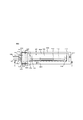
- FIG. 4 is a plan view showing the configuration of the optical modulator 400 according to the second embodiment.
- FIG. 5 is a sectional view of the optical modulator 400 shown in FIG. 4 and 5, the same reference numerals as those in FIGS. 1 and 2 denote the same components and wall thicknesses as those of the optical modulator 100 according to the first embodiment in FIGS. 1 and 2, respectively. It shall be used, and the description of the optical modulator 100 described above shall be cited. Further, in FIG. 4, in order to facilitate understanding of the configuration of the optical modulator 400, similarly to FIG. 1, the internal structure that cannot be visually recognized after the assembly is completed is shown by a solid line.
- the optical modulator 400 has a configuration similar to that of the optical modulator 100, except that a modulator housing 404 is provided instead of the modulator housing 104.
- the modulator housing 404 includes a first short side wall 420 similar to the first short side wall 120, the second short side wall 122, the first long side wall 124, and the second long side wall 126 of the modulator housing 104. , A second short side wall 422, a first long side wall 424, and a second long side wall 426. That is, the first length of the portion other than the light input / output unit 462 where the wall thickness t1 of the first short side wall 420 is in the range from the outer surface of the first short side wall 420 to the first end 140 of the light modulation element 102.
- the wall thickness t2 of the side wall 424 and the wall thickness t3 of the second long side wall 426 are configured such that t1 ⁇ t2 and t1 ⁇ t3.
- the modulator housing 404 is different from the modulator housing 104 in having a bottom wall 428 instead of the bottom wall 128.
- the bottom wall 428 has a thin wall portion having at least a part of the light input / output unit 462 having a wall thickness t52 smaller than the wall thickness t51 of the bottom wall 428 in a part other than the light input / output unit 462. 464 (illustrated dot hatching portion).
- the thin wall portion 464 corresponds to a third thin wall portion.
- FIG. 5 also illustrates a cover 460 that forms a part of the housing 406.
- the modulator housing 404 shown in FIG. 4 has, like the modulator housing 104 shown in FIG. 1, unevenness for arranging lead pins, relay boards, and the like which may be provided in the actual modulator housing 404. Not shown. That is, the wall thickness of the first short side wall 420, the second short side wall 422, the first long side wall 424, the second long side wall 426, and the bottom wall 428 shown in FIG. Should be understood to indicate the average wall thickness at When the thin wall portion 464 is formed of, for example, a plurality of irregularities having different depths and opening sizes, the range of the thin wall portion 464 can be defined as a region including the irregularities.
- the optical modulator 400 having the above configuration, similarly to the optical modulator 100, heat flows along the first long side wall 424 and the second long side wall 426 which are thicker than the wall thickness of the conventional optical modulator.
- the temperature gradient becomes gentle on both the first long side wall 424 side and the second long side wall 426 side, and the symmetry of the temperature distribution generated in the modulator housing 404 is improved. Thereby, even when the optical modulator 400 is arranged close to the heat-generating electronic component, the fluctuation of the characteristics of the optical modulator 400 and the decrease in long-term reliability are suppressed.
- the first short side wall 420 has the first long side wall 424 and the second long side wall 424 other than the light input / output unit 462.
- the side wall 426 is formed with a wall thickness t1 smaller than the wall thicknesses t2 and t3, and forms a high thermal resistance portion.
- a thin wall portion 464 having a wall thickness t52 smaller than the wall thickness t51 of the portion other than the light input / output portion 462 is formed also on the bottom wall 428 to constitute a high thermal resistance portion.
- the heat flowing into the light input terminal 150 and the light output terminal 152 from the bottom wall 428 through the first short side wall 420 by the thin wall portion 464 is also suppressed, and the light modulation is performed.
- the optical modulator 100 it is possible to suppress the occurrence of the characteristic fluctuation and the decrease in the long-term reliability of the optical modulator 400.
- a thin wall portion 464 is provided on the bottom wall 428 to form a high heat resistance portion.
- the high heat resistance portion may be constituted only by the thin wall portion 464 of the bottom wall 428, and the first short side wall 420 may be constituted by a wall thickness equivalent to t2 and t3.
- the material of the first short side wall 420 is used to configure a portion other than the light input / output unit 462.
- the first short side wall 420 is configured as a high thermal resistance portion by using a material having a lower thermal conductivity than the material of the first long side wall 424, the second long side wall 426, and / or the bottom wall 428. It may be.
- the material of the portion of the bottom wall 428 corresponding to the thin wall portion 464 is replaced with the first long side wall constituting the portion other than the light input / output portion 462.
- the material corresponding to the thin wall portion 464 may be configured as a high thermal resistance portion by using a material having a lower thermal conductivity than that of the portion of the 424, the second long side wall 426, and / or the bottom wall 428. .
- the optical modulator according to this embodiment includes an outer surface of the first short side wall of each of the first long side wall and the second long side wall connected to the first short side wall on which the input optical fiber and the output optical fiber are arranged. And at least a part of the light input / output unit in the range from the light input / output unit to the first end of the light modulation element. It has a first thin wall portion and a second thin wall portion having a smaller average wall thickness. The first thin wall portion and the second thin wall portion constitute a high heat resistance portion as a characteristic configuration.
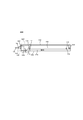
- FIG. 6 is a plan view showing the configuration of the optical modulator 600 according to the third embodiment.
- FIG. 7 is a cross-sectional view of the optical modulator 600 shown in FIG. 6 and 7, the same reference numerals as those in FIGS. 1 and 2 are used for the same components as those in the optical modulator 100 according to the first embodiment in FIGS. 1 and 2, respectively.
- the description of the optical modulator 100 described above is referred to.
- FIG. 6 in order to facilitate understanding of the configuration of the optical modulator 600, the internal structure that cannot be visually recognized after the assembly is completed is indicated by solid lines, as in FIG.
- FIG. 7 also shows a cover 660 that forms a part of the modulator housing 604, which is not shown in FIG.
- the optical modulator 600 has the same configuration as that of the optical modulator 100, except that the optical modulator 600 includes a modulator housing 604 instead of the modulator housing 104.
- the modulator housing 604 is similar to the first short side wall 120, the second short side wall 122, the first long side wall 124, the second long side wall 126, and the bottom wall 128 of the modulator housing 104, respectively. It has a first short side wall 620, a second short side wall 622, a first long side wall 624, a second long side wall 626, and a bottom wall 628.
- the first short side wall 620 has a range of light from the outer surface of the first short side wall 620 of the first long side wall 624 and the second long side wall 626 to the first end 140 of the light modulation element 102.
- Portions other than the input / output unit 662 are configured to have a wall thickness t11 smaller than the wall thicknesses t21 and t31 to form a high thermal resistance unit.
- the bottom wall 628 has a thin wall portion 664 (dots shown in the drawing) having a wall thickness t54 smaller than a wall thickness t53 of a portion of the bottom wall 628 other than the light input / output portion 662 at least at a part of the light input / output portion 662. (A hatched portion) is formed.
- first long side wall 624 has at least a part of the light input / output unit 662 with a wall thickness t22 that is smaller than the wall thickness t21 of the portion other than the light input / output unit 662 in the first long side wall 624.
- a thin wall portion 670 (hatched right oblique portion in the figure) is formed.
- the second long side wall 626 has at least a part of the light input / output unit 662 with a wall thickness t32 that is smaller than the wall thickness t31 of the portion other than the light input / output unit 662 in the second long side wall 626.
- a thin wall portion 672 (a left oblique hatching portion in the figure) is formed.
- the thin wall portions 670, 672, and 664 correspond to the first thin wall portion, the second thin wall portion, and the third thin wall portion, respectively.
- the optical modulator 600 having the above configuration, as in the optical modulator 100, heat flows along the first long side wall 624 and the second long side wall 626, which are thicker than the wall thickness of the conventional optical modulator.
- the temperature gradient is gentle on both the first long side wall 624 side and the second long side wall 626 side, and the symmetry of the temperature distribution generated in the modulator housing 604 is improved.
- the optical modulator 600 since the first short side wall 620 and the thin wall portions 664, 670, and 672 constitute a high thermal resistance portion, when the optical modulator 600 is mounted on an optical module or the like, modulation is performed from a DSP or the like which is a heat-generating electronic component. Heat flowing into the housing 604 can be effectively suppressed from flowing into the light input terminal 150 and the light output terminal 152. Thus, the optical modulator 600 can further suppress the occurrence of characteristic fluctuations and / or a decrease in long-term reliability of the optical modulator 600 as compared with the optical modulator 100.
- the first long side wall 624 and the second long side wall 626 are configured such that the wall thicknesses t21 and t31 satisfy t21 ⁇ t31.
- Such a configuration is convenient when, for example, when the optical modulator 600 is mounted on the optical module, it can be defined that the heat-generating electronic component is mounted on one of the long side walls.
- the wall thickness of the long side wall for example, the second long side wall 626 in the present embodiment
- these two long side walls are formed. In this case, the heat from the heat-generating electronic components can be more effectively transmitted to the circuit board with the same weight as compared with the configuration in which the wall thicknesses are the same.
- the thin wall portions 664, 670, 672 are provided, but the present invention is not limited to this. Even if only the thin wall portions 670 and 672 are provided without providing the thin wall portion 664, a certain suppression effect can be obtained with respect to the above-mentioned characteristic fluctuation and reliability reduction.
- the optical modulator according to the present embodiment has the same configuration as the optical modulator 600 according to the third embodiment, and an optical component is disposed on the thin wall portion 664 of the bottom wall 628.
- FIG. 8 is a plan view showing the configuration of the optical modulator 800 according to the fourth embodiment
- FIG. 9 is a cross-sectional view of the optical modulator 800 shown in FIG. 8 and 9, the same components as those of the optical modulator 600 according to the third embodiment in FIGS. 6 and 7 and the optical modulator 100 according to the first embodiment in FIGS.
- the same reference numerals as those in FIGS. 6 and 7 and FIGS. 1 and 2 are used, and the description of the optical modulators 400 and 100 described above is used.
- FIG. 8 in order to facilitate understanding of the configuration of the optical modulator 800, similarly to FIGS. 1 and 4, the internal structure that cannot be visually recognized when assembly is completed is indicated by solid lines. I have.
- the optical modulator 800 has the same configuration as the optical modulator 600, but includes an optical output terminal 852 instead of the optical output terminal 152, and includes a high thermal resistance portion of the bottom wall 628 of the modulator housing 604. The difference is that an optical component group 876 is arranged on the thin wall portion 664 to be configured.
- the optical output terminal unit 852 has the same configuration as the optical output terminal unit 152, but differs from the optical output terminal unit 152 in that the optical output terminal unit 852 does not include the polarization combining unit 156.
- the optical component group 876 includes, for example, optical components having the same function as the optical components such as the polarization combining unit 156 disposed in the optical output terminal unit 152 of the optical modulator 600, and includes, for example, a wave plate and a polarization combining unit. Prism included.
- arranging optical components in an optical output terminal unit is advantageous for downsizing an optical modulator, but restricts the size, shape, and / or characteristics of the optical components, and limits the choice of optical components. Will be done. Further, as compared with a configuration in which the optical components are disposed in the modulator housing, the distance from the light output end face of the light modulation element to the optical components is longer, so that the light emitted from the light modulation element due to temperature fluctuation or the like is emitted. Even if the angle fluctuates slightly, the point of incidence of light on the optical component fluctuates greatly, and the temperature characteristics of the optical characteristics tend to deteriorate.
- the optical component group 876 is disposed on the thin wall portion 664 of the bottom wall 628 of the modulator housing 604, for example, a polarization combining prism, a wavelength plate, or the like constituting the optical component group 876.
- the restrictions on the shape (size) and characteristics (for example, dependence on the light incident point) are relaxed. For this reason, options of these optical components are expanded.
- the distance from the first end 140 of the light modulation element 102 to the optical component group 876 having, for example, a polarization combining prism or the like is smaller. It is possible to do. For this reason, a change in optical characteristics with respect to a change in the emission angle of light from the light modulation element 102 due to a temperature change can also be suppressed.
- the optical component group 876 may include one or a plurality of optional optical components according to the function required of the optical modulator 800 and the like.
- the output optical fiber 110 may be drawn into the interior of the modulator housing 604, and the lens 158 disposed in the light output terminal portion 852 may be included in the optical component group 876.
- the input optical fiber 108 may be drawn into the interior of the modulator housing 604, and the lens 154 provided in the optical input terminal 150 may be included in the optical component group 876.
- the optical modulator according to the present embodiment has the same configuration as the optical modulator 800 according to the fourth embodiment, and at least one of the optical components arranged on the thin wall portion 664 of the bottom wall 628 is different from the optical modulator 800 according to the fourth embodiment. It is characterized in that it is fixed to the thin wall portion 664 via a pedestal formed of a body.
- FIG. 10 is a plan view showing the configuration of the optical modulator 1000 according to the fifth embodiment
- FIG. 11 is a cross-sectional view of the optical modulator 1000 shown in FIG.
- the same components and wall thicknesses as those of the optical modulator 800 according to the fourth embodiment in FIGS. 8 and 9 are denoted by the same reference numerals as those in FIGS.
- the description of the optical modulator 800 described above is referred to.
- FIG. 10 in order to facilitate understanding of the configuration of the optical modulator 1000, similarly to FIG. 8, the internal structure that cannot be visually recognized after the assembly is completed is indicated by a solid line.
- the optical modulator 1000 has the same configuration as the optical modulator 600, but the optical component group 876 is attached to the thin wall portion 664 of the bottom wall 628 of the modulator housing 604, which constitutes a high thermal resistance portion, via the base 1078. Is different.
- a pedestal 1078 made of a material having low thermal conductivity (for example, ceramic or the like) is sandwiched between the thin wall portion 664 of the bottom wall 628 and the optical component group 876. And two thermal interfaces can be sandwiched (i.e., the interface between thin wall 664 and pedestal 1078 and the interface between pedestal 1078 and optics group 876). . For this reason, heat conduction from the thin wall portion 664 to the optical component can be largely suppressed.
- the optical modulator 1000 after mounting an optical component group 876 including a plurality of optical components on the pedestal 1078, the optical components 1000 are assembled on the pedestal 1078, and the pedestal 1078 and The group of optical components 876 can be disposed on the thin wall portion 664 of the bottom wall 628. For this reason, the handling of the optical component is facilitated, the number of manufacturing steps can be reduced, and the manufacturing variation can be reduced.
- all of the optical components arranged on the thin wall portion 664 constitute an optical component group 876 and are fixed on the thin wall portion 664 via the pedestal 1078.
- At least one of the optical components disposed on the thin wall portion 664 constitutes an optical component group 876 according to the heat resistance of the optical components, the ease of adjustment when manufacturing the optical modulator 1000, and the like. , May be fixed on the thin wall portion 664 via the pedestal 1078.
- the optical modulator according to the present embodiment has an optical modulator on a rear portion which is a range from a second end facing the first end of the optical modulator to an inner surface of the second short side wall of the modulator housing. Is provided as a characteristic configuration. Further, the bottom wall of the modulator housing has an average thickness at the back portion that is greater than an average thickness at the light input / output portion that is in a range from the outer surface of the first short side wall to the first end of the light modulation element. It is also characterized in that the first long side wall or the second long side wall is formed to be thicker, and the average thickness at the rear portion is larger than the average thickness at the light input / output portion. Is included.
- FIG. 12 is a plan view showing the configuration of an optical modulator 1200 according to the sixth embodiment
- FIG. 13 is a cross-sectional view of the optical modulator 1200 shown in FIG. 12 and 13, the same reference numerals as those in FIGS. 10 and 11 are used for the same components and wall thicknesses as those of the optical modulator 1000 according to the fifth embodiment in FIGS.
- the description of the optical modulator 1000 described above is referred to.
- FIG. 12 in order to facilitate understanding of the configuration of the optical modulator 1200, the internal structure that cannot be visually recognized in a state where the assembly is completed is shown by a solid line, similarly to FIG.
- the optical modulator 1200 has the same configuration as the optical modulator 1000, but differs in that a modulator housing 1204 is provided instead of the modulator housing 604.
- the modulator housing 1204 is similar to the first short side wall 620, the second short side wall 622, the first long side wall 624, the second long side wall 626, and the bottom wall 628 of the modulator housing 604. It has one short side wall 1220, a second short side wall 1222, a first long side wall 1224, a second long side wall 1226, and a bottom wall 1228.
- the first short side wall 1220 is a range of the first long side wall 1224 and the second long side wall 1226 from the outer surface of the first short side wall 1220 to the first end 140 of the light modulation element 102. It is formed so as to have a wall thickness t12 smaller than the wall thicknesses t25 and t35 of the portion other than the light input / output unit 1262, and constitutes a high thermal resistance unit.
- the bottom wall 1228 has a thin wall portion 1264 having a wall thickness t56 smaller than a wall thickness t55 of a portion other than the light input / output portion of the bottom wall 1228 on at least a part of the light input / output portion 1262. Is formed. Note that FIG. 13 also illustrates a cover 1260 that forms a part of the modulator housing 1204 whose description is omitted in FIG.
- the first long side wall 1224 further includes at least a part of the light input / output unit 1262, a wall thinner than the wall thickness t ⁇ b> 25 of a portion of the first long side wall 1224 other than the light input / output unit 1262.
- a thin wall portion 1270 having a thickness t26 is formed.
- the second long side wall 1226 has a thin wall thickness t36 at at least a part of the light input / output unit 1262 that is smaller than a wall thickness t35 of a portion of the second long side wall 1226 other than the light input / output unit 1262.
- a wall 1272 is formed.
- the thin wall portions 1270, 1272, and 1264 correspond to the first thin wall portion, the second thin wall portion, and the third thin wall portion, respectively, and constitute high heat resistance portions.
- an optical component group 876 is fixed via a pedestal 1078.
- a drive circuit for driving the light modulation element 102 is provided on a rear portion 1280 that extends from the second end 142 of the light modulation element 102 to the inner surface of the second short side wall 1222.
- a driver IC 1282 is provided.
- the bottom wall 1228 of the modulator housing 1204 has a wall thickness t57 of the rear portion 1280 that is equal to a wall thickness t58 of the optical input / output unit 1262 (that is, an average wall thickness of the optical input / output unit 1262). It is formed thicker than a certain wall thickness t58).
- the first long side wall 1224 and the second long side wall 1226 have wall thicknesses t27 and t37 of the rear portion 1280, respectively, and wall thicknesses t28 and t38 of the light input / output unit 1262 (that is, the light input / output unit 1262). It is formed to be thicker than the respective average wall thicknesses t28 and t38).
- the optical modulator 1200 having the above configuration, similarly to the optical modulator 100, heat flows along the first long side wall 1224 and the second long side wall 1226 which are thicker than the wall thickness of the conventional optical modulator.
- the temperature gradient becomes gentle on both the first long side wall 1224 side and the second long side wall 1226 side, and the symmetry of the temperature distribution generated in the modulator housing 1204 is improved.
- the optical modulator 1200 is arranged close to the heat-generating electronic components, the fluctuation of the characteristics of the optical modulator 1200 and the decrease in long-term reliability are suppressed.
- the optical modulator 1200 has a thin wall portion 1264 and the like constituting a high thermal resistance portion, similarly to the optical modulators 100, 400, 600, 800, and 1000 according to the first to fifth embodiments. Variations in characteristics and a decrease in long-term reliability when the heat-generating electronic components are arranged close to each other can be suppressed.
- the driver IC 1282 for driving the optical modulation element 102 is disposed adjacent to the optical modulation element 102, the transmission distance of the high-frequency signal from the driver IC 1282 to the optical modulation element 102 And the high-frequency characteristics of the entire light modulation operation can be greatly improved.
- the driver IC 1282 is generally a heat-generating electronic component that can generate heat of about 1 W.
- the driver IC 1282 is disposed close to the outside of the optical modulator in the optical module as in the related art, the driver IC 1282 is unevenly distributed with respect to the optical modulator. Acting as a heat source to generate an asymmetric temperature distribution in the housing of the optical modulator.
- the driver IC 1282 is disposed on the rear portion 1280 of the modulator housing 1204 facing the optical input / output portion 1262, and the wall thickness t57 of the bottom wall 1228 of the rear portion 1280 is provided.
- first long side wall 1224 and the second long side wall 1226 have wall thicknesses t27 and t37 of the rear portion 1280 on which the driver IC 1282 is disposed, respectively.
- the second long side wall 1226 is formed to be thicker than the wall thicknesses t28 and t38.
- the heat generated by the driver IC 1282 can flow substantially symmetrically in the width direction of the modulator housing 1204, and the temperature distribution of the modulator housing 1204 caused by the heat is substantially symmetric. Can be generated. That is, in the optical modulator 1200, the driver IC 1282 which acts as a heat source unevenly distributed in the related art is arranged at a position inside the modulator housing 1204 where no asymmetrical temperature distribution is generated. The heat environment of the driver IC 1282 can be secured while improving the thermal environment of the modulator 1200 itself.
- the wall thickness t57 of the rear wall 1280 of the bottom wall 1228 is formed to be thicker than the wall thickness t58 of the light input / output unit 1262, and the first long side wall 1224 and the second long side wall 1224 are formed.
- the wall thicknesses t27 and t37 of the rear portion 1280 are formed to be thicker than the wall thicknesses t28 and t38 of the light input / output unit 1262, respectively, but this is not a limitation.
- the modulator housing 1204 is That the bottom wall 1228 has a wall thickness t57 at the rear portion 1280 that is greater than the wall thickness t58 of the light input / output unit 1262;
- the first long side wall 1224 is formed such that the wall thickness t27 at the back portion 1280 is larger than the wall thickness t28 at the light input / output unit 1262; or If the second long side wall 1226 has one of the requirements that the wall thickness t37 of the rear portion 1280 is larger than the wall thickness t38 of the light input / output portion 1262, the same effect as described above is provided. Can be obtained at a certain level.
- an optical component is fixed to the first end of the light modulation element, and the bottom wall of the modulator housing has a different height on the inner surface from the outer surface of the bottom wall.
- the light modulating element includes two planes, and the light modulating element is arranged on the bottom wall such that the first end protrudes from a step formed by the two planes.
- FIG. 14 is a plan view showing the configuration of an optical modulator 1400 according to the seventh embodiment
- FIG. 15 is a sectional view of the optical modulator 1400 shown in FIG. 14 and 15, the same components and wall thicknesses as those of the optical modulator 1200 according to the sixth embodiment in FIGS. 12 and 13 use the same reference numerals as those in FIGS. 12 and 13.
- the above description of the optical modulator 1200 is referred to.
- FIG. 14 in order to facilitate understanding of the configuration of the optical modulator 1400, similarly to FIG. 12, an internal structure that cannot be visually recognized in a state where the assembly is completed is shown by a solid line.
- the micro lens array 118 as an optical component is fixed to the first end 140 of the optical modulation element 102 by, for example, bonding.
- the optical modulator 1400 has the same configuration as the optical modulator 1200, except that the optical modulator 1400 includes a modulator housing 1404 instead of the modulator housing 1204.
- the modulator housing 1404 is similar to the first short side wall 1220, the second short side wall 1222, the first long side wall 1224, the second long side wall 1226, and the bottom wall 1228 of the modulator housing 1204. It has a first short side wall 1420, a second short side wall 1422, a first long side wall 1424, a second long side wall 1426, and a bottom wall 1428.
- the first short side wall 1420 is a range from the outer surface of the first short side wall 1420 to the first end 140 of the light modulation element 102 among the first long side wall 1424 and the second long side wall 1426. It is formed so as to have a wall thickness t12 smaller than the wall thicknesses t25 and t35 of the portion other than the light input / output unit 1462, and constitutes a high thermal resistance unit.
- the bottom wall 1428 has a thin wall portion having at least a part of the light input / output unit 1462 having a wall thickness t56 smaller than a wall thickness t55 of a portion of the bottom wall 1428 other than the light input / output unit 1462. 1464 are formed. Note that FIG. 15 also illustrates a cover 1460 that constitutes a part of the modulator housing 1404, the description of which is omitted in FIG.
- the first long side wall 1424 has at least a part of the light input / output unit 1462 provided with a wall thinner than the wall thickness t25 of a portion of the first long side wall 1424 other than the light input / output unit 1462.
- a thin wall portion 1470 having a thickness t26 is formed.
- the second long side wall 1426 has a thin wall thickness t36 which is smaller than the wall thickness t35 of a portion of the second long side wall 1426 other than the light input / output unit 1462 in at least a part of the light input / output unit 1462.
- a wall 1472 is formed.
- the thin wall portions 1470, 1472, and 1464 correspond to the first thin wall portion, the second thin wall portion, and the third thin wall portion, respectively, and constitute high heat resistance portions.
- an optical component group 876 is fixed via a pedestal 1078.
- a drive circuit for driving the light modulation element 102 is provided on a rear portion 1480 of the modulator housing 1404, which is a range from the second end 142 of the light modulation element 102 to the inner surface of the second short side wall 1422.
- a driver IC 1282 is provided.
- the bottom wall 1428 of the modulator housing 1404 has a wall thickness t57 of the rear portion 1480 that is greater than a wall thickness t59 of the light input / output unit 1462 (that is, a wall thickness t59 that is an average wall thickness of the light input / output unit 1462). It is also formed thick. Further, the first long side wall 1424 and the second long side wall 1426 have wall thicknesses t27 and t37 of the rear portion 1480, respectively, and wall thicknesses t29 and t39 of the light input / output unit 1462 (that is, the light input / output unit 1462). It is formed to be thicker than the respective average wall thicknesses t29 and t39).
- the bottom wall 1428 of the modulator housing 1404 is formed on the inner surface thereof as two planes having different heights from the outer surface of the bottom wall 1428 on the upper surface of the thin wall portion 1464 in FIG. It has a certain thin-walled inner surface 1484 and a modulator fixing surface 1486 to which the light modulation element 102 is fixed.
- the thin wall inner surface 1484 and the modulator fixing surface 1486 constitute a step portion 1488.
- the light modulation element 102 modulates the bottom wall 1428 such that the first end 140 protrudes in the direction of the thin wall inner surface 1484 from the step 1488 formed by the thin wall inner surface 1484 and the modulator fixing surface 1486.
- the container fixing surface 1486 is provided.
- the optical modulator 1400 since the first end portion 140 of the optical modulation element 102 protrudes from the step portion 1488, the optical modulator 1400 is an optical component that is relatively sensitive to heat and temperature.
- the fixing portion between the lens array 118 and the first end 140 is separated from the bottom wall 1428. Thereby, heat conduction to the fixing portion is further suppressed. As a result, fluctuations in characteristics and a decrease in long-term reliability due to the close arrangement of the heat-generating electronic components are further suppressed.
- the micro lens array 118 is shown as an optical component fixed to the first end 140, but the present invention is not limited to this.
- An arbitrary optical component can be fixed to the first end 140 of the light modulation element 102.
- Such an optical component is, for example, one or more of a wave plate, a glass plate for a spacer, a lens, a prism, a PBC, a wave plate, a collimator, an anisotropic crystal, a sapphire plate, a glass plate, and a capillary. can do.
- the wall thicknesses t59, t29, and t39 which are the average wall thickness in the light input / output unit 1462, are different.
- the thin wall portions 1470 and 1472 may be provided on at least a part of the light input / output unit 1462.
- one of the two planes which the bottom wall 1428 of the modulator housing 1404 has on its inner surface is constituted by the thin wall inner surface 1484 which is the upper surface of the thin wall portion 1464.
- One of the two planes may be a plane formed in the light input / output unit 1462 other than the thin wall inner surface 1484, as long as it forms a step with at least the modulator fixing surface 1486. it can.
- the thin wall portion 1464 may be formed not in the entire area of the light input / output section 1462 but in at least a part thereof.
- This embodiment is an optical module including the optical modulator according to any of the above-described embodiments and an electronic component.
- FIG. 16 is a plan view showing a configuration of an optical module 1600 according to the eighth embodiment.
- the optical module 1600 houses the optical modulator 800 and the circuit board 1606 in the optical module housing 1602.
- an LD (Laser @ Diode) 1608 as a light source of transmission light and a PD (Photo @ Diode) 1610 as a light receiver of reception light are mounted on the circuit board 1606, in addition to the optical modulator 800.
- LD Laser @ Diode
- PD Photo @ Diode
- FIG. 16 shows a DSP 1612 for digital signal processing as an example of an electronic component that is a main electronic component and generates a large amount of heat.
- optical module 1600 can be mounted on the circuit board 1606 according to the functions required for the optical module 1600.
- electronic components include, for example, a driver IC for driving the optical modulator 100 and the like.
- the optical module 1600 outputs, for example, signal light (transmission light) to one transmission line optical fiber (not shown) via the optical modulator 800, and transmits the other transmission line optical fiber (not shown).
- the received optical signal (received light) is received by the PD 1610.
- the optical modulator 800 is arranged such that the DSP 1612 is arranged close to the second long side wall 626 having a greater wall thickness than the first long side wall 624 with a predetermined interval g.
- the interval g is, for example, 5 mm.
- the optical module 1600 having the above configuration uses the optical modulator 800 in which the characteristic fluctuation and the long-term reliability deterioration due to the close arrangement of the heat-generating electronic components are used, so that the optical modulator 800 is separated from the electronic components. It is possible to maintain a high transmission quality of the transmission light output from the optical module 1600 while suppressing downsizing of the optical module 1600 by relaxing the restriction on the distance, and to suppress a decrease in long-term reliability of the optical module 1600 as a whole. it can.
- the optical module 1600 is configured by using the optical modulator 800, but is not limited thereto.
- the optical modulator 100, 400, 600, 1000, 1200, or 1400 is arranged at the same position as the optical modulator 800 on the circuit board 1606 shown in FIG. You may comprise.
- the optical modulator 100 and the like include the optical modulator 102 including the optical waveguide formed on the substrate and the modulator housing 104 and the like that house the optical modulator.
- the modulator housing 104 and the like include a bottom wall 128 and the like having a quadrilateral shape in plan view, a first short side wall 120 and a second short side wall 122 and the like connected to two opposing sides of the bottom wall 128 and the like, The first long side wall 124 and the second long side wall which are longer than the first short side wall 120 and the like and the second short side wall 122 and the like and are connected to the other two opposite sides such as the bottom wall 128 etc. 126 and the like.
- the light modulation element 102 is located in a space surrounded by the bottom wall 128, the first long side wall 124, the second long side wall 126, and the like, and the first short side wall 120, the second short side wall 122, and the like. Is housed in Also, an optical input terminal unit 150 that holds an input optical fiber 108 for inputting light to the light modulation element 102 and an output optical fiber 110 that guides light output from the light modulation element 102 to the outside such as the modulator housing 104 are provided. The held light output terminal 152 and the like are both fixed to the first short side wall 120 and the like. Further, the light modulation element 102 is arranged such that the first end 140 in the longitudinal direction of the light modulation element 102 faces the first short side wall 120 or the like.
- the modulator housing 104 and the like are connected to at least a part of the optical input / output unit 162 or the like extending from the outer surface of the first short side wall 120 or the like to the first end 140 of the optical modulation element 102. It has a high thermal resistance portion having a higher thermal resistance than portions of the modulator housing 104 and the like other than the portion 162 and the like.
- the optical modulator 100 and the like are arranged close to the heat-generating electronic components such as the DSP 390 in the optical module as the optical communication device, the symmetry of the temperature distribution generated in the modulator housing 104 is achieved. And suppressing the propagation of heat to the first short side wall 120 or the like where the optical fiber or the optical component can be arranged, thereby suppressing the characteristic fluctuation and / or the long-term reliability decrease in the optical modulator 100 and the like. Can be.
- the wall thickness of the modulator housing 104 or the like other than the optical input / output section 162 or the like is increased while suppressing characteristic fluctuations and long-term reliability deterioration. Since the heat of the heat-generating electronic components can be transmitted, the optical modulator 100 and the like can be used as a heat sink and / or a good heat conductor that can positively contribute to the improvement of the thermal environment in the optical module.
- the wall thickness t11 of the first short side wall 120 is equal to the wall thicknesses t2 and t3 of the first long side wall 124 and the second long side wall 126 other than the light input / output unit 162.
- the first short side wall 120 is formed to be thinner and constitutes a high thermal resistance portion. According to this configuration, while improving the symmetry of the temperature distribution generated in the modulator housing 104 and further configuring the first short side wall 120 itself as a high thermal resistance portion, the input optical fiber 108 and the output optical fiber It is possible to suppress the flow of heat into the optical components such as the lens 110 and the lens 154, and to suppress the fluctuation of the characteristics of the optical modulator 100 and the decrease in long-term reliability.
- the first long side wall 624 has at least a part of a portion included in the light input / output unit 662, and a wall thickness of a portion of the first long side wall 624 other than the light input / output unit 662. It has a thin wall portion 670 which is a first thin wall portion having a wall thickness t22 smaller than t21.
- the second long side wall 626 has a wall thickness t32 that is smaller than a wall thickness t31 of a portion of the second long side wall 626 other than the light input / output unit 662 in at least a part of the portion included in the light input / output unit 662.
- a thin wall portion 672 that is a second thin wall portion having The thin wall portion 670 of the first long side wall 624 and the thin wall portion 672 of the second long side wall 626 constitute a high thermal resistance portion.
- a part of the first long side wall 624 and the second long side wall 626 of the modulator housing 604 is configured as a high thermal resistance portion, and the optical modulator is allowed to be disposed close to the heat-generating electronic components. While using the light modulator 600 as a heat sink and / or a good heat conductor, it is possible to further suppress a change in the characteristics of the optical modulator 600 and a decrease in long-term reliability.
- the bottom wall 428 has a wall thickness t52 that is smaller than a wall thickness t51 of the bottom wall 428 in a portion other than the light input / output unit 462 at least in a part included in the light input / output unit 462.
- a portion of the bottom wall 428 of the modulator housing 404 is configured as a high thermal resistance portion, and the optical modulator 600 is used as a heat sink and / or a good thermal conductor by allowing close proximity to the heat-generating electronic components. It is possible to further suppress the characteristic fluctuation and the long-term reduction in reliability of the optical modulator 600 while using it.
- an optical component such as a polarization-combining prism is provided on a thin wall portion 664 that is a third thin wall portion that forms a high thermal resistance portion provided on the bottom wall 628.
- a group 876 is provided.
- the optical component group 876 composed of at least one of the optical components disposed on the thin wall portion 664 of the bottom wall 628 is separated from the thin bottom wall 628 via a pedestal 1078 which is a separate body. It is fixed on the wall 664. According to this configuration, since thermal boundaries can be sandwiched between the thin wall portion 664 and the pedestal 1078 and between the pedestal 1078 and the optical component group 876, heat can flow into the optical components. By suppressing this, it is possible to suppress the characteristic fluctuation and the decrease in long-term reliability. In addition, since a plurality of optical components can be configured as one optical component group 876 on the pedestal 1078, the number of manufacturing steps can be reduced and manufacturing variations can be reduced.
- the light modulating element 102 is provided on the rear portion 1280, which is a range from the second end 142 facing the first end 140 of the light modulating element 102 to the inner surface of the second short side wall 1222.
- a driver IC 1282 including a drive circuit for driving.
- the bottom wall 1228 is formed such that the wall thickness t57 of the rear portion 1280 is thicker than the wall thickness t58 of the bottom wall 1228 of the light input / output unit 1262, or the first long side wall 1224 or the second long side.
- the wall 1226 is formed such that the wall thickness t27 or t37 of the rear portion 1280 is greater than the wall thickness t28 or t38 of the light input / output unit 1262, respectively.
- the driver IC 1282 is provided inside the modulator housing 1204, high-frequency characteristics can be improved. Further, since the driver IC 1282 can be arranged at a position symmetrical with respect to the width direction of the modulator housing 1204, the asymmetry in the modulator housing 1204 due to the arrangement of the driver IC 1282 in the modulator housing 1204 is achieved. By suppressing the occurrence of a temperature distribution, it is possible to suppress the characteristic fluctuation and the decrease in long-term reliability.
- the microlens array 118 which is an optical component, is fixed to the first end 140 of the light modulation element 102, and the bottom wall 1428 is formed on the inner surface thereof from the outer surface of the bottom wall 1428. It has a step 1488 composed of a thin wall inner surface 1484 and a modulator fixing surface 1486 which are two planes having different heights.
- the light modulation element 102 is arranged on the modulator fixing surface 1486 of the bottom wall 1428 so that the first end 140 protrudes from the step 1488. According to this configuration, the heat flowing into the microlens array 118 and the fixed portion at the first end 140 of the light modulation element 102 can be suppressed, and the characteristic fluctuation and the long-term reliability can be further suppressed.
- the optical module 1600 according to the present invention includes the optical modulator 800 according to the first to seventh embodiments and electronic components such as the DSP 1612. According to this configuration, since the optical modulator 800 or the like in which the characteristic fluctuation and the long-term reliability decrease due to the close arrangement of the heat-generating electronic components are used is used, the distance between the optical modulator 800 and the electronic components is reduced. It is possible to maintain a high transmission quality of the transmission light output from the optical module 1600 while reducing the size of the optical module 1600 by relaxing the restrictions, and also suppress a decrease in long-term reliability of the optical module 1600 as a whole.
- an optical modulator can be configured by arbitrarily combining one or more of the characteristic configurations described in the first to seventh embodiments.
- the light modulation element 102 is configured by the optical waveguide formed on the LiNbO 3 substrate, but is not limited thereto.
- the light modulation element 102 may be formed of a semiconductor such as InP, or may be formed of an optical element of Si photonics.
- the light modulator element has a smaller casing than an optical modulation element using a semiconductor such as InP.
- the size in the longitudinal direction is increased, it is possible to more suitably exert the effect of suppressing the fluctuation of characteristics and the deterioration of long-term reliability, and the effect as a heat sink and / or a good heat conductor for heat-generating electronic components.
- the input optical fiber 108 and the output optical fiber 110 are both fixed to the first short side wall 120 or the like, light is turned back by the light reflecting film 116 at the second end 142.
- the light modulation element 102 used is used, it is not limited to this.
- a light modulation element having an arbitrary configuration can be used.
- the light modulation element 102 as described in Patent Document 1, the light modulation element and the optical component forming the light turning section may be configured as separate parts.
- a configuration may be adopted in which a bent waveguide formed of a PLC or the like is provided at one end of the light modulation element as a light turnback unit.
- Optical modulator 100, 400, 600, 800, 1000, 1200, 1400, 1700: Optical modulator, 102, 1702: Optical modulator, 104, 404, 604, 1204, 1404, 1704: Modulator housing, 108, 1708: Input Optical fiber, 110, 1710 output optical fiber, 112 input waveguide, 114 modulation part, 116 light reflection film, 118 microlens array, 120, 420, 620, 1220, 1420 first short side wall, 122, 422, 622, 1222, 1422 ... second short side wall, 124, 424, 624, 1224, 1424 ... first long side wall, 126, 426, 626, 1226, 1426 ...
- second long side wall, 128, 428, 628, 1228, 1428 bottom wall, 130, 1720: center line in the width direction, 132, 1722 ... Center line to hand direction, 140: first end, 142: second end, 144: glass block, 150: light input terminal, 152, 852: light output terminal, 154, 158: lens, 156: polarized Wave synthesizer, 160, 460, 660, 1260, 1460 ... cover, 162, 462, 662, 1262, 1462 ... light input / output unit, 390, 1612, 1800 ... DSP, 392, 1606, 1802 ... circuit board, 464, 664, 670, 672, 1264, 1270, 1272, 1464, 1470, 1472 ...
- thin wall portion 876 ... optical component group, 1078 ... pedestal, 1280, 1480 ... rear portion, 1282 ... driver IC, 1484 ... thin wall inner surface, 1486: modulator fixing surface, 1488: step portion, 1600: optical module, 1602: optical module housing, 1 08 ... LD, 1610 ... PD, 1712 ... light folded portion, 1714 ... output optical system.
Landscapes
- Physics & Mathematics (AREA)
- Nonlinear Science (AREA)
- General Physics & Mathematics (AREA)
- Optics & Photonics (AREA)
- Chemical & Material Sciences (AREA)
- Engineering & Computer Science (AREA)
- Ceramic Engineering (AREA)
- Crystallography & Structural Chemistry (AREA)
- Optical Modulation, Optical Deflection, Nonlinear Optics, Optical Demodulation, Optical Logic Elements (AREA)
Abstract
光変調器において、発熱電子部品が近接して配置されることに起因する特性変動及び又は長期信頼性の低下を抑制すること。 光導波路で構成される光変調素子と筐体とを備え、当該筐体は、平面視が四辺形の底面壁と、底面壁の互いに対向する2つの辺につながる第1短辺壁及び第2短辺壁と、上記底面壁の互いに対向する他の2つの辺につながる第1長辺壁及び第2長辺壁と、を有し、入力光ファイバを保持する光入力端末部及び出力光ファイバを保持する光出力端末部は、共に前記第1短辺壁に固定され、上記筐体は、第1短辺壁の外面から当該第1短辺壁に対向する光変調素子の第1端部までの範囲である光入出力部の少なくとも一部に、当該光入出力部以外の筐体部分よりも熱抵抗の高い高熱抵抗部を有する。
Description
本発明は、光変調器、及びこれを用いて光通信動作を行う光モジュールに関する。
近年、長距離光通信において適用が開始されたデジタルコヒーレント伝送技術は、通信需要の更なる高まりから中距離、短距離などメトロ用光通信にも適用されつつある。このようなデジタルコヒーレント伝送においては、光変調器として、代表的にはLiNbO3(以下、LNという)基板を用いたDP-QPSK(Dual Polarization-Quadrature Phase Shift Keying)変調器が用いられる。以下、LiNbO3基板を用いた光変調器を、LN変調器という。
このような光変調器は、例えば、当該光変調器に変調動作を行わせるための電気信号を出力するドライバIC(ドライバ集積回路)や、上位装置から入力される信号を高速に処理して上記ドライバICに送信データを入力するDSP(デジタルシグナルプロセッサ、Digital Signal Processor)が配された回路基板と共に、光通信動作を行う光モジュール内に実装されて使用される。
メトロ用光通信など短距離用途では、特に光モジュールの小型化への要求が高く、光変調器の筐体(変調器筐体)の小型化に加えて、光変調器が備える光ファイバの余長処理スペースを含めた光変調器全体としての実装面積を低減するための検討が種々行われている。
例えば、特許文献1には、変調器筐体の一の壁に入力光ファイバと出力光ファイバとを隣接して配する光変調器の構成が開示されている。このような光変調器では、変調器筐体の対向する2つの壁にそれぞれ入力光ファイバと出力光ファイバとを配する構成に比べて、光ファイバの余長処理スペースを変調器筐体の片側に集約して設けることができ、光変調器全体としての実装面積が低減され得る。
しかしながら、装置の小型化への要求は不変であり、今後、更なる小型化要請の高まりにより、上記のような実装面積の低減とあいまって、光モジュール筐体内における光部品及び電子部品の実装密度は増々高まることとなり得る。その結果、光モジュール筐体内において、ドライバICやDSP等の発熱電子部品と光変調器とが極めて近接して配置されることとなる状況が予想され得る。
一般に、ドライバICは、数ボルトから十数ボルトの電圧振幅を有する高周波信号を出力する必要性から、1W前後の電力を消費する。また、特に、光モジュールに用いられるDSPは、数十から数百Mbsの信号を高速で処理する必要性から、10~30W程度の電力を消費する。そして、これらの消費電力は主に熱としてドライバICやDSPから放出されることとなる。
一方で、光変調器は、その筐体(変調器筐体)の内部に、特性及び信頼性の面で温度に対し比較的敏感な光学結晶(例えば、上記のLN)を備え、且つサブミクロン単位の位置精度を要する光学部品を収容する。
このため、従来、光モジュール筐体内においては、発熱電子部品が発する熱が光変調器に影響を与えないように、光変調器と発熱電子部品とは、できる限り離れた位置に配される。また、発熱電子部品が発する熱が光モジュール筐体内の各部の温度を上昇させるのを抑制すべく、発熱電子部品を光モジュール筐体に直接的に接触させ、又は放熱ゲルを介して接触させて、発熱電子部品からの熱を光モジュール外へ放熱することも提案されている(例えば、特許文献2)。
しかしながら、光モジュール筐体内に用いられる光部品及び電子部品の中で、光変調器は、光モジュール筐体内の実装面積又は容積に対する占有率が非常に大きく、このような大きな光変調器と電子部品との離間距離を一定距離以上確保していたのでは、光モジュールの小型化は、いずれ、限界となり得る。すなわち、光モジュールの小型化が進展すれば、光変調器と発熱電子部品との近接配置は不可避であり、発熱電子部品に対し近接配置された場合でも特性及び長期信頼性の低下を回避し得る光変調器が望まれる。
外部から印加される熱に起因する光変調器の信頼性低下等を抑制する技術として、例えば特許文献3には、製造時において、光ファイバを導入するフィードスルー部を筐体にハンダ固定する際の熱により筐体内部の光変調素子に劣化や故障が生じるのを防止するため、フィードスルー固定部と光変調素子固定部との間の筐体の壁厚を薄くすることが開示されている。
しかしながら、特許文献3に記載の構成は、製造時のハンダ固定工程においてのみ発生する数秒から十数秒程度の極めて短時間に印加される熱が光変調素子へ伝達されるのを回避するものであり、動作時において外部から継続的に印加される熱に起因する光学特性の変動や、長期信頼性の低下についての回避策を教示するものではない。
さらに、光変調器筐体は、一般に、製造容易性の観点や、周囲温度変動時の応力集中回避の観点から、できる限り均等な壁厚をもつように設計される。これに対し、光モジュール筐体内に実装された光変調器の変調器筐体には、周囲温度変動に伴って四方から均等に熱が加わる場合は少なく、発熱電子部品からの熱が局所的に加わることが多い。
しかしながら、特許文献3に記載の構成は、製造時のハンダ固定工程においてのみ発生する数秒から十数秒程度の極めて短時間に印加される熱が光変調素子へ伝達されるのを回避するものであり、動作時において外部から継続的に印加される熱に起因する光学特性の変動や、動作期間中において継続的に熱が印加されることに起因する長期信頼性の低下についての回避策を教示するものではない。
さらに、光変調器筐体は、一般に、製造容易性の観点や、周囲温度変動時の応力集中回避の観点から、できる限り均等な壁厚をもつように設計される。これに対し、光モジュール筐体内に実装された光変調器の変調器筐体には、周囲温度変動に伴って四方から均等に熱が加わる場合とは異なり、発熱電子部品からの熱が局所的に加わることが多い。
図17は、特許文献1に示されるような従来の光変調器の構成を概略的に示した平面図である。図示の光変調器1700は、例えば、光変調素子1702と、当該光変調素子1702を収容する変調器筐体1704と、を備える。光変調素子1702は、例えば、LN基板上に形成された並行導波路間の位相差を制御することにより光の干渉を利用して動作する、いわゆる干渉型光変調素子であるマッハツェンダ型光変調器である。
また、光変調器1700は、光変調素子1702へ光を入力する入力光ファイバ1708と、光変調素子1702により変調された光を出力する出力光ファイバ1710とを備える。入力光ファイバ1708及び出力光ファイバ1710は、共に、例えば変調器筐体1704の図示左側の一の辺の壁に配されている。入力光ファイバ1708は、図示左側の壁から変調器筐体1704内に導入された後、変調器筐体1704内を図示右方向に延在する。入力光ファイバ1708から出力される光は、例えばレンズやプリズム等で構成された光折り返し部1712に入射する。光折り返し部1712は、入力光ファイバ1708からの光の伝搬方向を180度折り返して、光変調素子1702の図示右側の端面から入射させる。光変調素子1702に入射された光は、光変調素子1702により変調された後、光変調素子1702の図示左側の端部から出射する。そして、光変調素子1702から出射した光は、例えば偏波合成プリズム、波長板、及びレンズにより構成される出力光学系1714を介して出力光ファイバ1710に入射し、変調器筐体1704の外部へ導かれる。
ここで、変調器筐体1704は、一般的には平面視が略矩形であり、4つの辺のそれぞれの壁厚ができるだけ均等となるように、必要な剛性を確保できる範囲で同じ厚さt17で構成される。実際には、変調器筐体1704の内部には、高周波信号を変調器筐体1704の外部から受信して光変調素子1702まで入力するための、図示しないリードピンや、中継基板等が実装されため、壁の内面部分には必要に応じて凹凸が設けられる。しかしながら、これらの凹凸は、付随的な部品配置のために必要に応じて限られた範囲内に設けられるものであり、変調器筐体1704の四方の壁の厚さを有意な程度に互いに不均等にするものではない。図17に示す変調器筐体1704は、四方の辺の壁厚を、各辺における平均的な厚さを持つものとして概略的に示したものとして理解されたい。
従来の光変調器1700は、変調器筐体1704の四方の辺の壁厚(の平均値)が、略等しい値t17となるように構成されており、且つ、幅方向に対する中心線1720及び長手方向に対する中心線1722に関して対象な構造となっている。このため、光変調器1700の周囲環境からの熱が変調器筐体1704に対して均等に加わる場合には、変調器筐体1704の変形は微小な範囲に抑制され、特性の変動や信頼性の低下の程度も抑制される。ここで、壁厚の「平均値」とは、対応する壁又は壁の部分厚さの平均値をいい、当該壁又は壁の部分が隣接する壁に接続又は交わる場合であっても、当該接続又は交わる部分を含まない、いわゆる"壁"そのもの又は"壁"の部分そのものの厚さの平均値をいうものとする。例えば、対応する壁又は壁の部分の内面(変調器筐体内部の面)が、隣接する壁の内面と、曲線部(R加工部)を介して接続されている場合には、当該曲線部を除く、"壁"そのもの又は"壁"の部分そのものの厚さの平均値をいう。
しかしながら、光変調器1700が光モジュール内に実装される場合には、隣接して配された発熱電子部品から伝わる熱は、一般に、変調器筐体1704の一部分にほぼ局所的に伝わり、変調器筐体1704の全体へ向かって発散していく。このため、光モジュール内部では、一般に、熱は変調器筐体1704に対し均等には加わらない。
図18は、光変調器1700を、例えば発熱電子部品であるDSP1800と共に光モジュールの回路基板1802上に実装した場合の、変調器筐体1704に発生する温度分布を模式的に示したものである。図示の変調器筐体1704に重畳して示された白黒の濃淡は各部の温度を示しており、白いほど温度が低く、黒いほど温度が高いことを示している。
図示において、回路基板1802上の図示右下に配されたDSP1800からの熱は、主として回路基板1802を伝搬し、変調器筐体1704の図示下側の辺の、DSP1800と対向する部分から変調器筐体1704へ流入する。そして、当該部分から流入した熱は、変調器筐体1704の全体へ向かって図示左上へ伝搬していく。
その結果、変調器筐体1704には、図示のように右下から左上に向かって温度が低下するような温度勾配が発生することとなる。このような温度勾配は、環境温度の変化に伴って変調器筐体1704の全体の温度が変化するような場合には発生せず、DSP1800が変調器筐体1704にとって非対称な位置にある偏在した熱源として作用することに起因して発生する。より具体的には、この温度勾配は、DSP1800のサイズが一般に変調器筐体1704のサイズよりも小さく、且つDSP1800が変調器筐体1704の辺の一部に近接して配置されることに起因する。
そして、DSP1800が上記のように非対称な偏在する熱源として作用する結果、この温度勾配は図示のように変調器筐体1704の幅方向に対する中心線1720及び長手方向に対する中心線1722のいずれの方向とも異なる方向1804(図示白色の破線矢印)に沿って発生し、変調器筐体1704に非対称な温度分布を発生させる。
このような変調器筐体1704における非対称な温度分布は、"四方の辺の壁厚を同じにして変形を抑制する"という従来の変調器筐体1704の設計思想が予定する温度変化、すなわち、変調器筐体1704における"均等な温度変化"とは大きく異なるものであり、設計者の予測を超える特性変動及び長期信頼性の低下を招き得る。
そして、この温度勾配は、DSP1800が上記のように非対称な偏在する熱源として作用する結果として、図示のように変調器筐体1704の幅方向に対する中心線1720及び長手方向に対する中心線1722のいずれの方向とも異なる方向1804(図示白色の破線矢印)に沿って発生し、変調器筐体1704に非対称な温度分布を発生させる。
このような変調器筐体1704における非対称な温度分布は、"四方の辺の壁厚を同じにして変形を抑制する"という従来の変調器筐体1704の設計思想が予定する状況、すなわち、変調器筐体1704における"均等な温度変化"とは大きく異なるものであり、設計者の予測を超える特性変動及び長期信頼性の低下を招き得る。
例えばTelcodiaやJIS等の工業標準に規定された、電子部品及び光部品の長期信頼性予測のための加速劣化試験では、種々の温度(例えば100℃、125℃等)に設定された恒温槽のそれぞれに試験対象である光変調器を入れ、所定の経過時間が到来する毎にそれぞれの光変調器の特性変動量が測定される。すなわち、このような加速劣化試験から予測されるのは、光変調器1700が均等な温度状態で使用され続けた場合の長期信頼性である。したがって、上記のように光モジュール内において非対称な温度分布が発生する状況での光変調器1700の長期信頼性は、上記予測とは大きく異なるものとなり得る。
また、変調器筐体1704の上記非対称な温度分布に起因して、光変調素子1702を構成する基板の面内にも非対称な温度分布が発生する。これにより、特に、光変調素子1702として、上記のようにマッハツェンダ型光変調器のような干渉型光変調素子を用いる場合、当該基板上の隣接する並行導波路間には、非対称な温度分布に起因する互いに異なる付加的な位相差が発生し、光変調素子1702自身の特性及び信頼性にも好ましくない影響が生じ得る。すなわち、干渉型光変調素子を用いる光変調器では、発熱電子部品との近接配置に起因して長期的に生ずる非対称な温度分布によって、加速劣化試験等では予見できなかった特性変動及び信頼性の低下が特に顕著に発生することが予想される。
さらに、上記のように発熱電子部品が近接して配置された場合には、発熱電子部品から変調器筐体に流入した熱は、変調器筐体内に配された光変調素子やレンズ等の光学部品の実装位置まで容易に伝搬し、光変調器としての特性変動を発生させ、及び長期信頼性を低下させることとなり得る。
上記背景より、電子部品等の熱源が近接して配置されることに起因する特性変動や長期信頼性の低下を抑制し得る光変調器の実現が望まれている。
本発明の一の態様は、基板上に形成された光導波路で構成される光変調素子と、前記光変調素子を収容する筐体と、を備え、前記筐体は、平面視が四辺形の底面壁と、前記底面壁の互いに対向する2つの辺につながる第1短辺壁及び第2短辺壁と、前記第1短辺壁及び前記第2短辺壁よりも長さの長い、前記底面壁の互いに対向する他の2つの辺につながる第1長辺壁及び第2長辺壁と、を有し、前記光変調素子は、前記底面壁、前記第1長辺壁及び前記第2長辺壁、並びに前記第1短辺壁及び前記第2短辺壁により囲まれる空間内に収容されており、前記光変調素子に光を入力する入力光ファイバを保持する光入力端末部、及び前記光変調素子から出力される光を前記筐体の外部へ導く出力光ファイバを保持する光出力端末部は、共に前記第1短辺壁に固定され、前記光変調素子は、当該光変調素子の長手方向の第1端部が前記第1短辺壁と対向するように配されており、前記筐体は、前記第1短辺壁の外面から前記光変調素子の前記第1端部までの範囲である光入出力部の少なくとも一部に、当該光入出力部以外の前記筐体の部分よりも熱抵抗の高い高熱抵抗部を有する。
本発明の他の態様によると、前記第1短辺壁の平均厚さは、前記第1長辺壁及び前記第2長辺壁のそれぞれの前記光入出力部以外の部分の平均厚さより薄く形成され、前記第1短辺壁が前記高熱抵抗部を構成する。
本発明の他の態様によると、前記第1長辺壁は、前記光入出力部に含まれる部分の少なくとも一部に、前記第1長辺壁のうち前記光入出力部以外の部分の平均厚さより薄い平均厚さをもつ第1薄壁部を有し、前記第2長辺壁は、前記光入出力部に含まれる部分の少なくとも一部に、前記第2長辺壁のうち前記光入出力部以外の部分の平均厚さより薄い平均厚さをもつ第2薄壁部を有し、前記第1長辺壁の前記第1薄壁部、及び前記第2長辺壁の前記第2薄壁部が、前記高熱抵抗部を構成する。
本発明の他の態様によると、前記底面壁は、前記光入出力部に含まれる部分の少なくとも一部に、前記光入出力部以外の部分における前記底面壁の平均厚さよりも薄く形成された第3薄壁部を有し、前記底面壁の前記第3薄壁部が前記高熱抵抗部を構成する。
本発明の他の態様によると、前記底面壁の前記第3薄壁部の上に光学部品が配されている。
本発明の他の態様によると、前記底面壁の前記第3薄壁部に配された前記光学部品の少なくとも一つは、別体である台座を介して前記底面壁の前記第3薄壁部に固定されている。
本発明の他の態様によると、前記筐体には、前記光変調素子の前記第1端部に対向する第2端部から前記第2短辺壁の内面までの範囲である後背部に、前記光変調素子を駆動するドライブ回路が配されており、前記底面壁は、前記後背部における平均厚さが、前記光入出力部における平均厚さよりも厚く形成されているか、または、前記第1長辺壁又は前記第2長辺壁は、前記後背部における平均厚さが、前記光入出力部における平均厚さよりも厚く形成されている。
本発明の他の態様によると、前記光変調素子の前記第1端部には光学部品が固定されており、前記底面壁は、その内面に、前記底面壁の外面からの高さの異なる2つの平面をつなぐ段差部を有し、前記光変調素子は、前記第1端部が前記段差部から突出するように前記底面壁に配される。
本発明の他の態様は、上記いずれかの光変調器と、電子部品と、を備える光モジュールである。
なお、この明細書には、2018年6月29日に出願された日本国特許出願・特願2018-124467号の全ての内容が含まれるものとする。
本発明の他の態様によると、前記第1短辺壁の平均厚さは、前記第1長辺壁及び前記第2長辺壁のそれぞれの前記光入出力部以外の部分の平均厚さより薄く形成され、前記第1短辺壁が前記高熱抵抗部を構成する。
本発明の他の態様によると、前記第1長辺壁は、前記光入出力部に含まれる部分の少なくとも一部に、前記第1長辺壁のうち前記光入出力部以外の部分の平均厚さより薄い平均厚さをもつ第1薄壁部を有し、前記第2長辺壁は、前記光入出力部に含まれる部分の少なくとも一部に、前記第2長辺壁のうち前記光入出力部以外の部分の平均厚さより薄い平均厚さをもつ第2薄壁部を有し、前記第1長辺壁の前記第1薄壁部、及び前記第2長辺壁の前記第2薄壁部が、前記高熱抵抗部を構成する。
本発明の他の態様によると、前記底面壁は、前記光入出力部に含まれる部分の少なくとも一部に、前記光入出力部以外の部分における前記底面壁の平均厚さよりも薄く形成された第3薄壁部を有し、前記底面壁の前記第3薄壁部が前記高熱抵抗部を構成する。
本発明の他の態様によると、前記底面壁の前記第3薄壁部の上に光学部品が配されている。
本発明の他の態様によると、前記底面壁の前記第3薄壁部に配された前記光学部品の少なくとも一つは、別体である台座を介して前記底面壁の前記第3薄壁部に固定されている。
本発明の他の態様によると、前記筐体には、前記光変調素子の前記第1端部に対向する第2端部から前記第2短辺壁の内面までの範囲である後背部に、前記光変調素子を駆動するドライブ回路が配されており、前記底面壁は、前記後背部における平均厚さが、前記光入出力部における平均厚さよりも厚く形成されているか、または、前記第1長辺壁又は前記第2長辺壁は、前記後背部における平均厚さが、前記光入出力部における平均厚さよりも厚く形成されている。
本発明の他の態様によると、前記光変調素子の前記第1端部には光学部品が固定されており、前記底面壁は、その内面に、前記底面壁の外面からの高さの異なる2つの平面をつなぐ段差部を有し、前記光変調素子は、前記第1端部が前記段差部から突出するように前記底面壁に配される。
本発明の他の態様は、上記いずれかの光変調器と、電子部品と、を備える光モジュールである。
なお、この明細書には、2018年6月29日に出願された日本国特許出願・特願2018-124467号の全ての内容が含まれるものとする。
本発明によれば、光変調器において、電子部品等の熱源が近接して配置された場合にも特性変動及び又は長期信頼性の低下を抑制することができる。
以下、図面を参照して、本発明の実施形態について説明する。
本発明は、従来技術においては発熱電子部品との近接配置が忌避されている光変調器を、上記近接配置が可能な光デバイスとして構成すると共に、光モジュール内の熱環境改善にも積極的に寄与し得るデバイスとしての利用の道を拓くものである。
本発明は、従来技術においては発熱電子部品との近接配置が忌避されている光変調器を、上記近接配置が可能な光デバイスとして構成すると共に、光モジュール内の熱環境改善にも積極的に寄与し得るデバイスとしての利用の道を拓くものである。
すなわち、本発明に係る光変調器は、変調器筐体自身をヒートシンク又は良熱伝導体として積極的に作用させるよう、変調器筐体の側壁厚を調整するものである。また、その際、従来技術のように光変調素子への熱伝導を回避するのではなく、従来とは全く逆の発想に立ち、光変調素子全体に熱が伝導し易い筐体構成とする一方、光学部品が搭載される光入出力部については、熱伝導し難い構成とする。これにより、光変調素子における非対称な温度分布を回避すると共に、光学部品への熱伝導を回避し、光変調器全体として特性変動及び長期信頼性の低下を回避する。
具体的には、本発明の光変調器は、当該光変調器を構成する変調器筐体の、入力光ファイバ及び出力光ファイバが配された一の壁の外面から当該一の壁に対向する光変調素子の一方の端部までの範囲である入出力部の少なくとも一部に、光入出力部以外の変調器筐体の部分よりも熱抵抗の高い高熱抵抗部が設けられている。これにより、変調器筐体の壁厚を大きくして当該変調器筐体を発熱電子部品からの熱の伝搬経路として利用する場合にも、光変調器としての特性変動の発生及び又は長期信頼性の低下を抑制することができる。
[第1実施形態]
まず、第1の実施形態について説明する。本実施形態に係る光変調器は、入力光ファイバ及び出力光ファイバが配された変調器筐体の一の壁の平均厚さが、当該一の壁の両側部につながる2つの壁のそれぞれの、上記入出力部以外の部分の平均厚さより薄く形成されて高熱抵抗部を構成していることを特徴構成として含むものである。
まず、第1の実施形態について説明する。本実施形態に係る光変調器は、入力光ファイバ及び出力光ファイバが配された変調器筐体の一の壁の平均厚さが、当該一の壁の両側部につながる2つの壁のそれぞれの、上記入出力部以外の部分の平均厚さより薄く形成されて高熱抵抗部を構成していることを特徴構成として含むものである。
図1は、本発明の第1の実施形態に係る光変調器100の構成を示す平面図、図2は、光変調器100のAA断面矢視図である。光変調器100は、光変調素子102と、光変調素子102を収容する変調器筐体104と、光変調素子102に光を入力する入力光ファイバ108と、光変調素子102から出力される光を変調器筐体104の外部へ導く出力光ファイバ110と、を備える。
なお、変調器筐体104は気密封止されているため、実際には変調器筐体104の内部を視認することはできないが、図1においては、変調器筐体104内部における構成の理解を容易にするため、変調器筐体104内部の構成要素を実線で示している。
変調器筐体104は、金属(例えば、ステンレス、コバール等)で構成されており、平面視が矩形あるいは四辺形(例えば、長方形又は略長方形)である。すなわち、変調器筐体104は、平面視が四辺形の底面壁128と、底面壁128の互いに対向する他の2つの辺(図示左右の辺)につながる第1短辺壁120及び第2短辺壁122と、を有する。また、変調器筐体104は、第1短辺壁120及び第2短辺壁122よりも長さの長い、底面壁128の互いに対向する2つの辺(図1の図示上下の2辺)につながる第1長辺壁124及び第2長辺壁126と、を有する。そして、光変調素子102は、第1短辺壁120、第2短辺壁122、第1長辺壁124、第2長辺壁126、及び底面壁128により囲まれる空間内に収容されている。
ここで、光変調素子102のうち、後述する光入力端末部150及び光出力端末部152が配される第1短辺壁120に対向する端部を第1端部140、第1端部140に対向する端部を第2端部142とする。したがって、第2端部142は、第2短辺壁122と対向している。
なお、変調器筐体104の平面視において、当該変調器筐体104の幅方向の中心に沿って図示左右方向に延在する線を幅方向に対する中心線130、及び、変調器筐体104の長手方向の中心に沿って図示上下方向に延在する線を長手方向に対する中心線132とする。
光変調素子102は、基板上に形成された光導波路で構成される導波路型光変調器である。具体的には、本実施形態では、光変調素子102は、例えばLiNbO3基板上に設けられた光導波路で構成されている。光変調素子102は、入力光ファイバ108からの光が入射される入力導波路112と、光変調動作を行う光導波路群により構成される変調部114と、第2端部142に設けられた光折り返し部を構成する光反射膜116を有する。
変調部114は、例えば、光変調素子102の長手方向に延在する複数の光導波路内を伝搬する光を干渉させて変調動作する。具体的には、変調部114は、4つのマッハツェンダ型光導波路と当該マッハツェンダ型光導波路上にそれぞれ設けられて光導波路内を伝搬する光波を変調する4つのRF(Radio Frequency)電極(不図示)とを備えたDP―QPSK光変調器である。
光変調素子102の第1端部140は、入力光ファイバ108からの光が入力導波路112に入力されると共に変調部114により変調された光が出力される光入出力端である。図示右側の第2端部142は、光反射膜116により光が折り返される光折返し端である。第1端部140には、光学部品であるマイクロレンズアレイ118が、例えば接着により固定されている。また、第1端部140の近傍の基板表面には、光学部品の接着強度を補強するためのガラスブロック144が、例えば接着により固定されている。
変調器筐体104の第1短辺壁120には、入力光ファイバ108を保持する光入力端末部150と出力光ファイバ110を保持する光出力端末部152とが固定されている。光入力端末部150の内部には、入力光ファイバ108からの光をコリメートする光学部品であるレンズ154が配されている。また、光出力端末部152の内部には、光学部品であるレンズ158及び偏波合成部156が配されている。偏波合成部156は、波長板及び偏波合成プリズムで構成され、光変調素子102の変調部114から出力される2つの光(DP-QPSK変調器の場合は直交するX軸ポートとY軸ポートの偏波)を偏波合成して一つの光として出力する。レンズ158は、偏波合成部156が出力する光を集光して出力光ファイバ110に入力する。
上記の構成により、入力光ファイバ108から入力された光は、光入力端末部150内のレンズ154によりコリメートされた後、光変調素子102の第1端部140に設けられたマイクロレンズアレイ118により集光されて光変調素子102の入力導波路112に入力される。入力導波路112に入力された光は、第2端部142において光反射膜116により反射され、変調部114に入力される。変調部114に入力された光は、当該変調部114により変調された後、第1端部140から出力される。第1端部140から出力された変調部114からの光は、マイクロレンズアレイ118によりコリメートされて光出力端末部152内の偏波合成部156により偏波合成される。当該偏波合成された光は、光出力端末部152内のレンズ158により集光されて出力光ファイバ110に結合し、出力光ファイバ110により変調器筐体104の外部へ導かれる。
図2のように、光変調素子102は、底面壁128の内面(図示上面)に固定されている。図2には、変調器筐体104の図示上部の開口部に、変調器筐体104の一部を構成するカバー160も図示されている。カバー160は、光変調素子102が収容された変調器筐体104の内部空間を気密封止するため、図1において第1短辺壁120、第2短辺壁122、及び第1長辺壁124、第2長辺壁126が構成する4辺に例えばシーム溶接されている。
なお、変調器筐体104の内部には、光変調素子102を動作させる高周波信号を入力するための複数のリードピンや、当該複数のリードピンから入力された高周波信号を光変調素子102のRF電極のそれぞれに導くための中継基板等が設けられ得る(いずれも不図示)。このため、変調器筐体104の第1短辺壁120、第2短辺壁122、第1長辺壁124、第2長辺壁126の内面、及び又は底面壁128の内面には凹凸が設けられ得る。しかしながら、本実施形態においては、不要に細かい説明となるのを避けて理解を容易にするため、図1、図2においては、変調器筐体104の第1短辺壁120、第2短辺壁122、第1長辺壁124、第2長辺壁126、及び底面壁128を一様な厚さを持つものとして記載している。以下、図4ないし図15も同様であるものと理解されたい。
特に、本実施形態の光変調器100では、図1において、変調器筐体104のうち図示左側の第1短辺壁120の壁厚t1が、第1長辺壁124及び第2長辺壁126の、第1短辺壁120の外面から光変調素子102の第1端部140までの範囲である光入出力部162以外の部分における壁厚t2、t3よりも薄く(すなわち、より小さな値で)形成されている。すなわち、t1<t2であり、且つt1<t3の関係を有している。ここで、光変調器100が光モジュール内の回路基板に実装される場合には、壁厚t2及びt3をもつ第1長辺壁124、第2長辺壁126のいずれか一方が、当該回路基板上に実装された発熱電子部品である例えばDSPが実装される側を向くように配される。
なお、上述したように、本実施形態では、図1、図2には、実際の変調器筐体104において設けられる可能性のある、リードピンや中継基板等を配するための凹凸を示していない。従って、図1、図2に示す第1短辺壁120、第2短辺壁122、第1長辺壁124、第2長辺壁126、及び底面壁128の壁厚は、上記凹凸を有する場合には、それぞれの壁における平均壁厚を示すものと理解されたい。すなわち、本実施形態においては、壁厚t1は第1短辺壁120の壁厚の平均値である。また、壁厚t2、t3は、それぞれ、第1長辺壁124及び第2長辺壁126の、光入出力部162以外の部分の壁厚の平均値である。以下、本明細書において壁厚というときは、特にことわりのない限り、対応する壁又は壁の一部分の壁厚の平均値(平均壁厚)をいうものとする。
なお、本明細書において、壁厚の「平均値」とは、対応する壁又は壁の部分厚さの平均値をいい、当該壁又は壁の部分が隣接する壁に接続又は交わる場合であっても、当該接続又は交わる部分を含まない、いわゆる"壁"そのもの又は"壁"の部分そのものの厚さの平均値をいうものとする。例えば、対応する壁又は壁の部分の内面(変調器筐体内部の面)が、隣接する壁の内面と、曲線部(R加工部)を介して接続されている場合には、当該曲線部を除く、"壁"そのもの又は"壁"の部分そのものの厚さの平均値をいう。
ここで、光入出力部162以外の部分における第1長辺壁124の壁厚t2及び第2長辺壁126の壁厚t3は、従来の光変調器における長辺壁よりも低い熱抵抗が実現されるように、従来の光変調器において通常用いられる壁厚t2である1.5mm前後の値より大きく、例えば2.0mm以上、3.0mm以下の範囲とすることが望ましい。また、第1短辺壁120の壁厚t1は、例えば0.5mm以上、1.0mm以下の値の範囲に設定することが望ましい。このように構成することで、変調器筐体104の剛性を確保しながら実装スペースの省スペース化が図れるとともに、第1長辺壁124及び第2長辺壁126を、変調器筐体104の外部から流入する熱の伝搬経路として用いて、変調器筐体104を、近接配置される発熱電子部品のヒートシンクとして機能させることができる。
例えば、第1長辺壁124及び第3長辺壁が凹凸を有する構成である場合には、第1長辺壁124及び第3長辺壁をそれぞれ厚さ1.7mmから4mmの範囲で形成し、それぞれの平均壁厚である壁厚t2及びt3が、2.0mm以上、3.0mm以下の値の範囲に設定されるものとすることができる。また、例えば、第1短辺壁120が凹凸を有する構成である場合には、第1短辺壁120を厚さ0.3mmから1mmの範囲で形成し、平均壁厚である壁厚t1が0.5mm以上、1.0mm以下の値の範囲に設定されるものとすることができる。
上記の構成を有する光変調器100では、第1長辺壁124の壁厚t2及び第2長辺壁126の壁厚t3が従来の光変調器より厚く設定されているため、変調器筐体104の長辺に沿った第1長辺壁124及び第2長辺壁126の熱抵抗を低減して、変調器筐体104の長手方向の温度勾配を、従来の光変調器(例えば、図17に示す光変調器1700)に比べて低減することができる。そして、このように変調器筐体104の長手方向の温度勾配が低減されれば、変調器筐体104の全体としてみたときの温度勾配の方向は、図18に示す方向1804に比べてより長手方向に近い方向となる。その結果、光変調素子102を含む光変調器100全体としての非対称な温度分布を抑制して、特性変動及び長期信頼性の低下を抑制することができる。
また、上記のように、第1長辺壁124及び第2長辺壁126に熱が流れた場合にも変調器筐体104における非対称な温度分布の発生を抑制することができるので、第1長辺壁124及び第2長辺壁126を、近接配置された発熱電子部品からの熱の伝搬経路として利用することができる。従って、光変調器100を、発熱電子部品のヒートシンク及び又は良熱伝導体として用いて、光モジュール内の熱環境改善に積極的に寄与し得るデバイスとして利用することができる。なお、上述した非対称な温度勾配の抑制効果は、上述のように従来の平均壁厚1.5mmに対し第1長辺壁124の壁厚t2及び第3長辺壁の壁厚t3を2.0mm以上、3.0mm以下の値の範囲とし、第1短辺壁120の壁厚t1を0.5mm以上、1.0mm以下の値の範囲とすることで特に顕著となり、且つ光変調器100のヒートシンクとしての機能もより高められることとなる。
なお、光変調器100では、光入出力部162に含まれる第1短辺壁120の壁厚t1が、第1長辺壁124及び第2長辺壁126の、光入出力部162以外の部分における壁厚t2、t3よりも薄く形成されており、第1短辺壁120自身が高熱抵抗部を構成している。
このため、光変調器100では、発熱電子部品が近接配置された場合にも、光入力端末部150及び光出力端末部152の内部に配された入力光ファイバ108等及びレンズ154等の光学部品への熱の流入を抑制して、光変調器100としての特性変動の発生及び又は長期信頼性の低下を抑制することができる。このような構成において、更に上述したように第1長辺壁124の壁厚t2及び第2長辺壁126の壁厚t3を従来の光変調器より厚く設定することで、発熱電子部品等により発生する変調器筐体104の温度勾配を低減し、より特性変動及び長期信頼性の低下を抑制することができる。
図3は、光変調器100を、例えば発熱電子部品であるDSP390と共に光モジュールの回路基板392上に実装した場合の、変調器筐体104に発生する温度分布を模式的に示したものである。図示の変調器筐体104に重畳して示された白黒の濃淡は各部の温度を示しており、白いほど温度が低く、黒いほど温度が高いことを示している。図示のように、光変調器100では、例えば従来の光変調器の壁厚よりも厚い第1長辺壁124及び第2長辺壁126に沿って熱が流れる結果、第1長辺壁124側及び第2長辺壁126側の双方において、幅方向に対する中心線130に沿った温度勾配が緩やかとなる。また、その結果、変調器筐体104に発生する温度分布の対称性が向上する。
これにより、光変調器100を発熱電子部品に近接して配置した場合でも、変調器筐体104に発生する応力は低減され且つ分散されることとなる。また、変調器筐体104の温度分布の対称性が向上することで、変調器筐体104内に収容された干渉型光変調素子である光変調素子102の温度分布もより対称性を有するものとなる。その結果、光変調素子102を構成する並行導波路間の光路長変化又は位相変化の差が減少し、光変調素子102の特性変動(例えば、動作点変動)も抑制される。
また、変調器筐体104の温度分布がより対称性のある状態になった結果、光モジュール内における変調器筐体104は恒温槽における長期信頼性試験のように一様な温度環境に置かれた状態に近づく。よって変調器筐体104の長期信頼性は恒温槽による長期信頼性試験結果に近づくため、従来の構成よりもより高めることが可能となる。
なお、上記実施形態において、図1に示す第2短辺壁122の壁厚t4及び図2に示す底面壁128のうち光入出力部162以外の部分の壁厚t5は、温度分布の対称性や、放熱、剛性等の観点からは大きい程よく、例えば、それぞれ、t4>t2且つt4>t3、及びt5>t2且つt5>t3であることが望ましい。
また、本実施形態においては、第1短辺壁120の壁厚t1を第1長辺壁124の壁厚t2及び第2長辺壁126の壁厚t3よりも薄くすることで高熱抵抗部を構成するものとしたが、これには限られない。例えば、第1短辺壁120の平均壁厚を壁厚t1まで薄く形成して高熱抵抗部を構成することに代えて、第1短辺壁120の材料を、第1長辺壁124、第2長辺壁126、及び又は底面壁128を構成する材料(より詳細には、これらの壁のうち光入出力部162以外の部分の材料)よりも熱伝導率の低い他の材料により構成することで、第1短辺壁120を高熱抵抗部として構成してもよい。
[第2実施形態]
次に、本発明の第2の実施形態について説明する。本実施形態に係る光変調器は、底面壁のうち、入力光ファイバ及び出力光ファイバが配された第1短辺壁の外面から光変調素子の第1端部までの範囲である入出力部の少なくとも一部に、上記光入出力部以外の部分における底面壁の平均厚さよりも薄く形成された薄壁部を有し、当該底面壁の薄壁部が高熱抵抗部を構成していることを特徴構成として含むものである。
次に、本発明の第2の実施形態について説明する。本実施形態に係る光変調器は、底面壁のうち、入力光ファイバ及び出力光ファイバが配された第1短辺壁の外面から光変調素子の第1端部までの範囲である入出力部の少なくとも一部に、上記光入出力部以外の部分における底面壁の平均厚さよりも薄く形成された薄壁部を有し、当該底面壁の薄壁部が高熱抵抗部を構成していることを特徴構成として含むものである。
図4は、第2の実施形態に係る光変調器400の構成を示す平面図である。また、図5は、図4に示す光変調器400のBB断面矢視図である。なお、図4及び図5においては、それぞれ、図1及び図2における第1の実施形態に係る光変調器100と同じ構成要素及び壁厚については、図1及び図2における符号と同じ符号を用いるものとし、上述した光変調器100についての説明を援用するものとする。また、図4では、光変調器400の構成についての理解を容易にするため、図1と同様に、組み立てが完了した状態においては視認することのできない内部の構造も実線で示している。
光変調器400は、光変調器100と同様の構成を有するが、変調器筐体104に代えて変調器筐体404を有する点が異なる。変調器筐体404は、変調器筐体104の第1短辺壁120、第2短辺壁122、第1長辺壁124、第2長辺壁126と同様の、第1短辺壁420、第2短辺壁422、第1長辺壁424、及び第2長辺壁426を有する。すなわち、第1短辺壁420の壁厚t1が、第1短辺壁420の外面から光変調素子102の第1端部140までの範囲である光入出力部462以外の部分の第1長辺壁424の壁厚t2及び第2長辺壁426の壁厚t3に対して、t1<t2且つt1<t3となるように構成されている。
ただし、変調器筐体404は、底面壁128に代えて底面壁428を有する点が変調器筐体104と異なる。底面壁428は、図5に示すように、光入出力部462の少なくとも一部に、光入出力部462以外の部分における底面壁428の壁厚t51よりも薄い壁厚t52を有する薄壁部464(図示ドットハッチング部)を有する。ここで、薄壁部464は、第3薄壁部に相当する。なお、図5には、筐体406の一部を構成するカバー460も図示されている。
図4に示す変調器筐体404は、図1に示す変調器筐体104と同様に、実際の変調器筐体404において設けられる可能性のあるリードピンや中継基板等を配するための凹凸を示していない。すなわち、図4に示す第1短辺壁420、第2短辺壁422、第1長辺壁424、第2長辺壁426、及び底面壁428の壁厚は、それぞれの壁又は壁の部分における平均壁厚を示すものと理解されたい。なお、薄壁部464が例えば深さや開口サイズの異なる複数の凹凸等により構成される場合には、当該薄壁部464の範囲は、それらの凹凸を含む領域として定義され得る。
上記の構成を有する光変調器400は、光変調器100と同様に、従来の光変調器の壁厚よりも厚い第1長辺壁424及び第2長辺壁426に沿って熱が流れる結果、第1長辺壁424側及び第2長辺壁426側の双方において、温度勾配が緩やかとなり、変調器筐体404に発生する温度分布の対称性が向上する。これにより、光変調器400を発熱電子部品に近接して配置した場合でも、光変調器400の特性変動及び長期信頼性の低下が抑制される。
また、光変調器400は、第1短辺壁420が、光変調器100における第1短辺壁120と同様に、光入出力部462以外の部分における第1長辺壁424及び第2長辺壁426の壁厚t2、t3よりも薄い壁厚t1で形成されて高熱抵抗部を構成する。そして、さらに、底面壁428にも、光入出力部462以外の部分の壁厚t51よりも薄い壁厚t52を持つ薄壁部464が形成されて高熱抵抗部を構成している。これにより、光変調器400では、薄壁部464により底面壁428から第1短辺壁420を介して光入力端末部150及び光出力端末部152へ流入する熱をも抑制して、光変調器100に比べて更に、光変調器400としての特性変動の発生及び又は長期信頼性の低下を抑制することができる。
なお、本実施形態では、第1短辺壁420を壁厚t1で形成して高熱抵抗部とすることに加えて、底面壁428に薄壁部464を設けて高熱抵抗部とするものとしたが、これには限られない。例えば、底面壁428の薄壁部464のみで高熱抵抗部を構成し第1短辺壁420はt2、t3と同等の壁厚で構成するものとしてもよい。
また、第1の実施形態と同様に、第1短辺壁420を壁厚t1で形成することに代えて、第1短辺壁420の材料を、光入出力部462以外の部分を構成する第1長辺壁424、第2長辺壁426、及び又は底面壁428の部分の材料よりも熱伝導率の低い材料とすることで、第1短辺壁420を高熱抵抗部として構成するものとしてもよい。また、底面壁428に薄壁部464を形成することに代えて、薄壁部464に対応する底面壁428の部分の材料を、光入出力部462以外の部分を構成する第1長辺壁424、第2長辺壁426、及び又は底面壁428の部分の材料よりも熱伝導率の低い材料とすることで、薄壁部464に対応する部分を高熱抵抗部として構成するものとしてもよい。
[第3実施形態]
次に、本発明の第3の実施形態について説明する。本実施形態に係る光変調器は、入力光ファイバ及び出力光ファイバが配された第1短辺壁につながる第1長辺壁及び第2長辺壁のそれぞれの、第1短辺壁の外面から光変調素子の第1端部までの範囲である光入出力部の少なくとも一部に、それぞれ、第1長辺壁及び第2長辺壁のうち光入出力部以外の部分の平均壁厚より薄い平均壁厚を有する第1薄壁部及び第2薄壁部を有する。そして、第1薄壁部及び第2薄壁部が高熱抵抗部を構成していることを特徴構成として含むものである。
次に、本発明の第3の実施形態について説明する。本実施形態に係る光変調器は、入力光ファイバ及び出力光ファイバが配された第1短辺壁につながる第1長辺壁及び第2長辺壁のそれぞれの、第1短辺壁の外面から光変調素子の第1端部までの範囲である光入出力部の少なくとも一部に、それぞれ、第1長辺壁及び第2長辺壁のうち光入出力部以外の部分の平均壁厚より薄い平均壁厚を有する第1薄壁部及び第2薄壁部を有する。そして、第1薄壁部及び第2薄壁部が高熱抵抗部を構成していることを特徴構成として含むものである。
図6は、第3の実施形態に係る光変調器600の構成を示す平面図である。また、図7は、図6に示す光変調器600のCC断面矢視図である。なお、図6及び図7においては、それぞれ、図1及び図2における第1の実施形態に係る光変調器100と同じ構成要素については、図1及び図2における符号と同じ符号を用いるものとし、上述した光変調器100についての説明を援用するものとする。また、図6では、光変調器600の構成についての理解を容易にするため、図1と同様に、組み立てが完了した状態においては視認することのできない内部の構造も実線で示している。なお、図7には、図6において図示を省略した変調器筐体604の一部を構成するカバー660も示している。
光変調器600は、光変調器100と同様の構成を有するが、変調器筐体104に代えて変調器筐体604を有する点が異なる。変調器筐体604は、変調器筐体104の第1短辺壁120、第2短辺壁122、第1長辺壁124、第2長辺壁126、及び底面壁128とそれぞれ同様の、第1短辺壁620、第2短辺壁622、第1長辺壁624、第2長辺壁626、及び底面壁628を有する。
ただし、第1短辺壁620は、第1長辺壁624及び第2長辺壁626のうち第1短辺壁620の外面から光変調素子102の第1端部140までの範囲である光入出力部662以外の部分の壁厚t21及びt31よりも薄い壁厚t11で構成されて高熱抵抗部を構成している。
また、底面壁628は、光入出力部662の少なくとも一部に、底面壁628のうち光入出力部662以外の部分の壁厚t53よりも薄い壁厚t54をもつ薄壁部664(図示ドットハッチング部)が形成されている。
さらに、第1長辺壁624には、光入出力部662の少なくとも一部に、第1長辺壁624のうち光入出力部662以外の部分の壁厚t21よりも薄い壁厚t22をもつ薄壁部670(図示右斜めハッチング部)が形成されている。また、第2長辺壁626には、光入出力部662の少なくとも一部に、第2長辺壁626のうち光入出力部662以外の部分の壁厚t31よりも薄い壁厚t32をもつ薄壁部672(図示左斜めハッチング部)が形成されている。
ここで、薄壁部670、672、664は、それぞれ、第1薄壁部、第2薄壁部、第3薄壁部に対応する。
上記の構成を有する光変調器600は、光変調器100と同様に、従来の光変調器の壁厚よりも厚い第1長辺壁624及び第2長辺壁626に沿って熱が流れる結果、第1長辺壁624側及び第2長辺壁626側の双方において、温度勾配が緩やかとなり、変調器筐体604に発生する温度分布の対称性が向上する。これにより、光変調器600を発熱電子部品に近接して配置した場合でも、光変調器600の特性変動及び長期信頼性の低下が抑制される。
また、光変調器600は、第1短辺壁620、薄壁部664、670、672が高熱抵抗部を構成するので、光モジュール等に実装された場合に発熱電子部品であるDSP等から変調器筐体604に流入する熱が、光入力端末部150及び光出力端末部152に流入するのを効果的に抑制することができる。これにより、光変調器600では、光変調器100に比べて更に、光変調器600としての特性変動の発生及び又は長期信頼性の低下を抑制することができる。
なお、本実施形態では、第1長辺壁624及び第2長辺壁626は、壁厚t21、t31が、t21<t31となるよう構成されている。このような構成は、例えば、光変調器600が光モジュールに実装される際にいずれか一方の長辺壁の側に発熱電子部品が実装されるものと規定され得る場合に便宜である。発熱電子部品が実装される側の長辺壁(本実施形態では、例えば第2長辺壁626)の壁厚を他方の長辺壁の壁厚より厚くすることで、これら2つの長辺壁を互いに同じ壁厚にする構成に比べて、同じ重量でより効果的に発熱電子部品からの熱を回路基板へ伝搬させることができる。
ただし、第1長辺壁624及び第2長辺壁626の壁厚t21、t31をt21=t31としても、第1短辺壁620、薄壁部664、670、672が構成する高熱抵抗部による特性変動及び長期信頼性低下についての抑制効果に変わりはない。
また、本実施形態では、薄壁部664、670、672を設けるものとしたが、これには限られない。薄壁部664を設けず、薄壁部670、672のみを設けるものとしても、上記特性変動及び信頼性低下について一定の抑制効果を得ることができる。
[第4実施形態]
次に、本発明の第4の実施形態について説明する。本実施形態に係る光変調器は、第3の実施形態に係る光変調器600と同様の構成を有し、底面壁628の薄壁部664上に、光学部品が配されている。
次に、本発明の第4の実施形態について説明する。本実施形態に係る光変調器は、第3の実施形態に係る光変調器600と同様の構成を有し、底面壁628の薄壁部664上に、光学部品が配されている。
図8は、第4の実施形態に係る光変調器800の構成を示す平面図、図9は、図8に示す光変調器800のDD断面矢視図である。なお、図8及び図9においては、図6、図7における第3の実施形態に係る光変調器600及び図1、図2における第1の実施形態に係る光変調器100と同じ構成要素及び壁厚については、図6、図7及び図1、図2における符号と同じ符号を用いるものとし、上述した光変調器400及び100についての説明を援用するものとする。また、図8では、光変調器800の構成についての理解を容易にするため、図1及び図4と同様に、組み立てが完了した状態においては視認することのできない内部の構造も実線で示している。
光変調器800は、光変調器600と同様の構成を有するが、光出力端末部152に代えて光出力端末部852を備えると共に、変調器筐体604の底面壁628の、高熱抵抗部を構成する薄壁部664に、光学部品群876が配されている点が異なる。光出力端末部852は、光出力端末部152と同様の構成を有するが、偏波合成部156を有さない点が光出力端末部152と異なる。
光学部品群876は、例えば光変調器600の光出力端末部152内に配されていた偏波合成部156等の光学部品と同様の機能を有する光学部品を含み、例えば波長板及び偏波合成プリズムが含まれる。
一般に、光出力端末部内に光学部品を配することは、光変調器の小型化に有利である一方、光学部品についてのサイズ、形状、及び又は特性に関する制約が多くなり、光学部品の選択肢が限られることとなる。また、変調器筐体内に光学部品を配する構成に比べ、光変調素子の光出力端面から光学部品に至るまでの距離が長くなるため、温度変動等により光変調素子から出射される光の出射角が僅かに変動した場合にも、光学部品における光の入射点が大きく変動することとなり、光学特性の温度特性が悪くなり易い。
これに対し、光変調器800では、変調器筐体604の底面壁628における薄壁部664に光学部品群876を配するので、例えば光学部品群876を構成する偏波合成プリズムや波長板等についての、形状(サイズ)や特性(例えば、光入射点についての依存性)に関する制約が緩和される。このため、これらの光学部品の選択肢が広がることとなる。また、光出力端末部152内に偏波合成部156を配する構成に比べて、光変調素子102の第1端部140から例えば偏波合成プリズム等を有する光学部品群876までの距離を小さくすることが可能となる。このため、温度変動に伴う光変調素子102からの光の出射角度の変動に対する光学特性の変化も抑制され得る。
なお、光学部品群876には、光変調器800に求められる機能等に応じて、一つ又は複数の任意の光学部品を含ませるものとすることができる。例えば、出力光ファイバ110を変調器筐体604の内部まで引き込み、光出力端末部852に配されているレンズ158も、光学部品群876に含ませるものとすることができる。また、入力光ファイバ108を変調器筐体604の内部まで引き込み、光入力端末部150に配されているレンズ154を、光学部品群876に含ませてもよい。
[第5実施形態]
次に、本発明の第5の実施形態について説明する。本実施形態に係る光変調器は、第4の実施形態に係る光変調器800と同様の構成を有し、底面壁628の薄壁部664上に配された光学部品の少なくとも一つが、別体で構成された台座を介して薄壁部664に固定されていることを特徴構成として含むものである。
次に、本発明の第5の実施形態について説明する。本実施形態に係る光変調器は、第4の実施形態に係る光変調器800と同様の構成を有し、底面壁628の薄壁部664上に配された光学部品の少なくとも一つが、別体で構成された台座を介して薄壁部664に固定されていることを特徴構成として含むものである。
図10は、第5の実施形態に係る光変調器1000の構成を示す平面図、図11は、図10に示す光変調器1000のEE断面矢視図である。なお、図10及び図11においては、図8、図9における第4の実施形態に係る光変調器800と同じ構成要素及び壁厚については、図8、図9における符号と同じ符号を用いるものとし、上述した光変調器800についての説明を援用するものとする。また、図10では、光変調器1000の構成についての理解を容易にするため、図8と同様に、組み立てが完了した状態においては視認することのできない内部の構造も実線で示している。
光変調器1000は、光変調器600と同様の構成を有するが、変調器筐体604の底面壁628の、高熱抵抗部を構成する薄壁部664に、台座1078を介して光学部品群876が配されている点が異なる。
上記の構成を有する光変調器1000は、底面壁628の薄壁部664と光学部品群876との間に、例えば熱伝導率の低い材料(例えば、セラミック等)により構成される台座1078を挟むことができると共に、2つの熱的な境界面を挟むこととができる(すなわち、薄壁部664と台座1078との間の境界面、及び台座1078と光学部品群876との間の境界面)。このため、薄壁部664から光学部品までの熱伝導を大きく抑制することが可能となる。ここで、上記境界面は、変調器筐体604の材料より熱伝導率の低い接着剤(例えばエポキシ系接着剤)で固定することが望ましい。
また、光変調器1000では、台座1078上に複数の光学部品で構成される光学部品群876を実装した後、それらの光学部品が台座1078上で組み上げられ一体化された状態において、台座1078及び光学部品群876を底面壁628の薄壁部664に配することができる。このため、光学部品のハンドリングが容易になるとともに、製造工数を低減することができ、製造バラツキも低減することができる。
なお、本実施形態では薄壁部664に配される光学部品のすべてが光学部品群876を構成して、台座1078を介して薄壁部664上に固定されるものとしたが、これには限られない。光学部品の熱耐性や、光変調器1000を製造する際の調整のし易さ等に応じて、薄壁部664上に配される光学部品の少なくとも一つが、光学部品群876を構成して、台座1078を介して薄壁部664上に固定されるものとしてもよい。
[第6実施形態]
次に、本発明の第6の実施形態について説明する。本実施形態に係る光変調器は、光変調素子の第1端部に対向する第2端部から変調器筐体の第2短辺壁の内面までの範囲である後背部に、光変調素子を駆動するドライブ回路が配されていることを特徴構成として含むものである。また、変調器筐体の底面壁は、上記後背部における平均厚さが、第1短辺壁の外面から光変調素子の第1端部までの範囲である光入出力部における平均厚さよりも厚く形成されているか、または、第1長辺壁又は第2長辺壁は、上記後背部おける平均厚さが、上記光入出力部における平均厚さよりも厚く形成されている、ことも特徴構成として含むものである。
次に、本発明の第6の実施形態について説明する。本実施形態に係る光変調器は、光変調素子の第1端部に対向する第2端部から変調器筐体の第2短辺壁の内面までの範囲である後背部に、光変調素子を駆動するドライブ回路が配されていることを特徴構成として含むものである。また、変調器筐体の底面壁は、上記後背部における平均厚さが、第1短辺壁の外面から光変調素子の第1端部までの範囲である光入出力部における平均厚さよりも厚く形成されているか、または、第1長辺壁又は第2長辺壁は、上記後背部おける平均厚さが、上記光入出力部における平均厚さよりも厚く形成されている、ことも特徴構成として含むものである。
図12は、第6の実施形態に係る光変調器1200の構成を示す平面図、図13は、図12に示す光変調器1200のFF断面矢視図である。なお、図12及び図13においては、図10、図11における第5の実施形態に係る光変調器1000と同じ構成要素及び壁厚については、図10、図11における符号と同じ符号を用いるものとし、上述した光変調器1000についての説明を援用するものとする。また、図12では、光変調器1200の構成についての理解を容易にするため、図10と同様に、組み立てが完了した状態においては視認することのできない内部の構造も実線で示している。
光変調器1200は、光変調器1000と同様の構成を有するが、変調器筐体604に代えて変調器筐体1204を有する点が異なる。変調器筐体1204は、変調器筐体604の第1短辺壁620、第2短辺壁622、第1長辺壁624、第2長辺壁626、及び底面壁628と同様の、第1短辺壁1220、第2短辺壁1222、第1長辺壁1224、第2長辺壁1226、及び底面壁1228を有する。
ただし、第1短辺壁1220は、第1長辺壁1224及び第2長辺壁1226のうち、第1短辺壁1220の外面から光変調素子102の第1端部140までの範囲である光入出力部1262以外の部分の壁厚t25、t35よりも薄い壁厚t12を有するように形成されて、高熱抵抗部を構成する。
また、図13において、底面壁1228は、光入出力部1262の少なくとも一部に、底面壁1228のうち光入出力部以外の部分の壁厚t55よりも薄い壁厚t56を有する薄壁部1264が形成されている。なお、図13には、図12において記載を省略した変調器筐体1204の一部を構成するカバー1260も記載されている。
図12に戻り、さらに、第1長辺壁1224には、光入出力部1262の少なくとも一部に、第1長辺壁1224のうち光入出力部1262以外の部分の壁厚t25より薄い壁厚t26を有する薄壁部1270が形成されている。また、第2長辺壁1226には、光入出力部1262の少なくとも一部に、第2長辺壁1226のうち光入出力部1262以外の部分の壁厚t35より薄い壁厚t36を有する薄壁部1272が形成されている。
ここで、薄壁部1270、1272、1264は、第1薄壁部、第2薄壁部、及び第3薄壁部に対応し、それぞれ高熱抵抗部を構成する。
さらに、薄壁部1264上には、台座1078を介して光学部品群876が固定されている。
また、変調器筐体1204のうち、光変調素子102の第2端部142から第2短辺壁1222の内面までの範囲である後背部1280に、光変調素子102を駆動するドライブ回路を備えるドライバIC1282が配されている。
特に、光変調器1200では、変調器筐体1204の底面壁1228は、後背部1280における壁厚t57が、光入出力部1262における壁厚t58(すなわち、光入出力部1262における平均壁厚である壁厚t58)よりも厚く形成されている。また、第1長辺壁1224及び第2長辺壁1226は、それぞれ、後背部1280における壁厚t27、t37が、光入出力部1262における壁厚t28、t38(すなわち、光入出力部1262におけるそれぞれの平均壁厚である壁厚t28、t38)よりも厚く形成されている。
上記の構成を有する光変調器1200は、光変調器100と同様に、従来の光変調器の壁厚よりも厚い第1長辺壁1224及び第2長辺壁1226に沿って熱が流れる結果、第1長辺壁1224側及び第2長辺壁1226側の双方において、温度勾配が緩やかとなり、変調器筐体1204に発生する温度分布の対称性が向上する。これにより、光変調器1200を発熱電子部品に近接して配置した場合でも、光変調器1200の特性変動及び長期信頼性の低下が抑制される。
また、光変調器1200は、第1ないし第5の実施形態に係る光変調器100、400、600、800、1000と同様に、高熱抵抗部を構成する薄壁部1264等があることにより、発熱電子部品が近接配置された場合の特性変動及び又は長期信頼性低下を抑制することができる。また、これに加えて、光変調器1200では、光変調素子102を駆動するドライバIC1282が光変調素子102に隣接して配置されるため、ドライバIC1282から光変調素子102までの高周波信号の伝送距離が短くなり、光変調動作全体としての高周波特性を大きく向上することができる。
ドライバIC1282は、一般的には1W前後の熱を発生し得る発熱電子部品であり、従来のように光モジュール内において光変調器の外部に近接配置された場合には、光変調器に対し偏在する熱源として作用し、光変調器の筐体に非対称な温度分布を発生させ得る。これに対し、光変調器1200では、変調器筐体1204において光入出力部1262に対向する側の後背部1280にドライバIC1282が配され、且つ、当該後背部1280の底面壁1228の壁厚t57が、光入出力部1262における底面壁1228の壁厚t58よりも厚く形成されている。また、第1長辺壁1224及び第2長辺壁1226は、ドライバIC1282が配された後背部1280における壁厚t27及びt37が、それぞれ、光入出力部1262における第1長辺壁1224及び第2長辺壁1226の壁厚t28、t38よりも厚く形成されている。
これにより、光変調器1200では、ドライバIC1282が発生する熱を、変調器筐体1204の幅方向に関して略対称に流すことができ、当該熱に起因する変調器筐体1204の温度分布を略対称に発生させることができる。すなわち、光変調器1200は、従来技術においては偏在する熱源として作用するドライバIC1282を、変調器筐体1204の内部の、非対称な温度分布を発生しない位置に配して、光モジュール内での光変調器1200自身の熱環境を改善しつつ、ドライバIC1282の放熱をも確保することができる。
なお、本実施形態では、底面壁1228において後背部1280における壁厚t57が光入出力部1262における壁厚t58よりも厚く形成されており、且つ、第1長辺壁1224及び第2長辺壁1226において、後背部1280における壁厚t27及びt37が光入出力部1262における壁厚t28及びt38よりもそれぞれ厚く形成されているが、これには限られない。変調器筐体1204は、
・底面壁1228において後背部1280における壁厚t57が光入出力部1262における壁厚t58よりも厚く形成されていること、
・第1長辺壁1224において後背部1280における壁厚t27が光入出力部1262における壁厚t28よりも厚く形成されていること、又は、
・第2長辺壁1226において後背部1280における壁厚t37が光入出力部1262における壁厚t38よりも厚く形成されていること、のいずれかの要件を備えていれば、上記と同様の効果を一定の水準で得ることができる。
・底面壁1228において後背部1280における壁厚t57が光入出力部1262における壁厚t58よりも厚く形成されていること、
・第1長辺壁1224において後背部1280における壁厚t27が光入出力部1262における壁厚t28よりも厚く形成されていること、又は、
・第2長辺壁1226において後背部1280における壁厚t37が光入出力部1262における壁厚t38よりも厚く形成されていること、のいずれかの要件を備えていれば、上記と同様の効果を一定の水準で得ることができる。
[第7実施形態]
次に、本発明の第7の実施形態について説明する。本実施形態に係る光変調器は、光変調素子の第1端部に光学部品が固定されており、変調器筐体の底面壁は、その内面に当該底面壁の外面からの高さが異なる2つの平面を有し、光変調素子は、その第1端部が前記2つの平面が構成する段差部から突出するように底面壁に配されている、ことを特徴構成として含むものである。
次に、本発明の第7の実施形態について説明する。本実施形態に係る光変調器は、光変調素子の第1端部に光学部品が固定されており、変調器筐体の底面壁は、その内面に当該底面壁の外面からの高さが異なる2つの平面を有し、光変調素子は、その第1端部が前記2つの平面が構成する段差部から突出するように底面壁に配されている、ことを特徴構成として含むものである。
図14は、第7の実施形態に係る光変調器1400の構成を示す平面図、図15は、図14に示す光変調器1400のGG断面矢視図である。なお、図14及び図15においては、図12、図13における第6の実施形態に係る光変調器1200と同じ構成要素及び壁厚については、図12、図13における符号と同じ符号を用いるものとし、上述した光変調器1200についての説明を援用するものとする。また、図14では、光変調器1400の構成についての理解を容易にするため、図12と同様に、組み立てが完了した状態においては視認することのできない内部の構造も実線で示している。
光変調器1400は、光変調器1200と同様に、光変調素子102の第1端部140に、光学部品であるマイクロレンズアレイ118が、例えば接着により固定されている。
光変調器1400は、光変調器1200と同様の構成を有するが、変調器筐体1204に代えて変調器筐体1404を有する点が異なる。変調器筐体1404は、変調器筐体1204の第1短辺壁1220、第2短辺壁1222、第1長辺壁1224、第2長辺壁1226、及び底面壁1228と同様の、第1短辺壁1420、第2短辺壁1422、第1長辺壁1424、第2長辺壁1426、及び底面壁1428を有する。
ただし、第1短辺壁1420は、第1長辺壁1424及び第2長辺壁1426のうち、第1短辺壁1420の外面から光変調素子102の第1端部140までの範囲である光入出力部1462以外の部分の壁厚t25、t35よりも薄い壁厚t12を有するように形成されて、高熱抵抗部を構成する。
また、図15において、底面壁1428は、光入出力部1462の少なくとも一部に、底面壁1428のうち光入出力部1462以外の部分の壁厚t55よりも薄い壁厚t56を有する薄壁部1464が形成されている。なお、図15には、図14において記載を省略した変調器筐体1404の一部を構成するカバー1460も記載されている。
図14に戻り、さらに、第1長辺壁1424には、光入出力部1462の少なくとも一部に、第1長辺壁1424のうち光入出力部1462以外の部分の壁厚t25より薄い壁厚t26を有する薄壁部1470が形成されている。また、第2長辺壁1426には、光入出力部1462の少なくとも一部に、第2長辺壁1426のうち光入出力部1462以外の部分の壁厚t35より薄い壁厚t36を有する薄壁部1472が形成されている。
ここで、薄壁部1470、1472、1464は、第1薄壁部、第2薄壁部、及び第3薄壁部に対応し、それぞれ高熱抵抗部を構成する。
さらに、薄壁部1464上には、台座1078を介して光学部品群876が固定されている。
また、変調器筐体1404のうち、光変調素子102の第2端部142から第2短辺壁1422の内面までの範囲である後背部1480に、光変調素子102を駆動するドライブ回路を備えるドライバIC1282が配されている。
また、変調器筐体1404の底面壁1428は、後背部1480における壁厚t57が、光入出力部1462における壁厚t59(すなわち、光入出力部1462における平均壁厚である壁厚t59)よりも厚く形成されている。また、第1長辺壁1424及び第2長辺壁1426は、それぞれ、後背部1480における壁厚t27、t37が、光入出力部1462における壁厚t29、t39(すなわち、光入出力部1462におけるそれぞれの平均壁厚である壁厚t29、t39)よりも厚く形成されている。
さらに、光変調器1400では、変調器筐体1404の底面壁1428は、その内面に、当該底面壁1428の外面からの高さが異なる2つの平面として、図15における薄壁部1464の上面である薄壁内面1484と、光変調素子102が固定された変調器固定面1486と、を有する。また、薄壁内面1484と、変調器固定面1486とは、段差部1488を構成している。そして、光変調素子102は、第1端部140が、薄壁内面1484及び変調器固定面1486が構成する段差部1488から、薄壁内面1484の方向へ突出するように、底面壁1428の変調器固定面1486に配されている。
上記の構成を有する光変調器1400は、光変調素子102のうち第1端部140の部分が段差部1488から突出しているため、熱や温度に対して比較的敏感な、光学部品であるマイクロレンズアレイ118と第1端部140との固定部が、底面壁1428から離間することとなる。これにより、当該固定部への熱伝導がより抑制されることとなる。その結果、発熱電子部品の近接配置に起因する特性変動及び長期信頼性の低下が更に抑制される。
なお、本実施形態では、第1端部140に固定される光学部品として、マイクロレンズアレイ118を示したが、これには限られない。光変調素子102の第1端部140には、任意の光学部品が固定されるものとすることができる。そのような光学部品は、例えば、波長板、スペーサ用ガラス板、レンズ、プリズム、PBC、波長板、コリメータ、異方性結晶、サファイア板、ガラス板、キャピラリ等のいずれか又は複数であるものとすることができる。
なお、本実施形態では、薄壁部1464、1470、1472は、光入出力部1462の全域にわたって形成されているので、光入出力部1462における平均壁厚である壁厚t59、t29、t39と一様な厚さで形成された薄壁部1464、1470、1472の壁厚t56、t26、t36との関係は、t59=t56、t29=t26、t39=t36である。ただし、これには限定されない。薄壁部1470、1472は、光入出力部1462の少なくとも一部に設けられていればよい。
また、本実施形態では、変調器筐体1404の底面壁1428がその内面に有する2つの平面の一方が、薄壁部1464の上面である薄壁内面1484で構成されるものとしたが、これには限られない。上記2つの平面の一方は、少なくとも変調器固定面1486と段差部を形成するものであるかぎり、薄壁内面1484以外の、光入出力部1462内に形成された平面であるものとすることができる。この場合には、薄壁部1464は、光入出力部1462の全域ではなく、その少なくとも一部に形成されるものとすることができる。
[第8実施形態]
次に、本発明の第8の実施形態について説明する。本実施形態は、上述したいずれかの実施形態に係る光変調器と、電子部品と、を備える光モジュールである。
次に、本発明の第8の実施形態について説明する。本実施形態は、上述したいずれかの実施形態に係る光変調器と、電子部品と、を備える光モジュールである。
図16は、第8の実施形態に係る光モジュール1600の構成を示す平面図である。光モジュール1600は、光モジュール筐体1602内に、光変調器800と、回路基板1606と、を収容する。回路基板1606には、光変調器800が搭載されるほか、送信光の光源であるLD(Laser Diode)1608、及び受信光の受光器であるPD(Photo Diode)1610が搭載される。また、回路基板1606には、これらの光部品を動作させるための電子回路を構成する電子部品が搭載される。図16には、主要な電子部品であって且つ発熱量の多い電子部品の一例として、デジタル信号処理のためのDSP1612を示している。
ただし、回路基板1606上には、光モジュール1600に求められる機能に応じて、その他の光部品や電子部品が搭載され得る。そのような電子部品には、例えば、光変調器100を駆動するためのドライバIC等が含まれる。これにより、光モジュール1600は、例えば一の伝送路光ファイバ(不図示)へ光変調器800を介して信号光(送信光)を出力し、及び他の伝送路光ファイバ(不図示)が伝送した光信号(受信光)をPD1610により受信する。
光モジュール1600では、特に、光変調器800は、第1長辺壁624よりも壁厚の厚い第2長辺壁626の側に所定の間隔gを隔ててDSP1612が近接して配されるように、回路基板1606上に実装されている。ここで、間隔gは、例えば5mmである。
上記の構成を有する光モジュール1600では、発熱電子部品の近接配置に起因する特性変動及び長期信頼性低下が抑制された光変調器800を用いているので、光変調器800と電子部品との離間距離の制限を緩和して光モジュール1600の小型化を図りつつ、光モジュール1600が出力する送信光の伝送品質を高く維持すると共に、光モジュール1600全体としての長期信頼性の低下も抑制することができる。
なお、本実施形態においては、光変調器800を用いて光モジュール1600を構成するものとしたが、これには限られない。光変調器800に代えて光変調器100、400、600、1000、1200、又は1400を、図16に示す回路基板1606上の光変調器800と同様の位置に配して、光モジュール1600を構成してもよい。
以上説明したように、本発明に係る光変調器100等は、基板上に形成された光導波路で構成される光変調素子102と、光変調素子を収容する変調器筐体104等と、を備える。変調器筐体104等は、平面視が四辺形の底面壁128等と、底面壁128等の互いに対向する2つの辺につながる第1短辺壁120等及び第2短辺壁122等と、第1短辺壁120等及び第2短辺壁122等よりも長さの長い、底面壁128等の互いに対向する他の2つの辺につながる第1長辺壁124等及び第2長辺壁126等と、を有する。また、光変調素子102は、底面壁128等、第1長辺壁124等及び第2長辺壁126等、並びに第1短辺壁120等及び第2短辺壁122等により囲まれる空間内に収容されている。また、光変調素子102に光を入力する入力光ファイバ108を保持する光入力端末部150、及び光変調素子102から出力される光を変調器筐体104等の外部へ導く出力光ファイバ110を保持する光出力端末部152等は、共に第1短辺壁120等に固定されており。さらに、光変調素子102は、当該光変調素子102の長手方向の第1端部140が第1短辺壁120等と対向するように配されている。そして、変調器筐体104等は、第1短辺壁120等の外面から光変調素子102の第1端部140までの範囲である光入出力部162等の少なくとも一部に、光入出力部162等以外の変調器筐体104等の部分よりも熱抵抗の高い高熱抵抗部を有している。
この構成によれば、光通信装置である光モジュール内において光変調器100等がDSP390等の発熱電子部品に近接して配置された場合でも、変調器筐体104に発生する温度分布の対称性を向上し、及び光ファイバや光学部品が配され得る第1短辺壁120等への熱の伝搬を抑制して、光変調器100等における特性変動及び又は長期信頼性の低下を抑制することができる。また、光入出力部162等に高熱抵抗部を設けたことにより特性変動及び長期信頼性低下を抑制しつつ、光入出力部162等以外の変調器筐体104等の壁厚を厚くして、発熱電子部品の熱を伝達させることができるので、光変調器100等を、光モジュール内の熱環境改善に積極的に寄与し得るヒートシンク及び又は良熱伝導体として利用することができる。
また、光変調器100では、第1短辺壁120の壁厚t11が、第1長辺壁124及び第2長辺壁126のそれぞれの光入出力部162以外の部分の壁厚t2及びt3より薄く形成され、第1短辺壁120が高熱抵抗部を構成している。この構成によれば、変調器筐体104に発生する温度分布の対称性を向上しつつ、更に第1短辺壁120自体を高熱抵抗部として構成することで、入力光ファイバ108、出力光ファイバ110、及びレンズ154等の光学部品への熱の流入を抑制して、光変調器100としての特性変動及び長期信頼性低下を抑制することができる。
また、光変調器600では、第1長辺壁624は、光入出力部662に含まれる部分の少なくとも一部に、第1長辺壁624のうち光入出力部662以外の部分の壁厚t21より薄い壁厚t22を有する第1薄壁部である薄壁部670を有する。また、第2長辺壁626は、光入出力部662に含まれる部分の少なくとも一部に、第2長辺壁626のうち光入出力部662以外の部分の壁厚t31より薄い壁厚t32をもつ第2薄壁部である薄壁部672を有する。そして、第1長辺壁624の薄壁部670、及び第2長辺壁626の薄壁部672が、高熱抵抗部を構成している。
この構成によれば、変調器筐体604の第1長辺壁624及び第2長辺壁626の一部を高熱抵抗部として構成し、発熱電子部品との近接配置を許容して光変調器600をヒートシンク及び又は良熱伝導体として利用しつつ、光変調器600としての特性変動及び長期信頼性低下を更に抑制することができる。
また、光変調器400では、底面壁428は、光入出力部462に含まれる部分の少なくとも一部に、光入出力部462以外の部分における底面壁428の壁厚t51よりも薄い壁厚t52で形成された第3薄壁部である薄壁部464を有し、当該薄壁部464が高熱抵抗部を構成している。この構成によれば、変調器筐体404の底面壁428の一部を高熱抵抗部として構成し、発熱電子部品との近接配置を許容して光変調器600をヒートシンク及び又は良熱伝導体として利用しつつ、光変調器600としての特性変動及び長期信頼性低下を更に抑制することができる。
また、光変調器800では、底面壁628に設けられた高熱抵抗部を構成する第3の薄壁部である薄壁部664上に、偏波合成プリズム等の光学部品で構成される光学部品群876が配されている。この構成によれば、光が出射される光変調素子102の第1端部140から光学部品までの距離を低減して、温度特性等に伴って光変調素子102から出射される光の出射角が変動した場合にも、当該光学部品への光の入射点の変動範囲を抑制して、特性変動を抑制することができる。
また、光変調器1000では、底面壁628の薄壁部664に配される光学部品の少なくとも一つで構成される光学部品群876が、別体である台座1078を介して底面壁628の薄壁部664上に固定されている。この構成によれば、薄壁部664と台座1078との間、及び台座1078と光学部品群876との間にそれぞれ熱的な境界面を挟むことができるので、光学部品への熱の流入を抑制して特性変動及び長期信頼性の低下を抑制することができる。また、複数の光学部品を台座1078上に一つの光学部品群876として構成することができるので、製造工数を低減すると共に製造ばらつきを低減することができる。
また、光変調器1200では、光変調素子102の第1端部140に対向する第2端部142から、第2短辺壁1222の内面までの範囲である後背部1280に、光変調素子102を駆動するドライブ回路を含むドライバIC1282が配されている。また、底面壁1228は、後背部1280における壁厚t57が、光入出力部1262における底面壁1228の壁厚t58よりも厚く形成されているか、または、第1長辺壁1224もしくは第2長辺壁1226は、それぞれ、後背部1280における壁厚t27又はt37が、光入出力部1262における壁厚t28又はt38よりも厚く形成されている。
この構成によれば、変調器筐体1204の内部にドライバIC1282を配するので、高周波特性を向上することができる。また、ドライバIC1282を変調器筐体1204の幅方向に対して対称な位置に配することができるので、ドライバIC1282を変調器筐体1204内に配したことに起因する変調器筐体1204における非対称な温度分布の発生を抑制して、特性変動及び長期信頼性の低下を抑制することができる。
また、光変調器1400では、光変調素子102の第1端部140には光学部品であるマイクロレンズアレイ118が固定されており、底面壁1428は、その内面に、底面壁1428の外面からの高さの異なる2つの平面である薄壁内面1484と変調器固定面1486とが構成する段差部1488を有する。そして、光変調素子102は、第1端部140が段差部1488から突出するように底面壁1428の変調器固定面1486に配される。この構成によれば、光変調素子102の第1端部140におけるマイクロレンズアレイ118と固定部に流入する熱を抑制して、特性変動及び長期信頼性の低下を更に抑制することができる。
また、本発明に係る光モジュール1600は、第1ないし第7の実施形態に係る光変調器800等と、DSP1612等の電子部品とを備える。この構成によれば、発熱電子部品の近接配置に起因する特性変動及び長期信頼性低下が抑制された光変調器800等を用いているので、光変調器800等と電子部品との離間距離の制限を緩和して光モジュール1600の小型化を図りつつ、光モジュール1600が出力する送信光の伝送品質を高く維持すると共に、光モジュール1600全体としての長期信頼性の低下も抑制することができる。
なお、本発明は上記実施形態の構成に限られるものではなく、その要旨を逸脱しない範囲において種々の態様において実施することが可能である。
例えば、第1ないし第7の実施形態において説明した特徴構成の一つ又は複数を任意に組み合わせて光変調器を構成するものとすることができる。
例えば、第1ないし第7の実施形態において説明した特徴構成の一つ又は複数を任意に組み合わせて光変調器を構成するものとすることができる。
また、第1ないし第7の実施形態では、光変調素子102は、LiNbO3基板上に形成された光導波路で構成されるものとしたが、これには限られない。例えば、光変調素子102は、InP等の半導体で構成されていてもよいし、Siフォトニクスの光素子で構成されていても良い。ただし、光変調素子102としてLiNbO3基板上に形成された光導波路で構成される光変調素子を用いる場合には、一般に、InP等の半導体を用いる光変調素子等に比べて変調器筐体の長手方向のサイズが大きくなるので、特性変動及び長期信頼性の低下の抑制効果並びに発熱電子部品に対するヒートシンク及び又は良熱伝導体としての効果をより好適に発揮することができる。
また、上述した各実施形態では、入力光ファイバ108と出力光ファイバ110とを共に第1短辺壁120等に固定する構成とするため、第2端部142の光反射膜116により光が折り返される光変調素子102を用いたが、これには限られない。光変調素子102に代えて、任意の構成の光変調素子を用いるものとすることができる。例えば、光変調素子102に代えて、特許文献1に記載のように、光変調素子と光折返し部を構成する光学部品とが個別の部品として構成されていてもよい。また、光折返し部としてPLC等で構成された曲がり導波路が光変調素子の一の端部に設けられる構成であってもよい。
100、400、600、800、1000、1200、1400、1700…光変調器、102、1702…光変調素子、104、404、604、1204、1404、1704…変調器筐体、108、1708…入力光ファイバ、110、1710…出力光ファイバ、112…入力導波路、114…変調部、116…光反射膜、118…マイクロレンズアレイ、120、420、620、1220、1420…第1短辺壁、122、422、622、1222、1422…第2短辺壁、124、424、624、1224、1424…第1長辺壁、126、426、626、1226、1426…第2長辺壁、128、428、628、1228、1428…底面壁、130、1720…幅方向に対する中心線、132、1722…長手方向に対する中心線、140…第1端部、142…第2端部、144…ガラスブロック、150…光入力端末部、152、852…光出力端末部、154、158…レンズ、156…偏波合成部、160、460、660、1260、1460…カバー、162、462、662、1262、1462…光入出力部、390、1612、1800…DSP、392、1606、1802…回路基板、464、664、670、672、1264、1270、1272、1464、1470、1472…薄壁部、876…光学部品群、1078…台座、1280、1480…後背部、1282…ドライバIC、1484…薄壁内面、1486…変調器固定面、1488…段差部、1600…光モジュール、1602…光モジュール筐体、1608…LD、1610…PD、1712…光折り返し部、1714…出力光学系。
Claims (9)
- 基板上に形成された光導波路で構成される光変調素子と、
前記光変調素子を収容する筐体と、
を備え、
前記筐体は、平面視が四辺形の底面壁と、前記底面壁の互いに対向する2つの辺につながる第1短辺壁及び第2短辺壁と、前記第1短辺壁及び前記第2短辺壁よりも長さの長い、前記底面壁の互いに対向する他の2つの辺につながる第1長辺壁及び第2長辺壁と、を有し、
前記光変調素子は、前記底面壁、前記第1長辺壁及び前記第2長辺壁、並びに前記第1短辺壁及び前記第2短辺壁により囲まれる空間内に収容されており、
前記光変調素子に光を入力する入力光ファイバを保持する光入力端末部、及び前記光変調素子から出力される光を前記筐体の外部へ導く出力光ファイバを保持する光出力端末部は、共に前記第1短辺壁に固定され、
前記光変調素子は、当該光変調素子の長手方向の第1端部が前記第1短辺壁と対向するように配されており、
前記筐体は、前記第1短辺壁の外面から前記光変調素子の前記第1端部までの範囲である光入出力部の少なくとも一部に、当該光入出力部以外の前記筐体の部分よりも熱抵抗の高い高熱抵抗部を有する、
光変調器。 - 前記第1短辺壁の平均厚さは、前記第1長辺壁及び前記第2長辺壁のそれぞれの前記光入出力部以外の部分の平均厚さより薄く形成され、前記第1短辺壁が前記高熱抵抗部を構成する、
請求項1に記載の光変調器。 - 前記第1長辺壁は、前記光入出力部に含まれる部分の少なくとも一部に、前記第1長辺壁のうち前記光入出力部以外の部分の平均厚さより薄い平均厚さをもつ第1薄壁部を有し、
前記第2長辺壁は、前記光入出力部に含まれる部分の少なくとも一部に、前記第2長辺壁のうち前記光入出力部以外の部分の平均厚さより薄い平均厚さをもつ第2薄壁部を有し、
前記第1長辺壁の前記第1薄壁部、及び前記第2長辺壁の前記第2薄壁部が、前記高熱抵抗部を構成する、
請求項2に記載の光変調器。 - 前記底面壁は、前記光入出力部に含まれる部分の少なくとも一部に、前記光入出力部以外の部分における前記底面壁の平均厚さよりも薄く形成された第3薄壁部を有し、前記底面壁の前記第3薄壁部が前記高熱抵抗部を構成する、
請求項2又は3に記載の光変調器。 - 前記底面壁の前記第3薄壁部の上に光学部品が配されている、
請求項4に記載の光変調器。 - 前記底面壁の前記第3薄壁部に配された前記光学部品の少なくとも一つは、別体である台座を介して前記底面壁の前記第3薄壁部に固定されている、
請求項5に記載の光変調器。 - 前記筐体には、前記光変調素子の前記第1端部に対向する第2端部から前記第2短辺壁の内面までの範囲である後背部に、前記光変調素子を駆動するドライブ回路が配されており、
前記底面壁は、前記後背部における平均厚さが、前記光入出力部における平均厚さよりも厚く形成されているか、または、
前記第1長辺壁又は前記第2長辺壁は、前記後背部における平均厚さが、前記光入出力部における平均厚さよりも厚く形成されている、
請求項2ないし6のいずれか一項に記載の光変調器。 - 前記光変調素子の前記第1端部には光学部品が固定されており、
前記底面壁は、その内面に、前記底面壁の外面からの高さの異なる2つの平面をつなぐ段差部を有し、
前記光変調素子は、前記第1端部が前記段差部から突出するように前記底面壁に配される、
請求項1ないし7のいずれか一項に記載の光変調器。 - 請求項1ないし請求項8のいずれか一項に記載の光変調器と、
電子部品と、
を備える光モジュール。
Priority Applications (2)
| Application Number | Priority Date | Filing Date | Title |
|---|---|---|---|
| CN201980043240.0A CN112334821B (zh) | 2018-06-29 | 2019-06-28 | 光调制器以及使用此光调制器的光模块 |
| US17/256,396 US11194181B2 (en) | 2018-06-29 | 2019-06-28 | Optical modulator and optical module using this |
Applications Claiming Priority (2)
| Application Number | Priority Date | Filing Date | Title |
|---|---|---|---|
| JP2018-124467 | 2018-06-29 | ||
| JP2018124467A JP7172184B2 (ja) | 2018-06-29 | 2018-06-29 | 光変調器、及びこれを用いた光モジュール |
Publications (1)
| Publication Number | Publication Date |
|---|---|
| WO2020004637A1 true WO2020004637A1 (ja) | 2020-01-02 |
Family
ID=68987168
Family Applications (1)
| Application Number | Title | Priority Date | Filing Date |
|---|---|---|---|
| PCT/JP2019/025883 Ceased WO2020004637A1 (ja) | 2018-06-29 | 2019-06-28 | 光変調器、及びこれを用いた光モジュール |
Country Status (4)
| Country | Link |
|---|---|
| US (1) | US11194181B2 (ja) |
| JP (1) | JP7172184B2 (ja) |
| CN (1) | CN112334821B (ja) |
| WO (1) | WO2020004637A1 (ja) |
Cited By (3)
| Publication number | Priority date | Publication date | Assignee | Title |
|---|---|---|---|---|
| WO2022071381A1 (ja) * | 2020-09-30 | 2022-04-07 | 住友大阪セメント株式会社 | 光導波路素子及びそれを用いた光変調デバイス並びに光送信装置 |
| WO2023053403A1 (ja) * | 2021-09-30 | 2023-04-06 | 住友大阪セメント株式会社 | 光導波路素子及びそれを用いた光変調デバイス並びに光送信装置 |
| WO2025203387A1 (ja) * | 2024-03-27 | 2025-10-02 | 住友大阪セメント株式会社 | 光デバイス及び光送信装置 |
Families Citing this family (5)
| Publication number | Priority date | Publication date | Assignee | Title |
|---|---|---|---|---|
| JP7484230B2 (ja) * | 2020-03-04 | 2024-05-16 | 富士通オプティカルコンポーネンツ株式会社 | 光モジュール |
| JP7367579B2 (ja) * | 2020-03-23 | 2023-10-24 | 住友大阪セメント株式会社 | 光機能デバイス |
| JP7452190B2 (ja) | 2020-03-31 | 2024-03-19 | 住友大阪セメント株式会社 | 光導波路素子及びそれを用いた光変調デバイス並びに光送信装置 |
| JP7380389B2 (ja) | 2020-03-31 | 2023-11-15 | 住友大阪セメント株式会社 | 光導波路素子及びそれを用いた光変調デバイス並びに光送信装置 |
| JP7666069B2 (ja) | 2021-03-30 | 2025-04-22 | 住友大阪セメント株式会社 | 光導波路素子及びそれを用いた光変調デバイス並びに光送信装置 |
Citations (5)
| Publication number | Priority date | Publication date | Assignee | Title |
|---|---|---|---|---|
| US20130308898A1 (en) * | 2012-04-26 | 2013-11-21 | Acacia Communications Inc. | Co-packaging photonic integrated circuits and application specific integrated circuits |
| JP2015069162A (ja) * | 2013-09-30 | 2015-04-13 | 住友大阪セメント株式会社 | 光変調器 |
| JP2015102786A (ja) * | 2013-11-27 | 2015-06-04 | 住友大阪セメント株式会社 | 光学素子モジュール |
| JP2016200763A (ja) * | 2015-04-13 | 2016-12-01 | 日本電信電話株式会社 | 光集積回路型光デバイス |
| JP2018072605A (ja) * | 2016-10-31 | 2018-05-10 | 富士通オプティカルコンポーネンツ株式会社 | 光変調器及び光モジュール |
Family Cites Families (2)
| Publication number | Priority date | Publication date | Assignee | Title |
|---|---|---|---|---|
| JP4359582B2 (ja) * | 2005-08-31 | 2009-11-04 | 日本電信電話株式会社 | 光モジュール |
| JP2016099508A (ja) | 2014-11-21 | 2016-05-30 | 住友電気工業株式会社 | 光トランシーバの製造方法 |
-
2018
- 2018-06-29 JP JP2018124467A patent/JP7172184B2/ja active Active
-
2019
- 2019-06-28 WO PCT/JP2019/025883 patent/WO2020004637A1/ja not_active Ceased
- 2019-06-28 CN CN201980043240.0A patent/CN112334821B/zh active Active
- 2019-06-28 US US17/256,396 patent/US11194181B2/en active Active
Patent Citations (5)
| Publication number | Priority date | Publication date | Assignee | Title |
|---|---|---|---|---|
| US20130308898A1 (en) * | 2012-04-26 | 2013-11-21 | Acacia Communications Inc. | Co-packaging photonic integrated circuits and application specific integrated circuits |
| JP2015069162A (ja) * | 2013-09-30 | 2015-04-13 | 住友大阪セメント株式会社 | 光変調器 |
| JP2015102786A (ja) * | 2013-11-27 | 2015-06-04 | 住友大阪セメント株式会社 | 光学素子モジュール |
| JP2016200763A (ja) * | 2015-04-13 | 2016-12-01 | 日本電信電話株式会社 | 光集積回路型光デバイス |
| JP2018072605A (ja) * | 2016-10-31 | 2018-05-10 | 富士通オプティカルコンポーネンツ株式会社 | 光変調器及び光モジュール |
Cited By (6)
| Publication number | Priority date | Publication date | Assignee | Title |
|---|---|---|---|---|
| WO2022071381A1 (ja) * | 2020-09-30 | 2022-04-07 | 住友大阪セメント株式会社 | 光導波路素子及びそれを用いた光変調デバイス並びに光送信装置 |
| JP2022056981A (ja) * | 2020-09-30 | 2022-04-11 | 住友大阪セメント株式会社 | 光導波路素子及びそれを用いた光変調デバイス並びに光送信装置 |
| JP7468280B2 (ja) | 2020-09-30 | 2024-04-16 | 住友大阪セメント株式会社 | 光導波路素子及びそれを用いた光変調デバイス並びに光送信装置 |
| WO2023053403A1 (ja) * | 2021-09-30 | 2023-04-06 | 住友大阪セメント株式会社 | 光導波路素子及びそれを用いた光変調デバイス並びに光送信装置 |
| US12607803B2 (en) | 2021-09-30 | 2026-04-21 | Sumitomo Osaka Cement Co., Ltd. | Optical waveguide element, and optical transmission apparatus and optical modulation device using same |
| WO2025203387A1 (ja) * | 2024-03-27 | 2025-10-02 | 住友大阪セメント株式会社 | 光デバイス及び光送信装置 |
Also Published As
| Publication number | Publication date |
|---|---|
| CN112334821A (zh) | 2021-02-05 |
| JP2020003701A (ja) | 2020-01-09 |
| US20210157176A1 (en) | 2021-05-27 |
| US11194181B2 (en) | 2021-12-07 |
| CN112334821B (zh) | 2024-08-27 |
| JP7172184B2 (ja) | 2022-11-16 |
Similar Documents
| Publication | Publication Date | Title |
|---|---|---|
| WO2020004637A1 (ja) | 光変調器、及びこれを用いた光モジュール | |
| CN214795475U (zh) | 光波导元件、使用光波导元件的光调制器件及光发送装置 | |
| JP3353718B2 (ja) | 光通信モジュール | |
| US6865006B2 (en) | Optical modulator module | |
| CN113424087B (zh) | 光模块 | |
| JP7163478B2 (ja) | 光導波路、平面型光回路および光源モジュール | |
| JP5420388B2 (ja) | 光モジュール、光モジュールの製造方法及び光モジュールの調整方法 | |
| CN112639587B (zh) | 光调制器及使用了该光调制器的光模块 | |
| CN112397993A (zh) | 一种窄线宽外腔激光器及光模块 | |
| CN110133807A (zh) | 光模块及光模块的制造方法 | |
| JP7172185B2 (ja) | 光変調器、及びこれを用いた光モジュール | |
| US20240069367A1 (en) | Optical module | |
| CN112310805A (zh) | 一种窄线宽外腔激光器及光模块 | |
| WO2019176210A1 (ja) | 光路調整ブロック、光モジュール及び光モジュールの製造方法 | |
| JP2025146284A (ja) | 光モジュール | |
| JP7139653B2 (ja) | 光デバイス | |
| JP2018017852A (ja) | 光変調器 | |
| CN118805105A (zh) | 光波导元件、使用光波导元件的光调制器件及光发送装置 | |
| CN117130143A (zh) | 光学模块 | |
| JP2008047701A (ja) | 光モジュール | |
| JP2021077711A (ja) | 光モジュール | |
| JP2019207362A (ja) | 光モジュール | |
| JP2006119661A (ja) | 光源内蔵型光変調器モジュール | |
| JP2006147769A (ja) | 光素子用キャップ、光素子および光モジュール | |
| JP2003243758A (ja) | 半導体レーザモジュール |
Legal Events
| Date | Code | Title | Description |
|---|---|---|---|
| 121 | Ep: the epo has been informed by wipo that ep was designated in this application |
Ref document number: 19825975 Country of ref document: EP Kind code of ref document: A1 |
|
| NENP | Non-entry into the national phase |
Ref country code: DE |
|
| 122 | Ep: pct application non-entry in european phase |
Ref document number: 19825975 Country of ref document: EP Kind code of ref document: A1 |