WO2020008689A1 - Pâte conductrice et corps fritté - Google Patents
Pâte conductrice et corps fritté Download PDFInfo
- Publication number
- WO2020008689A1 WO2020008689A1 PCT/JP2019/011634 JP2019011634W WO2020008689A1 WO 2020008689 A1 WO2020008689 A1 WO 2020008689A1 JP 2019011634 W JP2019011634 W JP 2019011634W WO 2020008689 A1 WO2020008689 A1 WO 2020008689A1
- Authority
- WO
- WIPO (PCT)
- Prior art keywords
- silver powder
- mass
- parts
- median diameter
- conductive paste
- Prior art date
- Legal status (The legal status is an assumption and is not a legal conclusion. Google has not performed a legal analysis and makes no representation as to the accuracy of the status listed.)
- Ceased
Links
Images






Classifications
-
- H—ELECTRICITY
- H01—ELECTRIC ELEMENTS
- H01B—CABLES; CONDUCTORS; INSULATORS; SELECTION OF MATERIALS FOR THEIR CONDUCTIVE, INSULATING OR DIELECTRIC PROPERTIES
- H01B1/00—Conductors or conductive bodies characterised by the conductive materials; Selection of materials as conductors
- H01B1/02—Conductors or conductive bodies characterised by the conductive materials; Selection of materials as conductors mainly consisting of metals or alloys
-
- B—PERFORMING OPERATIONS; TRANSPORTING
- B22—CASTING; POWDER METALLURGY
- B22F—WORKING METALLIC POWDER; MANUFACTURE OF ARTICLES FROM METALLIC POWDER; MAKING METALLIC POWDER; APPARATUS OR DEVICES SPECIALLY ADAPTED FOR METALLIC POWDER
- B22F1/00—Metallic powder; Treatment of metallic powder, e.g. to facilitate working or to improve properties
- B22F1/05—Metallic powder characterised by the size or surface area of the particles
- B22F1/052—Metallic powder characterised by the size or surface area of the particles characterised by a mixture of particles of different sizes or by the particle size distribution
-
- B—PERFORMING OPERATIONS; TRANSPORTING
- B22—CASTING; POWDER METALLURGY
- B22F—WORKING METALLIC POWDER; MANUFACTURE OF ARTICLES FROM METALLIC POWDER; MAKING METALLIC POWDER; APPARATUS OR DEVICES SPECIALLY ADAPTED FOR METALLIC POWDER
- B22F1/00—Metallic powder; Treatment of metallic powder, e.g. to facilitate working or to improve properties
- B22F1/10—Metallic powder containing lubricating or binding agents; Metallic powder containing organic material
- B22F1/107—Metallic powder containing lubricating or binding agents; Metallic powder containing organic material containing organic material comprising solvents, e.g. for slip casting
-
- C—CHEMISTRY; METALLURGY
- C22—METALLURGY; FERROUS OR NON-FERROUS ALLOYS; TREATMENT OF ALLOYS OR NON-FERROUS METALS
- C22C—ALLOYS
- C22C5/00—Alloys based on noble metals
- C22C5/06—Alloys based on silver
-
- H—ELECTRICITY
- H01—ELECTRIC ELEMENTS
- H01B—CABLES; CONDUCTORS; INSULATORS; SELECTION OF MATERIALS FOR THEIR CONDUCTIVE, INSULATING OR DIELECTRIC PROPERTIES
- H01B1/00—Conductors or conductive bodies characterised by the conductive materials; Selection of materials as conductors
- H01B1/20—Conductive material dispersed in non-conductive organic material
- H01B1/22—Conductive material dispersed in non-conductive organic material the conductive material comprising metals or alloys
-
- H—ELECTRICITY
- H05—ELECTRIC TECHNIQUES NOT OTHERWISE PROVIDED FOR
- H05K—PRINTED CIRCUITS; CASINGS OR CONSTRUCTIONAL DETAILS OF ELECTRIC APPARATUS; MANUFACTURE OF ASSEMBLAGES OF ELECTRICAL COMPONENTS
- H05K1/00—Printed circuits
- H05K1/02—Details
- H05K1/09—Use of materials for the conductive, e.g. metallic pattern
- H05K1/092—Dispersed materials, e.g. conductive pastes or inks
-
- H—ELECTRICITY
- H10—SEMICONDUCTOR DEVICES; ELECTRIC SOLID-STATE DEVICES NOT OTHERWISE PROVIDED FOR
- H10W—GENERIC PACKAGES, INTERCONNECTIONS, CONNECTORS OR OTHER CONSTRUCTIONAL DETAILS OF DEVICES COVERED BY CLASS H10
- H10W70/00—Package substrates; Interposers; Redistribution layers [RDL]
- H10W70/40—Leadframes
- H10W70/411—Chip-supporting parts, e.g. die pads
- H10W70/417—Bonding materials between chips and die pads
-
- B—PERFORMING OPERATIONS; TRANSPORTING
- B22—CASTING; POWDER METALLURGY
- B22F—WORKING METALLIC POWDER; MANUFACTURE OF ARTICLES FROM METALLIC POWDER; MAKING METALLIC POWDER; APPARATUS OR DEVICES SPECIALLY ADAPTED FOR METALLIC POWDER
- B22F1/00—Metallic powder; Treatment of metallic powder, e.g. to facilitate working or to improve properties
- B22F1/06—Metallic powder characterised by the shape of the particles
- B22F1/065—Spherical particles
-
- B—PERFORMING OPERATIONS; TRANSPORTING
- B22—CASTING; POWDER METALLURGY
- B22F—WORKING METALLIC POWDER; MANUFACTURE OF ARTICLES FROM METALLIC POWDER; MAKING METALLIC POWDER; APPARATUS OR DEVICES SPECIALLY ADAPTED FOR METALLIC POWDER
- B22F1/00—Metallic powder; Treatment of metallic powder, e.g. to facilitate working or to improve properties
- B22F1/06—Metallic powder characterised by the shape of the particles
- B22F1/068—Flake-like particles
-
- B—PERFORMING OPERATIONS; TRANSPORTING
- B22—CASTING; POWDER METALLURGY
- B22F—WORKING METALLIC POWDER; MANUFACTURE OF ARTICLES FROM METALLIC POWDER; MAKING METALLIC POWDER; APPARATUS OR DEVICES SPECIALLY ADAPTED FOR METALLIC POWDER
- B22F1/00—Metallic powder; Treatment of metallic powder, e.g. to facilitate working or to improve properties
- B22F1/10—Metallic powder containing lubricating or binding agents; Metallic powder containing organic material
-
- B—PERFORMING OPERATIONS; TRANSPORTING
- B22—CASTING; POWDER METALLURGY
- B22F—WORKING METALLIC POWDER; MANUFACTURE OF ARTICLES FROM METALLIC POWDER; MAKING METALLIC POWDER; APPARATUS OR DEVICES SPECIALLY ADAPTED FOR METALLIC POWDER
- B22F2301/00—Metallic composition of the powder or its coating
- B22F2301/25—Noble metals, i.e. Ag Au, Ir, Os, Pd, Pt, Rh, Ru
- B22F2301/255—Silver or gold
-
- B—PERFORMING OPERATIONS; TRANSPORTING
- B22—CASTING; POWDER METALLURGY
- B22F—WORKING METALLIC POWDER; MANUFACTURE OF ARTICLES FROM METALLIC POWDER; MAKING METALLIC POWDER; APPARATUS OR DEVICES SPECIALLY ADAPTED FOR METALLIC POWDER
- B22F2999/00—Aspects linked to processes or compositions used in powder metallurgy
-
- B—PERFORMING OPERATIONS; TRANSPORTING
- B22—CASTING; POWDER METALLURGY
- B22F—WORKING METALLIC POWDER; MANUFACTURE OF ARTICLES FROM METALLIC POWDER; MAKING METALLIC POWDER; APPARATUS OR DEVICES SPECIALLY ADAPTED FOR METALLIC POWDER
- B22F3/00—Manufacture of workpieces or articles from metallic powder characterised by the manner of compacting or sintering; Apparatus specially adapted therefor ; Presses and furnaces
- B22F3/10—Sintering only
-
- B—PERFORMING OPERATIONS; TRANSPORTING
- B22—CASTING; POWDER METALLURGY
- B22F—WORKING METALLIC POWDER; MANUFACTURE OF ARTICLES FROM METALLIC POWDER; MAKING METALLIC POWDER; APPARATUS OR DEVICES SPECIALLY ADAPTED FOR METALLIC POWDER
- B22F7/00—Manufacture of composite layers, workpieces, or articles, comprising metallic powder, by sintering the powder, with or without compacting wherein at least one part is obtained by sintering or compression
- B22F7/06—Manufacture of composite layers, workpieces, or articles, comprising metallic powder, by sintering the powder, with or without compacting wherein at least one part is obtained by sintering or compression of composite workpieces or articles from parts, e.g. to form tipped tools
- B22F7/062—Manufacture of composite layers, workpieces, or articles, comprising metallic powder, by sintering the powder, with or without compacting wherein at least one part is obtained by sintering or compression of composite workpieces or articles from parts, e.g. to form tipped tools involving the connection or repairing of preformed parts
- B22F7/064—Manufacture of composite layers, workpieces, or articles, comprising metallic powder, by sintering the powder, with or without compacting wherein at least one part is obtained by sintering or compression of composite workpieces or articles from parts, e.g. to form tipped tools involving the connection or repairing of preformed parts using an intermediate powder layer
-
- H—ELECTRICITY
- H01—ELECTRIC ELEMENTS
- H01B—CABLES; CONDUCTORS; INSULATORS; SELECTION OF MATERIALS FOR THEIR CONDUCTIVE, INSULATING OR DIELECTRIC PROPERTIES
- H01B5/00—Non-insulated conductors or conductive bodies characterised by their form
- H01B5/14—Non-insulated conductors or conductive bodies characterised by their form comprising conductive layers or films on insulating-supports
-
- H—ELECTRICITY
- H05—ELECTRIC TECHNIQUES NOT OTHERWISE PROVIDED FOR
- H05K—PRINTED CIRCUITS; CASINGS OR CONSTRUCTIONAL DETAILS OF ELECTRIC APPARATUS; MANUFACTURE OF ASSEMBLAGES OF ELECTRICAL COMPONENTS
- H05K2201/00—Indexing scheme relating to printed circuits covered by H05K1/00
- H05K2201/02—Fillers; Particles; Fibers; Reinforcement materials
- H05K2201/0203—Fillers and particles
- H05K2201/0242—Shape of an individual particle
- H05K2201/0245—Flakes, flat particles or lamellar particles
-
- H—ELECTRICITY
- H05—ELECTRIC TECHNIQUES NOT OTHERWISE PROVIDED FOR
- H05K—PRINTED CIRCUITS; CASINGS OR CONSTRUCTIONAL DETAILS OF ELECTRIC APPARATUS; MANUFACTURE OF ASSEMBLAGES OF ELECTRICAL COMPONENTS
- H05K2201/00—Indexing scheme relating to printed circuits covered by H05K1/00
- H05K2201/02—Fillers; Particles; Fibers; Reinforcement materials
- H05K2201/0203—Fillers and particles
- H05K2201/0263—Details about a collection of particles
- H05K2201/0266—Size distribution
-
- H—ELECTRICITY
- H05—ELECTRIC TECHNIQUES NOT OTHERWISE PROVIDED FOR
- H05K—PRINTED CIRCUITS; CASINGS OR CONSTRUCTIONAL DETAILS OF ELECTRIC APPARATUS; MANUFACTURE OF ASSEMBLAGES OF ELECTRICAL COMPONENTS
- H05K2203/00—Indexing scheme relating to apparatus or processes for manufacturing printed circuits covered by H05K3/00
- H05K2203/11—Treatments characterised by their effect, e.g. heating, cooling, roughening
- H05K2203/1131—Sintering, i.e. fusing of metal particles to achieve or improve electrical conductivity
-
- H—ELECTRICITY
- H10—SEMICONDUCTOR DEVICES; ELECTRIC SOLID-STATE DEVICES NOT OTHERWISE PROVIDED FOR
- H10W—GENERIC PACKAGES, INTERCONNECTIONS, CONNECTORS OR OTHER CONSTRUCTIONAL DETAILS OF DEVICES COVERED BY CLASS H10
- H10W70/00—Package substrates; Interposers; Redistribution layers [RDL]
- H10W70/01—Manufacture or treatment
- H10W70/05—Manufacture or treatment of insulating or insulated package substrates, or of interposers, or of redistribution layers
- H10W70/098—Applying pastes or inks, e.g. screen printing
-
- H—ELECTRICITY
- H10—SEMICONDUCTOR DEVICES; ELECTRIC SOLID-STATE DEVICES NOT OTHERWISE PROVIDED FOR
- H10W—GENERIC PACKAGES, INTERCONNECTIONS, CONNECTORS OR OTHER CONSTRUCTIONAL DETAILS OF DEVICES COVERED BY CLASS H10
- H10W72/00—Interconnections or connectors in packages
- H10W72/01—Manufacture or treatment
- H10W72/019—Manufacture or treatment of bond pads
- H10W72/01931—Manufacture or treatment of bond pads using blanket deposition
- H10W72/01938—Manufacture or treatment of bond pads using blanket deposition in gaseous form, e.g. by CVD or PVD
-
- H—ELECTRICITY
- H10—SEMICONDUCTOR DEVICES; ELECTRIC SOLID-STATE DEVICES NOT OTHERWISE PROVIDED FOR
- H10W—GENERIC PACKAGES, INTERCONNECTIONS, CONNECTORS OR OTHER CONSTRUCTIONAL DETAILS OF DEVICES COVERED BY CLASS H10
- H10W72/00—Interconnections or connectors in packages
- H10W72/071—Connecting or disconnecting
- H10W72/073—Connecting or disconnecting of die-attach connectors
-
- H—ELECTRICITY
- H10—SEMICONDUCTOR DEVICES; ELECTRIC SOLID-STATE DEVICES NOT OTHERWISE PROVIDED FOR
- H10W—GENERIC PACKAGES, INTERCONNECTIONS, CONNECTORS OR OTHER CONSTRUCTIONAL DETAILS OF DEVICES COVERED BY CLASS H10
- H10W72/00—Interconnections or connectors in packages
- H10W72/071—Connecting or disconnecting
- H10W72/073—Connecting or disconnecting of die-attach connectors
- H10W72/07331—Connecting techniques
-
- H—ELECTRICITY
- H10—SEMICONDUCTOR DEVICES; ELECTRIC SOLID-STATE DEVICES NOT OTHERWISE PROVIDED FOR
- H10W—GENERIC PACKAGES, INTERCONNECTIONS, CONNECTORS OR OTHER CONSTRUCTIONAL DETAILS OF DEVICES COVERED BY CLASS H10
- H10W72/00—Interconnections or connectors in packages
- H10W72/071—Connecting or disconnecting
- H10W72/073—Connecting or disconnecting of die-attach connectors
- H10W72/07341—Controlling the bonding environment, e.g. atmosphere composition or temperature
-
- H—ELECTRICITY
- H10—SEMICONDUCTOR DEVICES; ELECTRIC SOLID-STATE DEVICES NOT OTHERWISE PROVIDED FOR
- H10W—GENERIC PACKAGES, INTERCONNECTIONS, CONNECTORS OR OTHER CONSTRUCTIONAL DETAILS OF DEVICES COVERED BY CLASS H10
- H10W72/00—Interconnections or connectors in packages
- H10W72/30—Die-attach connectors
- H10W72/321—Structures or relative sizes of die-attach connectors
- H10W72/325—Die-attach connectors having a filler embedded in a matrix
-
- H—ELECTRICITY
- H10—SEMICONDUCTOR DEVICES; ELECTRIC SOLID-STATE DEVICES NOT OTHERWISE PROVIDED FOR
- H10W—GENERIC PACKAGES, INTERCONNECTIONS, CONNECTORS OR OTHER CONSTRUCTIONAL DETAILS OF DEVICES COVERED BY CLASS H10
- H10W72/00—Interconnections or connectors in packages
- H10W72/30—Die-attach connectors
- H10W72/351—Materials of die-attach connectors
-
- H—ELECTRICITY
- H10—SEMICONDUCTOR DEVICES; ELECTRIC SOLID-STATE DEVICES NOT OTHERWISE PROVIDED FOR
- H10W—GENERIC PACKAGES, INTERCONNECTIONS, CONNECTORS OR OTHER CONSTRUCTIONAL DETAILS OF DEVICES COVERED BY CLASS H10
- H10W72/00—Interconnections or connectors in packages
- H10W72/30—Die-attach connectors
- H10W72/351—Materials of die-attach connectors
- H10W72/352—Materials of die-attach connectors comprising metals or metalloids, e.g. solders
-
- H—ELECTRICITY
- H10—SEMICONDUCTOR DEVICES; ELECTRIC SOLID-STATE DEVICES NOT OTHERWISE PROVIDED FOR
- H10W—GENERIC PACKAGES, INTERCONNECTIONS, CONNECTORS OR OTHER CONSTRUCTIONAL DETAILS OF DEVICES COVERED BY CLASS H10
- H10W72/00—Interconnections or connectors in packages
- H10W72/30—Die-attach connectors
- H10W72/351—Materials of die-attach connectors
- H10W72/353—Materials of die-attach connectors not comprising solid metals or solid metalloids, e.g. ceramics
-
- H—ELECTRICITY
- H10—SEMICONDUCTOR DEVICES; ELECTRIC SOLID-STATE DEVICES NOT OTHERWISE PROVIDED FOR
- H10W—GENERIC PACKAGES, INTERCONNECTIONS, CONNECTORS OR OTHER CONSTRUCTIONAL DETAILS OF DEVICES COVERED BY CLASS H10
- H10W72/00—Interconnections or connectors in packages
- H10W72/50—Bond wires
- H10W72/59—Bond pads specially adapted therefor
-
- H—ELECTRICITY
- H10—SEMICONDUCTOR DEVICES; ELECTRIC SOLID-STATE DEVICES NOT OTHERWISE PROVIDED FOR
- H10W—GENERIC PACKAGES, INTERCONNECTIONS, CONNECTORS OR OTHER CONSTRUCTIONAL DETAILS OF DEVICES COVERED BY CLASS H10
- H10W72/00—Interconnections or connectors in packages
- H10W72/90—Bond pads, in general
- H10W72/921—Structures or relative sizes of bond pads
- H10W72/923—Bond pads having multiple stacked layers
-
- H—ELECTRICITY
- H10—SEMICONDUCTOR DEVICES; ELECTRIC SOLID-STATE DEVICES NOT OTHERWISE PROVIDED FOR
- H10W—GENERIC PACKAGES, INTERCONNECTIONS, CONNECTORS OR OTHER CONSTRUCTIONAL DETAILS OF DEVICES COVERED BY CLASS H10
- H10W72/00—Interconnections or connectors in packages
- H10W72/90—Bond pads, in general
- H10W72/951—Materials of bond pads
- H10W72/952—Materials of bond pads comprising metals or metalloids, e.g. PbSn, Ag or Cu
-
- H—ELECTRICITY
- H10—SEMICONDUCTOR DEVICES; ELECTRIC SOLID-STATE DEVICES NOT OTHERWISE PROVIDED FOR
- H10W—GENERIC PACKAGES, INTERCONNECTIONS, CONNECTORS OR OTHER CONSTRUCTIONAL DETAILS OF DEVICES COVERED BY CLASS H10
- H10W90/00—Package configurations
- H10W90/701—Package configurations characterised by the relative positions of pads or connectors relative to package parts
- H10W90/731—Package configurations characterised by the relative positions of pads or connectors relative to package parts of die-attach connectors
- H10W90/734—Package configurations characterised by the relative positions of pads or connectors relative to package parts of die-attach connectors between a chip and a stacked insulating package substrate, interposer or RDL
-
- H—ELECTRICITY
- H10—SEMICONDUCTOR DEVICES; ELECTRIC SOLID-STATE DEVICES NOT OTHERWISE PROVIDED FOR
- H10W—GENERIC PACKAGES, INTERCONNECTIONS, CONNECTORS OR OTHER CONSTRUCTIONAL DETAILS OF DEVICES COVERED BY CLASS H10
- H10W90/00—Package configurations
- H10W90/701—Package configurations characterised by the relative positions of pads or connectors relative to package parts
- H10W90/731—Package configurations characterised by the relative positions of pads or connectors relative to package parts of die-attach connectors
- H10W90/736—Package configurations characterised by the relative positions of pads or connectors relative to package parts of die-attach connectors between a chip and a stacked lead frame, conducting package substrate or heat sink
Definitions
- the present invention relates to a conductive paste and a sintered body.
- conductive pastes using metal powder of ⁇ m size (hereinafter sometimes referred to as “micron size”) or nm size (hereinafter sometimes referred to as “nano size”) are widely used as conductive materials.
- micron size ⁇ m size
- nano size nm size
- Such a conductive paste using micron-sized or nano-sized metal powder is used, for example, for forming an electronic circuit such as an electrode and a wiring on a printed wiring board, and for bonding between an electronic board and an electronic component. I have.
- Patent Document 1 discloses a non-spherical silver particle having an average particle diameter of 0.1 to 18 ⁇ m and a carbon content of 1.0% by weight or less; There has been proposed a paste-like silver particle composition, which is a paste-like substance comprising a dispersion medium, wherein the volatile dispersion medium is volatilized by heating and the non-spherical silver particles are sintered. Patent Document 1 specifically discloses a conductive paste using flake-like silver particles as the non-spherical silver particles.
- Patent Document 2 proposes a conductive paste containing silver particles having an average particle diameter (median diameter) of 0.1 ⁇ m to 15 ⁇ m and alcohol.
- the silver particles two types of silver particles having an average particle diameter (median diameter) of 0.3 ⁇ m and silver particles having an average particle diameter (median diameter) of 2.0 to 3.2 ⁇ m are mixed.
- the disclosed conductive paste is specifically disclosed.
- a conductive paste containing only two types of silver particles (silver powder) having a small average particle size of 15 ⁇ m or less, as described in Patent Document 2 is described below.
- the wiring is formed by sintering, the electric resistance is high and the conductivity is not sufficient.
- Patent Document 3 discloses a method for producing a conductive paste mainly composed of silver powder, comprising at least two kinds of spherical silver powders having mutually different average particle diameters and at least two kinds of flakes having mutually different average particle diameters. There has been proposed a manufacturing method including a step of preparing a conductive powder obtained by mixing silver powder and a step of dispersing the conductive powder in an organic medium.
- Patent Document 3 as the above-mentioned at least two kinds of spherical silver powder and at least two kinds of flaky silver powder, spherical silver powder having an average particle diameter of 0.1 to 0.8 ⁇ m, average particle diameter of 1.0 to 2.0 ⁇ m It is also disclosed that a combination of a spherical silver powder, a flaky silver powder having an average particle diameter of 1 to 4 ⁇ m, and a flake silver powder having an average particle diameter of 5 to 15 ⁇ m is used. However, each of the four types of silver powders described in Patent Document 3 has a small average particle size of 15 ⁇ m or less.
- a conductive paste containing no silver powder having a median diameter of 25 ⁇ m or more as described in Patent Document 3 is used when an electronic substrate and an electronic component are joined. Bonding strength is not enough.
- Patent Document 4 loading of bulky silver powder apparent density 0.01g / cm 3 ⁇ 0.1g / cm 3 with an average particle size of 45 [mu] m ⁇ 1000 .mu.m obtained by pulverizing the silver foil containing the wrinkled shape silver powder 5
- a conductive adhesive characterized in that the weight of the adhesive is not less than 25% by weight and the filling amount of the adhesive is not less than 75% by weight and not more than 95% by weight.
- the conductive adhesive described in Patent Document 4 is based on the premise that it contains a polymer compound, and is a material different from a conductive paste in which only silver powder is mixed with a solvent.
- Conventional conductive paste has a high electric resistance value when sintering after being applied on a printed wiring board to form a wiring, has insufficient conductivity, and also has a joint when an electronic substrate and an electronic component are joined. There is a problem that the strength is not enough.
- An object of the present invention is to provide a conductive paste having a low electric resistance value and excellent conductivity when formed into a sintered body, and a sintered body thereof. It is another object of the present invention to provide a conductive paste and a sintered body thereof having excellent bonding strength when bonding an electronic substrate or the like in addition to excellent conductivity.
- the present inventors have conducted intensive studies to solve the above problems, and as a result, combined a flaky silver powder having a median diameter D50 of 15 ⁇ m or less, a silver powder having a median diameter D50 of 25 ⁇ m or more, and a solvent.
- the inventors have found that the above-mentioned problems can be solved by using the same, and have completed the present invention.
- the specific embodiments of the present invention are as follows. In the present specification, when a numerical range is expressed by using “to”, the range includes the numerical values at both ends.
- a flake silver powder having a median diameter D50 of 15 ⁇ m or less, a silver powder having a median diameter D50 of 25 ⁇ m or more, and a solvent The total content of the flake silver powder and the silver powder having a median diameter D50 of 25 ⁇ m or more is 100 parts by mass, and the content of the flake silver powder is 15 to 70 parts by mass, and the median diameter D50 is 25 ⁇ m or more.
- the content of the flake silver powder is 8 to 55 parts by mass with respect to 100 parts by mass of the flake silver powder, the silver powder having a median diameter D50 of 25 ⁇ m or more, and the silver powder having the bimodal particle size distribution.
- the silver powder having a median diameter D50 of 25 ⁇ m or more is 15 to 65 parts by mass, and the silver powder having a bimodal particle size distribution is 4 to 45 parts by mass.
- the content of the flake silver powder is 30 to 42 parts by mass with respect to 100 parts by mass in total of the flake silver powder and the silver powder having a median diameter D50 of 25 ⁇ m or more, and the median diameter of 25 ⁇ m or more.
- the content of the flake silver powder is 23 to 35 with respect to a total of 100 parts by mass of the flake silver powder, the silver powder having a median diameter D50 of 25 ⁇ m or more, and the silver powder having a bimodal particle size distribution.
- the conductive paste according to [2] which is characterized in that: [5] A sintered body obtained by sintering the conductive paste according to any one of [1] to [4]. [6] A sintered body obtained by sintering a laminate including a substrate, the conductive paste according to any one of [1] to [4], and a conductor.
- the conductive paste and the sintered body of the present invention have a low electric resistance value when formed into a sintered body and have excellent conductivity. Further, the conductive paste and the sintered body of the present invention have excellent bonding strength when electronic substrates and the like are bonded in addition to excellent conductivity.
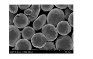
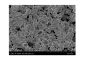
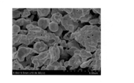
- 4 is an image obtained by photographing the surface of a silver powder (2-1) in an example using a scanning electron microscope (magnification: 1000 times).
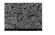
- 5 is an image obtained by photographing the surface of a silver powder (2-2) in an example with a scanning electron microscope (magnification: 1000 times).
- 5 is an image obtained by photographing the surface of a silver powder (2-3) in an example with a scanning electron microscope (magnification: 1000 times).
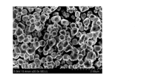
- 4 is an image obtained by photographing the surface of a silver powder (2-4) in an example with a scanning electron microscope (magnification: 20000 times).
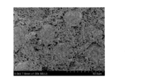
- 9 is an image obtained by photographing the surface of a wiring made of the sintered body of Example 3 with a scanning electron microscope (magnification: 1000 times).
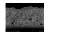
- 9 is an image obtained by photographing a cross section of a wiring made of the sintered body of Example 3 with a scanning electron microscope (magnification: 700 times).
- 9 is an image obtained by photographing the surface of a wiring formed of the sintered body of Example 3 with a scanning electron microscope (magnification: 5000 times).
- 9 is an image obtained by photographing the surface of a wiring made of the sintered body of Example 3 with a scanning electron microscope (magnification: 10000 times).
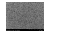
- 9 is an image obtained by photographing the surface of a wiring formed of the sintered body of Comparative Example 3 with a scanning electron microscope (magnification: 1000 times).
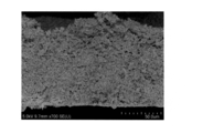
- 9 is an image obtained by photographing a cross section of a wiring made of the sintered body of Comparative Example 3 with a scanning electron microscope (magnification: 700 times).
- 11 is an image obtained by photographing the surface of a wiring formed of the sintered body of Comparative Example 3 with a scanning electron microscope (magnification: 5000 times).
- 11 is an image obtained by photographing the surface of a wiring formed of the sintered body of Comparative Example 3 with a scanning electron microscope (magnification: 10000 times).
- 13 is an image obtained by photographing the surface of a wiring formed of the sintered body of Comparative Example 7 with a scanning electron microscope (400 times magnification).
- 11 is an image obtained by photographing the surface of a wiring formed of the sintered body of Comparative Example 7 with a scanning electron microscope (magnification: 1000 times).
- 6 is an image obtained by photographing a cross section of a sample for measuring shear strength after sintering in Example 3 by using a scanning electron microscope (magnification: 1000 times).
- 5 is an image obtained by photographing a cross section of a sample for measuring shear strength after sintering in Example 3 by using a scanning electron microscope (magnification: 2500 times).
- 9 is an image obtained by photographing a cross section of a sample for measuring shear strength after sintering in Comparative Example 3 with a scanning electron microscope (magnification: 1000 times).
- 9 is an image obtained by photographing a cross section of a sample for measuring shear strength after sintering of Comparative Example 3 by using a scanning electron microscope (magnification: 2500 times).
- the conductive paste of the present invention comprises a flake silver powder having a median diameter D50 of 15 ⁇ m or less, a silver powder having a median diameter D50 of 25 ⁇ m or more, and a solvent, and the flake silver powder and a silver powder having a median diameter D50 of 25 ⁇ m or more.
- the content of the flake silver powder is 15 to 70 parts by mass, and the content of the silver powder having a median diameter D50 of 25 ⁇ m or more is 30 to 85 parts by mass with respect to the total of 100 parts by mass.
- the median diameter D50 of the flake silver powder is 15 ⁇ m or less, preferably 0.1 ⁇ m to 15 ⁇ m, more preferably 2 ⁇ m to 10 ⁇ m.
- the surface area increases as compared with the case where the spherical powder is used, so that a sintered body is easily formed.
- the median diameter D50 of each silver powder means a value measured by a laser diffraction method using SALD-2300 (manufactured by Shimadzu Corporation).
- the flake-like silver powder may be any as long as a majority of particles constituting the silver powder can be recognized as a flake (flake or flake) under a microscope. Typically, it means that 51% by mass or more of the particles (primary particles) constituting the silver powder have a flake (flake or flake) shape.
- the flake-like (flake-like or flake-like) particles mean particles having an aspect ratio (ratio of longest major axis / shortest minor axis) of 5 to 300.
- the silver powder having a median diameter D50 of 25 ⁇ m or more has a median diameter D50 of 25 ⁇ m or more, preferably 25 ⁇ m to 100 ⁇ m, and more preferably 30 ⁇ m to 80 ⁇ m.
- the current flows along each particle, so that the number of contact points of the particles increases and the overall resistivity increases.
- the median diameter of the silver powder having a median diameter D50 of 25 ⁇ m or more is within the above numerical range, one particle contains large particles, so that the number of contact points of the particles can be reduced, and the overall resistivity decreases. . Therefore, a conductive paste having a lower electric resistance value and a higher conductivity when a sintered body is obtained than when only a particle size of less than 25 ⁇ m is used is obtained.
- the shape of the silver powder having a median diameter D50 of 25 ⁇ m or more is not particularly limited, but may be spherical or non-spherical.
- non-spherical, flake-like, needle-like, horn-like, dendritic, granular, irregular, teardrop-like, plate-like, ultra-thin plate-like, hexagonal plate-like, columnar, rod-like, porous, fibrous, Lumped, spongy, horned, rounded and the like are preferable.
- the content of the flaky silver powder is 15 to 70 parts by mass, preferably 30 to 60 parts by mass, and more preferably 30 to 50 parts by mass based on 100 parts by mass of the total of the flaky silver powder and the silver powder having a median diameter D50 of 25 ⁇ m or more. More preferred.
- the content of the silver powder having a median diameter D50 of 25 ⁇ m or more based on 100 parts by mass of the total of the flaky silver powder and the silver powder having a median diameter D50 of 25 ⁇ m or more is 30 to 85 parts by mass, preferably 40 to 70 parts by mass. 50 to 70 parts by mass is more preferred.
- the sintered body has a low electric resistance value, excellent electrical conductivity, and high electron conductivity.
- a conductive paste having excellent bonding strength when bonding substrates and the like is obtained.
- the content of the flaky silver powder with respect to 100 parts by mass of the conductive paste is preferably 10 to 50 parts by mass, more preferably 20 to 50 parts by mass, and most preferably 30 to 50 parts by mass. If the content of the flake silver powder is less than 10 parts by mass with respect to 100 parts by mass of the conductive paste, it is difficult to make the composition containing the flake silver powder into a paste. Further, even if the composition containing the flake silver powder can be made into a paste, the sintered body obtained from such a conductive paste has a high electric resistance value and is inferior in conductivity.
- the content of the silver powder having a median diameter D50 of 25 ⁇ m or more based on 100 parts by mass of the conductive paste is preferably 15 to 60 parts by mass, more preferably 20 to 55 parts by mass, and most preferably 30 to 55 parts by mass.
- the content of the silver powder having a median diameter D50 of 25 ⁇ m or more is within the above-mentioned numerical range, the electrical resistance of the sintered body is low, the electrical conductivity is low, and the bonding strength when an electronic substrate or the like is bonded is improved. An excellent conductive paste is obtained.
- Examples of the solvent include water, alcohol solvents, glycol ether solvents, terpineols, and the like.
- Examples of alcohol solvents include isopropyl alcohol, 1,2-butanediol, isobornylcyclohexanol, 2,4-diethyl-1,5-pentanediol, 2,2-dimethyl-1,3-propanediol, 2,5 -Dimethyl-2,5-hexanediol, 2,5-dimethyl-3-hexyne-2,5-diol, 2,3-dimethyl-2,3-butanediol, 1,1,1-tris (hydroxymethyl) Ethane, 2-ethyl-2-hydroxymethyl-1,3-propanediol, 2,2'-oxybis (methylene) bis (2-ethyl-1,3-propanediol), 2,2-bis (hydroxymethyl) 1,3-propanediol, 1,2,6-trihydroxyhe
- glycol ether solvent examples include diethylene glycol mono-2-ethylhexyl ether, ethylene glycol monophenyl ether, 2-methylpentane-2,4-diol, diethylene glycol monohexyl ether, diethylene glycol dibutyl ether, and triethylene glycol monobutyl ether.
- the content of the solvent with respect to 100 parts by mass of the conductive paste is preferably 2 to 20 parts by mass, more preferably 2 to 15 parts by mass, and most preferably 5 to 10 parts by mass.
- the content of the solvent is within the above numerical range, a paste having good coatability can be obtained.
- the conductive paste of the present invention has a flaky silver powder having a median diameter D50 of 15 ⁇ m or less, a silver powder having a median diameter D50 of 25 ⁇ m or more, and a bimodal powder having peaks at 0.1 ⁇ m to 0.5 ⁇ m and 1 ⁇ m to 15 ⁇ m.
- Silver powder having a particle size distribution, and a solvent the flake silver powder, silver powder having a median diameter D50 of 25 ⁇ m or more, and a total of 100 parts by mass of the silver powder having a bimodal particle size distribution, the flake-like
- the content of silver powder is 8 to 55 parts by mass
- the content of silver powder having a median diameter D50 of 25 ⁇ m or more is 15 to 65 parts by mass
- the content of silver powder having a bimodal particle size distribution is 4 parts by mass. 4545 parts by mass.
- Median diameter D50 of flake silver powder, definition of flake shape, content of flake silver powder with respect to 100 parts by mass of conductive paste, median diameter D50 and shape of silver powder having median diameter D50 of 25 ⁇ m or more, with respect to 100 parts by mass of conductive paste As the content of silver powder having a median diameter D50 of 25 ⁇ m or more, the type of solvent, and the content of solvent with respect to 100 parts by mass of the conductive paste, those described in the first embodiment can be used.
- a silver powder having a bimodal particle size distribution has peaks at 0.1 ⁇ m to 0.5 ⁇ m and 1 ⁇ m to 15 ⁇ m, and preferably has peaks at 0.1 ⁇ m to 0.3 ⁇ m and 3 ⁇ m to 10 ⁇ m.
- the bimodal particle size distribution means a value measured by a laser diffraction method using SALD-2300 (manufactured by Shimadzu Corporation).
- the shape of the silver powder having a bimodal particle size distribution is not particularly limited, but may be spherical or non-spherical.
- non-spherical, flake-like, needle-like, horn-like, dendritic, granular, irregular, teardrop-like, plate-like, ultra-thin plate-like, hexagonal plate-like, columnar, rod-like, porous, fibrous, Lumped, spongy, horned, rounded and the like are examples of such shapes.
- the shape of the silver powder having a bimodal particle size distribution is spherical
- the shape is not limited to a true spherical shape, and any shape may be used as long as the majority of the particles constituting the silver powder are recognized as spherical under a microscope.
- it means that 80% by mass or more of the particles (primary particles) constituting the silver powder have a spherical shape or a shape similar thereto.
- the spherical particles mean particles having an aspect ratio (ratio of major axis / minor axis) of 1.0 to 1.3.
- the content of the flake silver powder is 8 to 55 parts by mass, and 15 to 40 parts by mass with respect to 100 parts by mass of the total of the flake silver powder, the silver powder having a median diameter D50 of 25 ⁇ m or more, and the silver powder having a bimodal particle size distribution. Parts by mass, more preferably 20 to 35 parts by mass.
- the content of the silver powder having a median diameter D50 of 25 ⁇ m or more based on a total of 100 parts by mass of the flake silver powder, the silver powder having a median diameter D50 of 25 ⁇ m or more, and the silver powder having a bimodal particle size distribution is 15 to 65 parts by mass.
- the amount is preferably 20 to 65 parts by mass, more preferably 30 to 60 parts by mass.
- the content of the silver powder having a bimodal particle size distribution with respect to a total of 100 parts by mass of the flaky silver powder, the silver powder having a median diameter D50 of 25 ⁇ m or more, and the silver powder having a bimodal particle size distribution is 4 to 45 parts by mass. And preferably 10 to 40 parts by mass, more preferably 15 to 30 parts by mass.
- the sintered body When the content of the flake silver powder, the content of the silver powder having a median diameter D50 of 25 ⁇ m or more, and the content of the silver powder having a bimodal particle size distribution were all within the above numerical ranges, the sintered body was obtained. In this case, a conductive paste having a low electric resistance value, excellent conductivity, and excellent joining strength when an electronic substrate or the like is joined can be obtained.
- the content of silver powder having a bimodal particle size distribution with respect to 100 parts by mass of the conductive paste is preferably 5 to 40 parts by mass, more preferably 10 to 35 parts by mass, and most preferably 10 to 30 parts by mass.
- the conductive paste of the present invention is prepared by using ARV-310 (manufactured by Sinky Co., Ltd.) using flake silver powder, silver powder having a median diameter D50 of 25 ⁇ m or more, a solvent, and optionally silver powder having a bimodal particle size distribution. ) It can be kneaded and manufactured using an apparatus.
- the present invention provides a sintered body obtained by sintering the above conductive paste.
- a sintered body can be obtained by printing or applying a conductive paste on a substrate and then sintering. Since such a sintered body has conductivity, it functions as a wiring (electronic circuit) on a substrate.
- the method of printing or applying the conductive paste is not particularly limited, and examples thereof include dispense application, print application, spray application, brushing, and injection.
- the substrate on which the sintered body is provided is not particularly limited, but a glass fiber reinforced epoxy printed board such as FR4 having high heat resistance, a polyimide-based board, a ceramic such as DBA (Direct Bonded Aluminum) or DBC (Direct Bonded Copper).
- a glass fiber reinforced epoxy printed board such as FR4 having high heat resistance
- a polyimide-based board such as DBA (Direct Bonded Aluminum) or DBC (Direct Bonded Copper).
- DBA Direct Bonded Aluminum
- DBC Direct Bonded Copper
- Substrates, metal substrates such as copper, silver, and aluminum, and Cu lead frames are exemplified. Electronic components are mounted on the substrate.
- the metal substrate may be plated with metal. Examples of the metal used for metal plating include gold, silver, nickel, and tin.
- the conditions for sintering the conductive paste are not particularly limited, but the heating temperature in sintering is preferably 150 to 350 ° C, more preferably 180 to 300 ° C, and most preferably 200 to 300 ° C.
- the heating time in sintering is preferably from 10 to 60 minutes, more preferably from 15 to 45 minutes, and most preferably from 20 to 30 minutes. No pressure is applied to the conductive paste during sintering.
- the sintering can be performed in an air atmosphere or an atmosphere having an oxygen concentration of 1% or more.
- the shape of the sintered body is not particularly limited, and examples thereof include a sheet, a film, a tape, a line, a disk, a block, a spot, and an irregular shape.
- the sintered body of the present invention can achieve an electric resistance value of 8.5 ⁇ ⁇ cm or less.
- the electric resistance value of the sintered body can be measured by the method described in “(1) Evaluation of electric resistance value” of (Evaluation) described later.
- the present invention provides a sintered body obtained by sintering a laminate including a substrate, the above-mentioned conductive paste, and a conductor.
- a laminate can be manufactured by sequentially laminating a conductive paste and a conductor on a substrate. Then, a sintered body can be obtained by sintering the laminate. In such a sintered body, a portion derived from the conductive paste has conductivity and bonds the substrate and the conductor, and thus functions as a conductive bonding portion (adhesion portion).
- the substrate to be bonded include a circuit substrate, a glass fiber reinforced epoxy-based printed substrate, a polyimide-based substrate, a ceramic substrate, a metal substrate, a Cu lead frame, and the like.
- Examples of the conductor to be bonded include chip components such as a capacitor and a resistor, a chip obtained by forming a semiconductor element such as a resistor, a transistor, a capacitor, and an integrated circuit on a wafer and then cutting a section of each semiconductor element from the wafer. Is mentioned.
- Conditions for sintering the above-mentioned laminated body differ depending on an object to be joined.
- the conditions are as follows. The conditions under an air atmosphere are mentioned.
- the above laminated body after sintering can achieve a shear strength of 25 MPa or more.
- the shear strength means a value measured by a method in accordance with JIS Z 3198, and the bonding strength (shear strength) of the laminated body after sintering is described in “(2) of (Evaluation) described later. Evaluation of Shear Strength ".
- Example 1 (1) Evaluation of Electric Resistance
- the conductive pastes of Examples 1 to 11 and Comparative Examples 1 to 13 were applied to a glass substrate (2 mm in thickness) by screen printing using a metal mask (100 ⁇ m in thickness).
- the glass substrate to which the conductive paste was applied was heated at 200 ° C. for 30 minutes under atmospheric pressure and atmospheric pressure, and sintering was performed to form wiring.
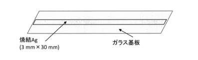
- the wiring by the sintered body of the conductive paste thus obtained was 3 mm ⁇ 30 mm in length ⁇ width.
- FIG. 1 shows a schematic diagram of the obtained wiring.
- a copper substrate (length ⁇ width: 50 mm ⁇ 50 mm) in which a Ti layer (thickness: 40 nm) and an Ag layer (thickness: 1000 nm) are laminated in order from the copper substrate side (hereinafter, a test piece) (Referred to as (1)).
- the conductive pastes of Examples 1 to 11 and Comparative Examples 1 to 13 were screen-printed on the Ag layer of the test piece (1) using a metal mask (thickness: 100 ⁇ m).
- a Si chip (length ⁇ width: 3 mm ⁇ 3 mm) in which a Ti layer (thickness: 40 nm) and an Ag layer (thickness: 1000 nm) are laminated by sputtering in order from the Si chip side (hereinafter, referred to as a test piece (2)) was prepared.
- Example 1 to 3 and 5 to 11 and Comparative Examples 1 to 3 and 5 to 13 a chip mounter (product name SMT-64RH, product name) was placed on the conductive paste applied to the test piece (1).
- the Ag layer side of the test piece (2) was laminated using Okuhara Electric Co., Ltd. to obtain a sample including the test piece (1), the conductive paste, and the test piece (2).
- the obtained sample was heated at 200 ° C. for 30 minutes under atmospheric pressure and atmospheric pressure to perform sintering.
- Example 4 and Comparative Example 4 using ethanol as a solvent when a chip mounter was used, the solvent was volatilized before the test piece (2) was laminated on the conductive paste, and the test piece (2) was used.
- Example 4 shows a schematic diagram of the obtained sample after sintering.
- Example 1 to 11 Comparative Examples 1 to 13
- a commercially available product name AgC239 manufactured by Fukuda Metal Foil & Powder Co., Ltd., median diameter D50: 2.5 ⁇ m, flake shape
- silica powder (1) a commercially available product name AgC239 (manufactured by Fukuda Metal Foil & Powder Co., Ltd., median diameter D50: 2.5 ⁇ m, flake shape)
- silver powder (2-1) two types of silver powder having a median diameter D50 of 25 ⁇ m or more
- siver powder (2-2) two types of silver powder having a median diameter D50 of 25 ⁇ m or more
- silver powder (2-2) a silver powder having a median diameter D50 of less than 25 ⁇ m
- silver powder (2-4) silver powder having a particle size distribution of 300 to 700 nm
- silver powder (3) silver powder having a bimodal particle size distribution
- Spherical silver powder having a median diameter D50: 36.34 ⁇ m was obtained by heating silver to a molten state, spraying the molten silver, and cooling (melt spraying method). 2-1) was prepared.
- Silver powder having a peak at 300 to 700 nm was produced by the following production method. First, 1.0 g of silver nitrate (silver compound) was dissolved in 50 g of ethylene glycol (polyhydric alcohol). Next, 0.5 g of polyvinylpyrrolidone (dispersant) was dispersed in ethylene glycol. Next, after the ethylene glycol was heated to 150 ° C. (reaction temperature), the reaction was carried out for 1 hour while stirring at a rotation speed of 500 rpm while maintaining the reaction temperature at 150 ° C. The silver powder after the reaction was separated from ethylene glycol (polyhydric alcohol) using a metal mesh, and the separated silver powder was washed with ethanol to obtain silver powder (2-4).
- 3A to 3D show images of the obtained silver powders (2-1) to (2-4) taken by a field emission scanning electron microscope (FE-SEM) (JSM-7000F manufactured by JEOL Ltd.).
- 3A to 3C are photographs of the surfaces of the silver powders (2-1) to (2-3) at a magnification of 1000 times
- FIG. 3D is a photograph of the surfaces of the silver powders (2-4) at a magnification of 20000 times. It was done.
- silver powder (2) the silver powders (2-1) to (2-4) are collectively referred to as silver powder (2).
- Silver powder (3) having a bimodal particle size distribution having peaks at 0.1 ⁇ m to 0.5 ⁇ m and 1 ⁇ m to 15 ⁇ m was produced by the following production method.
- silver powder A was produced by exactly the same production method as silver powder (2-4). Then, while stirring 50 g of ethylene glycol at a rotation speed of 500 rpm, 2.0 g of silver nitrate was dissolved in ethylene glycol, and then 0.05 g of silver powder A was further dispersed in ethylene glycol. Next, after the ethylene glycol was heated to 150 ° C. (reaction temperature), the reaction was carried out for 1 hour while stirring at a rotation speed of 500 rpm while maintaining the reaction temperature at 150 ° C. Thereafter, the silver powder after the reaction was separated from ethylene glycol using a metal mesh, and the separated silver powder was washed with ethanol to obtain silver powder (3).
- the median diameter D50 of the silver powders (1) and (2-1) to (2-3) and the particle size distribution of the silver powder (2-4) and the silver powder (3) used in this example and the comparative example are SALD- 2300 (manufactured by Shimadzu Corporation) was measured by a laser diffraction method.
- the conductive pastes of Examples 1 to 11 each contained flake silver powder having a median diameter D50 of 15 ⁇ m or less, silver powder having a median diameter D50 of 25 ⁇ m or more, and a solvent, and contained the flake silver powder and the median diameter D50 of 25 ⁇ m or more.
- the content of the flaky silver powder is 15 to 70 parts by mass, and the content of the silver powder having a median diameter D50 of 25 ⁇ m or more is 30 to 85 parts by mass with respect to a total of 100 parts by mass of the silver powder having It is a conductive paste.
- the electric resistance value of the wiring made of the sintered body is low, and has better conductivity, and the sintered body has excellent shear strength and has better jointability.
- the content of the flake silver powder was 30 to 42 parts by mass with respect to the total of 100 parts by mass of the flake silver powder and the silver powder having a median diameter D50 of 25 ⁇ m or more, and the median diameter of 25 ⁇ m or more was used.
- Comparative Example 1 shown in Table 2 above is a conductive paste containing no silver powder (1) and silver powder (2).
- Comparative Examples 2 to 4 and 10 are conductive pastes containing no silver powder (2).
- Comparative Examples 7 and 9 are conductive pastes containing no silver powder (1).
- Comparative Examples 5 and 8 contain both the silver powder (1) and the silver powder (2-1), but the silver powder (1) was added to the silver powder (1) and the silver powder (2-1) in a total of 100 parts by mass.
- the conductive paste has a content of less than 15 parts by mass and a silver powder (2-1) content of more than 85 parts by mass.
- Comparative Example 6 contained both silver powder (1) and silver powder (2-1), but the content of silver powder (1) was 100 parts by mass in total of silver powder (1) and silver powder (2). Is more than 70 parts by mass and the content of silver powder (2-1) is less than 30 parts by mass.
- Comparative Examples 11 to 13 are conductive pastes containing no silver powder and having a median diameter D50 of 25 ⁇ m or more.
- the conductive pastes of Comparative Examples 1 to 5, 7 to 10, and 13 have a lower electric resistance value of the wiring made of the sintered body than the conductive pastes of Examples 1 to 13. It was high, the conductivity was insufficient, and the shear strength of the sintered body was low, and the bondability was poor.
- the conductive paste of Comparative Example 6 although the sintered body had good bonding properties, the electrical resistance of the wiring formed by the sintered body was high and the conductivity was insufficient.
- the wiring of the sintered body had good conductivity, but the shear strength of the sintered body was low and the bonding property was poor.
- 4A to 6B show images of the wirings of the sintered bodies of Example 3 and Comparative Examples 3 and 7 taken by a field emission scanning electron microscope (FE-SEM) (JSM-7000F manufactured by JEOL).
- 4A, 4C, and 4D are photographs of the surface of the wiring of Example 3 at magnifications of 1,000, 5,000, and 10,000, respectively.
- FIG. 4B is a photograph of a cross section of the wiring of Example 3 taken at a magnification of 700 times.
- 5A, 5C, and 5D are photographs of the surface of the wiring of Comparative Example 3 at magnifications of 1,000, 5,000, and 10,000, respectively.
- FIG. 5B is a photograph of a cross section of the wiring of Comparative Example 3 taken at a magnification of 700 times.
- 6A and 6B are photographs of the surface of the wiring of Comparative Example 7 at magnifications of 400 and 1000, respectively.
- Example 3 in the wiring of Example 3, the silver powder (1) having a small diameter and a flaky silver powder (2-1), the silver powder having a large diameter (2-1), and the silver powder (3) having a small diameter and a bimodal particle size distribution were obtained. ) Were observed in the sintered body. Then, in the wiring of Example 3, it was found that the flake silver particles and the silver particles having a small diameter and the silver particles having a large diameter were sufficiently in contact with each other and fused. As a result, it is considered that in the wiring of Example 3, the moving speed of the electrons in the wiring was increased, and the electric resistance was reduced.
- the wiring of Comparative Example 3 in the wiring of Comparative Example 3, the structures derived from the flake silver powder (1) having a small diameter and the silver powder (3) having a small diameter and a bimodal particle size distribution were respectively sintered. Observed in the body.
- the wiring of Comparative Example 3 is composed of only the silver powders (1) and (3) having a small diameter and does not include the silver powder (2-1) or (2-2) having a large diameter. It was found that the silver particles were not sufficiently in contact with each other and were not sufficiently fused in other portions, although they were in some contact. Thus, it is considered that the electrical resistance of the wiring of Comparative Example 3 was higher than that of the wiring of Example 3.
- the wiring of Comparative Example 7 is composed of only the large-diameter silver powder (2-1) and does not include the small-diameter silver powders (1) and (3). It was found that silver particles existed independently and hardly fused together. Thus, it is considered that the electrical resistance value of the wiring of Comparative Example 7 was extremely high.
- 7A to 8B show images of the samples for measuring the shear strength after sintering of Example 3 and Comparative Example 3 taken by a field emission scanning electron microscope (FE-SEM) (JSM-7000F manufactured by JEOL). Show. 7A and 7B are cross-sectional images of the sample of Example 3 taken at magnifications of 1000 and 2500, respectively. 8A and 8B are cross-sectional images of the sample of Comparative Example 3 taken at magnifications of 1000 and 2500, respectively.
- FE-SEM field emission scanning electron microscope
- the sample of Comparative Example 3 is composed of only the small-diameter silver powders (1) and (3) and does not include the large-diameter silver powder (2-1) or (2-2). Therefore, it was found that the contact area between the silver particles was small and did not sufficiently fuse, so that there were many voids inside the sintered body. Thus, it is considered that the shear strength of the sample of Comparative Example 3 was lower than that of the sample of Example 3.
- the flake silver powder having a median diameter D50 of 15 ⁇ m or less, the silver powder having a median diameter D50 of 25 ⁇ m or more, and a solvent, the flake silver powder and the median diameter D50 of 25 ⁇ m or more are included.
Landscapes
- Chemical & Material Sciences (AREA)
- Dispersion Chemistry (AREA)
- Engineering & Computer Science (AREA)
- Microelectronics & Electronic Packaging (AREA)
- Physics & Mathematics (AREA)
- Spectroscopy & Molecular Physics (AREA)
- Materials Engineering (AREA)
- Mechanical Engineering (AREA)
- Metallurgy (AREA)
- Organic Chemistry (AREA)
- Conductive Materials (AREA)
- Powder Metallurgy (AREA)
- Non-Insulated Conductors (AREA)
- Parts Printed On Printed Circuit Boards (AREA)
- Die Bonding (AREA)
Abstract
Le but de l'invention est de fournir : une pâte conductrice qui, lorsqu'elle est constituée sous la forme d'un corps fritté, présente une faible valeur de résistance électrique et une excellente conductivité; et un corps fritté de la pâte conductrice. La pâte conductrice se caractérise en ce qu'elle contient : une poudre d'argent lamellaire ayant un diamètre moyen D50 d'au plus 15 µm, une poudre d'argent ayant un diamètre moyen D50 d'au moins 25 µm, et un solvant; et que, par rapport à 100 parties en masse du total de la poudre d'argent lamellaire et de la poudre d'argent ayant un diamètre moyen D50 d'au moins 25 µm, la teneur en poudre d'argent lamellaire est de 15 à 70 parties en masse et la teneur de la poudre d'argent ayant un diamètre moyen D50 d'au moins 25 µm est de 30 à 85 parties en masse.
Priority Applications (5)
| Application Number | Priority Date | Filing Date | Title |
|---|---|---|---|
| JP2020528691A JP6756085B2 (ja) | 2018-07-06 | 2019-03-20 | 導電性ペースト及び焼結体 |
| EP19830980.9A EP3806111B1 (fr) | 2018-07-06 | 2019-03-20 | Pâte conductrice electrique et corps fritté |
| US17/258,271 US11710580B2 (en) | 2018-07-06 | 2019-03-20 | Electrically conductive paste and sintered body |
| CN201980039267.2A CN112272851B (zh) | 2018-07-06 | 2019-03-20 | 导电性糊料和烧结体 |
| EP22193544.8A EP4148748B1 (fr) | 2018-07-06 | 2019-03-20 | Pâte conductrice electrique et corps fritté |
Applications Claiming Priority (2)
| Application Number | Priority Date | Filing Date | Title |
|---|---|---|---|
| JP2018-129163 | 2018-07-06 | ||
| JP2018129163 | 2018-07-06 |
Publications (1)
| Publication Number | Publication Date |
|---|---|
| WO2020008689A1 true WO2020008689A1 (fr) | 2020-01-09 |
Family
ID=69060536
Family Applications (1)
| Application Number | Title | Priority Date | Filing Date |
|---|---|---|---|
| PCT/JP2019/011634 Ceased WO2020008689A1 (fr) | 2018-07-06 | 2019-03-20 | Pâte conductrice et corps fritté |
Country Status (6)
| Country | Link |
|---|---|
| US (1) | US11710580B2 (fr) |
| EP (2) | EP3806111B1 (fr) |
| JP (1) | JP6756085B2 (fr) |
| CN (1) | CN112272851B (fr) |
| TW (1) | TWI729373B (fr) |
| WO (1) | WO2020008689A1 (fr) |
Cited By (3)
| Publication number | Priority date | Publication date | Assignee | Title |
|---|---|---|---|---|
| JP2021091819A (ja) * | 2019-12-12 | 2021-06-17 | スタンレー電気株式会社 | 焼結用インク、その製造方法、金属粒子、その製造方法、および、回路基板の製造方法 |
| CN113168931A (zh) * | 2020-06-24 | 2021-07-23 | 千住金属工业株式会社 | 导电性糊料、层叠体及Cu基板或Cu电极与导电体的接合方法 |
| WO2021260960A1 (fr) | 2020-06-24 | 2021-12-30 | 千住金属工業株式会社 | Pâte conductrice, corps stratifié, procédé de liaison de stratifié de cuivre/électrode de cuivre et conducteur |
Families Citing this family (1)
| Publication number | Priority date | Publication date | Assignee | Title |
|---|---|---|---|---|
| EP4324578B1 (fr) * | 2022-08-17 | 2024-10-09 | Heraeus Electronics GmbH & Co. KG | Pâte de frittage d'argent et son utilisation pour relier des composants |
Citations (5)
| Publication number | Priority date | Publication date | Assignee | Title |
|---|---|---|---|---|
| JPH0581923A (ja) | 1991-01-31 | 1993-04-02 | Fukuda Metal Foil & Powder Co Ltd | 導電性接着剤 |
| JP2004362950A (ja) | 2003-06-05 | 2004-12-24 | Noritake Co Ltd | 銀粉末を主体とする導体ペースト及びその製造方法 |
| WO2007034833A1 (fr) | 2005-09-21 | 2007-03-29 | Nihon Handa Co., Ltd. | Composition particulaire d'argent pateuse, processus de production d'argent massif, argent massif, procede d'assemblage, et processus de production d'une carte imprimee |
| JP2009170277A (ja) | 2008-01-17 | 2009-07-30 | Osaka Univ | 導電性ペースト |
| JP2012028250A (ja) * | 2010-07-27 | 2012-02-09 | Jsr Corp | 導電性ペースト組成物および導電接着方法 |
Family Cites Families (10)
| Publication number | Priority date | Publication date | Assignee | Title |
|---|---|---|---|---|
| US6814795B2 (en) * | 2001-11-27 | 2004-11-09 | Ferro Corporation | Hot melt conductor paste composition |
| JP4790238B2 (ja) | 2004-08-27 | 2011-10-12 | 鬼怒川ゴム工業株式会社 | 導電性弾性体組成物 |
| JP5281529B2 (ja) | 2009-09-28 | 2013-09-04 | 京都エレックス株式会社 | 加熱硬化型導電性ペースト組成物およびその導電性ペースト組成物を用いた電極並びに配線パターンの形成方法 |
| KR20130124482A (ko) * | 2010-09-01 | 2013-11-14 | 페로 코포레이션 | 태양열 적용을 위한 비아 충전 물질 |
| US8419981B2 (en) * | 2010-11-15 | 2013-04-16 | Cheil Industries, Inc. | Conductive paste composition and electrode prepared using the same |
| WO2012133627A1 (fr) * | 2011-03-31 | 2012-10-04 | 戸田工業株式会社 | Poudre de cuivre recouverte d'argent et procédé de production de cette dernière, pâte conductrice qui contient une poudre de cuivre recouverte d'argent, agent adhésif conducteur, film conducteur et circuit électrique |
| CN103000248B (zh) * | 2012-11-10 | 2015-10-28 | 江苏瑞德新能源科技有限公司 | 一种适应高方阻浅结的太阳能电池正银浆料用粉体料 |
| US8828536B2 (en) * | 2013-02-04 | 2014-09-09 | Eastman Kodak Company | Conductive article having silver nanoparticles |
| WO2016007351A1 (fr) | 2014-07-11 | 2016-01-14 | E. I. Du Pont De Nemours And Company | Compositions fluides durcissant a basse temperature pour former des trajets thermiquement conducteurs dans des applications de type electronique, et procedes correspondants |
| WO2017091782A1 (fr) | 2015-11-24 | 2017-06-01 | Plant Pv, Inc | Empilements multicouches cuits pour circuits intégrés et cellules solaires |
-
2019
- 2019-03-20 WO PCT/JP2019/011634 patent/WO2020008689A1/fr not_active Ceased
- 2019-03-20 JP JP2020528691A patent/JP6756085B2/ja active Active
- 2019-03-20 US US17/258,271 patent/US11710580B2/en active Active
- 2019-03-20 EP EP19830980.9A patent/EP3806111B1/fr active Active
- 2019-03-20 EP EP22193544.8A patent/EP4148748B1/fr active Active
- 2019-03-20 CN CN201980039267.2A patent/CN112272851B/zh active Active
- 2019-04-01 TW TW108111518A patent/TWI729373B/zh active
Patent Citations (5)
| Publication number | Priority date | Publication date | Assignee | Title |
|---|---|---|---|---|
| JPH0581923A (ja) | 1991-01-31 | 1993-04-02 | Fukuda Metal Foil & Powder Co Ltd | 導電性接着剤 |
| JP2004362950A (ja) | 2003-06-05 | 2004-12-24 | Noritake Co Ltd | 銀粉末を主体とする導体ペースト及びその製造方法 |
| WO2007034833A1 (fr) | 2005-09-21 | 2007-03-29 | Nihon Handa Co., Ltd. | Composition particulaire d'argent pateuse, processus de production d'argent massif, argent massif, procede d'assemblage, et processus de production d'une carte imprimee |
| JP2009170277A (ja) | 2008-01-17 | 2009-07-30 | Osaka Univ | 導電性ペースト |
| JP2012028250A (ja) * | 2010-07-27 | 2012-02-09 | Jsr Corp | 導電性ペースト組成物および導電接着方法 |
Non-Patent Citations (1)
| Title |
|---|
| See also references of EP3806111A4 |
Cited By (10)
| Publication number | Priority date | Publication date | Assignee | Title |
|---|---|---|---|---|
| JP2021091819A (ja) * | 2019-12-12 | 2021-06-17 | スタンレー電気株式会社 | 焼結用インク、その製造方法、金属粒子、その製造方法、および、回路基板の製造方法 |
| CN113168931A (zh) * | 2020-06-24 | 2021-07-23 | 千住金属工业株式会社 | 导电性糊料、层叠体及Cu基板或Cu电极与导电体的接合方法 |
| KR102307809B1 (ko) | 2020-06-24 | 2021-09-30 | 센주긴조쿠고교 가부시키가이샤 | 도전성 페이스트, 적층체, 및 Cu 기판 또는 Cu 전극과 도전체와의 접합 방법 |
| WO2021260960A1 (fr) | 2020-06-24 | 2021-12-30 | 千住金属工業株式会社 | Pâte conductrice, corps stratifié, procédé de liaison de stratifié de cuivre/électrode de cuivre et conducteur |
| US11278955B2 (en) | 2020-06-24 | 2022-03-22 | Senju Metal Industry Co., Ltd. | Electrically conductive paste, laminated body, and method for bonding Cu substrate or Cu electrode to electrical conductor |
| EP3958279A4 (fr) * | 2020-06-24 | 2022-09-14 | Senju Metal Industry Co., Ltd | Pâte conductrice, corps stratifié, procédé de liaison de stratifié de cuivre/électrode de cuivre et conducteur |
| EP4279264A2 (fr) | 2020-06-24 | 2023-11-22 | Senju Metal Industry Co., Ltd. | Pâte conductrice, corps stratifié, procédé de liaison de stratifié de cuivre/électrode de cuivre et conducteur |
| EP4279265A2 (fr) | 2020-06-24 | 2023-11-22 | Senju Metal Industry Co., Ltd. | Pâte conductrice, corps stratifié, procédé de liaison de stratifié de cuivre/électrode de cuivre et conducteur |
| EP4279264A3 (fr) * | 2020-06-24 | 2024-02-21 | Senju Metal Industry Co., Ltd. | Pâte conductrice, corps stratifié, procédé de liaison de stratifié de cuivre/électrode de cuivre et conducteur |
| EP4279265A3 (fr) * | 2020-06-24 | 2024-02-21 | Senju Metal Industry Co., Ltd. | Pâte conductrice, corps stratifié, procédé de liaison de stratifié de cuivre/électrode de cuivre et conducteur |
Also Published As
| Publication number | Publication date |
|---|---|
| EP3806111A4 (fr) | 2021-08-11 |
| US20210245242A1 (en) | 2021-08-12 |
| EP4148748B1 (fr) | 2025-07-09 |
| TWI729373B (zh) | 2021-06-01 |
| TW202006749A (zh) | 2020-02-01 |
| JPWO2020008689A1 (ja) | 2020-12-17 |
| EP3806111B1 (fr) | 2024-03-13 |
| CN112272851A (zh) | 2021-01-26 |
| US11710580B2 (en) | 2023-07-25 |
| EP4148748A1 (fr) | 2023-03-15 |
| EP3806111A1 (fr) | 2021-04-14 |
| CN112272851B (zh) | 2022-03-01 |
| JP6756085B2 (ja) | 2020-09-16 |
Similar Documents
| Publication | Publication Date | Title |
|---|---|---|
| JP4353380B2 (ja) | ペースト状銀粒子組成物、固形状銀の製造方法、固形状銀、接合方法およびプリント配線板の製造方法 | |
| JP6756085B2 (ja) | 導電性ペースト及び焼結体 | |
| EP3598461A1 (fr) | Dispersion, procédé de production d'une structure équipée d'un motif conducteur en utilisant une dispersion, et structure équipée d'un motif conducteur | |
| US11278955B2 (en) | Electrically conductive paste, laminated body, and method for bonding Cu substrate or Cu electrode to electrical conductor | |
| KR20120004122A (ko) | 전도성 페이스트 및 이를 이용한 전극 | |
| US12257622B2 (en) | Joining material, production method for joining material, and joined body | |
| JP6778389B1 (ja) | 導電性ペースト、積層体、及びCu基板又はCu電極と導電体との接合方法 | |
| JP7317397B2 (ja) | 酸化銅ペースト及び電子部品の製造方法 | |
| HK40086695B (en) | Electrically conductive paste and sintered body | |
| HK40086695A (en) | Electrically conductive paste and sintered body | |
| HK40103214B (en) | Conductive paste, laminate body, method of bonding copper laminate/copper electrode and conductor | |
| HK40103214A (en) | Conductive paste, laminate body, method of bonding copper laminate/copper electrode and conductor | |
| HK40102045A (en) | Conductive paste, laminate body, method of bonding copper laminate/copper electrode and conductor | |
| HK40102045B (en) | Conductive paste, laminate body, method of bonding copper laminate/copper electrode and conductor | |
| TWI789698B (zh) | 氧化銅糊料及電子零件之製造方法 | |
| JP7567160B2 (ja) | 物品の製造方法 | |
| WO2026058762A1 (fr) | Pâte de liaison frittable et structure liée | |
| WO2026058964A1 (fr) | Pâte de cuivre |
Legal Events
| Date | Code | Title | Description |
|---|---|---|---|
| 121 | Ep: the epo has been informed by wipo that ep was designated in this application |
Ref document number: 19830980 Country of ref document: EP Kind code of ref document: A1 |
|
| WWE | Wipo information: entry into national phase |
Ref document number: 2020528691 Country of ref document: JP |
|
| NENP | Non-entry into the national phase |
Ref country code: DE |
|
| ENP | Entry into the national phase |
Ref document number: 2019830980 Country of ref document: EP Effective date: 20210106 |