WO2020008748A1 - Filtre de guide d'ondes diélectrique - Google Patents
Filtre de guide d'ondes diélectrique Download PDFInfo
- Publication number
- WO2020008748A1 WO2020008748A1 PCT/JP2019/020291 JP2019020291W WO2020008748A1 WO 2020008748 A1 WO2020008748 A1 WO 2020008748A1 JP 2019020291 W JP2019020291 W JP 2019020291W WO 2020008748 A1 WO2020008748 A1 WO 2020008748A1
- Authority
- WO
- WIPO (PCT)
- Prior art keywords
- dielectric waveguide
- resonator
- coupling
- coupling portion
- main
- Prior art date
- Legal status (The legal status is an assumption and is not a legal conclusion. Google has not performed a legal analysis and makes no representation as to the accuracy of the status listed.)
- Ceased
Links
Images









Classifications
-
- H—ELECTRICITY
- H01—ELECTRIC ELEMENTS
- H01P—WAVEGUIDES; RESONATORS, LINES, OR OTHER DEVICES OF THE WAVEGUIDE TYPE
- H01P1/00—Auxiliary devices
- H01P1/20—Frequency-selective devices, e.g. filters
- H01P1/2002—Dielectric waveguide filters
-
- H—ELECTRICITY
- H01—ELECTRIC ELEMENTS
- H01P—WAVEGUIDES; RESONATORS, LINES, OR OTHER DEVICES OF THE WAVEGUIDE TYPE
- H01P1/00—Auxiliary devices
- H01P1/20—Frequency-selective devices, e.g. filters
- H01P1/207—Hollow waveguide filters
- H01P1/208—Cascaded cavities; Cascaded resonators inside a hollow waveguide structure
- H01P1/2088—Integrated in a substrate
-
- H—ELECTRICITY
- H01—ELECTRIC ELEMENTS
- H01P—WAVEGUIDES; RESONATORS, LINES, OR OTHER DEVICES OF THE WAVEGUIDE TYPE
- H01P3/00—Waveguides; Transmission lines of the waveguide type
- H01P3/16—Dielectric waveguides, i.e. without a longitudinal conductor
-
- H—ELECTRICITY
- H01—ELECTRIC ELEMENTS
- H01P—WAVEGUIDES; RESONATORS, LINES, OR OTHER DEVICES OF THE WAVEGUIDE TYPE
- H01P7/00—Resonators of the waveguide type
- H01P7/10—Dielectric resonators
Definitions
- the present invention relates to a dielectric waveguide filter having a plurality of dielectric waveguide resonators.
- a dielectric waveguide filter having a plurality of dielectric waveguide resonators is disclosed in, for example, Patent Document 1.
- a coupling portion is formed between resonators such that adjacent dielectric waveguide resonators are coupled to each other.
- inductive coupling is used for coupling between the resonators constituting the main coupling path, but if the main coupling path is composed only of inductive coupling, the attenuation characteristic from the passband to the high band is gentle. Become. Therefore, when steepness is required for the attenuation characteristic from the pass band to the high band, it is necessary to increase the number of resonators to be coupled, and as a result, the insertion loss in the pass band increases.
- the main coupling path is formed by capacitive coupling.
- a spurious response appears in a lower band than the pass band due to the capacitive coupling.
- an object of the present invention is to provide a dielectric waveguide filter which has a small number of resonators, sharpens the attenuation characteristics from the pass band to the high band, and suppresses spurious responses appearing in the lower band than the pass band. Is to do.
- a dielectric waveguide filter includes: a plurality of dielectric waveguide resonators arranged along a main coupling path of signal propagation; and a plurality of the dielectric waveguide resonators.
- a plurality of main coupling portions each provided between adjacent dielectric waveguide resonators along the main coupling path, wherein the plurality of main coupling portions are inductive coupling portions and capacitive coupling portions.
- a coupling portion, wherein the inductive coupling portion and the capacitive coupling portion are alternately and repeatedly arranged along the main coupling path.
- the main coupling path includes the capacitive coupling portion, a steep attenuation characteristic from the passband to the high band can be obtained with a small number of resonators.
- the capacitively coupled dielectric waveguide resonator is not continuous in two or more steps along the main coupling path, that is, the capacitive coupling section is sandwiched between the inductive coupling sections along the main coupling path. Excitation of low-order modes due to capacitive coupling is suppressed without being noticeable. For this reason, spurious responses appearing in a region lower than the pass band are suppressed.
- the present invention it is possible to obtain a dielectric waveguide filter with a small number of resonator stages, in which the attenuation characteristics from the pass band to the high band are sharp, and the spurious response appearing in the lower band than the pass band is suppressed.
- FIG. 1A is an external perspective view of the dielectric waveguide filter 101 according to the first embodiment
- FIG. 1B is a transparent perspective view showing the internal structure of the dielectric waveguide filter 101.
- FIG. 2A is an enlarged perspective view showing the configuration of the input / output post and the input / output pad
- FIG. 2B is an enlarged perspective view showing the configuration of the non-through posts 3U and 3L
- FIG. 3A is a perspective view showing four dielectric waveguide resonator portions included in the dielectric waveguide filter 101
- FIG. 3B is a main coupling portion included in the dielectric waveguide filter 101. It is a perspective view which shows a subjoining part.
- FIG. 1A is an external perspective view of the dielectric waveguide filter 101 according to the first embodiment
- FIG. 1B is a transparent perspective view showing the internal structure of the dielectric waveguide filter 101.
- FIG. 2A is an enlarged perspective view showing the configuration of the input / output post and the input / output pad
- FIG. 4 is a partial perspective view of a circuit board 90 on which the dielectric waveguide filter 101 is mounted.
- FIGS. 5A and 5B are diagrams showing a coupling structure of four resonators constituting the dielectric waveguide filter 101.
- FIG. FIGS. 6A and 6B are diagrams showing the frequency characteristics of the reflection characteristics and the pass characteristics of the dielectric waveguide filter 101.
- FIG. FIGS. 7A and 7B are schematic diagrams of a resonance system including two adjacent dielectric waveguide resonators R1 and R2.
- FIG. 8 is a transparent perspective view showing the structure of a capacitive coupling portion formed by simplifying the non-penetrating post 3 shown in FIG. 2B.
- FIG. 8 is a transparent perspective view showing the structure of a capacitive coupling portion formed by simplifying the non-penetrating post 3 shown in FIG. 2B.
- FIG. 9 is a diagram showing the characteristics of each resonance mode when the horizontal axis represents the depth of the non-penetrating post 3 and the vertical axis represents the resonance frequency.
- FIG. 10A is an external perspective view of the dielectric waveguide filter 102 according to the second embodiment
- FIG. 10B is a transparent perspective view showing the internal structure of the dielectric waveguide filter 102.
- FIGS. 11A and 11B are diagrams showing a coupling structure of eight resonators constituting the dielectric waveguide filter 102 of the present embodiment.
- FIG. 12 is a diagram showing the frequency characteristics of the reflection characteristics and the pass characteristics of the dielectric waveguide filter 102.
- FIG. 13A is an external perspective view of a dielectric waveguide filter 103A according to the third embodiment, and FIG.
- FIG. 13B is a transparent perspective view showing the internal structure of the dielectric waveguide filter 103A.
- FIG. 14A is an external perspective view of another dielectric waveguide filter 103B according to the third embodiment, and FIG. 14B is a transparent perspective view showing the internal structure of the dielectric waveguide filter 103B.
- FIG. 15A is an external perspective view of still another dielectric waveguide filter 103C according to the third embodiment, and FIG. 15B is a perspective view showing the internal structure of the dielectric waveguide filter 103C.
- FIG. FIGS. 16A and 16B are views showing a coupling structure of six resonators constituting a dielectric waveguide filter 104A according to the fourth embodiment.
- FIG. 17A and 17B are diagrams showing a coupling structure of six resonators constituting another dielectric waveguide filter 104B according to the fourth embodiment.
- FIG. 18A is an external perspective view of the dielectric waveguide filter 105 according to the fifth embodiment, and
- FIG. 18B is a transparent perspective view showing the internal structure of the dielectric waveguide filter 105.
- FIG. 19 is a block diagram of a mobile phone base station according to the sixth embodiment.
- FIG. 1A is an external perspective view of the dielectric waveguide filter 101 according to the first embodiment
- FIG. 1B is a transparent perspective view showing the internal structure of the dielectric waveguide filter 101.
- FIG. 2A is an enlarged perspective view illustrating the configuration of the input / output post and the input / output pad
- FIG. 2B is an enlarged perspective view illustrating the configuration of the non-through posts 3U and 3L
- FIG. 3A is a perspective view showing four dielectric waveguide resonator portions included in the dielectric waveguide filter 101
- FIG. It is a perspective view which shows a connection part and a sub connection part.
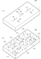
- This dielectric waveguide filter 101 is configured in a rectangular parallelepiped dielectric block 1.
- the dielectric block 1 is formed by processing dielectric ceramic, crystal, resin, or the like into a rectangular parallelepiped shape.
- Input / output pads 5A and 5B are formed on the bottom surface of the dielectric block 1.
- the dielectric block 1 is formed with input / output posts 4A, 4B protruding from the input / output pads 5A, 5B into the dielectric block 1.
- the dielectric block 1 is formed with through posts 2A to 2K penetrating from the upper surface to the lower surface.
- the dielectric block 1 is formed with a non-penetrating post 3U dug from the upper surface to a predetermined depth and a non-penetrating post 3L dug from the lower surface of the dielectric block 1 to a predetermined depth.
- a conductor film is formed on the inner surface of the outer surface of the dielectric block 1, each through post, and each non-through post.
- the periphery of the input / output pads 5A and 5B is separated from a conductor film used as a ground conductor.
- This conductive film is formed, for example, by metallizing an Ag electrode paste.
- the dielectric waveguide filter 101 includes four dielectric waveguide resonators 11A, 11B, 11C, and 11D.
- the dielectric waveguide resonator 11A is a first dielectric waveguide resonator according to the present invention
- the dielectric waveguide resonator 11B is a second dielectric waveguide resonator according to the present invention.
- the tube resonator 11C corresponds to a third dielectric waveguide resonator according to the present invention
- the dielectric waveguide resonator 11D corresponds to a fourth dielectric waveguide resonator according to the present invention.
- each of the resonators 11A, 11B, 11C, and 11D is a resonator having a TE101 mode as a fundamental mode.
- this is a resonance mode of an electromagnetic field distribution in which the magnetic field rotates in the plane direction along the XY plane with the Z direction as the electric field direction, and one electric field intensity peak in the X direction and one electric field intensity peak in the Y direction.
- a main coupling section MC12 is formed between the resonators 11A and 11B, a main coupling section MC23 is formed between the resonators 11B and 11C, and a main coupling section MC34 is formed between the resonators 11C and 11D.
- the sub-coupling portion SC14 is formed between the resonators 11A to 11D.
- the main joint MC12 shown in FIG. 3B is constituted by the through posts 2C, 2D and 2E shown in FIG. 3A.
- the main joint MC34 shown in FIG. 3B is constituted by the through posts 2C, 2J, and 2K shown in FIG.
- the sub-joining portion SC14 shown in FIG. 3B is constituted by the through posts 2A, 2B, and 2C shown in FIG.
- the main joint MC23 shown in FIG. 3B is constituted by the through posts 2F and 2G and the non-through posts 3U and 3L shown in FIG.
- the main coupling portion MC12 functions as an inductive coupling window for limiting the width (width in the Y direction) orthogonal to the electric field direction of the resonators 11A and 11B by the through posts 2C, 2D and 2E. They are inductively linked together.
- the main coupling portion MC34 acts as an inductive coupling window for limiting the width (width in the Y direction) orthogonal to the electric field direction of the resonators 11C and 11D by the through posts 2C, 2J and 2K. They are inductively linked together.
- the sub-coupling portion SC14 functions as an inductive coupling window for limiting the width (width in the X direction) orthogonal to the electric field direction of the resonators 11A and 11D by the through posts 2A, 2B and 2C. 11Ds are inductively linked.
- the gap between the non-penetrating post 3U and the non-penetrating post 3L is a capacitance that limits the width of the resonators 11B and 11C in the electric field direction (Z direction).
- the resonators 11B-11C are capacitively coupled to each other because they function as a capacitive coupling window.
- the through posts 2C, 2F, and 2G limit the width (width in the X direction) orthogonal to the electric field direction of the resonators 11B and 11C.
- the electric field direction (Z direction) by the non-through posts 3U and 3L is used.
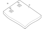
- FIG. 4 is a partial perspective view of a circuit board 90 on which the dielectric waveguide filter 101 is mounted.
- the ground conductor 10 and the input / output lands 15A and 15B are formed on the circuit board 90.
- the input / output pads 5A and 5B of the dielectric waveguide filter 101 are connected to the input / output lands 15A and 15B.
- the ground conductor formed on the bottom surface of the waveguide filter 101 is connected to the ground conductor 10 of the circuit board 90.
- the circuit board 90 is formed with transmission lines such as strip lines, microstrip lines, and coplanar lines, which are connected to the input / output lands 15A and 15B.
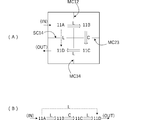
- FIGS. 5A and 5B are views showing a coupling structure of four resonators constituting the dielectric waveguide filter 101 of the present embodiment.
- the resonator 11A is a first-stage (first-stage) resonator
- the resonator 11B is a second-stage resonator
- the resonator 11C is a third-stage resonator.
- the resonator 11D is a fourth-stage (final-stage) resonator.
- a path indicated by a double line is a main connection path, and a broken line is a sub-connection path.
- “L” represents inductive coupling
- “C” represents capacitive coupling.
- the resonators 11A, 11B, 11C, and 11D are arranged along a main coupling path for signal propagation, and the main coupling section MC12 is an inductive coupling section.
- MC23 is a capacitive coupling part, and main coupling part MC34 is an inductive coupling part. That is, the main coupling portion is composed of the inductive coupling portion and the capacitive coupling portion, and the inductive coupling portion and the capacitive coupling portion are alternately and repeatedly arranged along the main coupling path.
- the main coupling portion between the resonator 11A for inputting / outputting a signal to the outside and the resonator 11B coupled to the resonator 11A is inductive. It is a joint.
- a main coupling portion between a resonator 11D to which signals are input and output to and from the outside and a resonator 11C coupled to the resonator 11D is an inductive coupling portion.
- the resonators 11A and 11D are arranged along the sub-coupling path in addition to the main coupling path. That is, the sub-coupling portion SC14 is formed between the resonator 11A and the resonator 11D.
- the sub coupling SC14 is an inductive coupling, and the coupling of the sub coupling SC14 is weaker than the coupling of the main couplings MC12, MC23 and MC34.
- the absolute value of the coupling coefficient of the sub coupling unit SC14 is It is smaller than the absolute value of the coupling coefficient of the coupling portions MC12, MC23, and MC34.
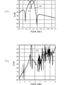
- FIG. 6 (A) and 6 (B) are diagrams showing the frequency characteristics of the reflection characteristics and the pass characteristics of the dielectric waveguide filter 101.
- FIG. FIG. 6B has a wider range of the frequency axis than FIG. 6A.
- the dielectric waveguide filter 101 of the present embodiment has a pass band at 3.3 GHz to 3.4 GHz, has a lower attenuation pole at 3.17 GHz, It has a high-frequency attenuation pole at 3.48 GHz.
- the transmission phase of the resonator is delayed by 90 ° at a frequency lower than the resonance frequency of the resonator, and advanced by 90 ° at a frequency higher than the resonance frequency. Since the phases of the inductive coupling and the capacitive coupling are inverted, when the inductive coupling and the capacitive coupling are combined, the signal transmitted through the main coupling path and the signal transmitted through the sub coupling path have opposite phases and the same amplitude. There are certain frequencies. An attenuation pole appears at this frequency.
- the first resonator 11A and the second resonator 11B are inductively coupled
- the second resonator 11B and the third resonator 11C are capacitively coupled
- the third resonator 11C and the fourth resonator 11D are inductively coupled with each other and jump over the second resonator 11B and the third resonator 11C
- the first resonator 11A and the fourth resonator 11D are sub-coupled.
- the phase in the main coupling path from the first resonator 11A to the fourth resonator 11D and the phase in the sub coupling path from the first resonator 11A to the fourth resonator 11D is inverted in the low band of the pass band, and is also inverted in the high band. That is, attenuation poles appear in both the low band and the high band of the pass band.
- FIGS. 7A and 7B are schematic diagrams of a resonance system including two adjacent resonators R1 and R2.
- FIG. 7A is a perspective view of the resonance system
- FIG. 7B is a front view thereof.
- electric field waves of each mode of TE101, TE102, and TE103 are shown in a superimposed manner.
- there are resonance modes related to the propagation mode TE10 such as TE101, TE102, TE103,.
- the TE101 mode has an in-phase relationship between the resonator R1 and the resonator R2
- the resonance mode TE102 has an anti-phase relationship between the resonator R1 and the resonator R2
- the TE103 mode has a phase relationship between the resonator R1 and the resonator R2.
- the coupling between the TE101 mode (in-phase) and the TE102 mode (out-of-phase) is defined as inductive coupling
- the coupling between the TE102 mode (out-of-phase) and the TE103 mode (in-phase) is induced. Since the coupling has a relationship in which the phase is inverted with respect to the sexual coupling, it is capacitive coupling.
- the capacitive coupling is a coupling between the TE102 mode, which is a higher-order mode, and the TE103 mode, which is a higher-order mode
- the TE101 mode which is a lower-order resonance mode as spurious
- the inductive coupling is a coupling between the TE101 mode, which is the fundamental mode, and the TE102 mode, so that no spurious is generated on the lower frequency side than the pass band (because there are no lower-order modes). Therefore, by arranging the capacitive coupling portion between the inductive coupling portions along the main coupling path, a low-order spurious response due to the capacitive coupling is suppressed.
- FIG. 8 is a transparent perspective view showing the structure of a capacitive coupling portion formed by simplifying the non-penetrating post 3 shown in FIG. 2B.
- the protrusion height (depth) of the non-penetrating post 3 from the lower surface of the dielectric block 1 is represented by D
- the width is represented by W
- the thickness is represented by T.
- W 6.6 mm
- T 1.0 mm.
- the height H of each resonator is 5.5 mm
- the width XW in the X direction is 13 mm
- the width YW in the Y direction is 13 mm.
- FIG. 9 is a diagram showing the characteristics of each resonance mode when the horizontal axis indicates the depth of the non-penetrating post 3 and the vertical axis indicates the resonance frequency.
- the frequency of the TE101 mode and the frequency of the TE103 mode decrease, but the TE102 mode is not affected. Since the frequency spacing of each mode corresponds to the strength of the coupling, the coupling can be adjusted by the depth of the non-penetrating post. Therefore, by setting the frequencies of the TE102 mode and the TE103 mode, which become capacitive coupling, to frequencies near the passband (3.5 GHz), capacitive coupling suitable for the filter characteristics of the target specification can be obtained.
- FIG. 8 shows the structure of the capacitive coupling portion formed by a single non-penetrating post obtained by simplifying the non-penetrating post 3 shown in FIG. 2B, but as shown in FIG. Similarly, when the non-penetrating posts are formed from the upper and lower surfaces of the dielectric block, the same characteristics as those shown in FIG. 9 can be obtained by the gap G between the two non-penetrating posts.
- FIG. 10A is an external perspective view of the dielectric waveguide filter 102 according to the second embodiment
- FIG. 10B is a transparent perspective view showing the internal structure of the dielectric waveguide filter 102. .
- This dielectric waveguide filter 102 is formed in a rectangular parallelepiped dielectric block 1.
- Input / output pads 5A and 5B are formed on the bottom surface of the dielectric block 1.
- the dielectric block 1 is formed with input / output posts 4A, 4B protruding from the input / output pads 5A, 5B into the dielectric block 1. Further, the dielectric block 1 is formed with through posts 2A, 2B, 2C, 2D, 2E, 2F penetrating from the upper surface to the lower surface.
- the dielectric block 1 has non-penetrating posts 3A, 3B, 3C dug from the lower surface to a predetermined depth. Further, the dielectric block 1 is formed with resonance frequency adjusting posts 6B, 6C, 6F, 6G dug from the lower surface to a predetermined depth.
- a conductor film is formed on the inner surface of the outer surface of the dielectric block 1, each through post, and each non-through post.
- the periphery of the input / output pads 5A and 5B is separated from a conductor film used as a ground conductor.
- the two-dot chain line is an imaginary line indicating the division of the resonator formed in the dielectric block 1.
- the dielectric waveguide filter 102 includes eight resonators 11A to 11H. Each of these resonators 11A to 11H is a resonator having a TE101 mode as a fundamental mode.
- the input / output pads 5A and 5B are circular.
- Each of the through posts 2A, 2B, 2C, 2D, 2E, 2F is a hole having an oval cross section, and forms a conductor wall having a predetermined width.
- the formation portions of these through posts 2A, 2B, 2C, 2D, 2E, 2F constitute an inductive coupling portion, and the formation portions of the non-through posts 3A, 3B, 3C constitute a capacitive coupling portion.
- the resonance frequency adjusting posts 6B, 6C, 6F, 6G are provided for finely adjusting the resonance frequencies of the resonators 11B, 11C, 11F, 11G. By determining the height (depth) of these resonance frequency adjusting posts 6B, 6C, 6F, 6G, the resonance frequencies of the resonators 11B, 11C, 11F, 11G are determined respectively.
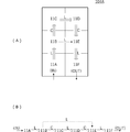
- FIGS. 11A and 11B are views showing a coupling structure of eight resonators constituting the dielectric waveguide filter 102 of the present embodiment.
- the resonator 11A is a first-stage (initial-stage) resonator
- the resonator 11H is an eighth-stage (final-stage) resonator.
- the resonators 11B, 11C, 11D, 11E, 11F and 11G of the second to seventh stages are arranged in order between the resonators 11A to 11H.
- the path indicated by a double line is a main connection path, and the broken line is a sub-connection path.
- L represents inductive coupling
- C represents capacitive coupling.
- the resonators 11A to 11H are arranged along the main coupling path for signal propagation, and the main coupling section is composed of an inductive coupling section and a capacitive coupling section.
- the inductive coupling part and the capacitive coupling part are alternately and repeatedly arranged along the main coupling path.
- the main coupling between the resonator 11A for inputting / outputting a signal to the outside and the resonator 11B coupled to the resonator 11A is inductive. It is a joint.
- a main coupling portion between a resonator 11H to which a signal is input and output to and from the outside and a resonator 11G coupled to the resonator 11H is an inductive coupling portion.
- the resonator 11A and the resonator 11D are sub-coupled (jump-coupled) at a sub-coupling portion that is an inductive coupling portion.
- the resonator 11C and the resonator 11F are sub-coupled (jump-coupled) at a sub-coupling portion that is an inductive coupling portion.
- the resonator 11E and the resonator 11H are sub-coupled (jump-coupled) at a sub-coupling portion that is an inductive coupling portion.
- the connection at each sub-connection is weaker than the connection at the main connection.
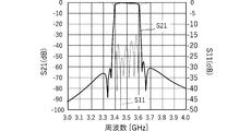
- FIG. 12 is a diagram showing the frequency characteristics of the reflection characteristics and the pass characteristics of the dielectric waveguide filter 102.
- S11 is a reflection characteristic
- S21 is a transmission characteristic.
- the dielectric waveguide filter 102 of the present embodiment has a pass band in the range of 3.4 GHz to 3.6 GHz, has lower attenuation poles in 3.34 GHz and 3.36 GHz, and has a higher attenuation pole in 3.63 GHz and 3.66 GHz. Of the attenuation pole.
- the resonators 11A to 11D correspond to the first to fourth resonators according to the present invention, respectively. Further, the resonators 11C to 11F also correspond to the first to fourth resonators according to the present invention, respectively. Further, the resonators 11E to 11H also correspond to the first to fourth resonators according to the present invention, respectively.
- the dielectric waveguide filter 102 of the present embodiment also has a capacitance among a plurality of coupling portions forming the main coupling portion and the sub coupling portion.
- the number of sexual junctions is less than the number of inductive junctions. Therefore, the spurious response appearing in a region lower than the pass band is suppressed without the low-order mode excitation caused by the capacitive coupling notably appearing.
- FIG. 13A is an external perspective view of a dielectric waveguide filter 103A according to the third embodiment
- FIG. 13B is a transparent perspective view showing the internal structure of the dielectric waveguide filter 103A. .
- the dielectric waveguide filter 103A is configured in a rectangular parallelepiped dielectric block 1.
- the dielectric block 1 has through posts 2AD, 2BE, and 2CF penetrating from the upper surface to the lower surface.
- the through post 2AD is obtained by connecting and integrating the through post 2A and the through post 2D provided in the dielectric waveguide filter 102 shown in FIG. 10B.
- the through post 2BE is formed by connecting the through post 2B and the through post 2E of the dielectric waveguide filter 102 shown in FIG.
- the through post 2CF is formed by connecting and integrating the through post 2C and the through post 2F provided in the dielectric waveguide filter 102 shown in FIG. 10B.
- Each of the through posts is T-shaped in plan view.
- the other components are the same as those of the dielectric waveguide filter 102 shown in the second embodiment.
- the inductive coupling portion of the main coupling portion and the inductive coupling portion of the sub coupling portion may be formed as an integrated post.
- FIG. 14A is an external perspective view of another dielectric waveguide filter 103B according to the third embodiment
- FIG. 14B is a transparent perspective view showing the internal structure of the dielectric waveguide filter 103B. It is.
- the dielectric waveguide filter 103B is configured in a rectangular parallelepiped dielectric block 1.
- the dielectric block 1 has through posts 2AD, 2BE, and 2CF penetrating from the upper surface to the lower surface.
- the through post 2AD connects the through post 2A and the through post 2D provided in the dielectric waveguide filter 102 shown in FIG. 10B.
- the through post 2BE is formed by connecting the through post 2B and the through post 2E of the dielectric waveguide filter 102 shown in FIG.
- the through post 2CF is formed by connecting and integrating the through post 2C and the through post 2F provided in the dielectric waveguide filter 102 shown in FIG. 10B.
- the through posts 2AD and 2CF are L-shaped in plan view, and the through posts 2BE are T-shaped in plan view.
- the other components are the same as those of the dielectric waveguide filter 102 shown in the second embodiment.
- the through posts constituting the inductive coupling portion are continuous over a plurality of coupling portions. May be.
- FIG. 15A is an external perspective view of still another dielectric waveguide filter 103C according to the third embodiment
- FIG. 15B is a perspective view showing the internal structure of the dielectric waveguide filter 103C.
- the dielectric waveguide filter 103C is configured in the rectangular parallelepiped dielectric block 1.
- the dielectric block 1 is formed with through posts 2A, 2BE, 2CF, 2D penetrating from the upper surface to the lower surface.
- the dielectric block 1 has non-penetrating posts 3A, 3B, 3C dug from the lower surface to a predetermined depth.
- the penetrating post 2A and the non-penetrating post 3A are connected and integrated.
- the through post 2BE and the non-through post 3B are connected and integrated.
- the through post 2CF is obtained by connecting and integrating the through post 2C and the through post 2F provided in the dielectric waveguide filter 102 shown in FIG. 10B.
- the through post forming the inductive coupling portion and the non-through post forming the capacitive coupling portion may be continuous. Further, as described above, the capacitive coupling portion of the main coupling portion and the inductive coupling portion of the sub coupling portion may be formed as an integrated post.
- the inductive coupling portion of the main coupling portion and the capacitive coupling portion of the sub-coupling portion may be formed as an integrated post.
- the capacitive coupling part of the main coupling part and the capacitive coupling part of the sub coupling part may be formed as an integrated post.
- the main joint and the sub joint are configured as an integral common post.
- the capacitive coupling part of the main coupling part may be constituted by an integrated post.
- the capacitive coupling part of the main coupling part and the capacitive coupling part of the main coupling part may be formed by an integrated post.
- ⁇ 4th Embodiment an example of a dielectric waveguide filter in which the structure of a jump coupling portion is different from that described above will be described.
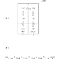
- FIGS. 16A and 16B are diagrams showing a coupling structure of six resonators constituting a dielectric waveguide filter 104A according to the fourth embodiment.
- the resonator 11A is a first-stage (initial-stage) resonator
- the resonator 11F is a sixth-stage (final-stage) resonator.
- the resonators 11B, 11C, 11D and 11E of the second to fifth stages are arranged in order between the resonators 11A to 11F.
- FIGS. 16A and 16B the path indicated by a double line is a main connection path, and the broken line is a sub-connection path.
- “L” represents inductive coupling
- “C” represents capacitive coupling.
- the resonators 11A to 11F are arranged along the main coupling path for signal propagation, and the main coupling section is composed of an inductive coupling section and a capacitive coupling section.
- the inductive coupling part and the capacitive coupling part are alternately and repeatedly arranged along the main coupling path.
- the resonator 11B and the resonator 11E are sub-coupled (jump-coupled) at a sub-coupling portion that is an inductive coupling portion.
- the two resonators coupled by the sub-coupling are coupled in the main coupling path in the order of inductive coupling ⁇ capacitive coupling ⁇ inductive coupling.
- the resonator 11B and the resonator 11E coupled by the sub-coupling are capacitively coupled to inductive in the main coupling path. Coupling is coupled in the order of capacitive coupling.
- the resonator 11B and the resonator 11E are inductively coupled in the sub-coupling path.
- two resonators coupled in the order of capacitive coupling ⁇ inductive coupling ⁇ capacitive coupling on the main coupling path may be sub-coupled.
- FIGS. 17A and 17B are diagrams showing a coupling structure of six resonators constituting another dielectric waveguide filter 104B according to the fourth embodiment.
- the resonator 11A is a first-stage (initial-stage) resonator
- the resonator 11F is a sixth-stage (final-stage) resonator.
- the resonators 11B, 11C, 11D and 11E of the second to fifth stages are arranged in order between the resonators 11A to 11F.
- FIGS. 17A and 17B The paths indicated by double lines in FIGS. 17A and 17B are main connection paths. 17A and 17B, “L” indicates inductive coupling, and “C” indicates capacitive coupling. This dielectric waveguide filter 104B has no sub-coupling path. That is, there is no jump connection.
- the resonators 11A to 11F are arranged along the main coupling path for signal propagation, and the main coupling section is composed of an inductive coupling section and a capacitive coupling section.
- the inductive coupling part and the capacitive coupling part are alternately and repeatedly arranged along the main coupling path.
- the resonator at the input / output stage and the resonator main-coupled thereto are inductively coupled.
- the first stage is used.
- the (first-stage) resonator 11A and the second-stage resonator 11B are capacitively coupled, and the sixth-stage (final-stage) resonator 11F and the fifth-stage resonator 11E are capacitively coupled. .
- the second-stage resonator 11B and the fifth-stage resonator 11E are capacitive and not sub-coupled (jump-coupled). This is because when capacitive coupling is performed, three stages of capacitive coupling continue in the path of the resonators 11A, 11B, 11E, and 11F.
- a resonator for inputting / outputting a signal to / from the outside and a coupling to the resonator are provided.
- the main coupling between the resonator and the active resonator is an inductive coupling.
- the capacitive coupling is continuous in three stages. There is no. Therefore, the attenuation pole can be easily formed by providing the sub-coupling portion.
- a structure in which the resonator in the input / output stage and the resonator that is main-coupled thereto may be capacitively coupled may be used.
- FIG. 18A is an external perspective view of the dielectric waveguide filter 105 according to the fifth embodiment
- FIG. 18B is a transparent perspective view showing the internal structure of the dielectric waveguide filter 105. .
- This dielectric waveguide filter 105 is not formed in a rectangular parallelepiped dielectric block, but is formed in a part of the substrate 9.
- the substrate 9 includes a dielectric plate (insulator plate), a conductor film 7 formed on an upper surface thereof, and a conductor film 8 formed on a lower surface thereof.
- This substrate 9 is, for example, a glass epoxy (FR-4) substrate.
- a plurality of through posts (via conductors) 2V are arranged at positions corresponding to the outer surface of the dielectric block 1 shown in FIG.
- Conductive films are formed on the inner surfaces of the through posts 2V, and the conductive films are electrically connected to the conductive films 7 and 8. With this structure, a wall surface equivalent to the outer surface of the dielectric block 1 is formed.
- FIGS. 18A and 18B the internal structure surrounded by the through post 2V is the same as that shown in FIGS. 1A and 1B.
- a dielectric waveguide filter may be constituted by a substrate integrated waveguide (SIW: Substrate Integrated Waveguide) or a post-wall waveguide (PWW: Post-Wall Waveguide).
- SIW substrate integrated waveguide
- PWW Post-wall waveguide
- the adjacent spacing of the through posts 2V constituting the equivalent wall surface is such that the cut-off frequency of the arranged through posts 2V is higher than the pass band of the filter.
- the adjacent interval between the through posts 2V may be determined as shown below.
- fc cut-off frequency a: distance between holes of through post 2V b: distance between upper and lower conductor films 7-8
- Co speed of light in vacuum
- ⁇ r relative permittivity of dielectric part (insulator part) of substrate m
- n orders of the waveguide mode.
- the cutoff frequency is a measure of the ease of passing electromagnetic waves (waveguide mode: TE mode), and electromagnetic waves with frequencies below the cutoff frequency are cut off and do not pass. If the electromagnetic wave leaks from the interval between the arranged through posts 2V, the loss increases. Therefore, it is important to narrow the interval between the through posts 2V and make the cutoff frequency higher than the pass band of the filter.
- the cutoff frequency fc is at least higher than the center frequency f of the filter, the loss will increase.
- the cutoff frequency must be increased accordingly, and the distance between the holes of the through post 2V needs to be reduced.
- the inner surface of the through post 2V may have a solid structure filled with a conductor.
- the cross-sectional shape of the through post 2V may not be circular, but may be oval or rounded rectangle.
- the input / output structure is not limited to the lower surface or the upper surface of the substrate 9, and may be provided on an equivalent side wall constituted by a plurality of through posts 2V.
- FIG. 19 is a block diagram of a mobile phone base station.
- the circuit of the mobile phone base station includes an FPGA 121, a DA converter 122, band-pass filters 123, 126, 131, a single mixer 125, a local oscillator 124, an attenuator 127, an amplifier 128, a power amplifier 129, a detector 130, and an antenna 132.
- FPGA 121 FPGA 121
- DA converter 122 band-pass filters 123, 126, 131
- band-pass filters 123, 126, 131 a single mixer 125
- a local oscillator 124 an attenuator 127
- an amplifier 128, a power amplifier 129 a detector 130
- an antenna 132 an antenna 132.
- the FPGA 121 generates a modulated digital signal.
- the DA converter 122 converts the modulated digital signal into an analog signal.
- the band-pass filter 123 passes signals in the baseband frequency band and removes signals in other frequency bands.
- the single mixer 125 mixes the output signal of the band-pass filter 123 and the oscillation signal of the local oscillator 124 and performs up-conversion.
- the band-pass filter 126 removes unnecessary frequency bands generated by the up-conversion.
- the attenuator 127 adjusts the intensity of the transmission wave, and the amplifier 128 amplifies the transmission wave in the preceding stage.
- the power amplifier 129 power-amplifies the transmission wave, and transmits the transmission wave from the antenna 132 via the band-pass filter 131.
- the band-pass filter 131 passes a transmission wave in a transmission frequency band.
- Detector 130 detects transmission power.
- the dielectric waveguide filters shown in the first to fourth embodiments can be used as the band-pass filters 126 and 131 that pass the frequency band of the transmission wave. .
- G gaps MC12, MC23, MC34: main coupling portions R1, R2: dielectric waveguide resonator SC14: sub coupling portion 1: dielectric blocks 2A, 2B, 2C, 2D, 2E, 2F, 2G, 2J, 2K , 2V: through post 2AD, 2BE, 2CF: through post 3, 3A, 3B, 3C, 3L, 3U: non-through post 4A, 4B, 5A, 5B: input / output pads 6B, 6C, 6F, 6G: resonance frequency Adjustment posts 7, 8 Conductive film 9 Substrate 10 Ground conductors 11A, 11B, 11C, 11D, 11E, 11F, 11G, 11H Dielectric waveguide resonators 15A, 15B Input / output lands 90 Circuit Substrates 101, 102, 103A, 103B, 103C, 104A, 104B, 105: dielectric waveguide filter 121: FPGA 122 ...
Landscapes
- Control Of Motors That Do Not Use Commutators (AREA)
Abstract
Un filtre de guide d'ondes diélectrique (101) comprend : quatre résonateurs de guide d'ondes diélectriques ou plus qui sont agencés le long d'un trajet de couplage principal pour la propagation de signaux ; et une pluralité de parties de couplage principal qui sont chacune disposées entre des résonateurs de guide d'ondes diélectriques adjacents le long du trajet de couplage principal, parmi les résonateurs de guide d'ondes diélectriques. Les parties de couplage principal comprennent des parties de couplage inductif et des parties de couplage capacitif, qui sont agencées de façon alternée et répétée le long du trajet de couplage principal. Grâce à cette configuration, avec un plus petit nombre d'étages de résonateur, les caractéristiques d'atténuation sont réglées de manière abrupte dans une plage à partir d'une bande passante et les réponses plus élevées et parasites apparaissant dans une plage inférieure à la bande passante sont supprimées.
Priority Applications (3)
| Application Number | Priority Date | Filing Date | Title |
|---|---|---|---|
| CN201980044568.4A CN112385078B (zh) | 2018-07-02 | 2019-05-22 | 电介质波导管滤波器 |
| JP2020528712A JP6927434B2 (ja) | 2018-07-02 | 2019-05-22 | 誘電体導波管フィルタ |
| US17/110,386 US11362406B2 (en) | 2018-07-02 | 2020-12-03 | Dielectric waveguide filter |
Applications Claiming Priority (2)
| Application Number | Priority Date | Filing Date | Title |
|---|---|---|---|
| JP2018125911 | 2018-07-02 | ||
| JP2018-125911 | 2018-07-02 |
Related Child Applications (1)
| Application Number | Title | Priority Date | Filing Date |
|---|---|---|---|
| US17/110,386 Continuation US11362406B2 (en) | 2018-07-02 | 2020-12-03 | Dielectric waveguide filter |
Publications (1)
| Publication Number | Publication Date |
|---|---|
| WO2020008748A1 true WO2020008748A1 (fr) | 2020-01-09 |
Family
ID=69060874
Family Applications (1)
| Application Number | Title | Priority Date | Filing Date |
|---|---|---|---|
| PCT/JP2019/020291 Ceased WO2020008748A1 (fr) | 2018-07-02 | 2019-05-22 | Filtre de guide d'ondes diélectrique |
Country Status (4)
| Country | Link |
|---|---|
| US (1) | US11362406B2 (fr) |
| JP (1) | JP6927434B2 (fr) |
| CN (1) | CN112385078B (fr) |
| WO (1) | WO2020008748A1 (fr) |
Cited By (3)
| Publication number | Priority date | Publication date | Assignee | Title |
|---|---|---|---|---|
| TWI748732B (zh) * | 2020-08-20 | 2021-12-01 | 大陸商廈門松元電子有限公司 | 具有電容耦合金屬圖案的混合異波長諧振帶通濾波器 |
| CN115668633A (zh) * | 2020-07-22 | 2023-01-31 | 株式会社村田制作所 | 带通滤波器以及具备该带通滤波器的高频前端电路 |
| WO2025238881A1 (fr) * | 2024-05-15 | 2025-11-20 | 三菱電機株式会社 | Structure d'atténuation d'ondes électromagnétiques |
Families Citing this family (3)
| Publication number | Priority date | Publication date | Assignee | Title |
|---|---|---|---|---|
| EP3972047A4 (fr) * | 2019-05-14 | 2022-12-21 | Rosenberger Technologies Co., Ltd. | Filtre à couplage transversal |
| US20230042666A1 (en) * | 2021-08-09 | 2023-02-09 | Meta Platforms, Inc. | Apparatus, system, and method for achieving improved ground station design |
| CN116031602B (zh) * | 2021-10-26 | 2026-06-26 | 深圳三星通信技术研究有限公司 | 一种介质波导谐振器和多模介质波导谐振器 |
Citations (5)
| Publication number | Priority date | Publication date | Assignee | Title |
|---|---|---|---|---|
| JPS50104547A (fr) * | 1974-01-18 | 1975-08-18 | ||
| JPS6324704A (ja) * | 1986-07-17 | 1988-02-02 | Fujitsu Ltd | 帯域通過型濾波器 |
| US20090231064A1 (en) * | 2006-08-04 | 2009-09-17 | Dielectric Laboratories, Inc. | Wideband dielectric waveguide filter |
| WO2016191116A1 (fr) * | 2015-05-22 | 2016-12-01 | Cts Corporation | Filtre en guide d'ondes diélectrique à couplage direct et à autre couplage croisé |
| WO2018139321A1 (fr) * | 2017-01-27 | 2018-08-02 | 株式会社村田製作所 | Filtre de guide d'ondes diélectrique, circuit frontal haute fréquence et dispositif de communication |
Family Cites Families (11)
| Publication number | Priority date | Publication date | Assignee | Title |
|---|---|---|---|---|
| JP2001181029A (ja) * | 1999-10-12 | 2001-07-03 | Murata Mfg Co Ltd | 高周波用誘電体磁器組成物、誘電体共振器、誘電体フィルタ、誘電体デュプレクサおよび通信機装置 |
| US8823470B2 (en) * | 2010-05-17 | 2014-09-02 | Cts Corporation | Dielectric waveguide filter with structure and method for adjusting bandwidth |
| KR20120003354A (ko) * | 2010-07-02 | 2012-01-10 | 한국전자통신연구원 | 이중 모드 공진기 및 삼중 모드 공진기를 포함하는 공진기 필터 및 다이플렉서 |
| JP5688977B2 (ja) * | 2011-01-13 | 2015-03-25 | 東光株式会社 | 誘電体導波管の入出力接続構造 |
| JP5675449B2 (ja) | 2011-03-11 | 2015-02-25 | 東光株式会社 | 誘電体導波管フィルタ |
| US9030279B2 (en) | 2011-05-09 | 2015-05-12 | Cts Corporation | Dielectric waveguide filter with direct coupling and alternative cross-coupling |
| US9130255B2 (en) | 2011-05-09 | 2015-09-08 | Cts Corporation | Dielectric waveguide filter with direct coupling and alternative cross-coupling |
| US9130258B2 (en) * | 2013-09-23 | 2015-09-08 | Cts Corporation | Dielectric waveguide filter with direct coupling and alternative cross-coupling |
| WO2018012294A1 (fr) | 2016-07-13 | 2018-01-18 | 株式会社村田製作所 | Circuit de filtre de guide d'ondes, substrat de montage pour des filtres de guide d'ondes et filtre de guide d'ondes |
| WO2018029956A1 (fr) * | 2016-08-10 | 2018-02-15 | 株式会社村田製作所 | Filtre à guide d'ondes diélectrique, circuit frontal haute fréquence, système mimo massif et procédé de fabrication d'un filtre à guide d'ondes diélectrique |
| CN106960994A (zh) * | 2017-04-25 | 2017-07-18 | 四川省韬光通信有限公司 | 一种便于调节频率与耦合带宽的介质滤波器 |
-
2019
- 2019-05-22 WO PCT/JP2019/020291 patent/WO2020008748A1/fr not_active Ceased
- 2019-05-22 CN CN201980044568.4A patent/CN112385078B/zh active Active
- 2019-05-22 JP JP2020528712A patent/JP6927434B2/ja active Active
-
2020
- 2020-12-03 US US17/110,386 patent/US11362406B2/en active Active
Patent Citations (5)
| Publication number | Priority date | Publication date | Assignee | Title |
|---|---|---|---|---|
| JPS50104547A (fr) * | 1974-01-18 | 1975-08-18 | ||
| JPS6324704A (ja) * | 1986-07-17 | 1988-02-02 | Fujitsu Ltd | 帯域通過型濾波器 |
| US20090231064A1 (en) * | 2006-08-04 | 2009-09-17 | Dielectric Laboratories, Inc. | Wideband dielectric waveguide filter |
| WO2016191116A1 (fr) * | 2015-05-22 | 2016-12-01 | Cts Corporation | Filtre en guide d'ondes diélectrique à couplage direct et à autre couplage croisé |
| WO2018139321A1 (fr) * | 2017-01-27 | 2018-08-02 | 株式会社村田製作所 | Filtre de guide d'ondes diélectrique, circuit frontal haute fréquence et dispositif de communication |
Cited By (4)
| Publication number | Priority date | Publication date | Assignee | Title |
|---|---|---|---|---|
| CN115668633A (zh) * | 2020-07-22 | 2023-01-31 | 株式会社村田制作所 | 带通滤波器以及具备该带通滤波器的高频前端电路 |
| TWI748732B (zh) * | 2020-08-20 | 2021-12-01 | 大陸商廈門松元電子有限公司 | 具有電容耦合金屬圖案的混合異波長諧振帶通濾波器 |
| WO2025238881A1 (fr) * | 2024-05-15 | 2025-11-20 | 三菱電機株式会社 | Structure d'atténuation d'ondes électromagnétiques |
| JPWO2025238881A1 (fr) * | 2024-05-15 | 2025-11-20 |
Also Published As
| Publication number | Publication date |
|---|---|
| CN112385078B (zh) | 2022-03-01 |
| US11362406B2 (en) | 2022-06-14 |
| JPWO2020008748A1 (ja) | 2021-06-24 |
| JP6927434B2 (ja) | 2021-09-01 |
| CN112385078A (zh) | 2021-02-19 |
| US20210091441A1 (en) | 2021-03-25 |
Similar Documents
| Publication | Publication Date | Title |
|---|---|---|
| CN112385078B (zh) | 电介质波导管滤波器 | |
| KR100418607B1 (ko) | 대역필터, 듀플렉서, 고주파 모듈 및 통신장치 | |
| KR100338590B1 (ko) | 유전체 필터, 유전체 듀플렉서 및 통신 장치 | |
| CN115425375B (zh) | 一种带通滤波器及其小型化cq拓扑结构 | |
| JP3498649B2 (ja) | 誘電体フィルタ、デュプレクサおよび通信装置 | |
| WO2022209278A1 (fr) | Filtre diélectrique | |
| US11742557B2 (en) | Dielectric waveguide filter | |
| US12107312B2 (en) | Band pass filter and high frequency front-end circuit including same | |
| JP4565145B2 (ja) | 超広帯域バンドパスフィルタ | |
| JP2001203503A (ja) | ストリップ線路フィルタ、デュプレクサ、フィルタ装置、通信装置およびストリップ線路フィルタの特性調整方法 | |
| CN1329763A (zh) | 微带滤波器装置 | |
| US20240136995A1 (en) | Filter device and radio frequency front end circuit | |
| KR100449226B1 (ko) | 유전체 듀플렉서 | |
| US12206149B2 (en) | Dielectric waveguide resonator and filter including at least one internal conductor physically isolated from first and second surface conductors and overlapping therewith | |
| KR100369211B1 (ko) | 일체형 유전체 듀플렉서 | |
| KR100524545B1 (ko) | 유전체 필터, 유전체 듀플렉서 및 통신장치 | |
| JP4327876B2 (ja) | 分割給電結合リング共振器対楕円関数フィルタのための装置及び方法 | |
| JP4438253B2 (ja) | バンドパスフィルタの特性調整方法 | |
| JP2000252705A (ja) | 帯域通過フィルタおよびそれを用いたデュプレクサおよびそれらを用いた高周波モジュールおよびそれを用いた通信装置 | |
| KR100363787B1 (ko) | 일체형 유전체 듀플렉서 필터 | |
| SU843039A1 (ru) | Полосовой фильтр на запредельномВОлНОВОдЕ | |
| JP2002325002A (ja) | 高周波用共振部品及びそのスプリアス抑制方法並びにデュプレクサ及び無線通信装置 | |
| KR19990030747A (ko) | 마이크로 스트립 대역 통과 필터 | |
| JP2000077907A (ja) | 誘電体フィルタ | |
| JPH0758521A (ja) | ストリップライン共振器 |
Legal Events
| Date | Code | Title | Description |
|---|---|---|---|
| 121 | Ep: the epo has been informed by wipo that ep was designated in this application |
Ref document number: 19830384 Country of ref document: EP Kind code of ref document: A1 |
|
| ENP | Entry into the national phase |
Ref document number: 2020528712 Country of ref document: JP Kind code of ref document: A |
|
| NENP | Non-entry into the national phase |
Ref country code: DE |
|
| 122 | Ep: pct application non-entry in european phase |
Ref document number: 19830384 Country of ref document: EP Kind code of ref document: A1 |