WO2020008882A1 - Procédé de production de substrat transféré par couche de dispositif et substrat transféré par couche de dispositif - Google Patents
Procédé de production de substrat transféré par couche de dispositif et substrat transféré par couche de dispositif Download PDFInfo
- Publication number
- WO2020008882A1 WO2020008882A1 PCT/JP2019/024300 JP2019024300W WO2020008882A1 WO 2020008882 A1 WO2020008882 A1 WO 2020008882A1 JP 2019024300 W JP2019024300 W JP 2019024300W WO 2020008882 A1 WO2020008882 A1 WO 2020008882A1
- Authority
- WO
- WIPO (PCT)
- Prior art keywords
- layer
- substrate
- adhesive
- wafer
- transparent substrate
- Prior art date
- Legal status (The legal status is an assumption and is not a legal conclusion. Google has not performed a legal analysis and makes no representation as to the accuracy of the status listed.)
- Ceased
Links
Images
Classifications
-
- C—CHEMISTRY; METALLURGY
- C09—DYES; PAINTS; POLISHES; NATURAL RESINS; ADHESIVES; COMPOSITIONS NOT OTHERWISE PROVIDED FOR; APPLICATIONS OF MATERIALS NOT OTHERWISE PROVIDED FOR
- C09J—ADHESIVES; NON-MECHANICAL ASPECTS OF ADHESIVE PROCESSES IN GENERAL; ADHESIVE PROCESSES NOT PROVIDED FOR ELSEWHERE; USE OF MATERIALS AS ADHESIVES
- C09J183/00—Adhesives based on macromolecular compounds obtained by reactions forming in the main chain of the macromolecule a linkage containing silicon, with or without sulfur, nitrogen, oxygen, or carbon only; Adhesives based on derivatives of such polymers
- C09J183/04—Polysiloxanes
-
- G—PHYSICS
- G02—OPTICS
- G02F—OPTICAL DEVICES OR ARRANGEMENTS FOR THE CONTROL OF LIGHT BY MODIFICATION OF THE OPTICAL PROPERTIES OF THE MEDIA OF THE ELEMENTS INVOLVED THEREIN; NON-LINEAR OPTICS; FREQUENCY-CHANGING OF LIGHT; OPTICAL LOGIC ELEMENTS; OPTICAL ANALOGUE/DIGITAL CONVERTERS
- G02F1/00—Devices or arrangements for the control of the intensity, colour, phase, polarisation or direction of light arriving from an independent light source, e.g. switching, gating or modulating; Non-linear optics
- G02F1/01—Devices or arrangements for the control of the intensity, colour, phase, polarisation or direction of light arriving from an independent light source, e.g. switching, gating or modulating; Non-linear optics for the control of the intensity, phase, polarisation or colour
- G02F1/13—Devices or arrangements for the control of the intensity, colour, phase, polarisation or direction of light arriving from an independent light source, e.g. switching, gating or modulating; Non-linear optics for the control of the intensity, phase, polarisation or colour based on liquid crystals, e.g. single liquid crystal display cells
-
- G—PHYSICS
- G09—EDUCATION; CRYPTOGRAPHY; DISPLAY; ADVERTISING; SEALS
- G09F—DISPLAYING; ADVERTISING; SIGNS; LABELS OR NAME-PLATES; SEALS
- G09F9/00—Indicating arrangements for variable information in which the information is built-up on a support by selection or combination of individual elements
-
- H—ELECTRICITY
- H10—SEMICONDUCTOR DEVICES; ELECTRIC SOLID-STATE DEVICES NOT OTHERWISE PROVIDED FOR
- H10D—INORGANIC ELECTRIC SEMICONDUCTOR DEVICES
- H10D86/00—Integrated devices formed in or on insulating or conducting substrates, e.g. formed in silicon-on-insulator [SOI] substrates or on stainless steel or glass substrates
-
- H—ELECTRICITY
- H10—SEMICONDUCTOR DEVICES; ELECTRIC SOLID-STATE DEVICES NOT OTHERWISE PROVIDED FOR
- H10P—GENERIC PROCESSES OR APPARATUS FOR THE MANUFACTURE OR TREATMENT OF DEVICES COVERED BY CLASS H10
- H10P50/00—Etching of wafers, substrates or parts of devices
-
- H—ELECTRICITY
- H10—SEMICONDUCTOR DEVICES; ELECTRIC SOLID-STATE DEVICES NOT OTHERWISE PROVIDED FOR
- H10P—GENERIC PROCESSES OR APPARATUS FOR THE MANUFACTURE OR TREATMENT OF DEVICES COVERED BY CLASS H10
- H10P52/00—Grinding, lapping or polishing of wafers, substrates or parts of devices
-
- H—ELECTRICITY
- H10—SEMICONDUCTOR DEVICES; ELECTRIC SOLID-STATE DEVICES NOT OTHERWISE PROVIDED FOR
- H10P—GENERIC PROCESSES OR APPARATUS FOR THE MANUFACTURE OR TREATMENT OF DEVICES COVERED BY CLASS H10
- H10P95/00—Generic processes or apparatus for manufacture or treatments not covered by the other groups of this subclass
Definitions
- the present invention relates to a method for manufacturing an LCOS substrate in which a single-crystal silicon circuit is formed on a transparent substrate on one of two substrates sandwiching a liquid crystal layer, as a liquid crystal device, and to the substrate.
- a liquid crystal device using a single crystal silicon substrate as one of two substrates sandwiching a liquid crystal layer has been proposed. That is, a liquid crystal device in which a liquid crystal layer is sealed between a single crystal silicon substrate (element substrate) on which a transistor is formed and a glass substrate (counter substrate).
- LCOS a reflection type liquid crystal device using an opaque SOI (Silicon on Insulator) substrate and a transmission type liquid crystal device using a transparent SOI substrate have been proposed.
- Patent Document 1 A configuration example of a reflection type liquid crystal device is disclosed in Patent Document 1
- a configuration example of a transmission type liquid crystal device is disclosed in Patent Document 2.
- the reflection type configuration it is necessary to provide optical components such as a reflection mirror and a polarizing beam splitter outside the panel sandwiching the liquid crystal layer, and the transmission type liquid crystal device is advantageous in reducing the size and weight of the liquid crystal device. It is.
- the element substrate is required to have light transmissivity. Therefore, as exemplified in Patent Document 2, as an element substrate, an SOI substrate whose base material is transparent to visible light, for example, an SOS (Silicon on Sapphire) substrate, an SOQ (Silicon on Quartz) substrate, and an SOG (Silicon on Glass) A substrate or the like is used.
- a substrate in which silicon is a single crystal is preferable because the mobility of the element is high and the response of the liquid crystal device can be increased.
- a transistor including a pixel electrode is formed in a silicon layer, a liquid crystal layer is sandwiched between the transistor and a counter substrate to manufacture a transmissive LCOS panel.
- the substrate is transparent and an insulator, there is a problem that a quartz substrate does not correspond to a presence sensor or an electrostatic chuck of a silicon device manufacturing apparatus. Special processing corresponding to is required. Further, since a glass substrate other than quartz has a low glass transition temperature, it is difficult to manufacture a transistor. Furthermore, taking the SOS as an example, the size of the substrate is 150 mm, so that there is a problem that the cost is high. In order to reduce the cost, the size of the sapphire substrate may be increased to, for example, 200 mm or 300 mm. However, since sapphire substrates of these sizes are not generally distributed, there is a problem that the cost does not decrease significantly.
- Patent Document 3 a method of forming an element layer on an SOI substrate using silicon as a substrate and transferring the element layer to a transparent substrate. That is, an element is formed on an SOI substrate, temporarily bonded to another substrate using an adhesive, the back surface of the SOI is removed to form a chip, the obtained chip is aligned with a transparent substrate to be finally mounted, and then bonded and bonded. It is stated that the used substrate and adhesive are removed. It is described that glass is used as a substrate used for the temporary bonding, and the removal is performed by HF etching, and the adhesive is removed by chemical etching or plasma etching.
- the present invention has been made in view of the above circumstances, and relates to a method of transferring a device layer, particularly a device layer including a pixel electrode and a wiring layer for a microdisplay, onto a transparent substrate, and manufacturing a device layer transfer substrate. It is another object of the present invention to provide a transfer method and a substrate which can be carried out at a wafer level without being formed into chips, have a good yield, and can be easily carried out with a large diameter.
- the present invention is a method of manufacturing a device layer transfer substrate, Temporarily bonding the device layer side of the SOI wafer including the silicon layer, the insulator layer, and the device layer to a support substrate using a temporary bonding adhesive; Removing the silicon layer of the SOI wafer until the insulator layer is exposed to obtain a thinned device wafer; Applying a transfer adhesive to at least one of the exposed insulator layer or the transparent substrate of the thinned device wafer, Bonding the exposed insulator layer and the transparent substrate of the thinned device wafer via the transfer adhesive; And removing the support substrate in a state where the thinned device wafer, the transparent substrate, and the joined body are warped.
- a device layer transfer substrate wherein an insulator layer derived from an SOI wafer and a device layer are laminated in this order on a transparent substrate via a low stress adhesive.
- the device layer transfer substrate wherein the thickness of the insulator layer is 50 to 500 nm, and the thickness of the adhesive layer is 0.1 to 5 ⁇ m.
- a device layer formed on an SOI wafer can be transferred to a transparent substrate at a wafer level without being formed into chips.
- Such a method allows transfer without inverting the device layer.
- wiring for controlling the transparent conductor such as ITO for controlling the liquid crystal is taken, so that it is necessary to perform a via process after the transfer and a process of embedding with a conductive material.
- the present invention if a pad connected to the transparent conductor is formed on the uppermost layer, the above-described wiring processing is not required, and the process can be simplified.
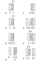
- FIG. 1 is a view conceptually showing a method for manufacturing a device layer transfer substrate according to the present invention.
- an object is to apply to a transmission type LCOS, and in order to obtain a light transmittance with visible light, an Si layer below an embedded oxide film which is an insulator layer is formed by an appropriate method which does not leave a processing mark. It is an object of the present invention to clarify an appropriate transfer method that enables processing without completely removing and thinning a device from wrinkles and peeling from an outer peripheral portion.
- the present invention relates to a method for manufacturing a device layer transfer substrate.
- the manufacturing method includes the following steps (i) to (v). (I) temporarily bonding the device layer side of the SOI wafer including a silicon layer, an insulator layer, and a device layer to a support substrate using a temporary bonding adhesive; (Ii) removing the silicon layer of the SOI wafer until the insulator layer is exposed to obtain a thinned device wafer; (Iii) applying a transfer adhesive to at least one of the exposed insulator layer or the transparent substrate of the thinned device wafer; (Iv) bonding the exposed insulator layer of the thinned device wafer and the transparent substrate via the transfer adhesive; (V) a step of removing the support substrate in a state where the thinned device wafer, the transparent substrate, and the joined body have warpage corrected.
- the device layer transfer substrate is a substrate in which an insulator layer and a device layer manufactured as an SOI (Silicon on Insulator) wafer are bonded to a transparent substrate, and a device layer is provided between the insulator layer and the transparent substrate. It refers to a substrate bonded via an adhesive layer. Therefore, the device layer transfer substrate is a substrate in which a transparent substrate, an adhesive layer, an insulator layer, and a device layer are laminated in this order.
- FIG. 1 is a diagram schematically illustrating a manufacturing method according to the present invention.
- the SOI wafer 14 is a substrate on which a silicon layer 11, an insulator layer 12, and a device layer 13 are stacked in this order.
- the silicon layer 11 is a layer of silicon (Si), and its thickness may be generally about 200 to 1000 ⁇ m, for example, about 750 to 800 ⁇ m for a 300 mm wafer, and about 700 to 750 ⁇ m for a 200 mm wafer.
- the insulator layer 12 is a layer of a buried oxide film (SiO 2 ), and its thickness may be generally about 50 to 500 nm.
- the device layer 13 is a layer in which a pixel electrode and a wiring layer for a micro display are formed on a single crystal silicon (Si) active layer.
- the thickness of the device layer 13 may be usually 2 ⁇ m to 10 ⁇ m, preferably about 4 ⁇ m to 6 ⁇ m, although it depends on the number of wirings.
- an electrode pad for controlling the liquid crystal optionally may be formed on the surface of the device layer 13.
- Such an SOI wafer 14 may be manufactured by an arbitrary method.
- the support substrate 15 used in the temporary bonding step depends on the method of curing the temporary bonding adhesive 16 to be used, but is preferably a substrate having a linear expansion coefficient similar to that of Si.
- a heat-resistant borosilicate glass such as Si wafer, Tempax (registered trademark), or a heat-resistant non-alkali glass such as EAGLE-XG (registered trademark) can be used. Not done.
- a UV-curable acrylic adhesive or an adhesive mainly composed of thermosetting modified silicone can be used.
- WSS manufactured by 3M
- TA1070T, TA2570V3, and TA4070 manufactured by Shin-Etsu Chemical Co., Ltd. can be laminated and used in this order.
- the layers are stacked so that the TA 4070T contacts the support substrate 15 and the TA 1070 contacts the device layer 13.
- the laminated structure of the temporary bonding adhesive 16 may be described as TA1070T / TA2570V3 / TA4070.
- thermosetting modified silicone as a main component
- the adhesive containing thermosetting modified silicone as a main component is excellent in acid resistance and alkali resistance when etching the back surface (silicon layer 11) in the step of obtaining a thinned device wafer following this step.
- the back surface refers to the back surface when the device layer is the front surface.
- the temporary bonding adhesive 16 is applied to the surface of the SOI wafer 14 on which the device layer 13 is formed and / or one main surface of the support substrate 15 by spin coating to a thickness of about 5 to 100 ⁇ m.
- temporary bonding is performed by, for example, UV irradiation or heating.
- the thickness of the temporary bonding adhesive 16 refers to the thickness after curing.
- the adhesive 16 for the temporary bonding is used to separately select an adhesive for protecting the device layer 13, an adhesive for forming a layer to be a release surface, and an adhesive for forming an adhesive layer with the support substrate 15, respectively. They can be used by lamination.
- the laminate obtained by bonding the SOI wafer 14 and the support substrate 15 obtained in this step with the temporary bonding adhesive 16 is also referred to as a temporary bonded body in this specification.
- Step of Obtaining a Thinned Device Wafer a step of obtaining a thinned device wafer is performed.
- the silicon layer 11 of the temporary bonded body is ground and thinned, and the trimmed silicon layer 11, the insulator layer 12, the device layer 13, and the temporary bonding adhesive 16 are edge-trimmed.
- a step of removing the silicon layer 11 remaining after the grinding and thinning step by etching with an acid is performed.
- FIG. 1B is a view conceptually showing a temporary bonded body of the support substrate 15 and the SOI wafer 14 after the silicon layer 11 has been thinly processed.
- the silicon layer 11 can be thinned by processing using a combination of grinding wheels # 600 to # 2000. After the grinding, for example, CMP or dry polishing may be performed to smooth the ground surface.
- the silicon layer 11 it is preferable to leave the silicon layer 11 at about 10 to 100 ⁇ m, preferably about 20 to 50 ⁇ m so that the processing strain due to thinning does not affect the device layer 13. If the remaining silicon layer 11 is thinner than 10 ⁇ m, the processing strain may reach the device layer 13. If the remaining silicon layer 11 is thicker than 100 ⁇ m, the time for removing the remaining silicon layer 11 in the subsequent process, particularly the etching time, becomes longer. The above range is preferable.
- FIG. 1C is a view conceptually showing the temporary joined body after the edge trimming is performed.
- the trimming amount can be determined so that the residue of the temporary bonding adhesive 16 can be sufficiently removed and the area of the device portion is not reduced. Specifically, a portion of about 2 to 5 mm from the edge of the SOI wafer 14 is removed together with the temporary bonding adhesive 16.
- the edge trimming need not be performed.
- Examples of the method of edge trimming include grinding with a grinder and tape polishing with a polishing film.
- modified silicone is used for the temporary bonding adhesive 16, it is particularly preferable to perform edge trimming by tape polishing. This is because, when the grinding is performed by a grinder, the resin for the temporary bonding adhesive 16 containing modified silicone as a main component is soft, so that the grindstone may be clogged, and seizure or peeling of the substrate may occur.
- FIG. 1D is a view conceptually showing a joined body from which the silicon layer 11 has been completely removed.
- Etching can be performed with an acid or an alkali.
- etching with an acid is more preferable, and one or more acids selected from the group consisting of strong acids including HF, HNO 3 , CH 3 COOH, H 2 SO 4 , and H 3 PO 4 , particularly Is most preferably etched with a mixed acid arbitrarily selected and mixed from the group consisting of:
- alkali such as KOH or NH 4 OH
- etching can be performed in a few minutes at room temperature.
- the etching can be performed by immersing the temporary bonded body after the edge trimming or by spin etching on one side. From the viewpoint of suppressing the etching of the support substrate 15, one-side spin etching is preferable.
- the layer of the temporary bonding adhesive 16 is exposed due to the edge trimming.
- the temporary bonding adhesive 16 is not eroded from the edge of the SOI wafer 14 by the etchant. This is particularly advantageous because etching can be performed until the insulator layer 12 is exposed without peeling off.
- the wafer from which the silicon layer 11 obtained in this step is completely removed and the insulator layer 12 is exposed is called a thinned device wafer.
- FIG. 1E is a view conceptually showing a transparent substrate 17 coated with a transfer adhesive 18 and a thinned device wafer bonded to the transparent substrate 17.
- the insulator layer 12 is exposed on the surface of the thinned device wafer from which the silicon layer 11 has been removed in the previous step.
- the thickness of the insulator layer 12 is usually 50 to 500 nm.
- the insulator layer 12 having the above thickness is deformed due to local stress due to the pattern wiring of the device layer 13.
- the transfer adhesive 18 to the transparent substrate 17 side.
- a substrate that is transparent to visible light that is, a substrate that has a transmittance of at least 80%, preferably 85% or more for a wavelength of about 360 to about 840 nm can be used.
- a substrate capable of obtaining a wafer size of 200 to 300 mm ⁇ is preferable, and it is more preferable to use a glass material such as quartz glass, optical glass, and non-alkali glass or sapphire.
- the transfer adhesive 18 an adhesive that is resistant to a maximum process temperature of 200 to 300 ° C. after the formation of the device layer 13 and is transparent to visible light can be used. Transparency with respect to visible light is the same as the definition of transparency in the transparent substrate 18 described above.
- the transfer adhesive 18 minimize the stress applied to the device layer 13 at the time of bonding to the device layer 13, and use an adhesive mainly composed of silicone resin, epoxy-modified rubber, epoxy-modified silicone, or the like. Can be. In particular, it is most preferable to use an adhesive containing epoxy-modified silicone as a main component. This is because the adhesive layer of the transfer adhesive 18 can be formed thin, and has low stress and maintains the adhesive force.
- the layer of the transfer adhesive 18 be formed as thinly and uniformly as possible. This is because the thermal conductivity of the adhesive itself is as small as about 1 W / m ⁇ K, so that deterioration due to heat generation when using the transmission LCOS is reduced.
- the thickness of the layer of the transfer adhesive 18 can be about 0.1 to 5 ⁇ m. If the thickness of the layer of the transfer adhesive 18 exceeds 5 ⁇ m, the heat dissipation may be poor and it may be difficult to remove the heat. Also, if the thickness of the transfer adhesive 18 is less than 0.1 ⁇ m, it is difficult to apply and bond in-plane uniformly and the bonding strength may be weakened.
- the thickness of the layer of the transfer adhesive 18 can preferably be about 0.1 to 2 ⁇ m, more preferably about 0.1 to 1 ⁇ m.
- the thickness of these layers refers to the thickness after curing.
- a method of applying the transfer adhesive 18 a method such as die coating, slit coating, dip coating, or spin coating can be used, but spin coating is most preferable because it can be uniformly applied only to the bonding surface side.
- FIG. 1F is a view conceptually showing a joined body of the thinned device wafer and the transparent substrate 17 joined by the transfer adhesive 18.
- the transfer adhesive 18 preferably applied to the transparent substrate 17 is heated, and the solvent is removed and half-cured. This is to prevent degassing due to heating during joining.
- the temperature range when heating before joining can be, for example, about 100 to 200 ° C., preferably about 120 to 180 ° C.
- the thinned device wafer and the transparent substrate 17 coated with the transfer adhesive 18 are brought into sufficient contact with the bonding surfaces facing each other with a load applied thereto.
- the thinning device wafer and the transparent substrate 17 can be completely bonded by heating while maintaining the load at the time of contact and by fully curing the transfer adhesive 18.
- the upper limit of the applied load may be a load that does not cause deformation of the device layer 13, and is, for example, less than about 20 kgf / cm 2 , preferably about 10 kgf / cm 2 or less, and more preferably about 5 kgf / cm 2 or less.
- a load of about 1 kgf / cm 2 or more is applied so that the transparent substrate 17 and the thinned device wafer can be overlapped while correcting the warpage of about 5 to 50 ⁇ m that can be possessed by each of the thinned device wafer and the transparent substrate 17.
- the warpage of the substrate can be present in both the thinned device wafer and the transparent substrate 17, but this warpage can be corrected by applying a load during bonding.
- the temperature for heating at the time of joining can be appropriately determined according to the curing conditions of the transfer adhesive 18, but is preferably a temperature at which the epoxy group is cured, for example, about 160 to 300 ° C, preferably about 190 to 240 ° C.
- the temperature can be raised to a temperature range of A shorter time for maintaining this temperature range is preferable in terms of throughput. For example, it can be about 1 to 60 minutes, preferably about 2 to 30 minutes, more preferably about 5 to 10 minutes.
- the bonding of the thinned device wafer and the transparent substrate 17 can be performed in any of the atmosphere or the vacuum atmosphere. For example, under a vacuum of about 1E- 1 to 1E- 5 Torr, preferably about 1E- 2 to 1E- 4 Torr. It is preferable to perform bonding. This is because bubbles at the bonding interface do not remain.
- the method of removing the support substrate 15 can be appropriately performed depending on the type of the temporary bonding adhesive 16 used in the previous step.
- a layer is provided that can be easily separated by applying a mechanical force to the bonding surface. . Therefore, the support substrate 15 can be removed by inserting a wedge into one end of the joint surface.
- the transparent substrate 17 When a substrate made of a glass material having a small Young's ratio of about 10 to 80 GPa is used as the transparent substrate 17, an operation of removing the support substrate 15 while fixing the transparent substrate 17 with a vacuum chuck, an electrostatic chuck, or the like may be performed. desirable. This is because the transparent substrate 17 having a small Young's ratio is easily damaged by deformation when the support substrate 15 is removed.
- a step of removing the support substrate 15 with the warp corrected is performed.
- the case where there is a warp means a case where a warp of about 0.2 to 3 mm is visually confirmed and it is difficult to fix the head with a vacuum chuck or an electrostatic chuck or the like as it is.
- the warpage of the substrate before peeling is large, for example, about 1 mm or more, it is possible to eliminate the warp while applying a temperature to the joined body and fix it with a vacuum chuck or the like.
- the temperature in that case depends on the curing temperature of the adhesive used, but may be a temperature of -50 to + 50 ° C.
- the device layer can be transferred without breaking the transparent substrate 17.
- the transparent substrate 17 is a 300 mm glass wafer.
- the device layer can be transferred without breaking the transparent substrate 17.
- there is no warp in the joined body and in that case, there is no need to perform an operation for correcting the warp.
- Manufacturing methods that do not include warpage and do not include a step of correcting warpage are also included in the scope of the present invention.
- FIG. 1H is a view conceptually showing the device layer transfer substrate obtained after the supporting substrate 15 is removed and the residual adhesive 16 for temporary bonding is washed.
- the cleaning and removal of the residue can be performed by immersing the transparent substrate 17 to which the device layer 13 has been transferred in an organic solvent that swells the temporary bonding adhesive 16.
- the organic solvent although it depends on the mode of curing of the temporary bonding adhesive 16, for example, it is preferable to use a hydrocarbon solvent such as p-menthane or a polar solvent such as N-methylpyrrolidone, dimethylformamide, and dimethylsulfoxide. .
- the organic solvent is not limited to these, and can be appropriately selected by those skilled in the art.
- the immersion time is 1 to 10 minutes, preferably 3 to 5 minutes. This method is preferable because the residue can be removed without damaging the device layer 13, particularly without providing a protective layer on the surface of the device layer 13.
- a device layer transfer substrate having a laminated structure of the device layer 13 / insulator layer 12 / transfer adhesive 18 / transparent substrate 17 can be obtained.
- the present invention relates to a device layer transfer substrate.
- the device layer and the insulator layer formed on the SOI (Silicon on Insulator) wafer are bonded via a low-stress adhesive. This is a substrate bonded to a transparent substrate.
- FIG. 1H is a diagram schematically illustrating the device layer transfer substrate according to the present embodiment.
- the device layer transfer substrate has a device layer 13, an insulator layer 12, a transfer adhesive 18, and a transparent substrate 17 laminated in this order.
- the device layer 13 and the insulator layer 12 are layers derived from the device layer 13 and the insulator layer 12 manufactured as an SOI wafer, and the back silicon layer is removed from the SOI wafer by the method described in the first embodiment.
- it is a laminate having a two-layer structure of the device layer 13 and the insulator layer 12. Therefore, the device layer 13 and the insulator layer 12 can be referred to as an insulator layer and a device layer derived from the SOI wafer, or can be referred to as an insulator layer and a device layer formed from the SOI wafer.
- the insulator layer 12 is preferably a buried oxide film (SiO 2 ).
- the thickness of the insulator layer 12 is defined by the thickness of the insulator layer of the SOI wafer on which the device is formed, and the thickness is usually about 50 to 500 nm.
- the device layer 13 is a layer in which a pixel electrode and a wiring layer for a microdisplay are formed on a single crystal silicon (Si) active layer, and the thickness thereof is usually about 4 ⁇ m to 6 ⁇ m.
- the transfer adhesive 18 is a layer formed by curing a low-stress adhesive containing a substance selected from a silicone resin, an epoxy-modified rubber, and an epoxy-modified silicone as a main component, and has a thickness of about 0.1 to 5 ⁇ m.
- the transparent substrate 17 is a substrate transparent to visible light as defined in the first embodiment, and is preferably selected from quartz glass, optical glass, non-alkali glass, and sapphire.
- the device layer transfer substrate having this structure is obtained only by the process of the manufacturing method described above with reference to FIGS. 1A to 1H in the first embodiment.
- a liquid crystal is mounted and sealed with an opposite glass to form a transmission type LCOS panel.
- a transmissive LCOS panel having a layer structure of opposing glass / liquid crystal / ITO / device layer 13 / insulator layer 12 / transfer adhesive 18 / transparent substrate 17 can be obtained. According to the present invention, it is possible to maintain the wafer state until the panel process, and by using a large-diameter wafer of 300 mm, a liquid crystal panel can be formed with good yield and at low cost.
- Example 1 As the device wafer (SOI wafer 14) on which the device layer is formed, the outer dimensions are 300 mm ⁇ , the thickness of the device layer 13 is 4 ⁇ m, the thickness of the buried oxide film (SiO 2 ) as the insulator layer 12 is 250 nm, and the thickness of the silicon layer 11 is 775 ⁇ m.
- the device layer 13 has a configuration in which pixel electrodes and transistors are formed and wiring patterns are stacked.
- An adhesive TA1070T / TA2570V3 / TA4070 manufactured by Shin-Etsu Chemical Co., Ltd. was applied as a temporary bonding adhesive 16 to the surface of the SOI wafer 14 on which the device layer 13 was provided by spin coating.
- 1010 ⁇ m of TA1070T was contacted with the device layer 13 as a device protective layer
- 7 ⁇ m of TA2570V3 was formed as a layer to be a peeling surface of the support substrate 15 after processing
- 90 ⁇ m of TA4070 was laminated as an adhesive layer with the support substrate 15.
- the support substrate 15 As the support substrate 15, an outer diameter of 300 mm in diameter, using a Si wafer having a thickness of 775 .mu.m, a SOI wafer 14 and the supporting substrate 15 coated with a temporary bonding adhesive 16, using a semi-automatic Wehabonda EVG540 made EV Group, 10 - Under a vacuum of 4 Torr, a load of 1 kgf / cm 2 was applied, and held at 140 ° C. for 10 minutes for joining. Thereafter, the joined body of the SOI wafer 14 and the support substrate 15 was treated in an oven at 190 ° C. for 2 hours under normal pressure to cure the temporary bonding adhesive 16.
- the silicon layer 11 on the back surface of the SOI wafer 14 was ground and thinned with a # 2000 grindstone until the thickness became 30 ⁇ m. Although saw marks were observed on the surface after the grinding, peeling and cracking of the wafer and edge chips were not observed.
- edge trimming of the thinned SOI wafer 14 and the temporary bonding adhesive 16 was performed by tape polishing using a wafer edge polishing apparatus NME-123N made of MIPOX.
- the trimming width was 2 mm inward from the outermost periphery of the wafer, and the trimming could be performed without cracking or peeling.
- the silicon layer 11 having a thickness of 30 ⁇ m remaining on the back surface side of the SOI wafer 14 was removed by spin etching with acid using a spin etcher MSE2000 manufactured by Sanmasumi Semiconductor.
- the acid used was a mixed acid of HF / HNO 3 / H 3 PO 4 / H 2 SO 4 , and the silicon layer 11 was completely removed by an etching time of 2 minutes to obtain a thin device wafer.
- a synthetic quartz wafer having an outer diameter of 300 mm ⁇ and a thickness of 775 ⁇ m was used.
- the transfer adhesive 18 TA4070 (manufactured by Shin-Etsu Chemical Co., Ltd.), which is an epoxy-modified silicone adhesive, was diluted with cyclopentanone to prepare a coating solution having an adhesive concentration of 0.5% by weight. This was spin-coated on a quartz wafer prepared as a transparent substrate 17 to form a layer of a transfer adhesive 18 having a thickness of 1 ⁇ m with an in-plane variation of ⁇ 5%.
- the transparent substrate 17 coated with the transfer adhesive 18 was baked at 150 ° C. for 5 minutes to remove the solvent and perform half-curing.
- the insulator layer 12 side of the thinned device wafer and the transparent substrate 17 were joined by using a Tokyo Electron wafer bonder Synapse Si.
- the temperature is raised to 190 ° C.
- a load of 3 kgf / cm 2 is applied, and the device is held at 130 ° C. for 10 minutes under a vacuum of 1E- 4 Torr. And joined.
- the load was removed at a temperature of 60 ° C. or lower, and the joined body in which the transparent substrate 17 and the thinned device wafer were joined was taken out.
- the obtained bonded body of the transparent substrate 17 and the thinned device wafer had a warpage of about 2 mm, it could not be fixed by a vacuum chuck as it was. Therefore, by maintaining the joined body temperature of the transparent substrate 17 and the thinned device wafer at 200 ° C., the warpage was eliminated, and the transparent substrate 17 could be fixed by the vacuum chuck.
- the transparent substrate 17 By fixing the transparent substrate 17 side and inserting a wedge into the temporary bonding interface between the support substrate 15 and the device layer 13 and mechanically peeling off the Si wafer as the support substrate 15, the transparent substrate 17 is not cracked.
- the device layer could be transferred to a certain synthetic quartz wafer having an outer diameter of 300 mm ⁇ . In appearance, there was no peeling of the device layer 13 after the transfer. When the device pattern in the plane was observed with an optical microscope, no cracking or peeling of the pattern was observed.
- the temporary bonding adhesive 16 remaining on the surface of the device layer 13 was removed by immersing the transparent substrate 17 on which the device layer 13 was transferred in p-menthane for 5 minutes. No peeling was observed at the interface between the transferred device layer 13 and the transparent substrate 17, and the transfer adhesive 18 was not eluted by p-menthane.
- the surface of the device layer 13 after the cleaning was observed with an optical microscope, no crack or deformation of the pattern was observed.
- the device layer 13 could be transferred to a synthetic quartz wafer having an outer diameter of 300 mm ⁇ while maintaining the original device pattern shape, and a device layer transfer substrate could be manufactured.
- Example 2 A device wafer (SOI wafer 14) on which the device layer 13 described in Example 1 is formed is prepared, and the same temporary bonding adhesive 16 as in Example 1 is used. Temporary joining was performed. Next, the silicon layer 11 on the back surface of the SOI wafer 14 was completely removed to produce a thin device wafer.
- the transparent substrate 17 is made of Asahi Glass SWAN310, which is an alkali-free glass having an outer diameter of 300 mm ⁇ and a thickness of 775 ⁇ m, using the same transfer adhesive 18 as in Example 1, and using the same procedure as in Example 1 to form an adhesive layer. It was applied and joined.
- the transparent substrate 17 and the thinned device wafer were bonded. No remarkable warpage was observed after joining, and the wafer could be held at room temperature with a vacuum chuck.
- the supporting substrate 15 was peeled off in the same procedure as in Example 1, the device layer 13 could be transferred to a 300 mm non-alkali glass substrate without cracking.
- the device layer 13 after washing was observed with an optical microscope, no cracking or peeling of the pattern was observed, and a device layer transfer substrate could be manufactured.
- Example 3 A device wafer (SOI wafer 14) on which the device layer 13 described in Example 1 is formed is prepared, and the same temporary bonding adhesive 16 as in Example 1 is used. Temporary joining was performed. In the same procedure as in Example 1, a thinned device wafer from which the silicon layer 11 on the back surface of the SOI wafer 14 was completely removed was manufactured. For the transparent substrate 17, EAGLE XG made of Corning, which is an alkali-free glass having an outer diameter of 300 mm ⁇ and a thickness of 775 ⁇ m, was used, and the same transfer adhesive 18 as in Example 1 was used. 18 was applied and joined.
- the thinned device wafer and the transparent substrate 17 were joined. No remarkable warpage was observed after joining, and the wafer could be held at room temperature with a vacuum chuck.
- the supporting substrate 15 was peeled off in the same procedure as in Example 1, the device layer 13 could be transferred to a 300 mm non-alkali glass substrate without cracking.
- the device layer 13 after washing was observed with an optical microscope, no cracking or peeling of the pattern was observed, and a device layer transfer substrate could be manufactured.
- Example 4 A device wafer (SOI wafer 14) on which the device layer 13 described in Example 1 is formed is prepared, and the same temporary bonding adhesive 16 as in Example 1 is used. Temporary joining was performed. In the same procedure as in Example 1, a thinned device wafer from which the silicon layer 11 on the back surface of the SOI wafer 14 was completely removed was manufactured. As the transparent substrate 17, the same quartz wafer as in Example 1 was used. Using the same transfer adhesive 18 as in Example 1, the transfer adhesive 18 was applied not to the transparent substrate 17 but to the insulator layer 12 on the thinned device wafer side in the same procedure as in Example 1.
- Example 5 A device wafer (SOI wafer 14) on which the device layer 13 described in Example 1 was formed was prepared, and temporary bonding with the support substrate 15 was performed using 3M WSS as the temporary bonding adhesive 16.
- WSS is an acrylic UV curing adhesive, which has a layer provided with a layer that is irradiated with a YAG laser and peeled off. Therefore, the support substrate 15 needs to be transparent in the range from UV to near-infrared light.
- a Tempax substrate is used as the support substrate 15.
- Example 2 (4) In the same procedure as in Example 1, the silicon layer 11 on the back surface of the temporary bonded body was ground, edge trimmed, and etched with acid. As a result, the outer peripheral portion of the device wafer after trimming was peeled off, and there was a portion where wrinkles were generated toward the center of the substrate. This is considered to be because the ultraviolet absorbing layer used in the WSS was eroded by the acid and peeled off from the support substrate 15. Since erosion by acid was confirmed, spin etching was attempted at 70 ° C. using 50% KOH, which was an alkali, but peeling occurred on the outer peripheral portion of the device wafer during the etching. In order to completely remove the silicon layer 11 on the back surface of the SOI wafer 14 while holding the bonding between the device wafer and the support substrate 15, the silicone-based temporary bonding adhesive 16 used in Example 1 is more likely to be used. It turned out to be favorable.
- Example 6 A device wafer (SOI wafer 14) on which the device layer 13 described in Example 1 is formed is prepared, and the same temporary bonding adhesive 16 as in Example 1 is used. Temporary joining was performed. Grinding of the back surface of the SOI wafer 14 was performed in the same procedure as in Example 1, and edge trimming with a grinder was attempted. However, the grinding did not proceed in the middle of the edge trimming, and the outer peripheral edge of the device wafer was burned and peeled from the support substrate 15. Although the used temporary bonding adhesive 16 has good resistance to acids and alkalis, it was found that the grinding wheel was clogged and the processing could not proceed. Therefore, it was found that it is more appropriate to perform the edge trimming using the temporary bonding adhesive 16 by tape polishing.
- Example 7 A device wafer (SOI wafer 14) on which the device layer 13 described in Example 1 is formed is prepared, and the same temporary bonding adhesive 16 as in Example 1 is used. Temporary joining was performed. In the same procedure as in Example 1, a thinned device wafer from which the silicon layer 11 on the back surface of the SOI wafer 14 was completely removed was manufactured. As the transparent substrate 17, the same quartz wafer as in Example 1 was used. The application of the transfer adhesive 18 to the transparent substrate 17 was also performed in the same procedure as in Example 1, and the bonding atmosphere was performed under the atmosphere instead of the vacuum.
- Example 1 A device wafer (SOI wafer 14) on which the device layer 13 described in Example 1 is formed is prepared, and the same temporary bonding adhesive 16 as in Example 1 is used. Temporary joining was performed. In the same procedure as in Example 1, a thinned device wafer from which the silicon layer 11 on the back surface of the SOI wafer 14 was completely removed was manufactured. As the transparent substrate 17, the same quartz wafer as in Example 1 was used. Using the same transfer adhesive 18 as in Example 1, the transfer adhesive 18 was applied to a quartz wafer as the transparent substrate 17 in the same procedure as in Example 1, and bonding was performed.
- the bonded wafer had a warp of about 2 mm, a wedge was inserted without removing the warp and the support substrate 15 was peeled off. As a result, the transparent substrate 17 side was broken during peeling, and the device layer 13 could not be transferred to the transparent substrate 17 while maintaining the shape of the wafer. It has been found that it is necessary to fix the transparent substrate 17 side so that no strain is applied to the glass side during peeling.
- Comparative Example 1 it was found that in order to transfer the device layer to the transparent glass substrate without cracking, it was necessary to perform an operation such that the glass substrate was not distorted during peeling.
- an acid-resistant temporary bonding adhesive is more advantageous in removing the silicon layer 11 on the back surface of the wafer.
- edge trimming by tape polishing and apply the transfer adhesive 18 to the transparent substrate 17 side in order to prevent the device wafer from peeling from the support substrate 15 during processing and bonding. I understand. Further, it has been found that it is preferable to examine the bonding atmosphere in order to transfer the entire surface of the wafer.
- the resulting device layer transfer substrate has a device layer / insulator layer / transfer adhesive / transparent substrate, has transparency to visible light, and has a device layer transferred to the entire 300 mm wafer.
- a transmissive LCOS panel at the wafer level by disposing a transparent conductive film such as ITO for controlling the alignment of liquid crystal, a liquid crystal layer, and a counter glass substrate thereon. .
Landscapes
- Physics & Mathematics (AREA)
- Chemical & Material Sciences (AREA)
- General Physics & Mathematics (AREA)
- Nonlinear Science (AREA)
- Theoretical Computer Science (AREA)
- Crystallography & Structural Chemistry (AREA)
- Engineering & Computer Science (AREA)
- Optics & Photonics (AREA)
- Chemical Kinetics & Catalysis (AREA)
- Organic Chemistry (AREA)
- Mechanical Treatment Of Semiconductor (AREA)
- Liquid Crystal (AREA)
- Adhesives Or Adhesive Processes (AREA)
- Weting (AREA)
- Devices For Indicating Variable Information By Combining Individual Elements (AREA)
Abstract
L'invention concerne un procédé qui permet de transférer une couche de dispositif sur un substrat transparent et qui peut être facilement mis en œuvre au niveau de la tranche dans un grand calibre avec un rendement élevé. Ce procédé de production de substrat transféré par couche de dispositif comprend : une étape de liaison temporaire, à un substrat de support 15 à l'aide d'un adhésif temporaire 16, d'un côté couche de dispositif d'une tranche de SOI 14 comprenant une couche de silicium 11, une couche isolante 12 et une couche de dispositif 13 ; une étape consistant à obtenir une tranche de dispositif amincie par retrait de la couche de silicium 11 de la tranche SOI 14 jusqu'à ce que la couche isolante 12 soit exposée ; une étape d'application d'un adhésif de transfert 18 sur un substrat transparent 17 et/ou de la couche isolante 12 étant exposée dans la tranche de dispositif amincie ; une étape de collage, au moyen de l'adhésif de transfert 18, du substrat transparent 17 et de la couche isolante 12 étant exposée dans la tranche de dispositif amincie ; et une étape pour retirer le substrat de support 15, dans un état dans lequel un gauchissement est corrigé s'il y a un gauchissement quelconque trouvé dans la tranche de dispositif aminci, le substrat transparent 17, et le corps collé de celui-ci.
Applications Claiming Priority (2)
| Application Number | Priority Date | Filing Date | Title |
|---|---|---|---|
| JP2018-128442 | 2018-07-05 | ||
| JP2018128442A JP2020009859A (ja) | 2018-07-05 | 2018-07-05 | デバイス層転写基板の製造方法及びデバイス層転写基板 |
Publications (1)
| Publication Number | Publication Date |
|---|---|
| WO2020008882A1 true WO2020008882A1 (fr) | 2020-01-09 |
Family
ID=69060584
Family Applications (1)
| Application Number | Title | Priority Date | Filing Date |
|---|---|---|---|
| PCT/JP2019/024300 Ceased WO2020008882A1 (fr) | 2018-07-05 | 2019-06-19 | Procédé de production de substrat transféré par couche de dispositif et substrat transféré par couche de dispositif |
Country Status (3)
| Country | Link |
|---|---|
| JP (1) | JP2020009859A (fr) |
| TW (1) | TW202025226A (fr) |
| WO (1) | WO2020008882A1 (fr) |
Cited By (1)
| Publication number | Priority date | Publication date | Assignee | Title |
|---|---|---|---|---|
| JP2022191043A (ja) * | 2021-06-15 | 2022-12-27 | 株式会社ディスコ | デバイスの製造方法 |
Families Citing this family (4)
| Publication number | Priority date | Publication date | Assignee | Title |
|---|---|---|---|---|
| JP7780127B2 (ja) * | 2020-03-23 | 2025-12-04 | 日産化学株式会社 | 半導体基板の洗浄方法及び加工された半導体基板の製造方法 |
| EP4350738A4 (fr) * | 2021-05-25 | 2025-06-18 | Shin-Etsu Handotai Co., Ltd. | Procédé de fabrication d'un substrat de jonction semi-conducteur composite, et substrat de jonction semi-conducteur composite |
| JP7842644B2 (ja) * | 2022-06-07 | 2026-04-08 | 日本放送協会 | 半導体デバイス及びその製造方法 |
| JP2024000113A (ja) * | 2022-06-20 | 2024-01-05 | キオクシア株式会社 | 半導体装置の製造方法 |
Citations (3)
| Publication number | Priority date | Publication date | Assignee | Title |
|---|---|---|---|---|
| JP2010091687A (ja) * | 2008-10-06 | 2010-04-22 | Seiko Epson Corp | 接合方法、接合体および光学素子 |
| JP2015079832A (ja) * | 2013-10-16 | 2015-04-23 | 東京エレクトロン株式会社 | 薄基板の矯正方法および矯正装置 |
| WO2018083961A1 (fr) * | 2016-11-01 | 2018-05-11 | 信越化学工業株式会社 | Procédé de transfert d'une couche de dispositif sur un substrat de transfert et substrat hautement conducteur de chaleur |
-
2018
- 2018-07-05 JP JP2018128442A patent/JP2020009859A/ja active Pending
-
2019
- 2019-06-19 WO PCT/JP2019/024300 patent/WO2020008882A1/fr not_active Ceased
- 2019-07-04 TW TW108123540A patent/TW202025226A/zh unknown
Patent Citations (3)
| Publication number | Priority date | Publication date | Assignee | Title |
|---|---|---|---|---|
| JP2010091687A (ja) * | 2008-10-06 | 2010-04-22 | Seiko Epson Corp | 接合方法、接合体および光学素子 |
| JP2015079832A (ja) * | 2013-10-16 | 2015-04-23 | 東京エレクトロン株式会社 | 薄基板の矯正方法および矯正装置 |
| WO2018083961A1 (fr) * | 2016-11-01 | 2018-05-11 | 信越化学工業株式会社 | Procédé de transfert d'une couche de dispositif sur un substrat de transfert et substrat hautement conducteur de chaleur |
Cited By (1)
| Publication number | Priority date | Publication date | Assignee | Title |
|---|---|---|---|---|
| JP2022191043A (ja) * | 2021-06-15 | 2022-12-27 | 株式会社ディスコ | デバイスの製造方法 |
Also Published As
| Publication number | Publication date |
|---|---|
| TW202025226A (zh) | 2020-07-01 |
| JP2020009859A (ja) | 2020-01-16 |
Similar Documents
| Publication | Publication Date | Title |
|---|---|---|
| US11876014B2 (en) | Method of transferring device layer to transfer substrate and highly thermal conductive substrate | |
| WO2020008882A1 (fr) | Procédé de production de substrat transféré par couche de dispositif et substrat transféré par couche de dispositif | |
| CN104145330B (zh) | 用于临时接合超薄晶片的方法和装置 | |
| KR101362025B1 (ko) | 고온에서 가요성 반도체 장치를 제공하는 방법 및 그 가요성 반도체 장치 | |
| CN103042803B (zh) | 电子装置的制造方法 | |
| US5160560A (en) | Method of producing optically flat surfaces on processed silicon wafers | |
| US11361969B2 (en) | Device substrate with high thermal conductivity and method of manufacturing the same | |
| CN102034687A (zh) | 键合和转移层的工艺 | |
| CN103548146A (zh) | 用于半导体器件的双有源层及其制造方法 | |
| CN116072533B (zh) | 一种晶圆及其晶圆减薄制程加工工艺 | |
| CN108242393B (zh) | 一种半导体器件的制造方法 | |
| CN113454758A (zh) | 半导体元件的制造方法 | |
| JP4728030B2 (ja) | Soiウエーハの製造方法 | |
| CN1690820A (zh) | 器件制造方法 | |
| JP2009537076A (ja) | 絶縁体上半導体構造を形成するための方法 | |
| JP7186921B2 (ja) | 半導体素子の製造方法 | |
| JP4186502B2 (ja) | 薄膜デバイスの製造方法、薄膜デバイスおよび表示装置 | |
| JPH11243081A (ja) | 薄膜半導体装置の製造方法 | |
| JPH03224266A (ja) | 薄膜素子形成方法及び薄膜素子構造 | |
| WO2014087742A1 (fr) | Procédé de fabrication de dispositif à semi-conducteur, et dispositif à semi-conducteur |
Legal Events
| Date | Code | Title | Description |
|---|---|---|---|
| 121 | Ep: the epo has been informed by wipo that ep was designated in this application |
Ref document number: 19829996 Country of ref document: EP Kind code of ref document: A1 |
|
| NENP | Non-entry into the national phase |
Ref country code: DE |
|
| 122 | Ep: pct application non-entry in european phase |
Ref document number: 19829996 Country of ref document: EP Kind code of ref document: A1 |