WO2020008882A1 - デバイス層転写基板の製造方法及びデバイス層転写基板 - Google Patents
デバイス層転写基板の製造方法及びデバイス層転写基板 Download PDFInfo
- Publication number
- WO2020008882A1 WO2020008882A1 PCT/JP2019/024300 JP2019024300W WO2020008882A1 WO 2020008882 A1 WO2020008882 A1 WO 2020008882A1 JP 2019024300 W JP2019024300 W JP 2019024300W WO 2020008882 A1 WO2020008882 A1 WO 2020008882A1
- Authority
- WO
- WIPO (PCT)
- Prior art keywords
- layer
- substrate
- adhesive
- wafer
- transparent substrate
- Prior art date
- Legal status (The legal status is an assumption and is not a legal conclusion. Google has not performed a legal analysis and makes no representation as to the accuracy of the status listed.)
- Ceased
Links
Images
Classifications
-
- C—CHEMISTRY; METALLURGY
- C09—DYES; PAINTS; POLISHES; NATURAL RESINS; ADHESIVES; COMPOSITIONS NOT OTHERWISE PROVIDED FOR; APPLICATIONS OF MATERIALS NOT OTHERWISE PROVIDED FOR
- C09J—ADHESIVES; NON-MECHANICAL ASPECTS OF ADHESIVE PROCESSES IN GENERAL; ADHESIVE PROCESSES NOT PROVIDED FOR ELSEWHERE; USE OF MATERIALS AS ADHESIVES
- C09J183/00—Adhesives based on macromolecular compounds obtained by reactions forming in the main chain of the macromolecule a linkage containing silicon, with or without sulfur, nitrogen, oxygen, or carbon only; Adhesives based on derivatives of such polymers
- C09J183/04—Polysiloxanes
-
- G—PHYSICS
- G02—OPTICS
- G02F—OPTICAL DEVICES OR ARRANGEMENTS FOR THE CONTROL OF LIGHT BY MODIFICATION OF THE OPTICAL PROPERTIES OF THE MEDIA OF THE ELEMENTS INVOLVED THEREIN; NON-LINEAR OPTICS; FREQUENCY-CHANGING OF LIGHT; OPTICAL LOGIC ELEMENTS; OPTICAL ANALOGUE/DIGITAL CONVERTERS
- G02F1/00—Devices or arrangements for the control of the intensity, colour, phase, polarisation or direction of light arriving from an independent light source, e.g. switching, gating or modulating; Non-linear optics
- G02F1/01—Devices or arrangements for the control of the intensity, colour, phase, polarisation or direction of light arriving from an independent light source, e.g. switching, gating or modulating; Non-linear optics for the control of the intensity, phase, polarisation or colour
- G02F1/13—Devices or arrangements for the control of the intensity, colour, phase, polarisation or direction of light arriving from an independent light source, e.g. switching, gating or modulating; Non-linear optics for the control of the intensity, phase, polarisation or colour based on liquid crystals, e.g. single liquid crystal display cells
-
- G—PHYSICS
- G09—EDUCATION; CRYPTOGRAPHY; DISPLAY; ADVERTISING; SEALS
- G09F—DISPLAYING; ADVERTISING; SIGNS; LABELS OR NAME-PLATES; SEALS
- G09F9/00—Indicating arrangements for variable information in which the information is built-up on a support by selection or combination of individual elements
-
- H—ELECTRICITY
- H10—SEMICONDUCTOR DEVICES; ELECTRIC SOLID-STATE DEVICES NOT OTHERWISE PROVIDED FOR
- H10D—INORGANIC ELECTRIC SEMICONDUCTOR DEVICES
- H10D86/00—Integrated devices formed in or on insulating or conducting substrates, e.g. formed in silicon-on-insulator [SOI] substrates or on stainless steel or glass substrates
-
- H—ELECTRICITY
- H10—SEMICONDUCTOR DEVICES; ELECTRIC SOLID-STATE DEVICES NOT OTHERWISE PROVIDED FOR
- H10P—GENERIC PROCESSES OR APPARATUS FOR THE MANUFACTURE OR TREATMENT OF DEVICES COVERED BY CLASS H10
- H10P50/00—Etching of wafers, substrates or parts of devices
-
- H—ELECTRICITY
- H10—SEMICONDUCTOR DEVICES; ELECTRIC SOLID-STATE DEVICES NOT OTHERWISE PROVIDED FOR
- H10P—GENERIC PROCESSES OR APPARATUS FOR THE MANUFACTURE OR TREATMENT OF DEVICES COVERED BY CLASS H10
- H10P52/00—Grinding, lapping or polishing of wafers, substrates or parts of devices
-
- H—ELECTRICITY
- H10—SEMICONDUCTOR DEVICES; ELECTRIC SOLID-STATE DEVICES NOT OTHERWISE PROVIDED FOR
- H10P—GENERIC PROCESSES OR APPARATUS FOR THE MANUFACTURE OR TREATMENT OF DEVICES COVERED BY CLASS H10
- H10P95/00—Generic processes or apparatus for manufacture or treatments not covered by the other groups of this subclass
Definitions
- the present invention relates to a method for manufacturing an LCOS substrate in which a single-crystal silicon circuit is formed on a transparent substrate on one of two substrates sandwiching a liquid crystal layer, as a liquid crystal device, and to the substrate.
- a liquid crystal device using a single crystal silicon substrate as one of two substrates sandwiching a liquid crystal layer has been proposed. That is, a liquid crystal device in which a liquid crystal layer is sealed between a single crystal silicon substrate (element substrate) on which a transistor is formed and a glass substrate (counter substrate).
- LCOS a reflection type liquid crystal device using an opaque SOI (Silicon on Insulator) substrate and a transmission type liquid crystal device using a transparent SOI substrate have been proposed.
- Patent Document 1 A configuration example of a reflection type liquid crystal device is disclosed in Patent Document 1
- a configuration example of a transmission type liquid crystal device is disclosed in Patent Document 2.
- the reflection type configuration it is necessary to provide optical components such as a reflection mirror and a polarizing beam splitter outside the panel sandwiching the liquid crystal layer, and the transmission type liquid crystal device is advantageous in reducing the size and weight of the liquid crystal device. It is.
- the element substrate is required to have light transmissivity. Therefore, as exemplified in Patent Document 2, as an element substrate, an SOI substrate whose base material is transparent to visible light, for example, an SOS (Silicon on Sapphire) substrate, an SOQ (Silicon on Quartz) substrate, and an SOG (Silicon on Glass) A substrate or the like is used.
- a substrate in which silicon is a single crystal is preferable because the mobility of the element is high and the response of the liquid crystal device can be increased.
- a transistor including a pixel electrode is formed in a silicon layer, a liquid crystal layer is sandwiched between the transistor and a counter substrate to manufacture a transmissive LCOS panel.
- the substrate is transparent and an insulator, there is a problem that a quartz substrate does not correspond to a presence sensor or an electrostatic chuck of a silicon device manufacturing apparatus. Special processing corresponding to is required. Further, since a glass substrate other than quartz has a low glass transition temperature, it is difficult to manufacture a transistor. Furthermore, taking the SOS as an example, the size of the substrate is 150 mm, so that there is a problem that the cost is high. In order to reduce the cost, the size of the sapphire substrate may be increased to, for example, 200 mm or 300 mm. However, since sapphire substrates of these sizes are not generally distributed, there is a problem that the cost does not decrease significantly.
- Patent Document 3 a method of forming an element layer on an SOI substrate using silicon as a substrate and transferring the element layer to a transparent substrate. That is, an element is formed on an SOI substrate, temporarily bonded to another substrate using an adhesive, the back surface of the SOI is removed to form a chip, the obtained chip is aligned with a transparent substrate to be finally mounted, and then bonded and bonded. It is stated that the used substrate and adhesive are removed. It is described that glass is used as a substrate used for the temporary bonding, and the removal is performed by HF etching, and the adhesive is removed by chemical etching or plasma etching.
- the present invention has been made in view of the above circumstances, and relates to a method of transferring a device layer, particularly a device layer including a pixel electrode and a wiring layer for a microdisplay, onto a transparent substrate, and manufacturing a device layer transfer substrate. It is another object of the present invention to provide a transfer method and a substrate which can be carried out at a wafer level without being formed into chips, have a good yield, and can be easily carried out with a large diameter.
- the present invention is a method of manufacturing a device layer transfer substrate, Temporarily bonding the device layer side of the SOI wafer including the silicon layer, the insulator layer, and the device layer to a support substrate using a temporary bonding adhesive; Removing the silicon layer of the SOI wafer until the insulator layer is exposed to obtain a thinned device wafer; Applying a transfer adhesive to at least one of the exposed insulator layer or the transparent substrate of the thinned device wafer, Bonding the exposed insulator layer and the transparent substrate of the thinned device wafer via the transfer adhesive; And removing the support substrate in a state where the thinned device wafer, the transparent substrate, and the joined body are warped.
- a device layer transfer substrate wherein an insulator layer derived from an SOI wafer and a device layer are laminated in this order on a transparent substrate via a low stress adhesive.
- the device layer transfer substrate wherein the thickness of the insulator layer is 50 to 500 nm, and the thickness of the adhesive layer is 0.1 to 5 ⁇ m.
- a device layer formed on an SOI wafer can be transferred to a transparent substrate at a wafer level without being formed into chips.
- Such a method allows transfer without inverting the device layer.
- wiring for controlling the transparent conductor such as ITO for controlling the liquid crystal is taken, so that it is necessary to perform a via process after the transfer and a process of embedding with a conductive material.
- the present invention if a pad connected to the transparent conductor is formed on the uppermost layer, the above-described wiring processing is not required, and the process can be simplified.
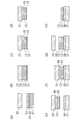
- FIG. 1 is a view conceptually showing a method for manufacturing a device layer transfer substrate according to the present invention.
- an object is to apply to a transmission type LCOS, and in order to obtain a light transmittance with visible light, an Si layer below an embedded oxide film which is an insulator layer is formed by an appropriate method which does not leave a processing mark. It is an object of the present invention to clarify an appropriate transfer method that enables processing without completely removing and thinning a device from wrinkles and peeling from an outer peripheral portion.
- the present invention relates to a method for manufacturing a device layer transfer substrate.
- the manufacturing method includes the following steps (i) to (v). (I) temporarily bonding the device layer side of the SOI wafer including a silicon layer, an insulator layer, and a device layer to a support substrate using a temporary bonding adhesive; (Ii) removing the silicon layer of the SOI wafer until the insulator layer is exposed to obtain a thinned device wafer; (Iii) applying a transfer adhesive to at least one of the exposed insulator layer or the transparent substrate of the thinned device wafer; (Iv) bonding the exposed insulator layer of the thinned device wafer and the transparent substrate via the transfer adhesive; (V) a step of removing the support substrate in a state where the thinned device wafer, the transparent substrate, and the joined body have warpage corrected.
- the device layer transfer substrate is a substrate in which an insulator layer and a device layer manufactured as an SOI (Silicon on Insulator) wafer are bonded to a transparent substrate, and a device layer is provided between the insulator layer and the transparent substrate. It refers to a substrate bonded via an adhesive layer. Therefore, the device layer transfer substrate is a substrate in which a transparent substrate, an adhesive layer, an insulator layer, and a device layer are laminated in this order.
- FIG. 1 is a diagram schematically illustrating a manufacturing method according to the present invention.
- the SOI wafer 14 is a substrate on which a silicon layer 11, an insulator layer 12, and a device layer 13 are stacked in this order.
- the silicon layer 11 is a layer of silicon (Si), and its thickness may be generally about 200 to 1000 ⁇ m, for example, about 750 to 800 ⁇ m for a 300 mm wafer, and about 700 to 750 ⁇ m for a 200 mm wafer.
- the insulator layer 12 is a layer of a buried oxide film (SiO 2 ), and its thickness may be generally about 50 to 500 nm.
- the device layer 13 is a layer in which a pixel electrode and a wiring layer for a micro display are formed on a single crystal silicon (Si) active layer.
- the thickness of the device layer 13 may be usually 2 ⁇ m to 10 ⁇ m, preferably about 4 ⁇ m to 6 ⁇ m, although it depends on the number of wirings.
- an electrode pad for controlling the liquid crystal optionally may be formed on the surface of the device layer 13.
- Such an SOI wafer 14 may be manufactured by an arbitrary method.
- the support substrate 15 used in the temporary bonding step depends on the method of curing the temporary bonding adhesive 16 to be used, but is preferably a substrate having a linear expansion coefficient similar to that of Si.
- a heat-resistant borosilicate glass such as Si wafer, Tempax (registered trademark), or a heat-resistant non-alkali glass such as EAGLE-XG (registered trademark) can be used. Not done.
- a UV-curable acrylic adhesive or an adhesive mainly composed of thermosetting modified silicone can be used.
- WSS manufactured by 3M
- TA1070T, TA2570V3, and TA4070 manufactured by Shin-Etsu Chemical Co., Ltd. can be laminated and used in this order.
- the layers are stacked so that the TA 4070T contacts the support substrate 15 and the TA 1070 contacts the device layer 13.
- the laminated structure of the temporary bonding adhesive 16 may be described as TA1070T / TA2570V3 / TA4070.
- thermosetting modified silicone as a main component
- the adhesive containing thermosetting modified silicone as a main component is excellent in acid resistance and alkali resistance when etching the back surface (silicon layer 11) in the step of obtaining a thinned device wafer following this step.
- the back surface refers to the back surface when the device layer is the front surface.
- the temporary bonding adhesive 16 is applied to the surface of the SOI wafer 14 on which the device layer 13 is formed and / or one main surface of the support substrate 15 by spin coating to a thickness of about 5 to 100 ⁇ m.
- temporary bonding is performed by, for example, UV irradiation or heating.
- the thickness of the temporary bonding adhesive 16 refers to the thickness after curing.
- the adhesive 16 for the temporary bonding is used to separately select an adhesive for protecting the device layer 13, an adhesive for forming a layer to be a release surface, and an adhesive for forming an adhesive layer with the support substrate 15, respectively. They can be used by lamination.
- the laminate obtained by bonding the SOI wafer 14 and the support substrate 15 obtained in this step with the temporary bonding adhesive 16 is also referred to as a temporary bonded body in this specification.
- Step of Obtaining a Thinned Device Wafer a step of obtaining a thinned device wafer is performed.
- the silicon layer 11 of the temporary bonded body is ground and thinned, and the trimmed silicon layer 11, the insulator layer 12, the device layer 13, and the temporary bonding adhesive 16 are edge-trimmed.
- a step of removing the silicon layer 11 remaining after the grinding and thinning step by etching with an acid is performed.
- FIG. 1B is a view conceptually showing a temporary bonded body of the support substrate 15 and the SOI wafer 14 after the silicon layer 11 has been thinly processed.
- the silicon layer 11 can be thinned by processing using a combination of grinding wheels # 600 to # 2000. After the grinding, for example, CMP or dry polishing may be performed to smooth the ground surface.
- the silicon layer 11 it is preferable to leave the silicon layer 11 at about 10 to 100 ⁇ m, preferably about 20 to 50 ⁇ m so that the processing strain due to thinning does not affect the device layer 13. If the remaining silicon layer 11 is thinner than 10 ⁇ m, the processing strain may reach the device layer 13. If the remaining silicon layer 11 is thicker than 100 ⁇ m, the time for removing the remaining silicon layer 11 in the subsequent process, particularly the etching time, becomes longer. The above range is preferable.
- FIG. 1C is a view conceptually showing the temporary joined body after the edge trimming is performed.
- the trimming amount can be determined so that the residue of the temporary bonding adhesive 16 can be sufficiently removed and the area of the device portion is not reduced. Specifically, a portion of about 2 to 5 mm from the edge of the SOI wafer 14 is removed together with the temporary bonding adhesive 16.
- the edge trimming need not be performed.
- Examples of the method of edge trimming include grinding with a grinder and tape polishing with a polishing film.
- modified silicone is used for the temporary bonding adhesive 16, it is particularly preferable to perform edge trimming by tape polishing. This is because, when the grinding is performed by a grinder, the resin for the temporary bonding adhesive 16 containing modified silicone as a main component is soft, so that the grindstone may be clogged, and seizure or peeling of the substrate may occur.
- FIG. 1D is a view conceptually showing a joined body from which the silicon layer 11 has been completely removed.
- Etching can be performed with an acid or an alkali.
- etching with an acid is more preferable, and one or more acids selected from the group consisting of strong acids including HF, HNO 3 , CH 3 COOH, H 2 SO 4 , and H 3 PO 4 , particularly Is most preferably etched with a mixed acid arbitrarily selected and mixed from the group consisting of:
- alkali such as KOH or NH 4 OH
- etching can be performed in a few minutes at room temperature.
- the etching can be performed by immersing the temporary bonded body after the edge trimming or by spin etching on one side. From the viewpoint of suppressing the etching of the support substrate 15, one-side spin etching is preferable.
- the layer of the temporary bonding adhesive 16 is exposed due to the edge trimming.
- the temporary bonding adhesive 16 is not eroded from the edge of the SOI wafer 14 by the etchant. This is particularly advantageous because etching can be performed until the insulator layer 12 is exposed without peeling off.
- the wafer from which the silicon layer 11 obtained in this step is completely removed and the insulator layer 12 is exposed is called a thinned device wafer.
- FIG. 1E is a view conceptually showing a transparent substrate 17 coated with a transfer adhesive 18 and a thinned device wafer bonded to the transparent substrate 17.
- the insulator layer 12 is exposed on the surface of the thinned device wafer from which the silicon layer 11 has been removed in the previous step.
- the thickness of the insulator layer 12 is usually 50 to 500 nm.
- the insulator layer 12 having the above thickness is deformed due to local stress due to the pattern wiring of the device layer 13.
- the transfer adhesive 18 to the transparent substrate 17 side.
- a substrate that is transparent to visible light that is, a substrate that has a transmittance of at least 80%, preferably 85% or more for a wavelength of about 360 to about 840 nm can be used.
- a substrate capable of obtaining a wafer size of 200 to 300 mm ⁇ is preferable, and it is more preferable to use a glass material such as quartz glass, optical glass, and non-alkali glass or sapphire.
- the transfer adhesive 18 an adhesive that is resistant to a maximum process temperature of 200 to 300 ° C. after the formation of the device layer 13 and is transparent to visible light can be used. Transparency with respect to visible light is the same as the definition of transparency in the transparent substrate 18 described above.
- the transfer adhesive 18 minimize the stress applied to the device layer 13 at the time of bonding to the device layer 13, and use an adhesive mainly composed of silicone resin, epoxy-modified rubber, epoxy-modified silicone, or the like. Can be. In particular, it is most preferable to use an adhesive containing epoxy-modified silicone as a main component. This is because the adhesive layer of the transfer adhesive 18 can be formed thin, and has low stress and maintains the adhesive force.
- the layer of the transfer adhesive 18 be formed as thinly and uniformly as possible. This is because the thermal conductivity of the adhesive itself is as small as about 1 W / m ⁇ K, so that deterioration due to heat generation when using the transmission LCOS is reduced.
- the thickness of the layer of the transfer adhesive 18 can be about 0.1 to 5 ⁇ m. If the thickness of the layer of the transfer adhesive 18 exceeds 5 ⁇ m, the heat dissipation may be poor and it may be difficult to remove the heat. Also, if the thickness of the transfer adhesive 18 is less than 0.1 ⁇ m, it is difficult to apply and bond in-plane uniformly and the bonding strength may be weakened.
- the thickness of the layer of the transfer adhesive 18 can preferably be about 0.1 to 2 ⁇ m, more preferably about 0.1 to 1 ⁇ m.
- the thickness of these layers refers to the thickness after curing.
- a method of applying the transfer adhesive 18 a method such as die coating, slit coating, dip coating, or spin coating can be used, but spin coating is most preferable because it can be uniformly applied only to the bonding surface side.
- FIG. 1F is a view conceptually showing a joined body of the thinned device wafer and the transparent substrate 17 joined by the transfer adhesive 18.
- the transfer adhesive 18 preferably applied to the transparent substrate 17 is heated, and the solvent is removed and half-cured. This is to prevent degassing due to heating during joining.
- the temperature range when heating before joining can be, for example, about 100 to 200 ° C., preferably about 120 to 180 ° C.
- the thinned device wafer and the transparent substrate 17 coated with the transfer adhesive 18 are brought into sufficient contact with the bonding surfaces facing each other with a load applied thereto.
- the thinning device wafer and the transparent substrate 17 can be completely bonded by heating while maintaining the load at the time of contact and by fully curing the transfer adhesive 18.
- the upper limit of the applied load may be a load that does not cause deformation of the device layer 13, and is, for example, less than about 20 kgf / cm 2 , preferably about 10 kgf / cm 2 or less, and more preferably about 5 kgf / cm 2 or less.
- a load of about 1 kgf / cm 2 or more is applied so that the transparent substrate 17 and the thinned device wafer can be overlapped while correcting the warpage of about 5 to 50 ⁇ m that can be possessed by each of the thinned device wafer and the transparent substrate 17.
- the warpage of the substrate can be present in both the thinned device wafer and the transparent substrate 17, but this warpage can be corrected by applying a load during bonding.
- the temperature for heating at the time of joining can be appropriately determined according to the curing conditions of the transfer adhesive 18, but is preferably a temperature at which the epoxy group is cured, for example, about 160 to 300 ° C, preferably about 190 to 240 ° C.
- the temperature can be raised to a temperature range of A shorter time for maintaining this temperature range is preferable in terms of throughput. For example, it can be about 1 to 60 minutes, preferably about 2 to 30 minutes, more preferably about 5 to 10 minutes.
- the bonding of the thinned device wafer and the transparent substrate 17 can be performed in any of the atmosphere or the vacuum atmosphere. For example, under a vacuum of about 1E- 1 to 1E- 5 Torr, preferably about 1E- 2 to 1E- 4 Torr. It is preferable to perform bonding. This is because bubbles at the bonding interface do not remain.
- the method of removing the support substrate 15 can be appropriately performed depending on the type of the temporary bonding adhesive 16 used in the previous step.
- a layer is provided that can be easily separated by applying a mechanical force to the bonding surface. . Therefore, the support substrate 15 can be removed by inserting a wedge into one end of the joint surface.
- the transparent substrate 17 When a substrate made of a glass material having a small Young's ratio of about 10 to 80 GPa is used as the transparent substrate 17, an operation of removing the support substrate 15 while fixing the transparent substrate 17 with a vacuum chuck, an electrostatic chuck, or the like may be performed. desirable. This is because the transparent substrate 17 having a small Young's ratio is easily damaged by deformation when the support substrate 15 is removed.
- a step of removing the support substrate 15 with the warp corrected is performed.
- the case where there is a warp means a case where a warp of about 0.2 to 3 mm is visually confirmed and it is difficult to fix the head with a vacuum chuck or an electrostatic chuck or the like as it is.
- the warpage of the substrate before peeling is large, for example, about 1 mm or more, it is possible to eliminate the warp while applying a temperature to the joined body and fix it with a vacuum chuck or the like.
- the temperature in that case depends on the curing temperature of the adhesive used, but may be a temperature of -50 to + 50 ° C.
- the device layer can be transferred without breaking the transparent substrate 17.
- the transparent substrate 17 is a 300 mm glass wafer.
- the device layer can be transferred without breaking the transparent substrate 17.
- there is no warp in the joined body and in that case, there is no need to perform an operation for correcting the warp.
- Manufacturing methods that do not include warpage and do not include a step of correcting warpage are also included in the scope of the present invention.
- FIG. 1H is a view conceptually showing the device layer transfer substrate obtained after the supporting substrate 15 is removed and the residual adhesive 16 for temporary bonding is washed.
- the cleaning and removal of the residue can be performed by immersing the transparent substrate 17 to which the device layer 13 has been transferred in an organic solvent that swells the temporary bonding adhesive 16.
- the organic solvent although it depends on the mode of curing of the temporary bonding adhesive 16, for example, it is preferable to use a hydrocarbon solvent such as p-menthane or a polar solvent such as N-methylpyrrolidone, dimethylformamide, and dimethylsulfoxide. .
- the organic solvent is not limited to these, and can be appropriately selected by those skilled in the art.
- the immersion time is 1 to 10 minutes, preferably 3 to 5 minutes. This method is preferable because the residue can be removed without damaging the device layer 13, particularly without providing a protective layer on the surface of the device layer 13.
- a device layer transfer substrate having a laminated structure of the device layer 13 / insulator layer 12 / transfer adhesive 18 / transparent substrate 17 can be obtained.
- the present invention relates to a device layer transfer substrate.
- the device layer and the insulator layer formed on the SOI (Silicon on Insulator) wafer are bonded via a low-stress adhesive. This is a substrate bonded to a transparent substrate.
- FIG. 1H is a diagram schematically illustrating the device layer transfer substrate according to the present embodiment.
- the device layer transfer substrate has a device layer 13, an insulator layer 12, a transfer adhesive 18, and a transparent substrate 17 laminated in this order.
- the device layer 13 and the insulator layer 12 are layers derived from the device layer 13 and the insulator layer 12 manufactured as an SOI wafer, and the back silicon layer is removed from the SOI wafer by the method described in the first embodiment.
- it is a laminate having a two-layer structure of the device layer 13 and the insulator layer 12. Therefore, the device layer 13 and the insulator layer 12 can be referred to as an insulator layer and a device layer derived from the SOI wafer, or can be referred to as an insulator layer and a device layer formed from the SOI wafer.
- the insulator layer 12 is preferably a buried oxide film (SiO 2 ).
- the thickness of the insulator layer 12 is defined by the thickness of the insulator layer of the SOI wafer on which the device is formed, and the thickness is usually about 50 to 500 nm.
- the device layer 13 is a layer in which a pixel electrode and a wiring layer for a microdisplay are formed on a single crystal silicon (Si) active layer, and the thickness thereof is usually about 4 ⁇ m to 6 ⁇ m.
- the transfer adhesive 18 is a layer formed by curing a low-stress adhesive containing a substance selected from a silicone resin, an epoxy-modified rubber, and an epoxy-modified silicone as a main component, and has a thickness of about 0.1 to 5 ⁇ m.
- the transparent substrate 17 is a substrate transparent to visible light as defined in the first embodiment, and is preferably selected from quartz glass, optical glass, non-alkali glass, and sapphire.
- the device layer transfer substrate having this structure is obtained only by the process of the manufacturing method described above with reference to FIGS. 1A to 1H in the first embodiment.
- a liquid crystal is mounted and sealed with an opposite glass to form a transmission type LCOS panel.
- a transmissive LCOS panel having a layer structure of opposing glass / liquid crystal / ITO / device layer 13 / insulator layer 12 / transfer adhesive 18 / transparent substrate 17 can be obtained. According to the present invention, it is possible to maintain the wafer state until the panel process, and by using a large-diameter wafer of 300 mm, a liquid crystal panel can be formed with good yield and at low cost.
- Example 1 As the device wafer (SOI wafer 14) on which the device layer is formed, the outer dimensions are 300 mm ⁇ , the thickness of the device layer 13 is 4 ⁇ m, the thickness of the buried oxide film (SiO 2 ) as the insulator layer 12 is 250 nm, and the thickness of the silicon layer 11 is 775 ⁇ m.
- the device layer 13 has a configuration in which pixel electrodes and transistors are formed and wiring patterns are stacked.
- An adhesive TA1070T / TA2570V3 / TA4070 manufactured by Shin-Etsu Chemical Co., Ltd. was applied as a temporary bonding adhesive 16 to the surface of the SOI wafer 14 on which the device layer 13 was provided by spin coating.
- 1010 ⁇ m of TA1070T was contacted with the device layer 13 as a device protective layer
- 7 ⁇ m of TA2570V3 was formed as a layer to be a peeling surface of the support substrate 15 after processing
- 90 ⁇ m of TA4070 was laminated as an adhesive layer with the support substrate 15.
- the support substrate 15 As the support substrate 15, an outer diameter of 300 mm in diameter, using a Si wafer having a thickness of 775 .mu.m, a SOI wafer 14 and the supporting substrate 15 coated with a temporary bonding adhesive 16, using a semi-automatic Wehabonda EVG540 made EV Group, 10 - Under a vacuum of 4 Torr, a load of 1 kgf / cm 2 was applied, and held at 140 ° C. for 10 minutes for joining. Thereafter, the joined body of the SOI wafer 14 and the support substrate 15 was treated in an oven at 190 ° C. for 2 hours under normal pressure to cure the temporary bonding adhesive 16.
- the silicon layer 11 on the back surface of the SOI wafer 14 was ground and thinned with a # 2000 grindstone until the thickness became 30 ⁇ m. Although saw marks were observed on the surface after the grinding, peeling and cracking of the wafer and edge chips were not observed.
- edge trimming of the thinned SOI wafer 14 and the temporary bonding adhesive 16 was performed by tape polishing using a wafer edge polishing apparatus NME-123N made of MIPOX.
- the trimming width was 2 mm inward from the outermost periphery of the wafer, and the trimming could be performed without cracking or peeling.
- the silicon layer 11 having a thickness of 30 ⁇ m remaining on the back surface side of the SOI wafer 14 was removed by spin etching with acid using a spin etcher MSE2000 manufactured by Sanmasumi Semiconductor.
- the acid used was a mixed acid of HF / HNO 3 / H 3 PO 4 / H 2 SO 4 , and the silicon layer 11 was completely removed by an etching time of 2 minutes to obtain a thin device wafer.
- a synthetic quartz wafer having an outer diameter of 300 mm ⁇ and a thickness of 775 ⁇ m was used.
- the transfer adhesive 18 TA4070 (manufactured by Shin-Etsu Chemical Co., Ltd.), which is an epoxy-modified silicone adhesive, was diluted with cyclopentanone to prepare a coating solution having an adhesive concentration of 0.5% by weight. This was spin-coated on a quartz wafer prepared as a transparent substrate 17 to form a layer of a transfer adhesive 18 having a thickness of 1 ⁇ m with an in-plane variation of ⁇ 5%.
- the transparent substrate 17 coated with the transfer adhesive 18 was baked at 150 ° C. for 5 minutes to remove the solvent and perform half-curing.
- the insulator layer 12 side of the thinned device wafer and the transparent substrate 17 were joined by using a Tokyo Electron wafer bonder Synapse Si.
- the temperature is raised to 190 ° C.
- a load of 3 kgf / cm 2 is applied, and the device is held at 130 ° C. for 10 minutes under a vacuum of 1E- 4 Torr. And joined.
- the load was removed at a temperature of 60 ° C. or lower, and the joined body in which the transparent substrate 17 and the thinned device wafer were joined was taken out.
- the obtained bonded body of the transparent substrate 17 and the thinned device wafer had a warpage of about 2 mm, it could not be fixed by a vacuum chuck as it was. Therefore, by maintaining the joined body temperature of the transparent substrate 17 and the thinned device wafer at 200 ° C., the warpage was eliminated, and the transparent substrate 17 could be fixed by the vacuum chuck.
- the transparent substrate 17 By fixing the transparent substrate 17 side and inserting a wedge into the temporary bonding interface between the support substrate 15 and the device layer 13 and mechanically peeling off the Si wafer as the support substrate 15, the transparent substrate 17 is not cracked.
- the device layer could be transferred to a certain synthetic quartz wafer having an outer diameter of 300 mm ⁇ . In appearance, there was no peeling of the device layer 13 after the transfer. When the device pattern in the plane was observed with an optical microscope, no cracking or peeling of the pattern was observed.
- the temporary bonding adhesive 16 remaining on the surface of the device layer 13 was removed by immersing the transparent substrate 17 on which the device layer 13 was transferred in p-menthane for 5 minutes. No peeling was observed at the interface between the transferred device layer 13 and the transparent substrate 17, and the transfer adhesive 18 was not eluted by p-menthane.
- the surface of the device layer 13 after the cleaning was observed with an optical microscope, no crack or deformation of the pattern was observed.
- the device layer 13 could be transferred to a synthetic quartz wafer having an outer diameter of 300 mm ⁇ while maintaining the original device pattern shape, and a device layer transfer substrate could be manufactured.
- Example 2 A device wafer (SOI wafer 14) on which the device layer 13 described in Example 1 is formed is prepared, and the same temporary bonding adhesive 16 as in Example 1 is used. Temporary joining was performed. Next, the silicon layer 11 on the back surface of the SOI wafer 14 was completely removed to produce a thin device wafer.
- the transparent substrate 17 is made of Asahi Glass SWAN310, which is an alkali-free glass having an outer diameter of 300 mm ⁇ and a thickness of 775 ⁇ m, using the same transfer adhesive 18 as in Example 1, and using the same procedure as in Example 1 to form an adhesive layer. It was applied and joined.
- the transparent substrate 17 and the thinned device wafer were bonded. No remarkable warpage was observed after joining, and the wafer could be held at room temperature with a vacuum chuck.
- the supporting substrate 15 was peeled off in the same procedure as in Example 1, the device layer 13 could be transferred to a 300 mm non-alkali glass substrate without cracking.
- the device layer 13 after washing was observed with an optical microscope, no cracking or peeling of the pattern was observed, and a device layer transfer substrate could be manufactured.
- Example 3 A device wafer (SOI wafer 14) on which the device layer 13 described in Example 1 is formed is prepared, and the same temporary bonding adhesive 16 as in Example 1 is used. Temporary joining was performed. In the same procedure as in Example 1, a thinned device wafer from which the silicon layer 11 on the back surface of the SOI wafer 14 was completely removed was manufactured. For the transparent substrate 17, EAGLE XG made of Corning, which is an alkali-free glass having an outer diameter of 300 mm ⁇ and a thickness of 775 ⁇ m, was used, and the same transfer adhesive 18 as in Example 1 was used. 18 was applied and joined.
- the thinned device wafer and the transparent substrate 17 were joined. No remarkable warpage was observed after joining, and the wafer could be held at room temperature with a vacuum chuck.
- the supporting substrate 15 was peeled off in the same procedure as in Example 1, the device layer 13 could be transferred to a 300 mm non-alkali glass substrate without cracking.
- the device layer 13 after washing was observed with an optical microscope, no cracking or peeling of the pattern was observed, and a device layer transfer substrate could be manufactured.
- Example 4 A device wafer (SOI wafer 14) on which the device layer 13 described in Example 1 is formed is prepared, and the same temporary bonding adhesive 16 as in Example 1 is used. Temporary joining was performed. In the same procedure as in Example 1, a thinned device wafer from which the silicon layer 11 on the back surface of the SOI wafer 14 was completely removed was manufactured. As the transparent substrate 17, the same quartz wafer as in Example 1 was used. Using the same transfer adhesive 18 as in Example 1, the transfer adhesive 18 was applied not to the transparent substrate 17 but to the insulator layer 12 on the thinned device wafer side in the same procedure as in Example 1.
- Example 5 A device wafer (SOI wafer 14) on which the device layer 13 described in Example 1 was formed was prepared, and temporary bonding with the support substrate 15 was performed using 3M WSS as the temporary bonding adhesive 16.
- WSS is an acrylic UV curing adhesive, which has a layer provided with a layer that is irradiated with a YAG laser and peeled off. Therefore, the support substrate 15 needs to be transparent in the range from UV to near-infrared light.
- a Tempax substrate is used as the support substrate 15.
- Example 2 (4) In the same procedure as in Example 1, the silicon layer 11 on the back surface of the temporary bonded body was ground, edge trimmed, and etched with acid. As a result, the outer peripheral portion of the device wafer after trimming was peeled off, and there was a portion where wrinkles were generated toward the center of the substrate. This is considered to be because the ultraviolet absorbing layer used in the WSS was eroded by the acid and peeled off from the support substrate 15. Since erosion by acid was confirmed, spin etching was attempted at 70 ° C. using 50% KOH, which was an alkali, but peeling occurred on the outer peripheral portion of the device wafer during the etching. In order to completely remove the silicon layer 11 on the back surface of the SOI wafer 14 while holding the bonding between the device wafer and the support substrate 15, the silicone-based temporary bonding adhesive 16 used in Example 1 is more likely to be used. It turned out to be favorable.
- Example 6 A device wafer (SOI wafer 14) on which the device layer 13 described in Example 1 is formed is prepared, and the same temporary bonding adhesive 16 as in Example 1 is used. Temporary joining was performed. Grinding of the back surface of the SOI wafer 14 was performed in the same procedure as in Example 1, and edge trimming with a grinder was attempted. However, the grinding did not proceed in the middle of the edge trimming, and the outer peripheral edge of the device wafer was burned and peeled from the support substrate 15. Although the used temporary bonding adhesive 16 has good resistance to acids and alkalis, it was found that the grinding wheel was clogged and the processing could not proceed. Therefore, it was found that it is more appropriate to perform the edge trimming using the temporary bonding adhesive 16 by tape polishing.
- Example 7 A device wafer (SOI wafer 14) on which the device layer 13 described in Example 1 is formed is prepared, and the same temporary bonding adhesive 16 as in Example 1 is used. Temporary joining was performed. In the same procedure as in Example 1, a thinned device wafer from which the silicon layer 11 on the back surface of the SOI wafer 14 was completely removed was manufactured. As the transparent substrate 17, the same quartz wafer as in Example 1 was used. The application of the transfer adhesive 18 to the transparent substrate 17 was also performed in the same procedure as in Example 1, and the bonding atmosphere was performed under the atmosphere instead of the vacuum.
- Example 1 A device wafer (SOI wafer 14) on which the device layer 13 described in Example 1 is formed is prepared, and the same temporary bonding adhesive 16 as in Example 1 is used. Temporary joining was performed. In the same procedure as in Example 1, a thinned device wafer from which the silicon layer 11 on the back surface of the SOI wafer 14 was completely removed was manufactured. As the transparent substrate 17, the same quartz wafer as in Example 1 was used. Using the same transfer adhesive 18 as in Example 1, the transfer adhesive 18 was applied to a quartz wafer as the transparent substrate 17 in the same procedure as in Example 1, and bonding was performed.
- the bonded wafer had a warp of about 2 mm, a wedge was inserted without removing the warp and the support substrate 15 was peeled off. As a result, the transparent substrate 17 side was broken during peeling, and the device layer 13 could not be transferred to the transparent substrate 17 while maintaining the shape of the wafer. It has been found that it is necessary to fix the transparent substrate 17 side so that no strain is applied to the glass side during peeling.
- Comparative Example 1 it was found that in order to transfer the device layer to the transparent glass substrate without cracking, it was necessary to perform an operation such that the glass substrate was not distorted during peeling.
- an acid-resistant temporary bonding adhesive is more advantageous in removing the silicon layer 11 on the back surface of the wafer.
- edge trimming by tape polishing and apply the transfer adhesive 18 to the transparent substrate 17 side in order to prevent the device wafer from peeling from the support substrate 15 during processing and bonding. I understand. Further, it has been found that it is preferable to examine the bonding atmosphere in order to transfer the entire surface of the wafer.
- the resulting device layer transfer substrate has a device layer / insulator layer / transfer adhesive / transparent substrate, has transparency to visible light, and has a device layer transferred to the entire 300 mm wafer.
- a transmissive LCOS panel at the wafer level by disposing a transparent conductive film such as ITO for controlling the alignment of liquid crystal, a liquid crystal layer, and a counter glass substrate thereon. .
Landscapes
- Physics & Mathematics (AREA)
- Chemical & Material Sciences (AREA)
- General Physics & Mathematics (AREA)
- Nonlinear Science (AREA)
- Theoretical Computer Science (AREA)
- Crystallography & Structural Chemistry (AREA)
- Engineering & Computer Science (AREA)
- Optics & Photonics (AREA)
- Chemical Kinetics & Catalysis (AREA)
- Organic Chemistry (AREA)
- Mechanical Treatment Of Semiconductor (AREA)
- Liquid Crystal (AREA)
- Adhesives Or Adhesive Processes (AREA)
- Weting (AREA)
- Devices For Indicating Variable Information By Combining Individual Elements (AREA)
Abstract
ウェハレベルで実施でき、歩留まりよく且つ大口径で実施することが容易な、デバイス層を透明基板上に転写する方法を提供する。 シリコン層11と絶縁体層12とデバイス層13とを含むSOIウェハ14の前記デバイス層側を、仮接合用接着剤16を用いて支持基板15に仮接合する工程と、前記SOIウェハ14の前記シリコン層11を前記絶縁体層12が露出するまで除去して薄化デバイスウェハを得る工程と、前記薄化デバイスウェハの前記露出した絶縁体層12または透明基板17の少なくとも一方に転写用接着剤18を塗布する工程と、前記転写用接着剤18を介して、前記薄化デバイスウェハの前記露出した絶縁体層12と前記透明基板17とを接合する工程と、前記薄化デバイスウェハと前記透明基板17と接合体に反りがある場合には反りを矯正した状態で前記支持基板15を除去する工程とを含む、デバイス層転写基板の製造方法。
Description
本発明は、液晶装置として、液晶層を挟持する2枚の基板の一方に、単結晶シリコンの回路を透明基板上に形成したLCOSの基板の製造方法ならびにその基板に関するものである。
液晶装置として液晶層を挟持する2枚の基板の一方に単結晶シリコン基板を用いたもの(LCOS;LCD On Silicon)が提案されている。すなわち、トランジスタを形成した単結晶シリコン基板(素子基板)と、ガラス基板(対向基板)との間に液晶層が封入された液晶装置である。LCOSとして、不透明なSOI(Silicon on Insulator)基板を利用した反射型、透明なSOI基板を利用した透過型の液晶装置が提案されている。反射型液晶装置の構成例は特許文献1、透過型の液晶装置の構成例は特許文献2に示されている。反射型の構成では、液晶層を挟持したパネルの外側に反射ミラーや偏光ビームスプリッタなどの光学部品を設ける必要があり、液晶装置の小型化や軽量化を図る上では透過型の液晶装置が有利である。
透過型LCOSは、光が液晶パネルを透過する構成であるため、上記素子基板には光の透過性が求められる。そのため、特許文献2に例示されるように、素子基板として基材が可視光に対し透明なSOI基板、例えばSOS(Silicon on Sapphire)基板、SOQ(Silicon on Quartz)基板、SOG(Silicon on Glass)基板などが用いられる。特にシリコンが単結晶である基板では、素子の移動度が高いため、液晶装置の応答性が早くでき好ましい。シリコン層に画素電極を含むトランジスタを形成した後、対向基板との間に液晶層を挟持させて、透過型LCOSのパネルが製造される。
しかしながら、上記SOI基板にトランジスタを形成する場合、基板が透明且つ絶縁体であるが故に、特に石英基板はシリコンデバイス製造装置の在荷センサーや静電チャックに対応しない問題があり、基板にはそれらに対応する特別な加工が必要となる。また、石英以外のガラス基板はガラス転移温度が低いために、トランジスタの製造が困難である。さらに、SOSを例にとれば、その基板サイズは150mmであるため、コストが高いという問題点がある。コストを下げるためにはサファイア基板のサイズを例えば200mmや300mmに大きくすることが挙げられるが、これらのサイズのサファイア基板は一般的に流通していないため、コストは大きく下がらない問題点がある。
透過型LCOSを製造する手法として、例えばシリコンを基板とするSOI基板に素子層を形成し、その素子層を透明基板に転写する方法が知られている(特許文献3)。すなわちSOI基板上に素子を形成、別基板に接着剤を用いて仮接合、SOIの裏面を除去しチップ化、得られたチップを最終的に搭載する透明基板にアライメントを行い接合、仮接合に用いた基板および接着剤を除去することが述べられている。仮接合に用いる基板としてはガラスが用いられておりその除去にはHFによるエッチング、接着剤の除去には薬液によるエッチングやプラズマエッチングにより実施することが述べられている。特許文献3の方法では仮接合後の基板をダイシングによりチップ化しているため、切断部でチップが接着剤から剥がれが生じやすく、歩留まりが悪くなる問題点があった。さらに上記HFによりガラス基板を除去しているため、最終的に転写する透明基板がガラスである場合、その基板もエッチングする問題があった。さらに接着剤の除去をプラズマエッチング等で実施するため、素子部分をSiN膜等で保護する必要があり、工程数が増えるという問題があった。
本発明は、上記事情に鑑みなされたもので、デバイス層、特にマイクロディスプレイ用の画素電極ならびに配線層を含むデバイス層を透明基板上に転写し、デバイス層転写基板を製造する方法に関するものであり、チップ化せずウェハレベルで実施でき、歩留まりよく且つ大口径で実施することが容易な転写方法ならびに基板を提供することを目的とする。
本発明は、一実施形態によれば、デバイス層転写基板の製造方法であって、
シリコン層と絶縁体層とデバイス層とを含むSOIウェハの前記デバイス層側を、仮接合用接着剤を用いて支持基板に仮接合する工程と、
前記SOIウェハの前記シリコン層を前記絶縁体層が露出するまで除去して薄化デバイスウェハを得る工程と、
前記薄化デバイスウェハの前記露出した絶縁体層または透明基板の少なくとも一方に転写用接着剤を塗布する工程と、
前記転写用接着剤を介して、前記薄化デバイスウェハの前記露出した絶縁体層と前記透明基板とを接合する工程と、
前記薄化デバイスウェハと前記透明基板と接合体に反りがある場合には反りを矯正した状態で前記支持基板を除去する工程と
を含む。
シリコン層と絶縁体層とデバイス層とを含むSOIウェハの前記デバイス層側を、仮接合用接着剤を用いて支持基板に仮接合する工程と、
前記SOIウェハの前記シリコン層を前記絶縁体層が露出するまで除去して薄化デバイスウェハを得る工程と、
前記薄化デバイスウェハの前記露出した絶縁体層または透明基板の少なくとも一方に転写用接着剤を塗布する工程と、
前記転写用接着剤を介して、前記薄化デバイスウェハの前記露出した絶縁体層と前記透明基板とを接合する工程と、
前記薄化デバイスウェハと前記透明基板と接合体に反りがある場合には反りを矯正した状態で前記支持基板を除去する工程と
を含む。
本発明は、別の実施形態によれば、デバイス層転写基板であって、透明基板上に、低応力接着剤を介して、SOIウェハ由来の絶縁体層と、デバイス層とがこの順に積層された基板であって、前記絶縁体層の厚さが50~500nmであり、前記接着剤層の厚さが0.1~5μmである、デバイス層転写基板である。
本発明に係る製造方法によれば、SOIウェハに形成したデバイス層を、チップ化することなくウェハレベルで透明基板に転写することができる。かかる方法は、デバイス層を反転せず転写することが可能である。反転して転写すると、液晶を制御するITOなど透明伝導体を制御する配線をとるため、転写後にビア加工し導電材料で埋め込む加工が必要となる。これに対し、本発明では最上層に透明伝導体と接続するパッドを形成しておけば上述した配線加工が不要となりプロセスを簡素にできる。
以下に、図面を参照して、本発明の実施の形態を説明する。ただし、本発明は、以下に説明する実施の形態によって限定されるものではない。
本発明者らは、鋭意検討の結果、SOIウェハを薄化して薄化デバイスウェハを得るために、極薄チップを形成し三次元積層する際に用いられるウェハ仮接合技術を利用することに想到した。本発明においては、透過型LCOSへの適用を目的としており、可視光での透光性を得るため、絶縁体層である埋め込み酸化膜より下方のSi層を加工痕を残存させない適切な方法で完全に除去し、薄化したデバイスに外周部分から皺が入り、剥離するなどの問題が生じない加工を可能とする、適切な転写方法を明らかにするものである。
[第1実施形態:デバイス層転写基板の製造方法]
本発明は第1実施形態によれば、デバイス層転写基板の製造方法に関する。当該製造方法は、以下の工程(i)~(v)を含む。
(i) シリコン層と絶縁体層とデバイス層とを含むSOIウェハの前記デバイス層側を、仮接合用接着剤を用いて支持基板に仮接合する工程と、
(ii) 前記SOIウェハの前記シリコン層を前記絶縁体層が露出するまで除去して薄化デバイスウェハを得る工程と、
(iii) 前記薄化デバイスウェハの前記露出した絶縁体層または透明基板の少なくとも一方に転写用接着剤を塗布する工程と、
(iv) 前記転写用接着剤を介して、前記薄化デバイスウェハの前記露出した絶縁体層と前記透明基板とを接合する工程と、
(v) 前記薄化デバイスウェハと前記透明基板と接合体に反りがある場合には反りを矯正した状態で前記支持基板を除去する工程。
ここで、デバイス層転写基板とは、SOI(Silicon on Insulator)ウェハとして製造された絶縁体層及びデバイス層が、透明基板に接合された基板であって、絶縁体層と透明基板との間に接着剤層を介して接合された基板をいうものとする。したがって、デバイス層転写基板は、透明基板、接着剤層、絶縁体層及びデバイス層がこの順に積層されてなる基板である。以下、本発明による製造方法を、図1を参照して説明する。図1は、本発明による製造方法を模試的に示す図である。
(i)仮接合工程
仮接合工程では、SOIウェハを支持基板に仮接合する。図1(a)を参照すると、SOIウェハ14は、シリコン層11と絶縁体層12とデバイス層13とがこの順に積層された基板である。シリコン層11はシリコン(Si)の層であり、その厚さは、通常200~1000μm程度であってよく、例えば300mmφのウエハでは、750~800μm程度、200mmφのウエハでは、700~750μm程度であってもよいが、これらには限定されない。絶縁体層12は、埋め込み酸化膜(SiO2)の層であり、その厚さは、通常50~500nm程度であってよい。デバイス層13は、単結晶シリコン(Si)活性層にマイクロディスプレイ用の画素電極および配線層が形成された層である。デバイス層13の厚さは、配線数にもよるが通常2μm~10μm、好ましくは4μm~6μm程度であってよい。デバイス層13の表面には、任意選択的に液晶を制御する電極パッドが形成されていてもよい。このような、SOIウェハ14は、任意の方法で製造されたものであってよい。
仮接合工程では、SOIウェハを支持基板に仮接合する。図1(a)を参照すると、SOIウェハ14は、シリコン層11と絶縁体層12とデバイス層13とがこの順に積層された基板である。シリコン層11はシリコン(Si)の層であり、その厚さは、通常200~1000μm程度であってよく、例えば300mmφのウエハでは、750~800μm程度、200mmφのウエハでは、700~750μm程度であってもよいが、これらには限定されない。絶縁体層12は、埋め込み酸化膜(SiO2)の層であり、その厚さは、通常50~500nm程度であってよい。デバイス層13は、単結晶シリコン(Si)活性層にマイクロディスプレイ用の画素電極および配線層が形成された層である。デバイス層13の厚さは、配線数にもよるが通常2μm~10μm、好ましくは4μm~6μm程度であってよい。デバイス層13の表面には、任意選択的に液晶を制御する電極パッドが形成されていてもよい。このような、SOIウェハ14は、任意の方法で製造されたものであってよい。
仮接合工程で用いる支持基板15は、使用する仮接合用接着剤16の硬化方法にもよるが、Siと同程度の線膨張係数をもつ基板であることが好ましい。支持基板15としては、例えば、Siウェハ、テンパックス(登録商標)などの耐熱性ホウケイ酸ガラス、EAGLE-XG(登録商標)などの耐熱性無アルカリガラスを用いることができるが、これらには限定されない。
仮接合用接着剤16としては、UV硬化アクリル系接着剤や熱硬化性変性シリコーンを主成分とする接着剤を用いることができる。前者としては例えば、WSS(3M製)などを用いることができる。後者としては例えば、信越化学工業株式会社製のTA1070T、TA2570V3、TA4070をこの順に積層して用いることができる。この場合、TA4070Tが支持基板15と接触し、TA1070がデバイス層13と接触するように積層する。以下、本明細書において、この仮接合用接着剤16の積層構成を、TA1070T/TA2570V3/TA4070と記載する場合がある。特には、強酸耐性の熱硬化性変性シリコーンを主成分とする接着剤を仮接合用接着剤として用いることが好ましい。熱硬化性変性シリコーンを主成分とする接着剤は、本工程に続く薄化デバイスウェハを得る工程における、裏面(シリコン層11)エッチング時の酸耐性、ならびにアルカリ耐性に優れるためである。なお、本明細書において、裏面とは、デバイス層をおもて面としたときの裏側の面をいうものとする。
本工程においては、SOIウェハ14のデバイス層13が形成された面、及び/または支持基板15の一方の主面に仮接合用接着剤16をスピンコート法により5~100μm程度に塗布し、使用する仮接合用接着剤16の使用条件により、例えばUV照射あるいは加熱することにより仮接着を行う。仮接合用接着剤16の厚さは、硬化後の厚さをいうものとする。場合により、仮接合用接着剤16は、デバイス層13保護用の接着剤、剥離面となる層を形成する接着剤、支持基板15との接着層を形成する接着剤をそれぞれ別個に選択し、積層して用いることができる。本工程において得られたSOIウェハ14と支持基板15とを仮接合用接着剤16で接着して得られた積層体を、本明細書中において、仮接合体とも指称する。
(ii)薄化デバイスウェハを得る工程
続いて、薄化デバイスウェハを得る工程を実施する。本工程は、仮接合体の前記シリコン層11を研削薄化する工程と、前記研削薄化したシリコン層11、絶縁体層12、デバイス層13、及び前記仮接合用接着剤16をエッジトリミングする工程と、前記研削薄化する工程後に残存するシリコン層11を酸によるエッチングで除去する工程とを含む。
続いて、薄化デバイスウェハを得る工程を実施する。本工程は、仮接合体の前記シリコン層11を研削薄化する工程と、前記研削薄化したシリコン層11、絶縁体層12、デバイス層13、及び前記仮接合用接着剤16をエッジトリミングする工程と、前記研削薄化する工程後に残存するシリコン層11を酸によるエッチングで除去する工程とを含む。
仮接合工程に次いで、支持基板15に仮接合されたSOIウェハ14の裏面のシリコン層11を薄くする。図1(b)は、シリコン層11が薄く加工された後の支持基板15とSOIウェハ14との仮接合体を概念的に示す図である。シリコン層11を薄くする方法としては、スループットの観点から研削によることが好ましい。例えば、#600~#2000の砥石を組み合わせて加工することによりシリコン層11を薄化することができる。研削後に、例えばCMPやドライポリッシュなどを行い、研削面を平滑化してもよい。薄化による加工歪みをデバイス層13まで及ぼさないように、本工程では、シリコン層11を10~100μm程度、好ましくは20~50μm程度残すことが好ましい。残存するシリコン層11が10μmより薄いと、加工歪みがデバイス層13に及ぶおそれがあり、100μmより厚いと、後続の工程で残りのシリコン層11を除去する時間、特にはエッチング時間が長くなるので、上記範囲が好適である。
シリコン層11を前述の程度にまで十分に薄化した後、エッジトリミングを行う。図1(c)は、エッジトリミングを行った後の仮接合体を概念的に示す図である。この工程では、SOIウェハ14の外周部を除去することにより、仮接合用接着剤16の厚さが均一な部分を残す。SOIウェハ14の外周部は面内中央部に比べ仮接合用接着剤16が厚くなる傾向があるためである。トリミング量は、仮接合用接着剤16の残渣を十分に除去でき、且つ、デバイス部分の面積を減らさないように決定することができる。具体的には、SOIウェハ14の縁(エッジ)から、約2~5mmの部分までを、仮接合用接着剤16とともに除去する。なお、支持基板15には仮接合用接着剤16が塗布されていないため、エッジトリミングを行わなくてよい。エッジトリミングの方法としては、グラインダーによる研削、研磨フイルムを用いたテープ研磨等が挙げられる。仮接合用接着剤16に変性シリコーンを用いる場合、テープ研磨にてエッジトリミングを実施することが特に好ましい。グラインダーによる研削を行うと、変性シリコーンを主成分とする仮接合用接着剤16は樹脂が柔らかいため、砥石が目詰まりを起こし、焼きつきや基板の剥がれが発生する場合があるためである。
エッジトリミングに続いて、残存する裏面のシリコン層11を除去するためのエッチングを行う。図1(d)は、シリコン層11が完全に除去された接合体を概念的に示す図である。エッチングは酸またはアルカリによって実施することが可能である。エッチング速度の観点からは、酸によるエッチングがより好ましく、HF、HNO3、CH3COOH,H2SO4、H3PO4を含む強酸からなる群より選択される1以上の酸、特にはこれらから成る群より任意に選択、混合された混酸によるエッチングが最も好ましい。KOHやNH4OHのアルカリによるエッチングでは20μmのSiをエッチングするのに70℃で1時間以上かかるのに対し、上記好ましい酸によるエッチングでは室温において数分でエッチングすることが可能である。エッチングは、エッジトリミングを行った後の仮接合体を浸漬することによって、あるいは片面のスピンエッチングによって実施することが可能である。支持基板15のエッチングを抑制する観点で、片面のスピンエッチングが好ましい。SOIウェハ4の端部ではエッジトリミングを行ったことにより仮接合用接着剤16の層が露出されている。酸に対する耐性がある変性シリコーン系の接着剤を仮接合用接着剤16として用いた場合には、エッチング液により、SOIウェハ14の端部から仮接合用接着剤16が侵食されることが無いため、剥がれが生じることなく、絶縁体層12が露出するまでエッチングすることが可能であり、特に有利である。この工程で得られるシリコン層11が完全に除去され、絶縁体層12が露出したウェハを、薄化デバイスウェハという。
(iii)転写用接着剤を塗布する工程
続いて、薄化デバイスウェハの露出した絶縁体層12または透明基板17の少なくとも一方に転写用接着剤18を塗布する工程を実施する。より好ましくは、透明基板17側に転写用接着剤18を塗布する.図1(e)は、転写用接着剤18が塗布された透明基板17と、これに接合される薄化デバイスウェハを概念的に示す図である。前工程でシリコン層11が除去された薄化デバイスウェハの表面には、絶縁体層12が露出している。絶縁体層12は、通常、50~500nmであるが、シリコン層11が完全に除去されると、デバイス層13のパターン配線による局所的な応力により上記厚さの絶縁体層12が変形し、配線パターンに対応して高さ1~10nmの段差が発生する場合がある。絶縁体層12にこうした段差があると、直接接合やプラズマ接合では、絶縁体層12と透明基板17とを接合することができない。そこで、段差のある面を透明基板17に接合するために、転写用接着剤18を介した接合を行う。通常、転写用接着剤18を塗布すると、溶媒除去のため100~200℃でベーキングをする必要がある。シリコン層11が除去された薄化デバイスウェハを上記温度範囲で加温すると仮接合用接着剤基板16の成分が変形しラメラ状の凹凸が発生し易い。これらのことから、転写用接着剤18は、透明基板17側に塗布することが好ましい。
続いて、薄化デバイスウェハの露出した絶縁体層12または透明基板17の少なくとも一方に転写用接着剤18を塗布する工程を実施する。より好ましくは、透明基板17側に転写用接着剤18を塗布する.図1(e)は、転写用接着剤18が塗布された透明基板17と、これに接合される薄化デバイスウェハを概念的に示す図である。前工程でシリコン層11が除去された薄化デバイスウェハの表面には、絶縁体層12が露出している。絶縁体層12は、通常、50~500nmであるが、シリコン層11が完全に除去されると、デバイス層13のパターン配線による局所的な応力により上記厚さの絶縁体層12が変形し、配線パターンに対応して高さ1~10nmの段差が発生する場合がある。絶縁体層12にこうした段差があると、直接接合やプラズマ接合では、絶縁体層12と透明基板17とを接合することができない。そこで、段差のある面を透明基板17に接合するために、転写用接着剤18を介した接合を行う。通常、転写用接着剤18を塗布すると、溶媒除去のため100~200℃でベーキングをする必要がある。シリコン層11が除去された薄化デバイスウェハを上記温度範囲で加温すると仮接合用接着剤基板16の成分が変形しラメラ状の凹凸が発生し易い。これらのことから、転写用接着剤18は、透明基板17側に塗布することが好ましい。
透明基板17としては、可視光に対し透明である基板、すなわち、約360~約840nmの波長に対して、少なくとも80%、好ましくは85%以上の透過率を有する基板を用いることができる。中でも、200~300mmφのウェハサイズが得られる基板が好ましく、石英ガラス、光学ガラス、無アルカリガラスなどのガラス材料やサファイアを用いることがより好ましい。
転写用接着剤18としては、デバイス層13形成後の最高プロセス温度200~300℃の温度に耐性があり、可視光に対し透明な接着剤を用いることができる。可視光に対し透明とは、上述の透明基板18における透明の定義と同様である。
転写用接着剤18は、デバイス層13との接合時に、デバイス層13への応力が極力小さくなるものが好ましく、シリコーン樹脂、エポキシ変性ゴム、エポキシ変性シリコーンなどを主成分とする接着剤を用いることができる。特には、エポキシ変性シリコーンを主成分とする接着剤を用いることが最も好ましい。転写用接着剤18の接着層を薄く形成することができ、低応力で且つ接着力を保持する点からである。
転写用接着剤18の層は、なるべく薄く且つ均一に形成することが好ましい。接着剤自体の熱伝導率は約1W/m・K程度と小さいので、透過型LCOS使用時の発熱による劣化を小さくするためである。具体的には、転写用接着剤18の層の厚さは約0.1~5μmとすることができる。転写用接着剤18の層の厚さが5μmを超えると、放熱性が悪く除熱しにくくなる場合があるためである。また転写用接着剤18の層の厚さが0.1μm未満では面内均一に塗布し接合することが難しく接合強度が弱くなる場合があるためである。転写用接着剤18の層の厚さは、好ましくは約0.1~2μm、より好ましくは約0.1~1μmとすることができる。なお、これらの層の厚さは、硬化後の厚さをいうものとする。転写用接着剤18を塗布する方法としては、ダイコート、スリットコート、デイップコート、スピンコート等の方法を用いることができるが、接合面側にのみ均一に塗布できる点でスピンコートが最も好ましい。
(iv)絶縁体層と透明基板とを接合する工程
続いて、薄化デバイスウェハにおけるデバイス層13と転写用接着剤18を塗布した透明基板17とを接合する。図1(f)は、転写用接着剤18により接合された薄化デバイスウェハと透明基板17との接合体を概念的に示す図である。接合前に、好ましくは透明基板17に塗布した転写用接着剤18を加温し、溶媒除去およびハーフキュアしておくことが好ましい。接合時の加温による脱ガスを防ぐためである。接合前に加温する際の温度範囲は、例えば、約100~200℃、好ましくは約120~180℃とすることができる。接合前の加温に続いて、薄化デバイスウェハと転写用接着剤18を塗布した透明基板17とを接合面を対向させ荷重をかけ十分に接触させる。次いで、接触時の荷重を保持しつつ加温し、転写用接着剤18をフルキュアすることによって、薄化デバイスウェハと透明基板17とを完全に接合させることができる。印加する荷重の上限は、デバイス層13の変形が生じない荷重であればよく、例えば約20kgf/cm2未満、好ましくは約10kgf/cm2以下、より好ましくは約5kgf/cm2以下である。薄化デバイスウェハ及び透明基板17のそれぞれが有しうる約5~50μmの反りを矯正しつつ、透明基板17と薄化デバイスウェハとを重ね合わせられるよう、約1kgf/cm2以上の荷重をかけることが好ましい。基板の反りは、薄化デバイスウェハ及び透明基板17の双方が有しうるが、接合時に荷重を印加することでこの反りを矯正することができる。
続いて、薄化デバイスウェハにおけるデバイス層13と転写用接着剤18を塗布した透明基板17とを接合する。図1(f)は、転写用接着剤18により接合された薄化デバイスウェハと透明基板17との接合体を概念的に示す図である。接合前に、好ましくは透明基板17に塗布した転写用接着剤18を加温し、溶媒除去およびハーフキュアしておくことが好ましい。接合時の加温による脱ガスを防ぐためである。接合前に加温する際の温度範囲は、例えば、約100~200℃、好ましくは約120~180℃とすることができる。接合前の加温に続いて、薄化デバイスウェハと転写用接着剤18を塗布した透明基板17とを接合面を対向させ荷重をかけ十分に接触させる。次いで、接触時の荷重を保持しつつ加温し、転写用接着剤18をフルキュアすることによって、薄化デバイスウェハと透明基板17とを完全に接合させることができる。印加する荷重の上限は、デバイス層13の変形が生じない荷重であればよく、例えば約20kgf/cm2未満、好ましくは約10kgf/cm2以下、より好ましくは約5kgf/cm2以下である。薄化デバイスウェハ及び透明基板17のそれぞれが有しうる約5~50μmの反りを矯正しつつ、透明基板17と薄化デバイスウェハとを重ね合わせられるよう、約1kgf/cm2以上の荷重をかけることが好ましい。基板の反りは、薄化デバイスウェハ及び透明基板17の双方が有しうるが、接合時に荷重を印加することでこの反りを矯正することができる。
接合時に加温する温度は、転写用接着剤18の硬化条件により適宜決定することができるが、好ましくはエポキシ基が硬化する温度であり、例えば約160~300℃、好ましくは約190~240℃の温度範囲に昇温することができる。この温度範囲を保持する時間は、短い方がスループットの面で好ましい。例えば約1~60分、好ましくは約2~30分、より好ましくは約5~10分とすることができる。薄化デバイスウェハと透明基板17の接合は大気または真空いずれの雰囲気においても実施可能であるが、例えば約1E-1~1E-5Torr、好ましくは約1E-2~1E-4Torrの真空下で接合を行うことが好ましい。接合界面の気泡を残存させないためである。
(v)支持基板を除去する工程
接合に続いて、仮接合していた支持基板15を除去する工程を実施する。これにより、デバイス層13を透明な透明基板17に転写する(図1(g))。支持基板15の除去方法は、先の工程で用いた仮接合用接着剤16の種類により、適宜実施することができる。先に例示した、信越化学工業株式会社製TA1070T/TA2570V3/TA4070の仮接合用接着剤16を用いた場合、機械的な力を接合面に加えることで剥離が容易に行える層が設けられている。このため、接合面の一端に楔を挿入することで支持基板15を除去することができる。透明基板17としてYoung率が約10~80GPaと小さいガラス材料からなる基板を用いる場合には、透明基板17を真空チャックや静電チャック等で固定した状態で支持基板15を外す操作を行うことが望ましい。Young率が小さい透明基板17は、支持基板15を外す際の変形により破損しやすいためである。
接合に続いて、仮接合していた支持基板15を除去する工程を実施する。これにより、デバイス層13を透明な透明基板17に転写する(図1(g))。支持基板15の除去方法は、先の工程で用いた仮接合用接着剤16の種類により、適宜実施することができる。先に例示した、信越化学工業株式会社製TA1070T/TA2570V3/TA4070の仮接合用接着剤16を用いた場合、機械的な力を接合面に加えることで剥離が容易に行える層が設けられている。このため、接合面の一端に楔を挿入することで支持基板15を除去することができる。透明基板17としてYoung率が約10~80GPaと小さいガラス材料からなる基板を用いる場合には、透明基板17を真空チャックや静電チャック等で固定した状態で支持基板15を外す操作を行うことが望ましい。Young率が小さい透明基板17は、支持基板15を外す際の変形により破損しやすいためである。
剥離前の薄化デバイスウェハと透明基板17との接合体に反りがある場合には、反りを矯正した状態で支持基板15を除去する工程を実施する。反りがある場合とは、目視にて、0.2~3mm程度の反りが確認され、そのままでは真空チャックや静電チャック等で固定することが難しい場合をいう。剥離前の基板の反りが大きい場合、例えば、1mm程度以上の場合には、接合体に温度をかけた状態で反りを解消し真空チャックなどで固定することも可能である。その場合の温度は使用する接着剤の硬化温度に依存するが、硬化時の温度に対し-50~+50℃の温度とすることができる。これによって、透明基板17が300mmのガラスウェハである場合にも、透明基板17が割れることなくデバイス層を転写することが可能である。なお、接合体に反りがない場合もあり、その場合には反りを矯正する操作は必要が無い。反りが存在せず、反りを矯正する工程を含まない製造方法も、本発明の範囲に入るものとする。
続いて、デバイス層13の表面に残った仮接合用接着剤16の残渣を洗浄する。図1(h)は支持基板15が除去され、仮接合用接着剤16の残渣洗浄後に得られた、デバイス層転写基板を概念的に示す図である。残渣の洗浄・除去は、デバイス層13を転写した透明基板17を、仮接合用接着剤16を膨潤させる有機溶媒に浸漬させることにより実施することができる。有機溶媒は、仮接合用接着剤16の硬化の態様にもよるが、例えば、p-メンタンなど炭化水素系溶媒や、N-メチルピロリドン、ジメチルホルムアミド、ジメチルスルホキシドなどの極性溶媒を用いることが好ましい。しかしながら、有機溶媒は、これらには限定されず、当業者が適宜選択することができる。浸漬する時間は1~10分、好ましくは3~5分浸漬するとよい。この方法であればデバイス層13にダメージを与えることが無く、特にデバイス層13表面に保護層を設けることなく、残渣の除去を実施することが出来るため好ましい。
以上の工程により、デバイス層13/絶縁体層12/転写用接着剤18/透明基板17の積層構造を持つデバイス層転写基板を得ることができる。
[第2実施形態:デバイス層転写基板]
本発明は、別の実施形態によれば、デバイス層転写基板に関する。特には、第1実施形態において説明した製造方法により製造されたデバイス層転写基板であって、SOI(Silicon on Insulator)ウェハ上に形成したデバイス層と絶縁体層を低応力の接着剤を介して透明基板に接合した基板である。
本発明は、別の実施形態によれば、デバイス層転写基板に関する。特には、第1実施形態において説明した製造方法により製造されたデバイス層転写基板であって、SOI(Silicon on Insulator)ウェハ上に形成したデバイス層と絶縁体層を低応力の接着剤を介して透明基板に接合した基板である。
図1(h)は、本実施形態に係るデバイス層転写基板を模式的に示す図である。デバイス層転写基板は、デバイス層13、絶縁体層12、転写用接着剤18、透明基板17がこの順で積層されている。
デバイス層13及び絶縁体層12は、SOIウェハとして製造されたデバイス層13及び絶縁体層12に由来する層であり、第1実施形態において説明した方法により、SOIウェハから裏面シリコン層が除去され、好ましくはデバイス層13と絶縁体層12との二層構造からなる積層体である。したがって、これらのデバイス層13と絶縁体層12を、SOIウェハ由来の 絶縁体層とデバイス層と指称することができ、あるいはSOIウェハから形成された絶縁体層とデバイス層と指称することもできる。絶縁体層12は、好ましくは埋め込み酸化膜(SiO2)である。絶縁体層12厚は、デバイスを形成したSOIウェハの絶縁体層厚によって規定され、その厚さは、通常、約50~500nmである。デバイス層13は、単結晶シリコン(Si)活性層にマイクロディスプレイ用の画素電極および配線層が形成された層であって、その厚さは、通常、約4μm~6μm程度である。転写用接着剤18は、シリコーン樹脂、エポキシ変性ゴム、エポキシ変性シリコーンから選択される物質を主成分とする低応力接着剤が硬化した層であって、その厚さは約0.1~5μm、好ましくは約0.1~2μm、より好ましくは約0.1~1μmである。透明基板17は、第1実施形態において定義した、可視光に対し透明な基板であって、石英ガラス、光学ガラス、無アルカリガラス、サファイアから選択することが好ましい。この構造を有するデバイス層転写基板は、第1実施形態において図1(a)~(h)を参照しつつ上記で説明した製造方法のプロセスによってのみ得られるものである。
図1(h)に示すデバイス層転写基板には、ITOなどの透明電極をデバイス層13上に形成後、液晶が搭載され、対向ガラスとの間で封止することにより、透過型LCOSパネルを製造することができ、対向ガラス/液晶/ITO/デバイス層13/絶縁体層12/転写用接着剤18/透明基板17の層構成を持つ透過型LCOSパネルが得られる。本発明によればパネル工程まですべてウェハ状態を保つことが可能であり、300mmの大口径ウェハを用いることで、歩留まり良く且つ低コストで液晶パネルを形成することが出来る。
[実施例1]
デバイス層を形成したデバイスウェハ(SOIウェハ14)として、外形300mmφ、デバイス層13の厚さ4μm、絶縁体層12である埋め込み酸化膜(SiO2)の厚さ250nm、シリコン層11の厚さ775μmのウェハを用いた。デバイス層13は画素電極およびトランジスタが形成され、配線パターンが積層された構成とした。
デバイス層を形成したデバイスウェハ(SOIウェハ14)として、外形300mmφ、デバイス層13の厚さ4μm、絶縁体層12である埋め込み酸化膜(SiO2)の厚さ250nm、シリコン層11の厚さ775μmのウェハを用いた。デバイス層13は画素電極およびトランジスタが形成され、配線パターンが積層された構成とした。
このSOIウェハ14のデバイス層13が設けられた面に仮接合用接着剤16として信越化学工業株式会社製の接着剤であるTA1070T/TA2570V3/TA4070をスピンコートにより積層塗布した。まずデバイス保護層としてTA1070Tをデバイス層13に接触して10μm、加工後に支持基板15の剥離面となる層としてTA2570V3を7μm、支持基板15との接着層としてTA4070を90μm積層した。支持基板15としては、外径300mmφ、厚さ775μmのSiウェハを用い、仮接合用接着剤16を塗布したSOIウェハ14と支持基板15とを、EV Group製の半自動ウェハボンダEVG540を用い、10-4Torrの真空下、1kgf/cm2の荷重をかけ、140℃で10分間保持し接合した。その後、SOIウェハ14と支持基板15との接合体を常圧下、190℃で2時間オーブンで処理し、仮接合用接着剤16を硬化させた。
次に、東京精密製のポリッシュ・グラインダPG300を用い、#2000の砥石で、SOIウェハ14の裏面のシリコン層11を、厚さが30μmとなるまで研削し、薄化した。研削後の表面にはソーマークは観察されたものの、ウェハの剥がれや割れ、エッジチップは見られなかった。
続いて、MIPOX製ウェハエッジ研磨装置NME-123Nを用い、テープ研磨にて、薄化したSOIウェハ14と仮接合用接着剤16とのエッジトリミングを実施した。トリミング幅はウェハ最外周から2mm内側までとし、割れや剥がれを生じずトリミングすることができた。
続いて、三益半導体製スピンエッチャーMSE2000を用い、酸によるスピンエッチングによって、SOIウェハ14の裏面側に残存する30μm厚のシリコン層11を除去した。使用した酸はHF/HNO3/H3PO4/H2SO4の混酸であり、2分のエッチング時間でシリコン層11を完全に除去して薄化デバイスウェハを得た。
透明基板17としては、外径300mmφ、厚さ775μmの合成石英ウェハを用いた。転写用接着剤18として、エポキシ変性シリコーン接着剤であるTA4070(信越化学工業株式会社製)をシクロペンタノンで希釈し、接着剤濃度が0.5wt%の塗布液を調製した。これを透明基板17として準備した石英ウェハにスピンコートすることで厚さ1μmの転写用接着剤18の層を面内ばらつき±5%で形成した。転写用接着剤18を塗布した透明基板17を、150℃で5分ベークし、溶媒除去とハーフキュアを行った。
続いて、東京エレクトロン製ウェハボンダーSynapse Siを用いて薄化デバイスウェハの絶縁体層12側と透明基板17とを接合した。転写用接着剤18を塗布した透明基板17と薄化デバイスウェハをチャック後190℃まで昇温し、3kgf/cm2の荷重をかけ、1E-4Torrの真空下130℃で10分保持することにより接合した。その後、60℃以下の温度で荷重を外し、透明基板17と薄化デバイスウェハとが接合された接合体を取り出した。
得られた透明基板17と薄化デバイスウェハとの接合体には約2mmの反りがあったため、そのままでは真空チャックによる固定ができなかった。そのため透明基板17と薄化デバイスウェハとの接合体温度を200℃に保つことで反りが解消され、透明基板17を真空チャック固定することができた。透明基板17側を固定し、支持基板15とデバイス層13との仮接合界面に楔を入れて支持基板15であるSiウェハを機械的に剥がすことにより、割れを生じることなく、透明基板17である外径300mmφの合成石英ウェハにデバイス層を転写することができた。外観上、転写後のデバイス層13の剥がれは無かった。また、光学顕微鏡で面内のデバイスパターンを観察したところ、パターンの割れや剥がれは認められなかった。
デバイス層13の表面に残存した仮接合用接着剤16を、デバイス層13を転写した透明基板17をp-メンタンに5分間浸漬することにより除去した。転写したデバイス層13と透明基板17との界面に剥がれは見られず、転写用接着剤18がp-メンタンにより溶出することは無かった。洗浄後のデバイス層13表面を光学顕微鏡にて観察したところ、パターンの割れや変形は認められなかった。このように、元のデバイスパターン形状を保った状態でデバイス層13を外径300mmφの合成石英ウェハに転写することができ、デバイス層転写基板を製造することができた。
[実施例2]
実施例1に記載のデバイス層13を形成したデバイスウェハ(SOIウェハ14)を準備し、実施例1と同じ仮接合用接着剤16を用い、実施例1と同様の手順で支持基板15との仮接合を行った。次いで、SOIウェハ14裏面のシリコン層11を完全に除去し、薄化デバイスウェハを作製した。透明基板17には、外径300mmφ、厚さ775μmの無アルカリガラスである旭硝子製SWAN310を用い、実施例1と同じ転写用接着剤18を用い、実施例1と同様の手順で、接着層を塗布し接合を実施した。
実施例1に記載のデバイス層13を形成したデバイスウェハ(SOIウェハ14)を準備し、実施例1と同じ仮接合用接着剤16を用い、実施例1と同様の手順で支持基板15との仮接合を行った。次いで、SOIウェハ14裏面のシリコン層11を完全に除去し、薄化デバイスウェハを作製した。透明基板17には、外径300mmφ、厚さ775μmの無アルカリガラスである旭硝子製SWAN310を用い、実施例1と同じ転写用接着剤18を用い、実施例1と同様の手順で、接着層を塗布し接合を実施した。
その結果、透明基板17と薄化デバイスウェハは接合されていた。接合後の顕著な反りは認められず、室温で真空チャックで保持ができた。実施例1と同様の手順で支持基板15を剥離したところ、割れを生じることなく、300mmの無アルカリガラス基板にデバイス層13を転写することができた。洗浄後のデバイス層13を光学顕微鏡で観察したが、パターンの割れや剥がれは見られず、デバイス層転写基板を製造することができた。
[実施例3]
実施例1に記載のデバイス層13を形成したデバイスウェハ(SOIウェハ14)を準備し、実施例1と同じ仮接合用接着剤16を用い、実施例1と同様の手順で支持基板15との仮接合を行った。実施例1と同様の手順で、SOIウェハ14裏面のシリコン層11を完全に除去した薄化デバイスウェハを作製した。透明基板17には、外径300mmφ、厚さ775μmの無アルカリガラスであるCorning製EAGLE XG用い、実施例1と同じ転写用接着剤18を用い、実施例1と同様の手順で転写用接着剤18を塗布し接合を実施した。
実施例1に記載のデバイス層13を形成したデバイスウェハ(SOIウェハ14)を準備し、実施例1と同じ仮接合用接着剤16を用い、実施例1と同様の手順で支持基板15との仮接合を行った。実施例1と同様の手順で、SOIウェハ14裏面のシリコン層11を完全に除去した薄化デバイスウェハを作製した。透明基板17には、外径300mmφ、厚さ775μmの無アルカリガラスであるCorning製EAGLE XG用い、実施例1と同じ転写用接着剤18を用い、実施例1と同様の手順で転写用接着剤18を塗布し接合を実施した。
その結果、薄化デバイスウェハと透明基板17とは接合されていた。接合後の顕著な反りは認められず、室温で真空チャックで保持ができた。実施例1と同様の手順で支持基板15を剥離したところ、割れを生じることなく、300mmの無アルカリガラス基板にデバイス層13を転写することができた。洗浄後のデバイス層13を光学顕微鏡で観察したが、パターンの割れや剥がれは見られず、デバイス層転写基板を製造することができた。
[実施例4]
実施例1に記載のデバイス層13を形成したデバイスウェハ(SOIウェハ14)を準備し、実施例1と同じ仮接合用接着剤16を用い、実施例1と同様の手順で支持基板15との仮接合を行った。実施例1と同様の手順で、SOIウェハ14裏面のシリコン層11を完全に除去した薄化デバイスウェハを作製した。透明基板17は、実施例1と同じ石英ウェハを用いた。実施例1と同じ転写用接着剤18を用い、実施例1と同様の手順で、透明基板17側でなく、薄化デバイスウェハ側の絶縁体層12に転写用接着剤18を塗布した。転写用接着剤18をスピンコートし150℃でベークしたところ、薄化デバイスウェハに皺が入り、支持基板15から剥がれている部分が存在した。透明基板17が接合されておらずデバイスウェハの厚さが薄い状態では、仮接合用接着剤16の熱による変形を抑制することができず皺が入ったものと思われる。従って、転写用接着剤18は薄化デバイスウェハ側に塗布するよりも、透明基板17側に設けることがより好ましいことがわかった。
実施例1に記載のデバイス層13を形成したデバイスウェハ(SOIウェハ14)を準備し、実施例1と同じ仮接合用接着剤16を用い、実施例1と同様の手順で支持基板15との仮接合を行った。実施例1と同様の手順で、SOIウェハ14裏面のシリコン層11を完全に除去した薄化デバイスウェハを作製した。透明基板17は、実施例1と同じ石英ウェハを用いた。実施例1と同じ転写用接着剤18を用い、実施例1と同様の手順で、透明基板17側でなく、薄化デバイスウェハ側の絶縁体層12に転写用接着剤18を塗布した。転写用接着剤18をスピンコートし150℃でベークしたところ、薄化デバイスウェハに皺が入り、支持基板15から剥がれている部分が存在した。透明基板17が接合されておらずデバイスウェハの厚さが薄い状態では、仮接合用接着剤16の熱による変形を抑制することができず皺が入ったものと思われる。従って、転写用接着剤18は薄化デバイスウェハ側に塗布するよりも、透明基板17側に設けることがより好ましいことがわかった。
[実施例5]
実施例1に記載のデバイス層13を形成したデバイスウェハ(SOIウェハ14)を準備し、仮接合用接着剤16として3M製WSSを用い、支持基板15との仮接合を行った。WSSはアクリル系のUV硬化接着剤であり、YAGレーザーを照射し剥離する層を設けた構成である。そのため支持基板15はUV~近赤外で透明である必要があり、ここではテンパックス基板を支持基板15として用いた。
実施例1に記載のデバイス層13を形成したデバイスウェハ(SOIウェハ14)を準備し、仮接合用接着剤16として3M製WSSを用い、支持基板15との仮接合を行った。WSSはアクリル系のUV硬化接着剤であり、YAGレーザーを照射し剥離する層を設けた構成である。そのため支持基板15はUV~近赤外で透明である必要があり、ここではテンパックス基板を支持基板15として用いた。
実施例1と同様の手順で、仮接合体の裏面のシリコン層11を研削し、エッジトリミングを行い、酸によるエッチングを行った。その結果、トリミング後のデバイスウェハ外周部分が剥がれ、基板の中心に向かって皺が発生した部分が存在した。これはWSSに用いられる紫外線吸収層が酸により浸食され、支持基板15から剥がれたためであると考えられる。酸による浸食が確認されたため、アルカリである50%KOHを用い、70℃でスピンエッチングを試みたが、エッチング途中でデバイスウェハの外周部に剥がれが生じた。デバイスウェハと支持基板15との接合を保持した状態でSOIウェハ14裏面のシリコン層11を完全に除去するためには、実施例1で用いたシリコーン系の仮接合用接着剤16がことがより好ましいことがわかった。
[実施例6]
実施例1に記載のデバイス層13を形成したデバイスウェハ(SOIウェハ14)を準備し、実施例1と同じ仮接合用接着剤16を用い、実施例1と同様の手順で支持基板15との仮接合を行った。実施例1と同様の手順でSOIウェハ14裏面の研削まで実施し、グラインダーによるエッジトリミングを試みた。しかしながらエッジトリミングの途中から研削が進まなくなり、デバイスウェハの外周端が焼きつき、支持基板15からの剥がれが発生した。使用した仮接合用接着剤16は酸やアルカリに対する耐性は良好だが、研削の砥石に目詰まりを起こし、加工が進まなくなる場合があることがわかった。したがって、本仮接合用接着剤16を用いてエッジトリミングを行うには、テープ研磨にて実施することがより適していることがわかった。
実施例1に記載のデバイス層13を形成したデバイスウェハ(SOIウェハ14)を準備し、実施例1と同じ仮接合用接着剤16を用い、実施例1と同様の手順で支持基板15との仮接合を行った。実施例1と同様の手順でSOIウェハ14裏面の研削まで実施し、グラインダーによるエッジトリミングを試みた。しかしながらエッジトリミングの途中から研削が進まなくなり、デバイスウェハの外周端が焼きつき、支持基板15からの剥がれが発生した。使用した仮接合用接着剤16は酸やアルカリに対する耐性は良好だが、研削の砥石に目詰まりを起こし、加工が進まなくなる場合があることがわかった。したがって、本仮接合用接着剤16を用いてエッジトリミングを行うには、テープ研磨にて実施することがより適していることがわかった。
[実施例7]
実施例1に記載のデバイス層13を形成したデバイスウェハ(SOIウェハ14)を準備し、実施例1と同じ仮接合用接着剤16を用い、実施例1と同様の手順で支持基板15との仮接合を行った。実施例1と同様の手順で、SOIウェハ14裏面のシリコン層11を完全に除去した薄化デバイスウェハを作製した。透明基板17は、実施例1と同じ石英ウェハを用いた。透明基板17への転写用接着剤18の塗布も実施例1と同様の手順にて実施し、接合の雰囲気を真空ではなく大気下にて実施した。
実施例1に記載のデバイス層13を形成したデバイスウェハ(SOIウェハ14)を準備し、実施例1と同じ仮接合用接着剤16を用い、実施例1と同様の手順で支持基板15との仮接合を行った。実施例1と同様の手順で、SOIウェハ14裏面のシリコン層11を完全に除去した薄化デバイスウェハを作製した。透明基板17は、実施例1と同じ石英ウェハを用いた。透明基板17への転写用接着剤18の塗布も実施例1と同様の手順にて実施し、接合の雰囲気を真空ではなく大気下にて実施した。
得られた薄化デバイスウェハと透明基板17は接合されていたが、支持基板15を剥離したところ、デバイス層13の一部が透明基板17である石英ウェハから浮いている様子が観察された。最表面を洗浄したところ、最表面の仮接合用接着剤16の残澄が無くなったため、デバイス層13の浮いた領域が剥がれた。大気下の接合では、接合界面に気泡が残る場合があり、その部分が接合されない、または接合力が不十分であると考えられる。したがって、面内に均一に転写するには、真空雰囲気にて接合することがより好ましいことがわかった。
[比較例1]
実施例1に記載のデバイス層13を形成したデバイスウェハ(SOIウェハ14)を準備し、実施例1と同じ仮接合用接着剤16を用い、実施例1と同様の手順で支持基板15との仮接合を行った。実施例1と同様の手順で、SOIウェハ14裏面のシリコン層11を完全に除去した薄化デバイスウェハを作製した。透明基板17は、実施例1と同じ石英ウェハを用いた。実施例1と同じ転写用接着剤18を用い、実施例1と同様の手順で転写用接着剤18を透明基板17である石英ウェハに塗布し、接合を行った。
実施例1に記載のデバイス層13を形成したデバイスウェハ(SOIウェハ14)を準備し、実施例1と同じ仮接合用接着剤16を用い、実施例1と同様の手順で支持基板15との仮接合を行った。実施例1と同様の手順で、SOIウェハ14裏面のシリコン層11を完全に除去した薄化デバイスウェハを作製した。透明基板17は、実施例1と同じ石英ウェハを用いた。実施例1と同じ転写用接着剤18を用い、実施例1と同様の手順で転写用接着剤18を透明基板17である石英ウェハに塗布し、接合を行った。
接合済のウェハには約2mmの反りが発生していたが、反りを解消することなくその状態のまま楔を入れ、支持基板15の剥離を試みた。その結果、剥離途中で透明基板17側が割れてしまい、ウェハの形状を保ったままデバイス層13を透明基板17に転写することができなかった。透明基板17側を固定し、剥離中にガラス側に歪がかからないようにする必要があることがわかった。
以上、実施例および比較例の結果を、以下の表1に示す。

上記比較例1により、透明なガラス基板に割れることなくデバイス層を転写するには、剥離時にガラス基板に歪みが生じないような操作をすることが必要であることがわかった。一方、仮接合用接着剤として耐酸性のものを使用することで、ウェハ裏面のシリコン層11の除去において、より有利となることがわかった。さらに、テープ研磨によりエッジトリミングを実施すること、及び透明基板17側に転写用接着剤18を塗布することが、加工時および接合時にデバイスウェハの支持基板15からの剥がれを防ぐには、より好ましいことがわかった。さらに接合をする雰囲気についても検討することがウェハ全面に転写するには好ましいことがわかった。
得られたデバイス層転写基板の構成は、デバイス層/絶縁体層/転写用接着剤/透明基板であり、可視光に対し透光性があり、300mmウェハ全面にデバイス層を転写した基板であった。この基板を用いることにより、その上に液晶の配向を制御するITOなど透明伝導膜、液晶層、対向ガラス基板を配置することにより、ウェハレベルで透過型LCOSのパネルを製造することが可能である。
なお、上記に本実施形態を説明したが、本発明はこれらの例に限定されるものではない。例えば、前述の各実施形態に対して、当業者が適宜、構成要素の追加、削除、設計変更を行ったものや、各実施形態の特徴を適宜組み合わせたものも、本発明の要旨を備えている限り、本発明の範囲に含有される。
11 シリコン層
12 絶縁体層
13 デバイス層
14 SOIウェハ
15 支持基板
16 仮接合用接着剤
17 透明基板
18 転写用接着剤
12 絶縁体層
13 デバイス層
14 SOIウェハ
15 支持基板
16 仮接合用接着剤
17 透明基板
18 転写用接着剤
Claims (14)
- シリコン層と絶縁体層とデバイス層とを含むSOIウェハの前記デバイス層側を、仮接合用接着剤を用いて支持基板に仮接合する工程と、
前記SOIウェハの前記シリコン層を前記絶縁体層が露出するまで除去して薄化デバイスウェハを得る工程と、
前記薄化デバイスウェハの前記露出した絶縁体層または透明基板の少なくとも一方に転写用接着剤を塗布する工程と、
前記転写用接着剤を介して、前記薄化デバイスウェハの前記露出した絶縁体層と前記透明基板とを接合する工程と、
前記薄化デバイスウェハと前記透明基板と接合体に反りがある場合には反りを矯正した状態で前記支持基板を除去する工程と
を含む、デバイス層転写基板の製造方法。 - 前記支持基板を除去する工程が、前記透明基板を固定する工程と、前記支持基板を機械的に剥離する工程とを含む請求項1に記載の方法。
- 前記デバイス層が、マイクロディスプレイ用の画素電極およびその配線層を備えるデバイス層である、請求項1または2に記載の方法。
- 前記薄化デバイスウェハを得る工程が、
前記シリコン層を研削薄化する工程と、
前記研薄化したシリコン層、絶縁体層、デバイス層、及び前記仮接合用接着剤をエッジトリミングする工程と、
前記研削薄化する工程後に残存するシリコン層を酸によるエッチングで除去する工程とを含む、請求項1~3のいずれか1項に記載の方法。 - 前記仮接合用接着剤が、強酸耐性シリコーンを主成分とした変性シリコーン接着剤である、請求項1~4のいずれか1項に記載の方法。
- 前記エッジトリミングする工程がテープ研磨にてなされる、請求項4に記載の方法。
- 前記露出した絶縁体層と前記透明基板とを接合する工程が、荷重下の熱硬化によってなされる、請求項1~6のいずれか1項に記載の方法。
- 前記転写用接着剤が低応力接着剤であり、前記転写用接着剤を塗布する工程において、塗布厚さが0.1μm以上であって5μm以下である、請求項1~7のいずれか1項に記載の方法。
- 前記転写用接着剤が、熱硬化性エポキシ変性シリコーン接着剤である、請求項1~8のいずれか1項に記載の方法。
- 前記透明基板が、石英ガラス、光学ガラス、無アルカリガラス、サファイアから選択される基板である、請求項1~9のいずれか1項に記載の方法。
- 前記SOIウェハに含まれる前記絶縁体層が、埋め込み酸化膜である、請求項1~10のいずれか1項に記載の方法。
- 透明基板上に、低応力接着剤を介して、SOIウェハ由来の絶縁体層と、デバイス層とがこの順に積層された基板であって、前記絶縁体層の厚さが50~500nmであり、前記接着剤層の厚さが0.1~5μmである、デバイス層転写基板。
- 前記低応力接着剤が、熱硬化性エポキシ変性シリコーン接着剤である、請求項12に記載の基板。
- 前記透明基板が、石英ガラス、光学ガラス、無アルカリガラス、サファイアから選択される基板である、請求項12または13に記載の基板。
Applications Claiming Priority (2)
| Application Number | Priority Date | Filing Date | Title |
|---|---|---|---|
| JP2018-128442 | 2018-07-05 | ||
| JP2018128442A JP2020009859A (ja) | 2018-07-05 | 2018-07-05 | デバイス層転写基板の製造方法及びデバイス層転写基板 |
Publications (1)
| Publication Number | Publication Date |
|---|---|
| WO2020008882A1 true WO2020008882A1 (ja) | 2020-01-09 |
Family
ID=69060584
Family Applications (1)
| Application Number | Title | Priority Date | Filing Date |
|---|---|---|---|
| PCT/JP2019/024300 Ceased WO2020008882A1 (ja) | 2018-07-05 | 2019-06-19 | デバイス層転写基板の製造方法及びデバイス層転写基板 |
Country Status (3)
| Country | Link |
|---|---|
| JP (1) | JP2020009859A (ja) |
| TW (1) | TW202025226A (ja) |
| WO (1) | WO2020008882A1 (ja) |
Cited By (1)
| Publication number | Priority date | Publication date | Assignee | Title |
|---|---|---|---|---|
| JP2022191043A (ja) * | 2021-06-15 | 2022-12-27 | 株式会社ディスコ | デバイスの製造方法 |
Families Citing this family (4)
| Publication number | Priority date | Publication date | Assignee | Title |
|---|---|---|---|---|
| JP7780127B2 (ja) * | 2020-03-23 | 2025-12-04 | 日産化学株式会社 | 半導体基板の洗浄方法及び加工された半導体基板の製造方法 |
| JP7635838B2 (ja) * | 2021-05-25 | 2025-02-26 | 信越半導体株式会社 | 化合物半導体接合基板の製造方法 |
| JP7842644B2 (ja) * | 2022-06-07 | 2026-04-08 | 日本放送協会 | 半導体デバイス及びその製造方法 |
| JP2024000113A (ja) * | 2022-06-20 | 2024-01-05 | キオクシア株式会社 | 半導体装置の製造方法 |
Citations (3)
| Publication number | Priority date | Publication date | Assignee | Title |
|---|---|---|---|---|
| JP2010091687A (ja) * | 2008-10-06 | 2010-04-22 | Seiko Epson Corp | 接合方法、接合体および光学素子 |
| JP2015079832A (ja) * | 2013-10-16 | 2015-04-23 | 東京エレクトロン株式会社 | 薄基板の矯正方法および矯正装置 |
| WO2018083961A1 (ja) * | 2016-11-01 | 2018-05-11 | 信越化学工業株式会社 | デバイス層を転写基板に転写する方法および高熱伝導性基板 |
-
2018
- 2018-07-05 JP JP2018128442A patent/JP2020009859A/ja active Pending
-
2019
- 2019-06-19 WO PCT/JP2019/024300 patent/WO2020008882A1/ja not_active Ceased
- 2019-07-04 TW TW108123540A patent/TW202025226A/zh unknown
Patent Citations (3)
| Publication number | Priority date | Publication date | Assignee | Title |
|---|---|---|---|---|
| JP2010091687A (ja) * | 2008-10-06 | 2010-04-22 | Seiko Epson Corp | 接合方法、接合体および光学素子 |
| JP2015079832A (ja) * | 2013-10-16 | 2015-04-23 | 東京エレクトロン株式会社 | 薄基板の矯正方法および矯正装置 |
| WO2018083961A1 (ja) * | 2016-11-01 | 2018-05-11 | 信越化学工業株式会社 | デバイス層を転写基板に転写する方法および高熱伝導性基板 |
Cited By (1)
| Publication number | Priority date | Publication date | Assignee | Title |
|---|---|---|---|---|
| JP2022191043A (ja) * | 2021-06-15 | 2022-12-27 | 株式会社ディスコ | デバイスの製造方法 |
Also Published As
| Publication number | Publication date |
|---|---|
| TW202025226A (zh) | 2020-07-01 |
| JP2020009859A (ja) | 2020-01-16 |
Similar Documents
| Publication | Publication Date | Title |
|---|---|---|
| US11876014B2 (en) | Method of transferring device layer to transfer substrate and highly thermal conductive substrate | |
| WO2020008882A1 (ja) | デバイス層転写基板の製造方法及びデバイス層転写基板 | |
| CN104145330B (zh) | 用于临时接合超薄晶片的方法和装置 | |
| KR101362025B1 (ko) | 고온에서 가요성 반도체 장치를 제공하는 방법 및 그 가요성 반도체 장치 | |
| CN103042803B (zh) | 电子装置的制造方法 | |
| US5160560A (en) | Method of producing optically flat surfaces on processed silicon wafers | |
| US11361969B2 (en) | Device substrate with high thermal conductivity and method of manufacturing the same | |
| CN102034687A (zh) | 键合和转移层的工艺 | |
| CN103548146A (zh) | 用于半导体器件的双有源层及其制造方法 | |
| CN106663640A (zh) | 提供电子器件的方法及其电子器件 | |
| CN116072533B (zh) | 一种晶圆及其晶圆减薄制程加工工艺 | |
| CN108242393B (zh) | 一种半导体器件的制造方法 | |
| CN113454758A (zh) | 半导体元件的制造方法 | |
| JP4728030B2 (ja) | Soiウエーハの製造方法 | |
| CN1690820A (zh) | 器件制造方法 | |
| JP2009537076A (ja) | 絶縁体上半導体構造を形成するための方法 | |
| JP7186921B2 (ja) | 半導体素子の製造方法 | |
| JP4186502B2 (ja) | 薄膜デバイスの製造方法、薄膜デバイスおよび表示装置 | |
| JPH03224266A (ja) | 薄膜素子形成方法及び薄膜素子構造 | |
| WO2014087742A1 (ja) | 半導体装置の製造方法及び半導体装置 |
Legal Events
| Date | Code | Title | Description |
|---|---|---|---|
| 121 | Ep: the epo has been informed by wipo that ep was designated in this application |
Ref document number: 19829996 Country of ref document: EP Kind code of ref document: A1 |
|
| NENP | Non-entry into the national phase |
Ref country code: DE |
|
| 122 | Ep: pct application non-entry in european phase |
Ref document number: 19829996 Country of ref document: EP Kind code of ref document: A1 |