WO2020032036A1 - Boîtier - Google Patents
Boîtier Download PDFInfo
- Publication number
- WO2020032036A1 WO2020032036A1 PCT/JP2019/030933 JP2019030933W WO2020032036A1 WO 2020032036 A1 WO2020032036 A1 WO 2020032036A1 JP 2019030933 W JP2019030933 W JP 2019030933W WO 2020032036 A1 WO2020032036 A1 WO 2020032036A1
- Authority
- WO
- WIPO (PCT)
- Prior art keywords
- housing
- light
- less
- mass
- aluminum oxide
- Prior art date
- Legal status (The legal status is an assumption and is not a legal conclusion. Google has not performed a legal analysis and makes no representation as to the accuracy of the status listed.)
- Ceased
Links
Images



Classifications
-
- C—CHEMISTRY; METALLURGY
- C04—CEMENTS; CONCRETE; ARTIFICIAL STONE; CERAMICS; REFRACTORIES
- C04B—LIME, MAGNESIA; SLAG; CEMENTS; COMPOSITIONS THEREOF, e.g. MORTARS, CONCRETE OR LIKE BUILDING MATERIALS; ARTIFICIAL STONE; CERAMICS; REFRACTORIES; TREATMENT OF NATURAL STONE
- C04B35/00—Shaped ceramic products characterised by their composition; Ceramics compositions; Processing powders of inorganic compounds preparatory to the manufacturing of ceramic products
- C04B35/01—Shaped ceramic products characterised by their composition; Ceramics compositions; Processing powders of inorganic compounds preparatory to the manufacturing of ceramic products based on oxide ceramics
- C04B35/10—Shaped ceramic products characterised by their composition; Ceramics compositions; Processing powders of inorganic compounds preparatory to the manufacturing of ceramic products based on oxide ceramics based on aluminium oxide
- C04B35/111—Fine ceramics
- C04B35/117—Composites
Definitions
- the present disclosure relates to a housing.
- Patent Literature 1 describes Al 2 O 3 , Si, Ti, Mn, Fe, Cr, and the like as an example of the composition of a black ceramic. Fe, Cr, Co, It is described that Mn, Ni, Cu and the like are used.
- the housing of the present disclosure is made of an aluminum oxide ceramic containing an oxide of titanium represented by a composition formula of TiO 2-x (1 ⁇ x ⁇ 2), and contains a total of Fe, Ni, Co, Mn, and Cr. The amount is 260 ppm by mass or less.
- FIG. 1 is a schematic diagram illustrating a configuration of a lamp device including a housing according to an embodiment of the present disclosure, which is mounted on a front right side of a vehicle.
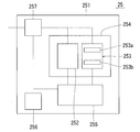
- FIG. 2 is a schematic diagram showing a configuration of a first sensor module arranged in the lamp device shown in FIG.
- FIG. 3 is a schematic diagram illustrating a configuration of a head-up display including a housing according to an embodiment of the present disclosure.
- 4A and 4B show a schematic configuration of a substrate processing apparatus including a housing according to an embodiment of the present disclosure.
- FIG. 4A is a cross-sectional view
- FIG. 4B is a sectional view of a portion surrounded by a two-dot chain line in FIG. It is an enlarged view.
- FIG. 5 is a graph showing the measurement results of the reflectance in the example.
- the housing of the present embodiment is made of an aluminum oxide ceramic containing an oxide of titanium represented by a composition formula of TiO 2-x (1 ⁇ x ⁇ 2), and the total of Fe, Ni, Co, Mn, and Cr is Content is 260 mass ppm or less. According to such a configuration, the reflectance is low over a wide wavelength range. Further, the ultraviolet light (UV) absorption effect of the oxide of titanium can suppress deterioration due to sunlight, and can protect peripheral members of the housing, so that long-term use is possible.
- UV ultraviolet light
- the photocatalytic effect of the oxide of titanium can be exhibited to remove dirt from peripheral members of the housing, and an antifouling effect can be obtained, so that long-term use is possible.
- the configuration of the housing of the present embodiment will be specifically described.
- the aluminum oxide ceramics of all components 100% by mass constituting the ceramics, aluminum oxide content in terms of Al to Al 2 O 3 is at that of the ceramic is 90 mass% or more.
- the oxide of titanium represented by the composition formula TiO 2-x (1 ⁇ x ⁇ 2 ) is obtained by reducing titanium oxide (TiO 2 ).
- the crystal phase of the titanium oxide may be rutile type titanium oxide. Further, the total content of Fe, Ni, Co, Mn and Cr may be 170 mass ppm or less.
- the housing of the present embodiment exhibits black with sufficiently low reflectance for light in a relatively wide wavelength range.
- the lightness index L * in the CIE1976L * a * b * color space is 48 or less, and the chromaticness indices a * and b * are -2 to 5 and -10 to 0, respectively.
- the value of the lightness index L * and the values of the chromaticness indices a * and b * in the CIE1976L * a * b * color space can be determined in accordance with JIS Z8722: 2009.
- a spectral color difference meter (NF777 manufactured by Nippon Denshoku Industries Co., Ltd. or its successor) may be used, and the measurement conditions may be such that the light source is CIE standard light source D65 and the viewing angle is 2 °.
- the maximum value Rmax of the reflectance over a wavelength range of 250 nm to 2500 nm is 24% or less, and the difference ⁇ R between the maximum value Rmax and the minimum value Rmin is 15.3% or less. That is, the housing of the present embodiment has a low reflectance in the wavelength range of 250 nm to 2500 nm and a small variation in the wavelength distribution of the light intensity of the reflected light with respect to the irradiation light. The housing of the present embodiment has a uniformly low reflectance over such a wide wavelength range.
- the content of the titanium oxide represented by the composition formula TiO 2-x (1 ⁇ x ⁇ 2) is, for example, 0.1% of 100% by mass of all components constituting the ceramic. 5 mass% or more and 4 mass% or less.
- the content of the titanium oxide is in the above-described range, a black color having a low reflectance with sufficiently low saturation can be obtained, and the volume resistivity at room temperature (5 to 35 ° C.) can be reduced. It has electrical insulation of 10 9 ⁇ ⁇ m or more.
- the volume specific resistance of the housing of the present embodiment may be, for example, 10 8 ⁇ ⁇ m or more at 200 ° C.
- the volume resistivity decreases as the temperature increases, but the housing of the present embodiment has insulating properties even at a high temperature of 200 ° C.
- the volume resistivity can be determined in accordance with JIS C 2141: 1992.
- the upper limit of the volume resistivity is not particularly limited.
- the aluminum oxide ceramic is inexpensive, and the content of titanium oxide is 0.5% by mass. It is possible to obtain a high dielectric constant equivalent to that of high-purity and expensive aluminum oxide ceramics of less than mass%.
- the housing may not include aluminum titanate.
- XRD X-ray diffractometer
- the total content of Fe, Ni, Co, Mn and Cr is 260 mass ppm or less, that is, the content of Cr alone is 260 mass ppm at the maximum.
- Cr is contained in alumina, light having a wavelength of 700 nm or more and less than 780 nm (hereinafter also referred to as short wavelength light) or light having a wavelength of 780 nm or more and less than 1590 nm (hereinafter referred to as long wavelength light)
- the reflectance of the case of the present embodiment is small in the short wavelength region and the long wavelength region because the content of Cr is small.
- the content of Ni in the housing is 10 ppm by mass or less, the content of Co is 5 ppm by mass or less, or the content of Mn is 100 ppm by mass or less, changes in mechanical strength and electrical characteristics are small. .
- the housing may include silicon, calcium, and magnesium oxide in a grain boundary phase that bonds the aluminum oxide crystal grains.
- the total content of the oxides of silicon, calcium and magnesium is, for example, 2% by mass or more and 4% by mass or less of 100% by mass of all components constituting the ceramics.
- the content of the oxides of calcium and magnesium is 10% by mass or more and 30% by mass or less, and the balance is It may be an oxide of silicon.
- the housing has a volume resistivity at room temperature of 10 11 ⁇ ⁇ m or more, or 10 12 ⁇ ⁇ m or more.
- crystal phase of the oxide of titanium in the housing can be identified by XRD, and the value of x may be determined using a transmission electron microscope (TEM).
- TEM transmission electron microscope
- the contents of aluminum, silicon, calcium, magnesium, and titanium in terms of oxides were determined using an X-ray fluorescence spectrometer (XRF) or an inductively coupled plasma (ICP) emission spectrometer (ICP).
- XRF X-ray fluorescence spectrometer
- ICP inductively coupled plasma
- SiO 2 SiO 2
- CaO CaO
- MgO magnesium oxide
- TiO 2-x (1 ⁇ x ⁇ 2).
- the contents of Fe, Ni, Co, Mn, and Cr may be determined using a glow discharge mass spectrometer (GDMS).
- GDMS glow discharge mass spectrometer
- the housing of the present embodiment may have a portion where the average value of the skewness Rsk is 0.04 or more and 0.45 or less. When the housing has such a portion, the reflectance is low. Note that the average value of all the skewnesses Rsk in the housing may be 0.04 or more and 0.45 or less.
- the housing of the present embodiment may have a portion where the average value of Kurtosis Rku is 4.1 or more and 6.5 or less. When the housing has such a portion, the reflectance is low.
- the average value of all kurtosis Rku in the housing may be 4.1 or more and 6.5 or less.
- the housing of the present embodiment may have a portion where the average value of the arithmetic average roughness Ra is 1 ⁇ m or more and 2 ⁇ m or less.
- the reflectance is low.
- the average value of all arithmetic average roughnesses Ra in the housing may be 1 ⁇ m or more and 2 ⁇ m or less.
- Skewness Rsk, Kurtosis Rku, and arithmetic average roughness Ra can be determined by using, for example, a laser microscope (VK-9510, manufactured by Keyence Corporation) in accordance with JIS B # 0601: 2001.
- the measurement conditions were as follows: the measurement mode was color super-depth, the measurement magnification was 400 times, the measurement range was 698 ⁇ m ⁇ 522 ⁇ m, the measurement pitch was 0.05 ⁇ m, the ⁇ s contour curve filter was 2.5 ⁇ m, and the ⁇ c contour curve filter was 0.08 mm.
- the average value of the measured values obtained from the eight measurement ranges may be the average value of the skewness Rsk, the Kurtosis Rku, and the arithmetic average roughness Ra.
- the aluminum oxide ceramic may have a light-shielding surface, and the color difference ⁇ * Eab of the light-shielding surface in the CIE1976L * a * b * color space may be 4.5 or less.
- the color difference ⁇ * Eab is an index indicating a variation in color tone, and is represented by the following equation (1).
- ⁇ E * ab [( ⁇ L *) 2 + ( ⁇ a *) 2 + ( ⁇ b *) 2 ] 1/2 (1)
- ⁇ L * is the difference between the lightness index L 1 * of the first measurement target point on the light shielding surface and the lightness index L 2 * of the second measurement target point
- ⁇ a * is the chromaticness index of the first measurement target point on the light shielding surface.
- the difference between a 1 * and the brightness index a 2 * of the second measurement point, ⁇ b * is the chromaticity index b 1 * of the first measurement point on the light-shielding surface and the brightness index b 2 * of the second measurement point. Is the difference.
- the variation coefficient of the lightness index L * in the CIE1976L * a * b * color space of the light-shielding surface of the aluminum oxide ceramic may be 0.02 or less (excluding 0).
- the variation coefficient of the lightness index L * is within the above range, the light-shielding surface is hardly discolored even when repeatedly irradiated with light, so that the light-shielding surface does not easily change over time.
- the average value of the lightness index L * of the light-shielding surface is, for example, 48 or less.
- the value of the lightness index L * and the values of the chromaticness indices a * and b * in the CIE1976 L * a * b * color space of the light-shielding surface can be obtained by the same method as described above.
- the aluminum oxide ceramic may have open pores, and the sphericity of the open pore may be 0.1 or more.
- the average value of the equivalent circle diameter of the open pores is, for example, 4 ⁇ m or more and 6 ⁇ m or less.
- the porosity of the open pores is 3 area% or more and 6 area% or less.
- the average particle diameter D 50 was polished holding member in the cast iron plate with diamond abrasive grains of 3 [mu] m, an average particle diameter D 50 0. Polishing is performed on a tin platen using diamond abrasive grains of 5 ⁇ m to obtain a measurement surface.
- an average part of the measurement surface is selected and photographed with a CCD camera at a magnification of 100 using an optical microscope.
- image analysis software for example, Win ROOF, manufactured by Mitani Corporation
- the threshold value of the equivalent circle diameter of the open pores is 0.8 ⁇ m, and the equivalent circle diameter less than 0.8 ⁇ m is not analyzed.
- the skewness of the circle equivalent diameter of the open pore may be obtained by using a function SKEW provided in Excel (registered trademark, Microsoft Corporation).
- the shape of the housing is not particularly limited, and a desired shape can be adopted according to a member to be housed.
- powders of aluminum oxide, silicon oxide, calcium carbonate, magnesium hydroxide and titanium oxide are prepared.
- the total content of the powders of calcium carbonate, magnesium hydroxide, and silicon oxide is, for example, 6.5% by mass or more and 12.9% by mass or less of the total 100% by mass of the powder.
- the content of the powder of calcium carbonate, magnesium hydroxide and silicon oxide is 17.8% by mass or more and 53.4% by mass or less of the total of 100% by mass of these powders.
- the content of the magnesium hydroxide powder is 14.4% by mass or more and 43.2% by mass or less, and the remainder is silicon oxide powder.
- the content of the titanium oxide powder is, for example, 0.5% by mass or more and 4% by mass or less of the total 100% by mass of each powder of aluminum oxide, silicon oxide, calcium carbonate, magnesium hydroxide, and titanium oxide;
- the balance is aluminum oxide powder.
- the content of magnesium hydroxide is preferably 30% by mass or more and 44% by mass or less of the content of titanium oxide.
- the content of magnesium hydroxide is in the above range, generation of anorthite and mullite which are likely to occur in a reduction treatment described later is suppressed. Since anorthite and mullite have different average coefficients of linear expansion from aluminum oxide, if the formation of these compounds is suppressed, cracking occurs even when the housing is used in an environment that is repeatedly exposed to heating and cooling. Is less likely to occur.
- a pulverizer such as a barrel mill, a rotary mill, a vibration mill, a bead mill, an agitator mill, an atomizer, and an attritor to obtain a slurry.
- a solvent, an organic binder such as polyvinyl alcohol (PVA) in an amount of 1 part by mass to 1.5 parts by mass with respect to 100 parts by mass of the solvent, and 0.1 part by mass with respect to 100 parts by mass of the solvent Parts by mass and 0.5 part by mass or less of the dispersant are put into the grinder together.
- PVA polyvinyl alcohol
- the obtained slurry is subjected to a demagnetization treatment and then spray-dried to obtain granules.
- Fe, Ni and Co which are ferromagnetic metals, are removed.
- the contents of Fe, Ni, Co, Mn and Cr in the housing are affected by the wear of the stainless steel member used in the pulverizer.
- a stainless steel member that is worn by long-term use may be replaced with a titanium component that easily forms a passivation film on its surface, or a titanium-based film such as TiN, TiCN, TiC, TiAlN, TiAlCN, or TiAlO, or a non-titanium-based material.
- the surface of the stainless steel member may be coated with crystalline hard carbon (DLC).
- a molded article is formed by a dry pressure molding method or a molded article is formed by a cold isostatic pressing method (CIP) followed by cutting.
- CIP cold isostatic pressing method
- the molding pressure may be, for example, 1500 MPa or more and 4000 MPa or less.
- the obtained compact is fired in an air (oxidizing) atmosphere at a temperature of 1500 ° C. or higher and 1700 ° C. or lower for a predetermined time to fire, thereby obtaining a sintered body.
- the sintered body obtained by the above-described method is used as a reducing atmosphere, for example, in a mixed gas having a nitrogen: hydrogen ratio of 87 to 90% by volume: 10 to 13% by volume, from 1300 ° C. to 1400 ° C.
- a mixed gas having a nitrogen: hydrogen ratio of 87 to 90% by volume: 10 to 13% by volume from 1300 ° C. to 1400 ° C.
- the housing of the present embodiment described above has low reflectance in the visible light region and the (near) infrared region, and can be used for a long period of time.
- a lamp device and a head-up display will be described as an example of a vehicle-mounted optical device including the housing of the present embodiment, and the description will be sequentially given with reference to the drawings.
- the in-vehicle optical device according to the present disclosure may include any configuration that is not illustrated in the drawings referred to. Further, the dimensions of the components in the drawings do not faithfully represent the dimensions, dimensional ratios, and the like of the actual components.
- Lamp device In the following description, a configuration in which the lamp device is mounted on the right front of the vehicle will be described as an example, but the lamp device of the present disclosure is not limited to a configuration mounted on the right front of the vehicle as long as it has the function.
- a lamp device 20 includes a light-transmitting cover 21 located in a traveling direction of a vehicle, a housing 22 located on the opposite side of the light-transmitting cover 21, and a light-transmitting cover 21. And a headlight 24, a first sensor module 25, and a second sensor module 26 which are respectively located inside a lamp room 23 surrounded by the housing 22.
- the headlight 24 includes an optical system component including at least one of a lens and a reflector.
- the light emitted from the headlight 24 passes through the translucent cover 21 and illuminates the right front of the vehicle. Since the lamp device 20 includes such a headlight 24, it functions as a headlight.
- the first sensor module 25 includes a first substrate 251 (support member).
- the first substrate 251 supports a first visible light camera 252, a first LiDAR (Light Detection and Ranging) sensor 253, and a first light shielding member 254 (shielding member). Further, as shown in FIG. , A communication unit 256 and a power supply unit 257.
- the first substrate 251 is a substrate on which a sensor circuit including the first visible light camera 252, the first LiDAR sensor 253, the control unit 255, the communication unit 256, and the power supply unit 257 is mounted.
- a plurality of sensors (the first visible light camera 252 and the first LiDAR sensor 253) having different detection methods, a first light-blocking member 254 which is a cylindrical hollow member surrounding these sensors, and a circuit for operating these sensors are modularized on the first substrate 251.
- the first visible light camera 252 captures an image of the right side of the vehicle. That is, the first visible light camera 252 is a sensor that detects information on the right side of the vehicle.
- the first LiDAR sensor 253 includes a light emitting unit 253a that emits infrared light and a light receiving unit 253b that detects reflected light that is reflected by the infrared light hitting an object present on the right side of the vehicle.
- the first LiDAR sensor 253 can calculate the distance to the object based on the time from emitting infrared light in a certain direction to detecting reflected light from the object.
- information on the shape of the object can be obtained by collecting and analyzing the measured values of the distance in association with the detected position.
- information such as the material of the object associated with the reflection can be obtained based on the difference between the wavelengths of the emitted light and the reflected light.
- information on the color of the target object (such as a white line on the road surface) can be obtained based on the difference in the reflectance of the reflected light. That is, the first LiDAR sensor 253 can obtain various information on the right side of the vehicle by a method different from that of the first visible light camera 252.
- the first sensor module 25 includes a first actuator 258 (an example of an adjustment mechanism) coupled to the first substrate 251.
- the first actuator 258 adjusts at least one of the position and the posture of the first substrate 251 with respect to the vehicle.
- the second sensor module 26 includes the second substrate 261.
- the second substrate 261 supports the second visible light camera 262, the second LiDAR sensor 263, the millimeter wave radar 264, and the second light shielding member 265 which is a cylindrical hollow member surrounding these, all of which are not shown.
- the control unit, the communication unit, and the power supply unit are further supported.
- the functions of the second visible light camera 262 and the second LiDAR sensor 263 are the same as the functions of the first visible light camera 252 and the first LiDAR sensor 253, respectively, and a description thereof will be omitted.
- the millimeter-wave radar 264 includes a transmitting unit that transmits a millimeter wave and a receiving unit that receives a reflected wave that has been reflected by at least an object in which the millimeter wave hits the right front of the vehicle.
- the frequency of the millimeter wave is, for example, 24 GHz, 26 GHz, 76 GHz, or 79 GHz.
- the millimeter-wave radar 264 can determine the distance to the object based on the time from when the infrared light is emitted in a certain direction to when the reflected light from the object is detected. In addition, by collecting and analyzing the distance measurement values in association with the detection position, information relating to the movement of the object can be obtained. That is, the millimeter wave radar 264 can obtain information on the right front of the vehicle by a method different from that of the second visible light camera 262 or the second LiDAR sensor 263.
- the second sensor module 26 includes a second actuator 266 (an example of an adjustment mechanism) coupled to the second substrate 261.
- the second actuator 266 adjusts at least one of the position and the posture of the second substrate 261 with respect to the vehicle.
- the lamp device 20 also includes a signal processing unit 27 located outside the lamp room 23.
- the signal processing unit 27 is configured to output a first drive signal 271 for driving the first actuator 258 and a second drive signal 272 for driving the second actuator 266.
- the first drive signal 271 includes at least one of the position and the posture of the first actuator 258, and the second drive signal 272 includes the information of at least one of the position and the posture of the second actuator 266. .
- the lamp device 20 further includes the following configuration in addition to the configuration described above. That is, the lamp device 20 includes a housing that houses the lens of the first visible light camera 252. Then, in the lamp device 20, the housing for housing the lens of the first visible light camera 252 comprises the above-described housing of the present embodiment. In other words, the housing of the present embodiment may be for a vehicle-mounted camera. According to such a configuration, the noise of the projected image can be reduced by the low reflectance in the visible light region and the (near) infrared region of the housing of the present embodiment. In addition, the sensitivity can be maintained by preventing contamination near the lens by the photocatalytic effect of the oxide of titanium.
- the lamp device 20 includes a housing for housing the light source element of the first LiDAR sensor 253 and a housing for housing the light receiving element of the light receiving section 253b of the first LiDAR sensor 253.
- the housing of the present embodiment may be for LiDAR. According to such a configuration, noise can be reduced by the low reflectance in the near-infrared region of the housing of the present embodiment, and as a result, the detection performance of the first LiDAR sensor 253 is enhanced.
- the photocatalytic effect of the oxide of titanium can prevent contamination of the light source element in the first LiDAR sensor 253 and maintain the sensitivity.
- the lamp device 20 also includes the same housing as the first visible light camera 252 and the first LiDAR sensor 253 described above for the second visible light camera 262 and the second LiDAR sensor 263.
- the housing of the second visible light camera 262 and the second LiDAR sensor 263 may be configured by the housing of the present embodiment.
- the head-up display 30 includes an in-vehicle projector module 31, a reflection mirror 32, a microlens array 33, a convex lens 34, a combiner 35.
- the vehicle-mounted projector module 31 projects an image in the direction of arrow a.
- the in-vehicle projector module 31 includes an optical and MEMS (Micro Electro Mechanical Systems) unit and an RGB light source module housed in the optical and MEMS unit.
- MEMS Micro Electro Mechanical Systems
- the reflection mirror 32 reflects the image projected from the vehicle-mounted projector module 31 toward the microlens array 33.
- the micro lens array 33 functions as an intermediate image screen.
- the convex lens 34 is adjacent to the microlens array 33 and convex toward the combiner 35, and functions as a field lens.
- the combiner 35 reflects the image enlarged by the convex lens 34 toward the driver's eyes.
- the micro lens array 33 and the convex lens 34 are held by a lens holding member 36. That is, the head-up display 30 includes the lens holding member 36 that holds the micro lens array 33 and the convex lens 34.
- the head-up display 30 further includes the following configuration in addition to the configuration described above. That is, the head-up display 30 includes a housing located around the light source member of the vehicle-mounted projector module 31 (optical or MEMS unit).
- the housing of the vehicle-mounted projector module 31 (optical or MEMS unit) is the housing of the present embodiment.
- the housing of the present embodiment may be for a head-up display. According to such a configuration, noise of a projected image can be reduced by a low reflectance over a wide wavelength range of the housing of the present embodiment.
- the antifouling effect of the photocatalytic effect of the oxide of titanium enables long-term use.
- the housing of the present embodiment can be used for a semiconductor manufacturing apparatus.
- the semiconductor manufacturing apparatus is a plasma processing apparatus that forms a film on a substrate such as a semiconductor wafer W (hereinafter, a semiconductor wafer is referred to as a wafer) using plasma.
- a substrate such as a semiconductor wafer W (hereinafter, a semiconductor wafer is referred to as a wafer) using plasma.
- An example in which a titanium film is formed on a wafer W using the plasma processing apparatus 40 will be described.
- the plasma processing apparatus 40 includes a cylindrical processing container 41 having an open top, and a mounting member 42 provided in the processing container 41 for mounting the wafer W. I have.
- the processing container 41 is electrically grounded by an earth wire 43 connected to the processing container 41.
- the mounting member 42 is made of aluminum nitride ceramics, and is provided with a film (not shown) made of a conductive material on its surface, for example, is an electrostatic chuck.
- the mounting member 42 is supported by a support member 44 made of a conductive material, and is electrically connected to the support member 44.
- the support member 44 is installed inside the processing container 41 and is electrically connected to the processing container 41. Therefore, the mounting member 42 is grounded via the processing container 41, and functions as a lower electrode arranged to face the disk-shaped upper electrode 45.
- the first heater 46 for heating the wafer W is built in the mounting member 42.
- the upper electrode 45 has a plurality of through holes 45 a for supplying a plasma generation gas from a gas supply source 47.
- the plasma generation gas is, for example, TiCl 4 gas, H 2 gas, and Ar gas.
- the upper electrode 45 has an extension 45b extending upward on the outer peripheral side.
- the outer peripheral surface of the extension part 45b is separated from the inner peripheral surface of the processing container 41.
- the outer diameter of the upper electrode 45 facing the mounting member 42 is larger than the outer diameter of the wafer W so as to cover the entire surface of the wafer W mounted on the mounting member 42.
- a disk-shaped lid 48 is placed on the upper end surface of the extension 45b, and a gas diffusion section 49 is formed as a space surrounded by the lid 48 and the upper electrode 45.
- the lid 48 is made of a conductive material such as nickel.
- the lid 48 is provided with a locking portion 48 a extending toward the outer peripheral side on the upper surface side of the lid 48.
- the locking portion 48 a has a step in the thickness direction, and is held by an annular holding member 50 supported by the processing container 41.
- the holding member 50 is made of, for example, an insulating material such as quartz, and the upper electrode 45 and the processing container 41 are electrically insulated.
- a second heater 51 is provided outside the lid 48. The upper electrode 45 and the lid 48 placed on the upper end surface of the extension 45b are heated by the second heater 51.
- an annular casing 52 of the present disclosure is provided on the outer peripheral side of the extension 45 b so as to surround the upper electrode 45, and between the upper electrode 45 and the casing 52.
- the lower end surface of the housing 52 is set to have the same height in the vertical direction as the lower end surface of the upper electrode 45, and when a high frequency is applied between the lower electrode and the upper electrode 45, the processing is performed.
- the plasma generated in the container 41 is not unevenly distributed.
- the housing 52 is held by the holding member 50, and has a gap between the outer peripheral surface and the inner peripheral surface of the processing container 41.
- the housing 52 has an internal space 52a along the circumferential direction, and the upper part of the housing 52 is sealed by an annular sealing member 53.
- a heating mechanism 54 such as an electric (infrared) heater is arranged along the circumferential direction.
- the surface temperature of the housing 52 can be relatively increased.
- the TiCl 4 gas supplied into the container 41 is turned into plasma by heating by the first heater 46, the second heater 51, and the heating mechanism 54, and impurities such as decomposed Cl ions and radicals which are likely to remain in the titanium film. Removal efficiency is increased, and a high quality titanium film can be obtained.
- the housing is used for the in-vehicle optical device and the semiconductor manufacturing device.
- the housing of the present embodiment is limited to the in-vehicle optical device and the semiconductor manufacturing device. It can be used for other purposes as well.
- Other applications include, for example, electronic equipment, medical and physicochemical equipment, and the like. Specific examples include medical equipment such as CT scanning, and analyzers such as a transmission electron microscope (TEM).
- TEM transmission electron microscope
- the use of the housing is not limited to the illustrated one.
- the granules were formed by cold isostatic pressing (CIP) and then subjected to cutting to obtain a formed body. Thereafter, the obtained molded body was kept in an air (oxidizing) atmosphere at a temperature of 1570 ° C. for 2 hours to obtain a sintered body. Next, the surface of the sintered body was polished using a vibration barrel polishing machine.
- CIP cold isostatic pressing
- the sintered body obtained by the above-described method is kept at a temperature of 1350 ° C. for 1 hour and 30 minutes in a reducing atmosphere (a mixed gas having a nitrogen: hydrogen ratio of 88.5% by volume: 11.5% by volume).
- a mixed gas having a nitrogen: hydrogen ratio of 88.5% by volume: 11.5% by volume As a result, the sample No. 1-4 were obtained.
- Each of the obtained samples was identified using XRD.
- the value of x in TiO 2-x was determined using a transmission electron microscope (TEM). Further, the contents of the elements constituting each sample were determined using XRF, and converted into the identified components. Further, the contents of the trace components Fe, Ni, Co, Mn and Cr were determined using a glow discharge mass spectrometer (GDMS). Table 1 shows the results. Each sample contains inevitable impurities as components not shown in Table 1.
- the reflectance in the wavelength range of 250 nm to 2500 nm was determined using an ultraviolet-visible-near-infrared spectrophotometer (V-670, manufactured by JASCO Corporation), and the measured values were graphed. 5 is shown. Further, ⁇ R was calculated from the minimum value Rmin and the maximum value Rmax of the reflectance in the above-mentioned region of each sample. Table 1 shows the minimum value Rmin, the maximum value Rmax, and ⁇ R of the reflectance.
- the integrating sphere unit used for the measurement of the reflectance is ISN-723
- the reference light source is a deuterium lamp in a wavelength region of 250 nm to 360 nm
- the halogen lamp is a region in a wavelength range of 360 nm to 2500 nm.
- the mode was total reflectance
- the data acquisition interval was 1.0 nm
- the UV / Vis bandwidth was 5.0 nm
- the NIR bandwidth was 20.0 nm.
- Sample Nos. 1 to 3 are sample Nos. Rmax and ⁇ R were smaller than 4. From these results, it was made of an aluminum oxide ceramic containing a titanium oxide represented by a composition formula of TiO 2-x (1 ⁇ x ⁇ 2), and the total content of Fe, Ni, Co, Mn and Cr was 260 It was found that when the mass was ppm or less, the reflectance was low in the wavelength range of 250 nm to 2500 nm, and the variation in the wavelength distribution of the light intensity of the reflected light with respect to the irradiation light was small.
- sample no. No. 1 is more suitable for use as described above because the difference ⁇ R in the reflectance in the above-mentioned region is 6.2%.
Landscapes
- Chemical & Material Sciences (AREA)
- Engineering & Computer Science (AREA)
- Ceramic Engineering (AREA)
- Composite Materials (AREA)
- Manufacturing & Machinery (AREA)
- Materials Engineering (AREA)
- Structural Engineering (AREA)
- Organic Chemistry (AREA)
- Compositions Of Oxide Ceramics (AREA)
Abstract
Ce boîtier est formé à partir d'une céramique à base d'oxyde d'aluminium contenant un oxyde de titane représenté par la formule de composition TiO2-x(1 ≤ x <2). La teneur totale en Fe, Ni, Co, Mn et Cr est de 260 ppm en masse ou moins.
Priority Applications (1)
| Application Number | Priority Date | Filing Date | Title |
|---|---|---|---|
| JP2020535796A JPWO2020032036A1 (ja) | 2018-08-08 | 2019-08-06 | 筐体 |
Applications Claiming Priority (2)
| Application Number | Priority Date | Filing Date | Title |
|---|---|---|---|
| JP2018-149444 | 2018-08-08 | ||
| JP2018149444 | 2018-08-08 |
Publications (1)
| Publication Number | Publication Date |
|---|---|
| WO2020032036A1 true WO2020032036A1 (fr) | 2020-02-13 |
Family
ID=69413558
Family Applications (1)
| Application Number | Title | Priority Date | Filing Date |
|---|---|---|---|
| PCT/JP2019/030933 Ceased WO2020032036A1 (fr) | 2018-08-08 | 2019-08-06 | Boîtier |
Country Status (2)
| Country | Link |
|---|---|
| JP (1) | JPWO2020032036A1 (fr) |
| WO (1) | WO2020032036A1 (fr) |
Citations (5)
| Publication number | Priority date | Publication date | Assignee | Title |
|---|---|---|---|---|
| JP2000327405A (ja) * | 1999-05-11 | 2000-11-28 | Sumitomo Metal Electronics Devices Inc | 着色アルミナ質焼結体 |
| JP2006182595A (ja) * | 2004-12-27 | 2006-07-13 | Nippon Tungsten Co Ltd | 暗色多孔質焼結体およびその製造方法 |
| JP2016176988A (ja) * | 2015-03-18 | 2016-10-06 | 京セラ株式会社 | 低反射部材 |
| WO2018139673A1 (fr) * | 2017-01-30 | 2018-08-02 | 京セラ株式会社 | Élément céramique semi-conducteur et support pour transport de plaquette |
| JP2018142462A (ja) * | 2017-02-28 | 2018-09-13 | 京セラ株式会社 | セラミック絶縁部材および電子管 |
Family Cites Families (9)
| Publication number | Priority date | Publication date | Assignee | Title |
|---|---|---|---|---|
| JPS5432450B2 (fr) * | 1972-07-11 | 1979-10-15 | ||
| JPS51113197A (en) * | 1975-03-28 | 1976-10-06 | Hitachi Chem Co Ltd | Black ceramics for electronic parts |
| JPH0493878U (fr) * | 1990-12-28 | 1992-08-14 | ||
| JP2541066Y2 (ja) * | 1991-09-27 | 1997-07-09 | 株式会社島津製作所 | ヘッドアップディスプレイ |
| JP5004573B2 (ja) * | 2006-12-25 | 2012-08-22 | 京セラ株式会社 | 半導体製造装置用耐食性部材およびその製造方法 |
| CN101265106A (zh) * | 2008-03-24 | 2008-09-17 | 宁波工程学院 | 一种制备纳米/纳米型Si3N4/SiC纳米复相陶瓷的方法 |
| JP5665988B2 (ja) * | 2011-07-14 | 2015-02-04 | 京セラ株式会社 | 回路基板および電子装置 |
| JP5726279B2 (ja) * | 2013-12-06 | 2015-05-27 | 株式会社トクヤマ | 窒化アルミニウム粉末 |
| JP6824909B2 (ja) * | 2015-06-02 | 2021-02-03 | サイエンティフィック・デザイン・カンパニー・インコーポレーテッドScientific Design Company Incorporated | 改善した細孔構造を有する多孔質体 |
-
2019
- 2019-08-06 JP JP2020535796A patent/JPWO2020032036A1/ja active Pending
- 2019-08-06 WO PCT/JP2019/030933 patent/WO2020032036A1/fr not_active Ceased
Patent Citations (5)
| Publication number | Priority date | Publication date | Assignee | Title |
|---|---|---|---|---|
| JP2000327405A (ja) * | 1999-05-11 | 2000-11-28 | Sumitomo Metal Electronics Devices Inc | 着色アルミナ質焼結体 |
| JP2006182595A (ja) * | 2004-12-27 | 2006-07-13 | Nippon Tungsten Co Ltd | 暗色多孔質焼結体およびその製造方法 |
| JP2016176988A (ja) * | 2015-03-18 | 2016-10-06 | 京セラ株式会社 | 低反射部材 |
| WO2018139673A1 (fr) * | 2017-01-30 | 2018-08-02 | 京セラ株式会社 | Élément céramique semi-conducteur et support pour transport de plaquette |
| JP2018142462A (ja) * | 2017-02-28 | 2018-09-13 | 京セラ株式会社 | セラミック絶縁部材および電子管 |
Also Published As
| Publication number | Publication date |
|---|---|
| JPWO2020032036A1 (ja) | 2021-08-10 |
Similar Documents
| Publication | Publication Date | Title |
|---|---|---|
| JP7150025B2 (ja) | 遮光部材 | |
| JP4830911B2 (ja) | スピネル焼結体、その製造方法、透明基板と液晶プロジェクター | |
| JP2018142462A (ja) | セラミック絶縁部材および電子管 | |
| JP6976710B2 (ja) | 多孔質セラミック体、吸着用部材および多孔質セラミック体の製造方法 | |
| CN101682176A (zh) | 火花塞 | |
| JP5954746B2 (ja) | 可視光遮蔽性白色系セラミックス、その製造方法および白色系セラミックス可視光遮蔽体 | |
| KR20210037612A (ko) | 흑색 소결체 및 이의 제조 방법 | |
| JP7150026B2 (ja) | 基板 | |
| JP7267831B2 (ja) | 黒色セラミックス | |
| Tamboli et al. | High-contrast multi-surface imaging of latent fingerprints using color-tunable YOF: Tb 3+, Eu 3+ ultrafine nanophosphors with high quantum yield | |
| WO2020032037A1 (fr) | Élément de retenue de composant optique | |
| WO2020032036A1 (fr) | Boîtier | |
| US20220356118A1 (en) | Oxide sintered body | |
| JP7170729B2 (ja) | セラミック焼結体 | |
| US11434172B2 (en) | Sintered body | |
| US11560513B2 (en) | Optical wavelength conversion member and light-emitting device | |
| JP6976799B2 (ja) | 載置用部材 | |
| JP5898392B1 (ja) | 静電容量方式指紋認証用センサカバープレートおよび指紋認証ユニットならびに電子機器 | |
| JP7242699B2 (ja) | 黒色セラミックス | |
| WO2022092023A1 (fr) | Structure de soulagement de charge | |
| KR102027018B1 (ko) | 복합 산화물 소결체, 스퍼터링 타겟 및 산화물 투명 도전막 그리고 그 제조 방법 | |
| TWI778688B (zh) | 陶瓷構造體及靜電偏向器 | |
| CN103828077B (zh) | 发光元件安装用基板及发光装置 | |
| KR20240168302A (ko) | 산화물 소결체 |
Legal Events
| Date | Code | Title | Description |
|---|---|---|---|
| 121 | Ep: the epo has been informed by wipo that ep was designated in this application |
Ref document number: 19848278 Country of ref document: EP Kind code of ref document: A1 |
|
| ENP | Entry into the national phase |
Ref document number: 2020535796 Country of ref document: JP Kind code of ref document: A |
|
| NENP | Non-entry into the national phase |
Ref country code: DE |
|
| 122 | Ep: pct application non-entry in european phase |
Ref document number: 19848278 Country of ref document: EP Kind code of ref document: A1 |