WO2020044546A1 - 表示装置 - Google Patents
表示装置 Download PDFInfo
- Publication number
- WO2020044546A1 WO2020044546A1 PCT/JP2018/032386 JP2018032386W WO2020044546A1 WO 2020044546 A1 WO2020044546 A1 WO 2020044546A1 JP 2018032386 W JP2018032386 W JP 2018032386W WO 2020044546 A1 WO2020044546 A1 WO 2020044546A1
- Authority
- WO
- WIPO (PCT)
- Prior art keywords
- display device
- gate electrode
- region
- gate
- semiconductor layer
- Prior art date
- Legal status (The legal status is an assumption and is not a legal conclusion. Google has not performed a legal analysis and makes no representation as to the accuracy of the status listed.)
- Ceased
Links
Images





Classifications
-
- G—PHYSICS
- G09—EDUCATION; CRYPTOGRAPHY; DISPLAY; ADVERTISING; SEALS
- G09G—ARRANGEMENTS OR CIRCUITS FOR CONTROL OF INDICATING DEVICES USING STATIC MEANS TO PRESENT VARIABLE INFORMATION
- G09G3/00—Control arrangements or circuits, of interest only in connection with visual indicators other than cathode-ray tubes
- G09G3/20—Control arrangements or circuits, of interest only in connection with visual indicators other than cathode-ray tubes for presentation of an assembly of a number of characters, e.g. a page, by composing the assembly by combination of individual elements arranged in a matrix no fixed position being assigned to or needed to be assigned to the individual characters or partial characters
- G09G3/22—Control arrangements or circuits, of interest only in connection with visual indicators other than cathode-ray tubes for presentation of an assembly of a number of characters, e.g. a page, by composing the assembly by combination of individual elements arranged in a matrix no fixed position being assigned to or needed to be assigned to the individual characters or partial characters using controlled light sources
- G09G3/30—Control arrangements or circuits, of interest only in connection with visual indicators other than cathode-ray tubes for presentation of an assembly of a number of characters, e.g. a page, by composing the assembly by combination of individual elements arranged in a matrix no fixed position being assigned to or needed to be assigned to the individual characters or partial characters using controlled light sources using electroluminescent panels
- G09G3/32—Control arrangements or circuits, of interest only in connection with visual indicators other than cathode-ray tubes for presentation of an assembly of a number of characters, e.g. a page, by composing the assembly by combination of individual elements arranged in a matrix no fixed position being assigned to or needed to be assigned to the individual characters or partial characters using controlled light sources using electroluminescent panels semiconductive, e.g. using light-emitting diodes [LED]
- G09G3/3208—Control arrangements or circuits, of interest only in connection with visual indicators other than cathode-ray tubes for presentation of an assembly of a number of characters, e.g. a page, by composing the assembly by combination of individual elements arranged in a matrix no fixed position being assigned to or needed to be assigned to the individual characters or partial characters using controlled light sources using electroluminescent panels semiconductive, e.g. using light-emitting diodes [LED] organic, e.g. using organic light-emitting diodes [OLED]
- G09G3/3225—Control arrangements or circuits, of interest only in connection with visual indicators other than cathode-ray tubes for presentation of an assembly of a number of characters, e.g. a page, by composing the assembly by combination of individual elements arranged in a matrix no fixed position being assigned to or needed to be assigned to the individual characters or partial characters using controlled light sources using electroluminescent panels semiconductive, e.g. using light-emitting diodes [LED] organic, e.g. using organic light-emitting diodes [OLED] using an active matrix
- G09G3/3233—Control arrangements or circuits, of interest only in connection with visual indicators other than cathode-ray tubes for presentation of an assembly of a number of characters, e.g. a page, by composing the assembly by combination of individual elements arranged in a matrix no fixed position being assigned to or needed to be assigned to the individual characters or partial characters using controlled light sources using electroluminescent panels semiconductive, e.g. using light-emitting diodes [LED] organic, e.g. using organic light-emitting diodes [OLED] using an active matrix with pixel circuitry controlling the current through the light-emitting element
-
- G—PHYSICS
- G09—EDUCATION; CRYPTOGRAPHY; DISPLAY; ADVERTISING; SEALS
- G09F—DISPLAYING; ADVERTISING; SIGNS; LABELS OR NAME-PLATES; SEALS
- G09F9/00—Indicating arrangements for variable information in which the information is built-up on a support by selection or combination of individual elements
-
- G—PHYSICS
- G09—EDUCATION; CRYPTOGRAPHY; DISPLAY; ADVERTISING; SEALS
- G09F—DISPLAYING; ADVERTISING; SIGNS; LABELS OR NAME-PLATES; SEALS
- G09F9/00—Indicating arrangements for variable information in which the information is built-up on a support by selection or combination of individual elements
- G09F9/30—Indicating arrangements for variable information in which the information is built-up on a support by selection or combination of individual elements in which the desired character or characters are formed by combining individual elements
-
- H—ELECTRICITY
- H05—ELECTRIC TECHNIQUES NOT OTHERWISE PROVIDED FOR
- H05B—ELECTRIC HEATING; ELECTRIC LIGHT SOURCES NOT OTHERWISE PROVIDED FOR; CIRCUIT ARRANGEMENTS FOR ELECTRIC LIGHT SOURCES, IN GENERAL
- H05B33/00—Electroluminescent light sources
- H05B33/02—Details
-
- H—ELECTRICITY
- H05—ELECTRIC TECHNIQUES NOT OTHERWISE PROVIDED FOR
- H05B—ELECTRIC HEATING; ELECTRIC LIGHT SOURCES NOT OTHERWISE PROVIDED FOR; CIRCUIT ARRANGEMENTS FOR ELECTRIC LIGHT SOURCES, IN GENERAL
- H05B33/00—Electroluminescent light sources
- H05B33/02—Details
- H05B33/06—Electrode terminals
-
- H—ELECTRICITY
- H10—SEMICONDUCTOR DEVICES; ELECTRIC SOLID-STATE DEVICES NOT OTHERWISE PROVIDED FOR
- H10D—INORGANIC ELECTRIC SEMICONDUCTOR DEVICES
- H10D30/00—Field-effect transistors [FET]
- H10D30/60—Insulated-gate field-effect transistors [IGFET]
- H10D30/67—Thin-film transistors [TFT]
- H10D30/674—Thin-film transistors [TFT] characterised by the active materials
- H10D30/6755—Oxide semiconductors, e.g. zinc oxide, copper aluminium oxide or cadmium stannate
-
- H—ELECTRICITY
- H10—SEMICONDUCTOR DEVICES; ELECTRIC SOLID-STATE DEVICES NOT OTHERWISE PROVIDED FOR
- H10D—INORGANIC ELECTRIC SEMICONDUCTOR DEVICES
- H10D86/00—Integrated devices formed in or on insulating or conducting substrates, e.g. formed in silicon-on-insulator [SOI] substrates or on stainless steel or glass substrates
- H10D86/40—Integrated devices formed in or on insulating or conducting substrates, e.g. formed in silicon-on-insulator [SOI] substrates or on stainless steel or glass substrates characterised by multiple TFTs
- H10D86/441—Interconnections, e.g. scanning lines
-
- H—ELECTRICITY
- H10—SEMICONDUCTOR DEVICES; ELECTRIC SOLID-STATE DEVICES NOT OTHERWISE PROVIDED FOR
- H10D—INORGANIC ELECTRIC SEMICONDUCTOR DEVICES
- H10D86/00—Integrated devices formed in or on insulating or conducting substrates, e.g. formed in silicon-on-insulator [SOI] substrates or on stainless steel or glass substrates
- H10D86/40—Integrated devices formed in or on insulating or conducting substrates, e.g. formed in silicon-on-insulator [SOI] substrates or on stainless steel or glass substrates characterised by multiple TFTs
- H10D86/60—Integrated devices formed in or on insulating or conducting substrates, e.g. formed in silicon-on-insulator [SOI] substrates or on stainless steel or glass substrates characterised by multiple TFTs wherein the TFTs are in active matrices
-
- H—ELECTRICITY
- H10—SEMICONDUCTOR DEVICES; ELECTRIC SOLID-STATE DEVICES NOT OTHERWISE PROVIDED FOR
- H10K—ORGANIC ELECTRIC SOLID-STATE DEVICES
- H10K59/00—Integrated devices, or assemblies of multiple devices, comprising at least one organic light-emitting element covered by group H10K50/00
- H10K59/10—OLED displays
- H10K59/12—Active-matrix OLED [AMOLED] displays
- H10K59/131—Interconnections, e.g. wiring lines or terminals
-
- G—PHYSICS
- G09—EDUCATION; CRYPTOGRAPHY; DISPLAY; ADVERTISING; SEALS
- G09G—ARRANGEMENTS OR CIRCUITS FOR CONTROL OF INDICATING DEVICES USING STATIC MEANS TO PRESENT VARIABLE INFORMATION
- G09G2300/00—Aspects of the constitution of display devices
- G09G2300/04—Structural and physical details of display devices
- G09G2300/0421—Structural details of the set of electrodes
- G09G2300/0426—Layout of electrodes and connections
-
- G—PHYSICS
- G09—EDUCATION; CRYPTOGRAPHY; DISPLAY; ADVERTISING; SEALS
- G09G—ARRANGEMENTS OR CIRCUITS FOR CONTROL OF INDICATING DEVICES USING STATIC MEANS TO PRESENT VARIABLE INFORMATION
- G09G2330/00—Aspects of power supply; Aspects of display protection and defect management
- G09G2330/04—Display protection
-
- H—ELECTRICITY
- H10—SEMICONDUCTOR DEVICES; ELECTRIC SOLID-STATE DEVICES NOT OTHERWISE PROVIDED FOR
- H10K—ORGANIC ELECTRIC SOLID-STATE DEVICES
- H10K59/00—Integrated devices, or assemblies of multiple devices, comprising at least one organic light-emitting element covered by group H10K50/00
- H10K59/10—OLED displays
- H10K59/12—Active-matrix OLED [AMOLED] displays
- H10K59/122—Pixel-defining structures or layers, e.g. banks
Definitions
- the present invention relates to a display device.
- organic EL display devices using organic EL (electroluminescence) elements have attracted attention as display devices replacing liquid crystal display devices.
- a plurality of display wirings such as a gate line, a source line, and a power supply line are provided in a display area where an image is displayed.
- the plurality of display wirings are respectively drawn to a frame area around the display area, and the plurality of drawn wirings are electrically connected to a short ring provided in the frame area as a countermeasure against static electricity.
- the short ring refers to a structure in which electric resistance is provided between wirings to discharge static electricity.
- Patent Document 1 lead wires of a gate line and a source line are electrically connected to a short ring, an electrode is provided beside the lead wire, and before the short ring is removed, the electrode and the lead wire are connected.
- An array substrate is disclosed which is electrically independent and in which electrodes and lead wirings are electrically connected after cutting and removing the short ring.
- the present invention has been made in view of the above point, and an object of the present invention is to provide a short ring that does not need to be separated and removed in a display device.
- a display device includes a display region for displaying an image, a base substrate having a frame region defined around the display region, and a display substrate provided on one surface side of the base substrate.
- a plurality of display wirings provided in the display area between the light emitting element forming the display area, the base substrate and the light emitting element, and the frame between the base substrate and the light emitting element.
- a plurality of extraction wirings, each of which is electrically connected to the plurality of display wirings, and a short ring TFT is arranged between a pair of adjacent extraction wirings in the plurality of extraction wirings.
- a semiconductor layer having a channel region, and a source region and a drain region disposed with the channel region interposed therebetween; A first gate electrode provided on the base substrate side of the conductor layer so as to overlap the channel region; a second gate electrode provided on the light emitting element side of the semiconductor layer so as to overlap the channel region; A first gate insulating film provided between the semiconductor layer and the first gate electrode; and a second gate insulating film provided between the semiconductor layer and the second gate electrode.
- One of the pair of adjacent extraction lines is electrically connected to the drain region, and the other of the pair of adjacent extraction lines is electrically connected to the drain region, and the first gate electrode and the second gate electrode are connected to each other.
- One is a short-circuit gate electrode electrically connected to the source region or the drain region, and the other of the first gate electrode and the second gate electrode is a threshold gate provided in the frame region. Characterized in that the control line is electrically connected to the threshold control gate electrode.
- a short ring TFT disposed between a pair of adjacent lead-out wirings includes a semiconductor layer and a first gate electrode provided on the base substrate side of the semiconductor layer via a first gate insulating film.
- the other lead wiring is electrically connected, one of the first gate electrode and the second gate electrode is electrically connected to a source region or a drain region of the semiconductor layer, and the other of the first gate electrode and the second gate electrode is connected to the other. Since it is electrically connected to the threshold control wiring, a short ring that does not need to be separated and removed can be provided in the display device.
- FIG. 1 is a plan view showing a schematic configuration of the organic EL display device according to the first embodiment of the present invention.
- FIG. 2 is a plan view of a display area of the organic EL display device according to the first embodiment of the present invention.
- FIG. 3 is a sectional view of a display area of the organic EL display device according to the first embodiment of the present invention.
- FIG. 4 is an equivalent circuit diagram illustrating a TFT layer included in the organic EL display device according to the first embodiment of the present invention.
- FIG. 5 is a cross-sectional view illustrating an organic EL layer included in the organic EL display device according to the first embodiment of the present invention.
- FIG. 1 is a plan view showing a schematic configuration of the organic EL display device according to the first embodiment of the present invention.
- FIG. 2 is a plan view of a display area of the organic EL display device according to the first embodiment of the present invention.
- FIG. 3 is a sectional view of a display area of the organic EL display
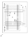
- FIG. 6 is a plan view of a main part of a source short ring TFT forming portion in a frame region of the organic EL display device according to the first embodiment of the present invention.
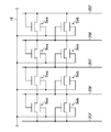
- FIG. 7 is an equivalent circuit diagram showing a source short ring circuit in a frame region of the organic EL display device according to the first embodiment of the present invention.
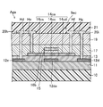
- FIG. 8 is a cross-sectional view of a main part of a source short-ring TFT forming portion in a frame region of the organic EL display device along the line VIII-VIII in FIG.
- FIG. 9 is a plan view of a main part of a gate short ring TFT forming portion in a frame region of the organic EL display device according to the first embodiment of the present invention.
- FIG. 8 is a cross-sectional view of a main part of a source short-ring TFT forming portion in a frame region of the organic EL display device along the line VIII-VIII in FIG.
- FIG. 9 is a plan view of a main
- FIG. 10 is a cross-sectional view of a main part of a gate short-ring TFT forming portion in a frame region of the organic EL display device along the line XX in FIG.
- FIG. 11 is a plan view of a main part of a modified example of the gate short ring TFT forming portion in the frame region of the organic EL display device according to the first embodiment of the present invention.
- FIG. 1 is a plan view showing a schematic configuration of the organic EL display device 50 of the present embodiment.
- FIG. 2 is a plan view of a display area D of the organic EL display device 50.
- FIG. 3 is a cross-sectional view of the display area D of the organic EL display device 50.
- FIG. 4 is an equivalent circuit diagram showing the TFT layer 30 included in the organic EL display device 50.
- FIG. 5 is a cross-sectional view showing the organic EL layer 33 included in the organic EL display device 50.
- FIG. 6 is a plan view of a main part of a source short ring TFT forming portion As in a frame region F of the organic EL display device 50.
- FIG. 7 is an equivalent circuit diagram showing a source short ring circuit in the frame region F of the organic EL display device 50.
- FIG. 8 is a cross-sectional view of a main part of the source short-ring TFT forming portion As along the line VIII-VIII in FIG.
- FIG. 9 is a plan view of a main part of a gate short ring TFT forming portion Aga in a frame region F of the organic EL display device 50.
- FIG. 10 is a cross-sectional view of a main part of the gate short-ring TFT forming portion Aga taken along line XX in FIG.
- the organic EL display device 50 includes, for example, a display area D provided for displaying an image, which is provided in a rectangular shape, and a frame area F provided around the display area D.
- the rectangular display area D is illustrated, but the rectangular shape may be, for example, a shape in which a side is an arc, a shape in which a corner is in an arc, or a part of a side.
- a substantially rectangular shape such as a shape with a notch is also included.
- a plurality of sub-pixels P are arranged in a matrix as shown in FIG.
- a sub-pixel P having a red light-emitting region Lr for displaying red a sub-pixel P having a green light-emitting region Lg for displaying green
- a sub-pixel P having a blue light-emitting region Lb for performing blue display is provided adjacent to each other.
- one pixel is configured by three adjacent sub-pixels P having a red light emitting area Lr, a green light emitting area Lg, and a blue light emitting area Lb.
- a terminal portion T is provided so as to extend in one direction (the horizontal direction in FIG. 1).
- a source short ring TFT forming portion As is provided so as to extend in one direction (horizontal direction in FIG. 1).
- a gate signal control circuit Cg and a light emission control circuit Ce are provided at the right end and the left end in FIG. 1 of the frame region F so as to extend in one direction (vertical direction in FIG. 1).
- a gate short ring TFT forming portion Aga is provided between the display region D and the gate signal control circuit Cg and the light emission control circuit Ce on the left side in FIG.
- a gate short ring TFT forming portion Agb is provided between the display region D and the gate signal control circuit Cg and the light emission control circuit Ce on the right side in FIG.
- a demultiplexer circuit Cs is provided between the terminal portion T and the display area D.
- the gate signal control circuit Cg, the light emission control circuit Ce, and the demultiplexer circuit Cs are provided monolithically on the resin substrate layer 10 described later.
- the configuration in which the gate short ring TFT forming portions Aga and Agb are provided is illustrated, but a configuration in which one of the gate short ring TFT forming portions Aga and Agb is provided may be employed.
- a short ring TFT for a gate line 12d described later is formed in the gate short ring TFT forming portion Aga
- the gate short ring TFT forming portion Agb is formed in the gate short ring TFT forming portion Agb.
- a short ring TFT for the light emission control line 12e described later may be formed.
- the configuration in which the demultiplexer circuit Cs is provided is illustrated, but the present invention can be applied to a configuration in which the demultiplexer circuit Cs is not provided.
- the configuration in which the gate short-ring TFT forming portion Aga (Agb), the gate signal control circuit Cg, and the light emission control circuit Ce are provided on both left and right sides of the display region D is illustrated. (Right) only, the gate short ring TFT forming portion Aga (Agb), the configuration in which the gate signal control circuit Cg and the light emission control circuit Ce are provided, and only the left side (right side) of the display area D, the gate short ring TFT forming portion Aga ( Agb) may be provided, and the gate signal control circuit Cg and the light emission control circuit Ce may be provided only on the right side (left side) of the display area D.
- the organic EL display device 50 includes a resin substrate layer 10 provided as a base substrate, a thin film transistor (TFT) layer 30 provided on the resin substrate layer 10, and a thin film transistor (TFT) layer 30 provided on the resin substrate layer 10.
- the organic EL device includes an organic EL element 35 provided as a light emitting element constituting the display region D, and a sealing film 40 provided to cover the organic EL element 35.
- the resin substrate layer 10 has flexibility and is made of, for example, polyimide resin or the like.
- a polyethylene terephthalate (PET) resin, a polyethylene naphthalate (PEN) resin, a polyether sulfone (PES) resin, an acrylic resin, or the like can be used in addition to the polyimide resin.
- the TFT layer 30 includes a base coat film 11 provided on the resin substrate layer 10, a plurality of first TFTs 9a, a plurality of second TFTs 9b (see FIG. 4) provided on the base coat film 11, and a plurality of The third TFT 9c and the plurality of capacitors 9d, and the first TFT 9a, the second TFT 9b, the third TFT 9c, and the flattening film 21 provided on each capacitor 9d.
- a plurality of gate lines 12d are provided as display wirings so as to extend in parallel in the horizontal direction in the drawing.
- a plurality of light emission control lines 12e are provided as display wirings so as to extend parallel to each other in the horizontal direction in the drawing. Each light emission control line 12e is provided so as to be adjacent to each gate line 12d as shown in FIGS.
- a plurality of source lines 20f are provided as display wirings so as to extend in parallel in the vertical direction in the drawing.
- a plurality of power lines 20g are provided so as to extend parallel to each other in the vertical direction in the figure. Each power supply line 20g is provided adjacent to each source line 20f, as shown in FIGS.
- a first TFT 9a, a second TFT 9b, a third TFT 9c, and a capacitor 9d are provided in each sub-pixel P.
- the base coat film 11 is composed of, for example, a single-layer film or a laminated film of an inorganic insulating film such as silicon nitride, silicon oxide, or silicon oxynitride.
- the first TFT 9a is provided as a write control transistor, and is electrically connected to the corresponding gate line 12d, source line 20f, and second TFT 9b in each sub-pixel P, as shown in FIG.
- the first TFT 9a includes a gate electrode 12a, a first gate insulating film 13, a semiconductor layer 14a, a first interlayer insulating film 17, and a second interlayer insulating film 19 which are sequentially provided on the base coat film 11. , And a source electrode 20a and a drain electrode 20b.
- the gate electrode 12a is provided in an island shape on the base coat film 11, as shown in FIG.
- the first gate insulating film 13 is provided so as to cover the gate electrode 12a, as shown in FIG. As shown in FIG.
- the semiconductor layer 14a is provided on the gate insulating film 13 so as to overlap with the gate electrode 12a, and a channel region overlapping with the gate electrode 12a and a source region arranged with the channel region interposed therebetween. And a drain region.
- the first interlayer insulating film 17 and the second interlayer insulating film 19 are sequentially provided so as to cover the channel region of the semiconductor layer 14a.
- the source electrode 20a and the drain electrode 20b are provided on the second interlayer insulating film 19 so as to be separated from each other. Further, as shown in FIG.
- the source electrode 20a and the drain electrode 20b are connected to the source layer 20a of the semiconductor layer 14a through respective contact holes formed in the laminated film of the first interlayer insulating film 17 and the second interlayer insulating film 19.
- the region is electrically connected to the drain region.
- the first gate insulating film 13, the first interlayer insulating film 17, and the second interlayer insulating film 19 are each formed of a single-layer film or a stacked film of an inorganic insulating film such as silicon nitride, silicon oxide, or silicon oxynitride. ing.
- the semiconductor layer 14a, a semiconductor layer 14b, a semiconductor layer 14ca, and a semiconductor layer 14cb, which will be described later, are made of, for example, an In-Ga-Zn-O-based oxide semiconductor.
- the In—Ga—Zn—O-based semiconductor is a ternary oxide of In (indium), Ga (gallium), and Zn (zinc), and a ratio (composition ratio) of In, Ga, and Zn. Is not particularly limited.
- the In—Ga—Zn—O-based semiconductor may be amorphous or crystalline.
- a crystalline In-Ga-Zn-O-based semiconductor in which the c-axis is oriented substantially perpendicular to the layer surface is preferable.
- Another oxide semiconductor may be included instead of the In-Ga-Zn-O-based semiconductor.
- an In—Sn—Zn—O-based semiconductor eg, In 2 O 3 —SnO 2 —ZnO; InSnZnO
- the In—Sn—Zn—O-based semiconductor is a ternary oxide of In (indium), Sn (tin), and Zn (zinc).
- the oxide semiconductor is an In-Al-Zn-O-based semiconductor, an In-Al-Sn-Zn-O-based semiconductor, a Zn-O-based semiconductor, an In-Zn-O-based semiconductor, or a Zn-Ti-O-based semiconductor.
- Mg x Zn 1-x O magnesium zinc oxide
- Cd x Zn 1-x O cadmium zinc oxide
- Cd x Zn 1-x O cadmium zinc oxide
- an amorphous ZnO to which one or more kinds of impurity elements are added from among Group 1 element, Group 13 element, Group 14 element, Group 15 element, Group 17 element and the like.
- a crystalline state, a polycrystalline state, a microcrystalline state in which an amorphous state and a polycrystalline state are mixed, or a state in which no impurity element is added can be used.
- the second TFT 9b is provided as a driving transistor, and is electrically connected to the corresponding first TFT 9a, power supply line 20g, and third TFT 9c in each sub-pixel P, as shown in FIG.
- the second TFT 9b has substantially the same structure as the first TFT 9a described above and the third TFT 9c described later.
- the third TFT 9c is provided as a light emission control transistor, and is electrically connected to the corresponding second TFT 9b, power supply line 20g, and light emission control line 12e in each sub-pixel P, as shown in FIG.
- the third TFT 9c includes a gate electrode 12b, a first gate insulating film 13, a semiconductor layer 14b, a first interlayer insulating film 17, and a second interlayer insulating film 19, which are sequentially provided on the base coat film 11. , And a source electrode 20c and a drain electrode 20d.
- the gate electrode 12b is provided in an island shape on the base coat film 11, as shown in FIG.
- the first gate insulating film 13 is provided so as to cover the gate electrode 12b.
- the semiconductor layer 14b is provided on the gate insulating film 13 so as to overlap with the gate electrode 12b, and a channel region overlapping with the gate electrode 12b and a source region disposed with the channel region interposed therebetween. And a drain region.
- the first interlayer insulating film 17 and the second interlayer insulating film 19 are sequentially provided so as to cover the channel region of the semiconductor layer 14b.
- the source electrode 20c and the drain electrode 20d are provided on the second interlayer insulating film 19 so as to be separated from each other, as shown in FIG. Further, as shown in FIG.
- the source electrode 20c and the drain electrode 20d are connected to the source electrode of the semiconductor layer 14b through respective contact holes formed in the laminated film of the first interlayer insulating film 17 and the second interlayer insulating film 19.
- the region is electrically connected to the drain region.
- first TFT 9a, the second TFT 9b, and the third TFT 9c of the bottom gate type are illustrated, but the first TFT 9a, the second TFT 9b, and the third TFT 9c may be a top gate type TFT.
- the capacitor 9c is electrically connected to the corresponding first TFT 9a and power supply line 20g in each sub-pixel P.
- the capacitor 9c includes a lower conductive layer 12c formed of the same material on the same layer as the gate electrode 12a and the like, and a first gate insulating layer provided in order to cover the lower conductive layer 12c.
- the semiconductor device includes a film 13, a first interlayer insulating film 17, and an upper conductive layer 18 provided on the first interlayer insulating film 17 so as to overlap the lower conductive layer 12 c.
- the upper conductive layer 18 is electrically connected to a power line 20g as shown in FIG.
- the flattening film 21 is made of, for example, an organic resin material such as a polyimide resin.
- the organic EL element 35 includes a plurality of first electrodes 31, an edge cover 32, a plurality of organic EL layers 33, and a second electrode 34 which are sequentially provided on the planarizing film 21.
- the plurality of first electrodes 31 are provided in a matrix on the flattening film 21 so as to correspond to the plurality of sub-pixels P, as shown in FIG. Further, as shown in FIG. 3, each first electrode 31 is electrically connected to a drain electrode 20d of each third TFT 9c via a contact hole formed in the planarizing film 21.
- the first electrode 31 has a function of injecting holes (holes) into the organic EL layer 33. Further, the first electrode 31 is more preferably formed of a material having a large work function in order to improve the efficiency of injecting holes into the organic EL layer 33.
- the material forming the first electrode 31 for example, silver (Ag), aluminum (Al), vanadium (V), cobalt (Co), nickel (Ni), tungsten (W), gold (Au) , Titanium (Ti), ruthenium (Ru), manganese (Mn), indium (In), ytterbium (Yb), lithium fluoride (LiF), platinum (Pt), palladium (Pd), molybdenum (Mo), iridium ( Metal materials such as Ir) and tin (Sn). Further, the material forming the first electrode 31 may be an alloy such as astatine (At) / astatin oxide (AtO 2 ).
- the material forming the first electrode 31 is, for example, a conductive oxide such as tin oxide (SnO), zinc oxide (ZnO), indium tin oxide (ITO), and indium zinc oxide (IZO). There may be. Further, the first electrode 31 may be formed by stacking a plurality of layers made of the above materials. Note that examples of the compound material having a large work function include indium tin oxide (ITO) and indium zinc oxide (IZO).
- the edge cover 32 is provided in a lattice shape so as to cover the peripheral portion of each first electrode 31.
- a material forming the edge cover 32 include a positive photosensitive resin such as a polyimide resin, an acrylic resin, a polysiloxane resin, and a novolak resin.
- each of the organic EL layers 33 is disposed on each first electrode 31 as shown in FIG. 3 and provided in a matrix so as to correspond to the plurality of sub-pixels P.
- each of the organic EL layers 33 includes a hole injection layer 1, a hole transport layer 2, a light emitting layer 3, an electron transport layer 4, and an electron injection layer which are sequentially provided on the first electrode 31. It has a layer 5.
- the hole injection layer 1 is also called an anode buffer layer, and has a function of making the energy levels of the first electrode 31 and the organic EL layer 33 close to each other and improving the efficiency of hole injection from the first electrode 31 to the organic EL layer 33.
- a material constituting the hole injection layer for example, a triazole derivative, an oxadiazole derivative, an imidazole derivative, a polyarylalkane derivative, a pyrazoline derivative, a phenylenediamine derivative, an oxazole derivative, a styrylanthracene derivative, a fluorenone derivative, Hydrazone derivatives, stilbene derivatives and the like can be mentioned.
- the hole transport layer 2 has a function of improving the efficiency of transporting holes from the first electrode 31 to the organic EL layer 33.
- a material constituting the hole transport layer 2 for example, a porphyrin derivative, an aromatic tertiary amine compound, a styrylamine derivative, polyvinyl carbazole, poly-p-phenylene vinylene, polysilane, a triazole derivative, oxadiazole Derivatives, imidazole derivatives, polyarylalkane derivatives, pyrazoline derivatives, pyrazolone derivatives, phenylenediamine derivatives, arylamine derivatives, amine-substituted chalcone derivatives, oxazole derivatives, styrylanthracene derivatives, fluorenone derivatives, hydrazone derivatives, stilbene derivatives, hydrogenated amorphous silicon, Examples include hydrogenated amorphous silicon carbide, zinc sulfide, and zinc selenide.
- the light emitting layer 3 is formed of a material having high luminous efficiency.
- the material constituting the light emitting layer 3 include a metal oxinoid compound [8-hydroxyquinoline metal complex], a naphthalene derivative, an anthracene derivative, a diphenylethylene derivative, a vinylacetone derivative, a triphenylamine derivative, a butadiene derivative, and a coumarin derivative.
- the electron transport layer 4 has a function of efficiently moving electrons to the light emitting layer 3.
- a material constituting the electron transport layer 4 for example, as an organic compound, an oxadiazole derivative, a triazole derivative, a benzoquinone derivative, a naphthoquinone derivative, an anthraquinone derivative, a tetracyanoanthraquinodimethane derivative, a diphenoquinone derivative, or a fluorenone derivative , Silole derivatives, metal oxinoid compounds and the like.
- the electron injection layer 5 has a function of making the energy levels of the second electrode 34 and the organic EL layer 33 close to each other, and improving the efficiency with which electrons are injected from the second electrode 34 into the organic EL layer 33.
- the drive voltage of the organic EL element 35 can be reduced. Note that the electron injection layer 5 is also called a cathode buffer layer.
- lithium fluoride LiF
- magnesium fluoride MgF 2
- calcium fluoride CaF 2
- strontium fluoride SrF 2
- barium fluoride examples thereof include an inorganic alkali compound such as (BaF 2 ), aluminum oxide (Al 2 O 3 ), and strontium oxide (SrO).
- the second electrode 34 is provided so as to cover each of the organic EL layers 33 and the edge cover 32, as shown in FIG.
- the second electrode 34 has a function of injecting electrons into the organic EL layer 33.
- the second electrode 34 is more preferably made of a material having a small work function in order to improve the efficiency of injecting electrons into the organic EL layer 33.
- the second electrode 34 for example, silver (Ag), aluminum (Al), vanadium (V), cobalt (Co), nickel (Ni), tungsten (W), gold (Au) , Calcium (Ca), titanium (Ti), yttrium (Y), sodium (Na), ruthenium (Ru), manganese (Mn), indium (In), magnesium (Mg), lithium (Li), ytterbium (Yb) , Lithium fluoride (LiF) and the like.
- the second electrode 34 is made of, for example, magnesium (Mg) / copper (Cu), magnesium (Mg) / silver (Ag), sodium (Na) / potassium (K), astatine (At) / astatin oxide (AtO 2). ), Lithium (Li) / aluminum (Al), lithium (Li) / calcium (Ca) / aluminum (Al), and lithium fluoride (LiF) / calcium (Ca) / aluminum (Al). You may. Further, the second electrode 34 may be formed of a conductive oxide such as tin oxide (SnO), zinc oxide (ZnO), indium tin oxide (ITO), and indium zinc oxide (IZO). .
- a conductive oxide such as tin oxide (SnO), zinc oxide (ZnO), indium tin oxide (ITO), and indium zinc oxide (IZO).
- the second electrode 34 may be formed by laminating a plurality of layers made of the above materials.
- the material having a small work function include magnesium (Mg), lithium (Li), lithium fluoride (LiF), magnesium (Mg) / copper (Cu), magnesium (Mg) / silver (Ag), and sodium (Mg).
- (Na) / potassium (K) lithium (Li) / aluminum (Al), lithium (Li) / calcium (Ca) / aluminum (Al), lithium fluoride (LiF) / calcium (Ca) / aluminum (Al) And the like.
- the sealing film 40 includes a first inorganic film 36 provided to cover the second electrode 34, an organic film 37 provided on the first inorganic film 36, and an organic film 37.
- a second inorganic film provided so as to cover the film 37, and has a function of protecting the organic EL layer 33 from moisture, oxygen, and the like.
- the first inorganic film 36 and the second inorganic film 38 are made of, for example, silicon nitride (Si 2 N 3 ) such as silicon oxide (SiO 2 ), aluminum oxide (Al 2 O 3 ), or trisilicon tetranitride (Si 3 N 4 ).
- the organic film 37 is made of, for example, an organic material such as an acrylic resin, a polyurea resin, a parylene resin, a polyimide resin, and a polyamide resin.
- one end (upper side in the drawing) of the plurality of source lines 20f is connected to the source short ring TFT forming portion As in the frame region F as shown in FIGS. And a plurality of lead wirings electrically connected to the plurality of source lines 20f.
- a first short ring TFT 9ea and a second short ring TFT 9eb are arranged between a pair of adjacent source lines 20f.
- the configuration in which the two short ring TFTs 9ea and 9eb are provided between a pair of adjacent source lines 20f is exemplified.
- the short ring TFT is provided between the pair of adjacent source lines 20f. More than one may be arranged.
- the first short ring TFT 9ea is provided on the semiconductor layer 14ca, the first gate electrode 12fa provided on the resin substrate layer 10 side of the semiconductor layer 14ca, and provided on the organic EL element 35 side of the semiconductor layer 14ca.
- a second gate insulating film 15 see FIG. 8
- the semiconductor layer 14ca has a channel region 14cc (see FIG. 8) provided so as to overlap the first gate electrode 12fa and the second gate electrode 16a, and a source region 14cs (see FIG.
- a pair of adjacent ones is formed in the source region 14cs of the semiconductor layer 14ca via a contact hole Ha formed in a stacked film of the first interlayer insulating film 17 and the second interlayer insulating film 19.
- One of the source lines 20f (left side in the figure) is electrically connected (see FIG. 8).
- a pair of adjacent ones is formed in the drain region 14cd of the semiconductor layer 14ca via a contact hole Hb formed in a stacked film of the first interlayer insulating film 17 and the second interlayer insulating film 19.
- the other (right side in the figure) of the source line 20f is electrically connected (see FIG. 8).
- the first gate electrode 12fa is adjacent via a contact hole Hc formed in a stacked film of the first gate insulating film 13, the first interlayer insulating film 17, and the second interlayer insulating film 19.
- This is a short-circuit gate electrode electrically connected to the other (the right side in the figure) of the pair of source lines 20f that match.
- the second gate electrode 16a is a threshold control gate electrode electrically connected to a threshold control wiring 16 provided in a frame shape in the frame region F.
- the second gate electrode 16a is a branch wiring in which the threshold control wiring 16 branches toward the first short ring TFT 9ea and the second short ring TFT 9eb.
- the source region 14cs and the drain region 14cd merely distinguish between the two regions for the sake of convenience. And the drain region 14cd may be replaced with each other.
- the second short ring TFT 9eb includes a semiconductor layer 14cb, a first gate electrode 12fb provided on the resin substrate layer 10 side of the semiconductor layer 14cb, and an organic EL element 35 of the semiconductor layer 14cb.
- the second gate electrode 16a provided on the side, the first gate insulating film 13 provided between the semiconductor layer 14cb and the first gate electrode 12fb, and the second gate electrode 16a provided between the semiconductor layer 14cb and the second gate electrode 16a And a second gate insulating film 15.
- the semiconductor layer 14cb includes a channel region 14cc provided so as to overlap the first gate electrode 12fb and the second gate electrode 16a, a source region 14cs provided across the channel region 14cc, and And a drain region 14cd.
- the source region 14cs of the semiconductor layer 14cb is adjacent to the source region 14cs via a contact hole Ha formed in a stacked film of the first interlayer insulating film 17 and the second interlayer insulating film 19.
- One (left side in the figure) of a pair of matching source lines 20f is electrically connected.
- the drain region 14cd of the semiconductor layer 14cb is adjacent to the drain region 14cd via a contact hole Hb formed in the stacked film of the first interlayer insulating film 17 and the second interlayer insulating film 19.
- the other (right side in the figure) of the pair of matched source lines 20f is electrically connected.
- the first gate electrode 12fb is formed via a contact hole Hc formed in a stacked film of the first gate insulating film 13, the first interlayer insulating film 17, and the second interlayer insulating film 19, It is a short-circuit gate electrode electrically connected to one of the adjacent pair of source lines 20f (left side in the figure).
- the second gate electrode 16a is a threshold control gate electrode electrically connected to a threshold control wiring 16 provided in a frame shape in the frame region F. As shown in FIG. 6, the second gate electrode 16a is provided so as to be shared by the first short ring TFT 9ea and the second short ring TFT 9eb.
- the other (lower side in the figure) end of the plurality of source lines 20f is drawn out to the demultiplexer circuit Cs in the frame region F and then adjacent to the other end as shown in FIG. It is drawn out to the terminal part T for every two fittings.
- the demultiplexer circuit Cs which is provided for each two adjacent source lines 20f and distributes one data signal to two is exemplified.
- the demultiplexer circuit Cs includes three adjacent source lines 20f. One data signal may be allocated to every 20f and divided into three.
- both ends of the plurality of power lines 20g are drawn out to the frame region F, and are connected to a frame wiring (not shown) provided in the frame region F and receiving a high power supply voltage (ELVDD). It is electrically connected.
- a frame wiring not shown
- ELVDD high power supply voltage
- both end portions of the plurality of gate lines 12d are drawn out to the gate short ring TFT forming portion Aga and the gate short ring TFT forming portion Agb in the frame region F as shown in FIG.
- both end portions of the plurality of light emission control lines 12e are led out to the gate short ring TFT forming portion Aga and the gate short ring TFT forming portion Agb in the frame region F, as shown in FIG.
- the gate short ring circuit has the same structure as the source short ring circuit (see FIG.
- the first short ring TFT 9ec and the light emitting control line 12e are provided between the adjacent gate line 12d and light emission control line 12e.
- the second short ring TFT 9ed is arranged.
- the configuration in which the two short ring TFTs 9ec and 9ed are provided between the adjacent gate line 12d and the light emission control line 12e is exemplified.
- the short ring TFT is provided with the adjacent gate line 12d and the light emission control line 12e. Three or more lines may be arranged between the lines 12e.
- the first short ring TFT 9ec includes a semiconductor layer 14ca, a first gate electrode 12da provided on the resin substrate layer 10 side of the semiconductor layer 14ca, and an organic EL element 35 of the semiconductor layer 14ca.
- the second gate electrode 16b provided on the side, the first gate insulating film 13 provided between the semiconductor layer 14ca and the first gate electrode 12da, and the second gate electrode 16b provided between the semiconductor layer 14ca and the second gate electrode 16b And a second gate insulating film 15.
- the semiconductor layer 14ca includes a channel region 14cc provided so as to overlap the first gate electrode 12da and the second gate electrode 16b, and a source region 14cs provided across the channel region 14cc.
- a drain region 14cd In the source region 14cs of the semiconductor layer 14ca, as shown in FIGS. 9 and 10, a contact hole He and a source contact layer 20h formed in a stacked film of the first interlayer insulating film 17 and the second interlayer insulating film 19 are provided.
- the light emission control line 12e is electrically connected through a contact hole Hd formed in a stacked film of the first gate insulating film 13, the first interlayer insulating film 17, and the second interlayer insulating film 19.
- the contact hole Hf and the source contact layer 20i formed in the stacked film of the first interlayer insulating film 17 and the second interlayer insulating film 19 are formed.
- the gate line 12d is electrically connected through a contact hole Hg formed in a stacked film of the first gate insulating film 13, the first interlayer insulating film 17, and the second interlayer insulating film 19. Further, as shown in FIG. 9, the first gate electrode 12da is a portion where the gate line 12d protrudes laterally in an L shape, and is a short-circuit gate electrode electrically connected to the gate line 12d.
- the second gate electrode 16b is a threshold control gate electrode electrically connected to the threshold control wiring 16 provided in a frame shape in the frame region F.
- the second gate electrode 16b is a branch wiring in which the threshold control wiring 16 branches toward the first short ring TFT 9ec and the second short ring TFT 9ed.
- the second short ring TFT 9ed is provided on the semiconductor layer 14cb, the first gate electrode 12ea provided on the resin substrate layer 10 side of the semiconductor layer 14cb, and provided on the organic EL element 35 side of the semiconductor layer 14cb.
- a second gate insulating film 15 see FIG. 10
- the semiconductor layer 14cb includes a channel region 14cc (see FIG.
- a source region 14cs (see FIG. 10) provided across the channel region 14cc. 10) and a drain region 14cd (see FIG. 10).
- a contact hole He formed in a stacked film of the first interlayer insulating film 17 and the second interlayer insulating film 19
- a source contact layer 20h a source contact layer 20h
- the light emission control line 12e is electrically connected through a contact hole Hd formed in a stacked film of the first gate insulating film 13, the first interlayer insulating film 17, and the second interlayer insulating film 19.
- the gate line 12d is electrically connected through a contact hole Hg formed in a stacked film of the first gate insulating film 13, the first interlayer insulating film 17, and the second interlayer insulating film 19.
- the first gate electrode 12ea is a portion where the light emission control line 12e protrudes laterally in an L-shape, and is a short-circuit gate electrode electrically connected to the light emission control line 12e. .
- the second gate electrode 16b is a threshold control gate electrode electrically connected to the threshold control wiring 16 provided in a frame shape in the frame region F. Note that, as shown in FIG. 9, the second gate electrode 16b is provided so as to be shared by the first short ring TFT 9ec and the second short ring TFT 9ed.
- the first short ring TFTs 9ea and 9ec and the second short ring TFTs 9eb and 9ed are n-type transistors, and a negative voltage such as a low power supply voltage (ELDSS) is input to the threshold control wiring 16, for example.
- EDSS low power supply voltage
- the degree of threshold control depends on the ratio between the capacitance between the short-circuit gate electrode and the semiconductor layer and the capacitance between the threshold control gate electrode and the semiconductor layer. That is, as the capacitance between the threshold control gate electrode and the semiconductor layer is larger than the capacitance between the short gate electrode and the semiconductor layer, the short ring TFT can be turned off with a smaller threshold control voltage.
- the thickness of the first gate insulating film 13 between the short-circuit gate electrodes (12fa, 12fb, 12da, 12ea) and the semiconductor layers (14ca, 14cb) is set to a threshold control gate electrode (16a, 9B
- the thickness of the second gate insulating film 15 between the semiconductor layers (14ca, 14cb) and the channel direction of the threshold control gate electrodes (16a, 16b) (horizontal direction in FIG. 6, FIG.
- the length in the middle (vertical direction) may be longer than the length of the short-circuit gate electrodes (12fa, 12fb, 12da, 12ea) in the channel direction.
- FIG. 11 is a plan view of a main part of a modified example of the gate short ring TFT forming portion Aga.
- the contact holes for electrically connecting the semiconductor layer 14d to the gate line 12d and the light emission control line 12e need only be the contact holes Hi and Hh. Therefore, the semiconductor layer 14d and the gate line 12d and the light emission control line 12e can be conducted with a small area, and the pitch between wirings can be narrowed.
- This modification can also be applied to a short ring TFT between adjacent source lines 20f.
- the wiring structure in which the display wiring is directly drawn out to the frame region F is illustrated, but the display wiring may be drawn out by switching to another conductive layer in the frame region F.
- the configuration in which the source short ring TFT forming portion As is provided on the side opposite to one side of the frame region F having the terminal portion T is illustrated, but the source short ring TFT forming portion As is provided with a display. It may be provided between the region D and the demultiplexer circuit Cs. In this case, it is necessary to form the short ring TFTs 9ea and 9eb while avoiding the high power supply voltage main wiring (not shown) orthogonal to the plurality of power supply lines 20g. And the opposite side is preferred. Since the plurality of power supply lines 20g are electrically connected to the high power supply voltage main wiring, it is not necessary to take countermeasures against static electricity by the short ring TFT.
- a gate signal is input to the first TFT 9a via the gate line 12d, so that the first TFT 9a is turned on, and the gate of the second TFT 9b is connected via the source line 20f.
- a data signal is written to the electrode and the capacitor 9d and a light emission control signal is input to the third TFT 9c via the light emission control line 12e, the third TFT 9c is turned on, and a current corresponding to the gate voltage of the second TFT 9b is supplied to the power supply line.
- 20 g is supplied to the organic EL layer 33, the light emitting layer 3 of the organic EL layer 33 emits light, and an image is displayed.
- the gate voltage of the second TFT 9b is held by the capacitor 9d, so that the light emitting layer 3 emits light until a gate signal of the next frame is input. It is maintained at each sub-pixel P.
- the threshold voltage of the first short ring TFTs 9ea and 9ec and the threshold value of the second short ring TFTs 9eb and 9ed are set to the magnitude of the negative voltage by inputting a negative voltage to the threshold control wiring 16.
- the first short ring TFTs 9ea and 9ec and the second short ring TFTs 9eb and 9ed are turned off, so that the display signal does not interfere.
- the method for manufacturing the organic EL display device 50 of the present embodiment includes a TFT layer forming step, an organic EL element forming step, and a sealing film forming step.
- ⁇ TFT layer forming step> First, for example, a silicon oxide (SiOx), a silicon nitride (SiNx), and a silicon oxynitride (SiOxNy; x> y) are formed on a resin substrate layer 10 formed on a glass substrate, for example, by a plasma CVD (Chemical Vapor Deposition) method. ), An inorganic insulating film (thickness of about 50 nm) such as silicon nitride oxide (SiNxOy; x> y) is formed, and the base coat film 11 is formed.
- SiOx silicon oxide
- SiNxOy silicon nitride oxide
- x> y silicon oxynitride
- an aluminum film about 350 nm in thickness
- a molybdenum nitride film about 50 nm in thickness
- the gate electrodes 12a and 12b, the lower conductive layer 12c, the gate line 12d, the emission control line 12e, and the first gate electrodes 12fa, 12fb, and 12ea are subjected to photolithography, etching, and resist stripping. And 12da are formed.
- an inorganic insulating film such as a silicon oxide film (SiOx) is formed on the entire substrate on which the gate electrode 12a and the like are formed by a plasma CVD method.
- an oxide semiconductor film (for example, about 30 nm to 100 nm in thickness) of, for example, InGaZnO 4 is formed over the entire substrate on which the gate insulating film 13 is formed by a sputtering method.
- the semiconductor layers 14a, 14b, 14ca, and 14cb are formed by performing photolithography, etching, and resist stripping.
- an inorganic insulating film (about 150 nm thick) such as a silicon oxide film is formed on the entire substrate on which the semiconductor layer 14a and the like are formed by, for example, a plasma CVD method, and then, for example, an aluminum film is formed by a sputtering method. (Thickness: about 350 nm) and a molybdenum nitride film (thickness: about 50 nm) are formed in this order, and a photolithography process, an etching process, and a resist stripping process are performed on the metal laminated film and the inorganic insulating film. , A second gate insulating film 15, a threshold control line 16, and second gate electrodes 16a and 16b.
- the entire substrate on which the threshold control lines 16 and the like are formed is subjected to plasma processing such as hydrogen plasma processing or helium plasma processing, so that the semiconductor layers 14a, 14b, 14ca and 14cb have the channel region 14cc and the source region. 14cs and the drain region 14cd are respectively formed.
- plasma processing such as hydrogen plasma processing or helium plasma processing
- a silicon nitride film (about 100 nm thick) and a silicon oxide film (about 100 nm thick) are formed on the entire substrate on which the channel region 14 cc and the like are formed by, for example, a plasma CVD method. Forming an aluminum film (about 350 nm in thickness) and a molybdenum nitride film (about 50 nm in thickness) in that order, and then performing photolithography, etching, and resist stripping on the metal laminated film. Thereby, the upper conductive layer 18 is formed.
- a silicon nitride film (about 100 nm in thickness) and a silicon oxide film (about 100 nm in thickness) are formed on the entire substrate on which the upper conductive layer 18 is formed, for example, by a plasma CVD method.
- Photolithography, etching, and resist stripping are performed on the inorganic insulating film to form contact holes Ha to Hg, and the first interlayer insulating film 17 and the second interlayer insulating film 17 having the contact holes Ha to Hg are formed.
- An insulating film 19 is formed.
- a titanium film (about 30 nm in thickness), an aluminum film (about 300 nm in thickness) and a titanium film (about 50 nm in thickness) are sequentially formed on the entire substrate on which the second interlayer insulating film 19 is formed, for example, by a sputtering method.
- the metal laminated film is subjected to a photolithography process, an etching process, and a resist stripping process to form a source line 20f, a power supply line 20g, and source contact layers 20h and 20i.
- a polyimide photosensitive resin film (about 2 ⁇ m thick) is applied to the entire substrate on which the source lines 20f and the like are formed by, for example, a spin coating method or a slit coating method.
- the flattening film 21 is formed, and the TFT layer 30 is formed.
- ⁇ Organic EL element forming step> The first electrode 31, the edge cover 32, the organic EL layer 33 (the hole injection layer 1, the hole transport layer) are formed on the flattening film 21 of the TFT layer 30 formed in the above-described TFT layer forming step by using a known method.
- the layer 2, the light emitting layer 3, the electron transport layer 4, the electron injection layer 5) and the second electrode 34 are formed to form an organic EL element 35.
- ⁇ Sealing film forming step> an inorganic insulating film such as a silicon nitride film, a silicon oxide film, or a silicon oxynitride film is formed on a surface of a substrate on which the organic EL element 35 formed in the above-described organic EL element forming step is formed by plasma using a mask.
- a first inorganic film 36 is formed by a CVD method.
- an organic resin material such as an acrylic resin is formed on the surface of the substrate on which the first inorganic film 36 is formed, for example, by an ink-jet method to form an organic film 37.
- an inorganic insulating film such as a silicon nitride film, a silicon oxide film, a silicon oxynitride film, or the like is formed on the substrate on which the organic film 37 is formed by a plasma CVD method using a mask.
- the sealing film 40 is formed by forming the inorganic film 38.
- the organic EL display device 50 of the present embodiment can be manufactured.
- the first gate electrode 12fa of the first short ring TFT 9ea and the first gate electrode 12fb of the second short ring TFT 9eb are floating electrodes, if an excessive voltage is applied to the source line 20f by static electricity, the The first short ring TFT 9ea or the second short ring TFT 9eb is turned on, and an excessive voltage flows to the adjacent source line 20f sequentially, so that an excessive voltage is discharged.
- first gate electrode 12da of the first short ring TFT 9ec and the first gate electrode 12ea of the second short ring TFT 9ed are floating electrodes, an excessive voltage is applied to the gate line 12d or the light emission control line 12e by static electricity. Then, the first short-ring TFT 9ec or the second short-ring TFT 9ed is turned on, and an excessive voltage sequentially flows to the adjacent light emission control line 12e or the gate line 12d, so that an excessive voltage is discharged.
- the first short ring TFT 9ea provided between the pair of adjacent source lines 20f includes the semiconductor layer 14ca and the resin substrate of the semiconductor layer 14ca.
- one source line 20f is electrically connected to the source region 14cs of the semiconductor layer 14ca
- the other source line 20f is electrically connected to the drain region 14cd of the semiconductor layer 14ca
- the first gate electrode 12fa is The drain electrode 14cd of the layer 14ca is electrically connected
- the second gate electrode 16a is electrically connected to the threshold control wiring 16.
- a second short ring TFT 9eb provided between a pair of adjacent source lines 20f is provided between the semiconductor layer 14cb and the resin substrate layer 10 side of the semiconductor layer 14cb via the first gate insulating film 13. It has one gate electrode 12fb and a second gate electrode 16a provided on the organic EL element 35 side of the semiconductor layer 14cb via the second gate insulating film 15.
- one source line 20f is electrically connected to the source region 14cs of the semiconductor layer 14cb
- the other source line 20f is electrically connected to the drain region 14cd of the semiconductor layer 14cb
- the first gate electrode 12fb is The source region 14cs of the layer 14cb is electrically connected
- the second gate electrode 16a is electrically connected to the threshold control wiring 16.
- the first short ring TFT 9ea or the second short ring TFT 9eb is turned on, and the excessive voltage is sequentially applied to the adjacent source line 20f. , An excessive voltage is discharged.
- a threshold voltage of the first short-ring TFT 9ea and the second short-ring TFT 9eb shifts to a positive value when a negative voltage is input to the threshold control wiring 16, so that the first short-ring TFT 9ea
- the second short ring TFT 9eb is turned off, and the display signal does not interfere with each other.
- the first short ring TFT 9ea and the second short ring TFT 9eb for countermeasures against static electricity can be kept incorporated in the product, so that a short ring that does not need to be separated and removed can be provided in the organic EL display device 50. .
- the first short ring TFT 9ec provided between the adjacent gate line 12d and the emission control line 12e includes the semiconductor layer 14ca and the resin substrate layer of the semiconductor layer 14ca.
- the emission control line 12e is electrically connected to the source region 14cs of the semiconductor layer 14ca
- the gate line 12d is electrically connected to the drain region 14cd of the semiconductor layer 14ca
- the first gate electrode 12da is connected to the semiconductor layer 14ca.
- the second gate electrode 16 b is electrically connected to the drain region 14 cd and the threshold control wiring 16.
- a second short ring TFT 9ed provided between the adjacent gate line 12d and the emission control line 12e is provided on the semiconductor layer 14cb and the resin substrate layer 10 side of the semiconductor layer 14cb via the first gate insulating film 13.
- a second gate electrode 16b provided on the organic EL element 35 side of the semiconductor layer 14cb via the second gate insulating film 15.
- the emission control line 12e is electrically connected to the source region 14cs of the semiconductor layer 14cb
- the gate line 12d is electrically connected to the drain region 14cd of the semiconductor layer 14cb
- the first gate electrode 12ea is connected to the semiconductor layer 14cb.
- the second gate electrode 16 b is electrically connected to the source region 14 cs and the threshold control wiring 16. Therefore, when an excessive voltage is applied to the gate line 12d or the light emission control line 12e due to static electricity during the manufacturing process, the first short ring TFT 9ec or the second short ring TFT 9ed is turned on, and the excessive voltage is applied to the next light emission. Excessive voltage is discharged by flowing sequentially to the control line 12e or the gate line 12d.
- the threshold voltage of the first short-ring TFT 9ec and the threshold value of the second short-ring TFT 9ed are shifted to a positive value by inputting a negative voltage to the threshold control wiring 16, so that the first short-ring TFT 9ec
- the second short ring TFT 9ed is turned off, and the display signal does not interfere. Accordingly, the first short ring TFT 9ec and the second short ring TFT 9ed for countermeasures against static electricity can be kept incorporated in the product, so that a short ring that does not need to be separated and removed can be provided in the organic EL display device 50. .
- the organic EL display device 50 of the present embodiment since the end surface of the lead-out wiring is not exposed at the divided plane divided into panel units, an overvoltage due to static electricity or moisture due to moisture is applied through the end surface of the lead-out wiring. It is possible to suppress the deterioration of the wiring and the progress of the deterioration in the display area.
- the first short ring TFTs 9ea and 9ec and the second short ring TFTs 9ec and 9ed remain even after being divided into panel units. Later electrostatic damage can be suppressed. In particular, since the flexible organic EL display device 50 sticks or peels off the laminate film, the electrostatic breakdown at that time can be effectively suppressed.
- the organic EL display device 50 of the present embodiment since the first gate insulating film 13 is provided thicker than the second gate insulating film 15, the first short ring TFTs 9ea and 9ec and the second short ring The TFTs 9eb and 9ed can be turned off with a small threshold control voltage.
- the organic EL display device 50 provided with an n-type TFT including a semiconductor layer made of an oxide semiconductor is illustrated.
- a p-type organic light-emitting device having a semiconductor made of low-temperature polysilicon is used.
- An organic EL display device provided with a TFT may be used.
- the first short-ring TFTs 9ea and 9ec and the second short-ring TFT 9eb are input to the threshold control wiring 16 by inputting, for example, a high power supply voltage (ELVDD) as a positive voltage.
- ELVDD high power supply voltage
- the organic EL layer having a five-layered structure of the hole injection layer, the hole transport layer, the light emitting layer, the electron transport layer, and the electron injection layer is exemplified. It may have a three-layer structure of a layer / hole transport layer, a light emitting layer, and an electron transport layer / electron injection layer.
- the organic EL display device in which the first electrode is used as an anode and the second electrode is used as a cathode is exemplified.
- the present invention inverts the stacked structure of the organic EL layer and uses the first electrode as a cathode. It can be applied to an organic EL display device using the second electrode as an anode. In this case, a low power supply voltage is input to the power supply line.
- the organic EL display device in which the light emission control line is provided as the display wiring has been exemplified. It can also be applied to devices.
- the organic EL display device in which the first gate electrode is a short-circuit gate electrode and the second gate electrode is a threshold control gate electrode is exemplified. It is also applicable to an organic EL display device in which the first gate electrode is a threshold control gate electrode.
- the organic EL display device in which the electrode of the TFT connected to the first electrode is used as the drain electrode is exemplified.
- the present invention relates to the case where the electrode of the TFT connected to the first electrode is used as the source electrode. It can also be applied to an organic EL display device called.
- the organic EL display device has been described as an example of the display device, but the present invention can be applied to a display device having a plurality of light emitting elements driven by current.
- the present invention can be applied to a display device including a QLED (Quantum-dot-light-emitting-diode) which is a light-emitting element using a quantum dot-containing layer.
- QLED Quantum-dot-light-emitting-diode
- the present invention is useful for a flexible display device.
- Gate signal control circuits 9ea, 9ec First short ring TFT 9eb, 9ed 2nd short ring TFT 10 Resin substrate layer (base substrate) 12d gate line (display wiring, lead wiring) 12da first gate electrode (short-circuit gate electrode) 12fa, 12fb First gate electrode (short-circuit gate electrode) 12e Light emission control line (display wiring, lead wiring) 12ea First gate electrode (short-circuit gate electrode) 13 First gate insulating films 14ca, 14cb Semiconductor layer 14cc Channel region 14cd Drain region 14cs Source region 15 Second gate insulating film 16 Threshold control wiring 16a Second gate electrode (threshold control gate electrode) 20f source line (display wiring, lead wiring) 35 Organic EL device (light emitting device) 50 Organic EL display
Landscapes
- Engineering & Computer Science (AREA)
- Physics & Mathematics (AREA)
- General Physics & Mathematics (AREA)
- Theoretical Computer Science (AREA)
- Microelectronics & Electronic Packaging (AREA)
- Computer Hardware Design (AREA)
- Electroluminescent Light Sources (AREA)
- Devices For Indicating Variable Information By Combining Individual Elements (AREA)
Abstract
ショートリングTFT(9ea)が、半導体層(14ca)と、半導体層(14ca)に第1ゲート絶縁膜(13)を介して設けられた第1ゲート電極(12fa)と、半導体層(14ca)に第2ゲート絶縁膜(15)を介して設けられた第2ゲート電極(16a)とを備え、半導体層(14ca)のソース領域に一方の引出配線(20f)が接続され、半導体層(14ca)のドレイン領域に他方の引出配線(20f)が接続され、第1ゲート電極(12fa)が半導体層(14ca)のソース領域又はドレイン領域に接続され、第2ゲート電極(16a)が閾値制御配線(16)に接続されている。
Description
本発明は、表示装置に関するものである。
近年、液晶表示装置に代わる表示装置として、有機EL(electroluminescence)素子を用いた自発光型の有機EL表示装置が注目されている。ここで、有機EL表示装置では、画像表示を行う表示領域に、例えば、ゲート線、ソース線、電源線等の複数の表示用配線が設けられている。そして、複数の表示用配線は、表示領域の周囲の額縁領域にそれぞれ引き出され、それらの引き出された複数の引出配線は、静電気対策として額縁領域に設けられたショートリングに電気的に接続されていることが多い。ここで、ショートリングとは、配線間に電気的な抵抗を設けて、静電気を放電させる構造を指す。
例えば、特許文献1には、ゲート線及びソース線の引出配線がショートリングに電気的に接続され、引出配線の横に電極が設けられ、ショートリングの切断除去前は、電極と引出線とが電気的に独立し、ショートリングの切断除去後は、電極と引出配線とが電気的に接続されるアレイ基板が開示されている。
ところで、上記特許文献1のように、ショートリングに電気的に接続された引出配線は、ショートリングを分断除去した後に、分断面に端面が露出するので、引出配線の端面を介して、静電気による過度な電圧が印加されたり、水分による配線が劣化し、その劣化が表示領域内に進行したりするおそれがある。
本発明は、かかる点に鑑みてなされたものであり、その目的とするところは、分断除去不要なショートリングを表示装置内に設けることにある。
上記目的を達成するために、本発明に係る表示装置は、画像表示を行う表示領域、及び該表示領域の周囲に額縁領域が規定されたベース基板と、上記ベース基板の一方の表面側に設けられ、上記表示領域を構成する発光素子と、上記ベース基板及び上記発光素子の間において、上記表示領域に設けられた複数の表示用配線と、上記ベース基板及び上記発光素子の間において、上記額縁領域に設けられ、上記複数の表示用配線にそれぞれ電気的に接続された複数の引出配線とを備え、上記複数の引出配線における隣り合う一対の引出配線の間にショートリングTFTが配置された表示装置であって、上記ショートリングTFTは、チャネル領域、並びに該チャネル領域を挟んで配置されたソース領域及びドレイン領域を有する半導体層と、該半導体層の上記ベース基板側に上記チャネル領域と重なるように設けられた第1ゲート電極と、該半導体層の上記発光素子側に上記チャネル領域と重なるように設けられた第2ゲート電極と、上記半導体層及び上記第1ゲート電極の間に設けられた第1ゲート絶縁膜と、上記半導体層及び上記第2ゲート電極の間に設けられた第2ゲート絶縁膜とを備え、上記ソース領域には、上記隣り合う一対の引出配線の一方が電気的に接続され、上記ドレイン領域には、上記隣り合う一対の引出配線の他方が電気的に接続され、上記第1ゲート電極及び上記第2ゲート電極の一方は、上記ソース領域又は上記ドレイン領域に電気的に接続された短絡ゲート電極であり、上記第1ゲート電極及び上記第2ゲート電極の他方は、上記額縁領域に設けられた閾値制御配線に電気的に接続された閾値制御ゲート電極であることを特徴とする。
本発明によれば、隣り合う一対の引出配線の間に配置されたショートリングTFTが、半導体層と、半導体層のベース基板側に第1ゲート絶縁膜を介して設けられた第1ゲート電極と、半導体層の発光素子側に第2ゲート絶縁膜を介して設けられた第2ゲート電極とを備え、半導体層のソース領域に一方の引出配線が電気的に接続され、半導体層のドレイン領域に他方の引出配線が電気的に接続され、第1ゲート電極及び第2ゲート電極の一方が半導体層のソース領域又はドレイン領域に電気的に接続され、第1ゲート電極及び第2ゲート電極の他方が閾値制御配線に電気的に接続されているので、分断除去不要なショートリングを表示装置内に設けることができる。
以下、本発明の実施形態を図面に基づいて詳細に説明する。なお、本発明は、以下の各実施形態に限定されるものではない。
《第1の実施形態》
図1~図11は、本発明に係る表示装置の第1の実施形態を示している。なお、以下の各実施形態では、発光素子を備えた表示装置として、有機EL素子を備えた有機EL表示装置を例示する。ここで、図1は、本実施形態の有機EL表示装置50の概略構成を示す平面図である。また、図2は、有機EL表示装置50の表示領域Dの平面図である。また、図3は、有機EL表示装置50の表示領域Dの断面図である。また、図4は、有機EL表示装置50を構成するTFT層30を示す等価回路図である。また、図5は、有機EL表示装置50を構成する有機EL層33を示す断面図である。また、図6は、有機EL表示装置50の額縁領域FにおけるソースショートリングTFT形成部Asの要部平面図である。また、図7は、有機EL表示装置50の額縁領域Fのソースショートリング回路を示す等価回路図である。また、図8は、図6中のVIII-VIII線に沿ったソースショートリングTFT形成部Asの要部断面図である。また、図9は、有機EL表示装置50の額縁領域FにおけるゲートショートリングTFT形成部Agaの要部平面図である。また、図10は、図9中のX-X線に沿ったゲートショートリングTFT形成部Agaの要部断面図である。
図1~図11は、本発明に係る表示装置の第1の実施形態を示している。なお、以下の各実施形態では、発光素子を備えた表示装置として、有機EL素子を備えた有機EL表示装置を例示する。ここで、図1は、本実施形態の有機EL表示装置50の概略構成を示す平面図である。また、図2は、有機EL表示装置50の表示領域Dの平面図である。また、図3は、有機EL表示装置50の表示領域Dの断面図である。また、図4は、有機EL表示装置50を構成するTFT層30を示す等価回路図である。また、図5は、有機EL表示装置50を構成する有機EL層33を示す断面図である。また、図6は、有機EL表示装置50の額縁領域FにおけるソースショートリングTFT形成部Asの要部平面図である。また、図7は、有機EL表示装置50の額縁領域Fのソースショートリング回路を示す等価回路図である。また、図8は、図6中のVIII-VIII線に沿ったソースショートリングTFT形成部Asの要部断面図である。また、図9は、有機EL表示装置50の額縁領域FにおけるゲートショートリングTFT形成部Agaの要部平面図である。また、図10は、図9中のX-X線に沿ったゲートショートリングTFT形成部Agaの要部断面図である。
有機EL表示装置50は、図1に示すように、例えば、矩形状に設けられた画像表示を行う表示領域Dと、表示領域Dの周囲に設けられた額縁領域Fとを備えている。なお、本実施形態では、矩形状の表示領域Dを例示したが、この矩形状には、例えば、辺が円弧状になった形状、角部が円弧状になった形状、辺の一部に切り欠きがある形状等の略矩形状も含まれる。
表示領域Dには、図2に示すように、複数のサブ画素Pがマトリクス状に配列されている。また、表示領域Dでは、図2に示すように、例えば、赤色の表示を行うための赤色発光領域Lrを有するサブ画素P、緑色の表示を行うための緑色発光領域Lgを有するサブ画素P、及び青色の表示を行うための青色発光領域Lbを有するサブ画素Pが互いに隣り合うように設けられている。なお、表示領域Dでは、例えば、赤色発光領域Lr、緑色発光領域Lg及び青色発光領域Lbを有する隣り合う3つのサブ画素Pにより、1つの画素が構成されている。
額縁領域Fの図1中下端部には、端子部Tが一方向(図1中横方向)に延びるように設けられている。また、額縁領域Fの図1中上端部には、ソースショートリングTFT形成部Asが一方向(図1中横方向)に延びるように設けられている。また、額縁領域Fの図1中右端部及び左端部には、ゲート信号制御回路Cg及び発光制御回路Ceが一方向(図1中縦方向)に延びるように設けられている。ここで、図1中左側のゲート信号制御回路Cg及び発光制御回路Ceと表示領域Dの間には、ゲートショートリングTFT形成部Agaが設けられている。また、図1中右側のゲート信号制御回路Cg及び発光制御回路Ceと表示領域Dの間には、ゲートショートリングTFT形成部Agbが設けられている。また、端子部Tと表示領域Dとの間には、デマルチプレクサ回路Csが設けられている。なお、ゲート信号制御回路Cg、発光制御回路Ce及びデマルチプレクサ回路Csは、後述する樹脂基板層10上にモノリシックに設けられている。また、本実施形態では、ゲートショートリングTFT形成部Aga及びAgbが設けられた構成を例示したが、ゲートショートリングTFT形成部Aga及びAgbの一方が設けられた構成であってもよい。また、ゲートショートリングTFT形成部Aga及びAgbが設けられた構成では、例えば、ゲートショートリングTFT形成部Agaに後述するゲート線12d用のショートリングTFTを形成し、ゲートショートリングTFT形成部Agbに後述する発光制御線12e用のショートリングTFTを形成してもよい。また、本実施形態では、デマルチプレクサ回路Csが設けられた構成を例示したが、本発明は、デマルチプレクサ回路Csが設けられていない構成にも適用することができる。また、本実施形態では、表示領域Dの左右両側にゲートショートリングTFT形成部Aga(Agb)、ゲート信号制御回路Cg及び発光制御回路Ceが設けられた構成を例示したが、表示領域Dの左側(右側)だけにゲートショートリングTFT形成部Aga(Agb)、ゲート信号制御回路Cg及び発光制御回路Ceが設けられた構成、表示領域Dの左側(右側)だけにゲートショートリングTFT形成部Aga(Agb)が設けられ、表示領域Dの右側(左側)だけにゲート信号制御回路Cg及び発光制御回路Ceが設けられた構成であってもよい。
有機EL表示装置50は、図3に示すように、ベース基板として設けられた樹脂基板層10と、樹脂基板層10上に設けられたTFT(thin film transistor)層30と、TFT層30上に表示領域Dを構成する発光素子として設けられた有機EL素子35と、有機EL素子35を覆うように設けられた封止膜40とを備えている。
樹脂基板層10は、可撓性を有し、例えば、ポリイミド樹脂等により構成されている。なお、樹脂基板層10として、上記ポリイミド樹脂の他に、ポリエチレンテレフタレート(PET)樹脂、ポリエチレンナフタレート(PEN)樹脂、ポリエーテルサルフォン(PES)樹脂、アクリル樹脂等を用いることができる。
TFT層30は、図3に示すように、樹脂基板層10上に設けられたベースコート膜11と、ベースコート膜11上に設けられた複数の第1TFT9a、複数の第2TFT9b(図4参照)、複数の第3TFT9c及び複数のキャパシタ9dと、各第1TFT9a、各第2TFT9b、各第3TFT9c及び各キャパシタ9d上に設けられた平坦化膜21とを備えている。ここで、TFT層30では、図1、図2及び図4に示すように、図中横方向に互いに平行に延びるように複数のゲート線12dが表示用配線として設けられている。また、TFT層30では、図1、図2及び図4に示すように、図中横方向に互いに平行に延びるように複数の発光制御線12eが表示用配線として設けられている。なお、各発光制御線12eは、図1、図2及び図4に示すように、各ゲート線12dと隣り合うように設けられている。また、TFT層30では、図1、図2及び図4に示すように、図中縦方向に互いに平行に延びるように複数のソース線20fが表示用配線として設けられている。また、TFT層30では、図1、図2及び図4に示すように、図中縦方向に互いに平行に延びるように複数の電源線20gが設けられている。なお、各電源線20gは、図1、図2及び図4に示すように、各ソース線20fと隣り合うように設けられている。また、TFT層30では、図4に示すように、各サブ画素Pにおいて、第1TFT9a、第2TFT9b、第3TFT9c及びキャパシタ9dがそれぞれ設けられている。
ベースコート膜11は、例えば、窒化シリコン、酸化シリコン、酸窒化シリコン等の無機絶縁膜の単層膜又は積層膜により構成されている。
第1TFT9aは、書き込み制御トランジスタとして設けられ、図4に示すように、各サブ画素Pにおいて、対応するゲート線12d、ソース線20f及び第2TFT9bに電気的に接続されている。また、第1TFT9aは、図3に示すように、ベースコート膜11上に順に設けられたゲート電極12a、第1ゲート絶縁膜13、半導体層14a、第1層間絶縁膜17、第2層間絶縁膜19、並びにソース電極20a及びドレイン電極20bを備えている。ここで、ゲート電極12aは、図3に示すように、ベースコート膜11上に島状に設けられている。また、第1ゲート絶縁膜13は、図3に示すように、ゲート電極12aを覆うように設けられている。また、半導体層14aは、図3に示すように、ゲート絶縁膜13上にゲート電極12aと重なるように設けられ、ゲート電極12aと重なるチャネル領域と、そのチャネル領域を挟んで配置されたソース領域及びドレイン領域とを有している。また、第1層間絶縁膜17及び第2層間絶縁膜19は、図3に示すように、半導体層14aのチャネル領域を覆うように順に設けられている。また、ソース電極20a及びドレイン電極20bは、図3に示すように、第2層間絶縁膜19上に互いに離間するように設けられている。また、ソース電極20a及びドレイン電極20bは、図3に示すように、第1層間絶縁膜17及び第2層間絶縁膜19の積層膜に形成された各コンタクトホールを介して、半導体層14aのソース領域及びドレイン領域にそれぞれ電気的に接続されている。なお、第1ゲート絶縁膜13、第1層間絶縁膜17及び第2層間絶縁膜19は、例えば、窒化シリコン、酸化シリコン、酸窒化シリコン等の無機絶縁膜の単層膜又は積層膜により構成されている。また、半導体層14a、後述する半導体層14b、半導体層14ca及び半導体層14cbは、例えば、In-Ga-Zn-O系の酸化物半導体により構成されている。ここで、In-Ga-Zn-O系の半導体は、In(インジウム)、Ga(ガリウム)、Zn(亜鉛)の三元系酸化物であって、In、Ga及びZnの割合(組成比)は特に限定されない。In-Ga-Zn-O系の半導体は、アモルファスでもよいし、結晶質でもよい。結晶質In-Ga-Zn-O系の半導体としては、c軸が層面に概ね垂直に配向した結晶質In-Ga-Zn-O系の半導体が好ましい。In-Ga-Zn-O系半導体の代わりに、他の酸化物半導体を含んでいてもよい。例えば、In-Sn-Zn-O系半導体(例えば、In2O3-SnO2-ZnO;InSnZnO)を含んでもよい。In-Sn-Zn-O系半導体は、In(インジウム)、Sn(スズ)及びZn(亜鉛)の三元系酸化物である。また、酸化物半導体は、In-Al-Zn-O系半導体、In-Al-Sn-Zn-O系半導体、Zn-O系半導体、In-Zn-O系半導体、Zn-Ti-O系半導体、Cd-Ge-O系半導体、Cd-Pb-O系半導体、CdO(酸化カドミウム)、Mg-Zn-O系半導体、In-Ga-Sn-O系半導体、In-Ga-O系半導体、Zr-In-Zn-O系半導体、Hf-In-Zn-O系半導体、Al-Ga-Zn-O系半導体、Ga-Zn-O系半導体、In-Ga-Zn-Sn-O系半導体、InGaO3(ZnO)5、酸化マグネシウム亜鉛(MgxZn1-xO)、酸化カドミウム亜鉛(CdxZn1-xO)等を含んでいてもよい。Zn-O系半導体としては、1族元素、13族元素、14族元素、15族元素、17族元素等のうち1種又は複数種の不純物元素が添加されたZnOの非晶質(アモルファス)状態のもの、多結晶状態のもの、非晶質状態と多結晶状態が混在する微結晶状態のもの、又は何も不純物元素が添加されていないものを用いることができる。
第2TFT9bは、駆動トランジスタとして設けられ、図4に示すように、各サブ画素Pにおいて、対応する第1TFT9a、電源線20g及び第3TFT9cに電気的に接続されている。なお、第2TFT9bは、上述した第1TFT9a及び後述する第3TFT9cと実質的に同じ構造を有している。
第3TFT9cは、発光制御トランジスタとして設けられ、図4に示すように、各サブ画素Pにおいて、対応する第2TFT9b、電源線20g及び発光制御線12eに電気的に接続されている。また、第3TFT9cは、図3に示すように、ベースコート膜11上に順に設けられたゲート電極12b、第1ゲート絶縁膜13、半導体層14b、第1層間絶縁膜17、第2層間絶縁膜19、並びにソース電極20c及びドレイン電極20dを備えている。ここで、ゲート電極12bは、図3に示すように、ベースコート膜11上に島状に設けられている。また、第1ゲート絶縁膜13は、図3に示すように、ゲート電極12bを覆うように設けられている。また、半導体層14bは、図3に示すように、ゲート絶縁膜13上にゲート電極12bと重なるように設けられ、ゲート電極12bと重なるチャネル領域と、そのチャネル領域を挟んで配置されたソース領域及びドレイン領域とを有している。また、第1層間絶縁膜17及び第2層間絶縁膜19は、図3に示すように、半導体層14bのチャネル領域を覆うように順に設けられている。また、ソース電極20c及びドレイン電極20dは、図3に示すように、第2層間絶縁膜19上に互いに離間するように設けられている。また、ソース電極20c及びドレイン電極20dは、図3に示すように、第1層間絶縁膜17及び第2層間絶縁膜19の積層膜に形成された各コンタクトホールを介して、半導体層14bのソース領域及びドレイン領域にそれぞれ電気的に接続されている。
なお、本実施形態では、ボトムゲート型の第1TFT9a、第2TFT9b及び第3TFT9cを例示したが、第1TFT9a、第2TFT9b及び第3TFT9cは、トップゲート型のTFTであってもよい。
キャパシタ9cは、図4に示すように、各サブ画素Pにおいて、対応する第1TFT9a及び電源線20gに電気的に接続されている。ここで、キャパシタ9cは、図3に示すように、ゲート電極12a等と同一層に同一材料により形成された下部導電層12cと、下部導電層12cを覆うように順に設けられた第1ゲート絶縁膜13及び第1層間絶縁膜17と、第1層間絶縁膜17上に下部導電層12cと重なるように設けられた上部導電層18とを備えている。なお、上部導電層18は、図3に示すように、電源線20gに電気的に接続されている。
平坦化膜21は、例えば、ポリイミド樹脂等の有機樹脂材料により構成されている。
有機EL素子35は、図3に示すように、平坦化膜21上に順に設けられた複数の第1電極31、エッジカバー32、複数の有機EL層33及び第2電極34を備えている。
複数の第1電極31は、図3に示すように、複数のサブ画素Pに対応するように、平坦化膜21上にマトリクス状に設けられている。また、各第1電極31は、図3に示すように、平坦化膜21に形成されたコンタクトホールを介して、各第3TFT9cのドレイン電極20dに電気的に接続されている。また、第1電極31は、有機EL層33にホール(正孔)を注入する機能を有している。また、第1電極31は、有機EL層33への正孔注入効率を向上させるために、仕事関数の大きな材料で形成するのがより好ましい。ここで、第1電極31を構成する材料としては、例えば、銀(Ag)、アルミニウム(Al)、バナジウム(V)、コバルト(Co)、ニッケル(Ni)、タングステン(W)、金(Au)、チタン(Ti)、ルテニウム(Ru)、マンガン(Mn)、インジウム(In)、イッテルビウム(Yb)、フッ化リチウム(LiF)、白金(Pt)、パラジウム(Pd)、モリブデン(Mo)、イリジウム(Ir)、スズ(Sn)等の金属材料が挙げられる。また、第1電極31を構成する材料は、例えば、アスタチン(At)/酸化アスタチン(AtO2)等の合金であっても構わない。さらに、第1電極31を構成する材料は、例えば、酸化スズ(SnO)、酸化亜鉛(ZnO)、インジウムスズ酸化物(ITO)、インジウム亜鉛酸化物(IZO)のような導電性酸化物等であってもよい。また、第1電極31は、上記材料からなる層を複数積層して形成されていてもよい。なお、仕事関数の大きな化合物材料としては、例えば、インジウムスズ酸化物(ITO)やインジウム亜鉛酸化物(IZO)等が挙げられる。
エッジカバー32は、図3に示すように、各第1電極31の周縁部を覆うように格子状に設けられている。ここで、エッジカバー32を構成する材料としては、例えば、ポリイミド樹脂、アクリル樹脂、ポリシロキサン樹脂、ノボラック樹脂等のポジ型の感光性樹脂が挙げられる。
複数の有機EL層33は、図3に示すように、各第1電極31上に配置され、複数のサブ画素Pに対応するように、マトリクス状に設けられている。ここで、各有機EL層33は、図5に示すように、第1電極31上に順に設けられた正孔注入層1、正孔輸送層2、発光層3、電子輸送層4及び電子注入層5を備えている。
正孔注入層1は、陽極バッファ層とも呼ばれ、第1電極31と有機EL層33とのエネルギーレベルを近づけ、第1電極31から有機EL層33への正孔注入効率を改善する機能を有している。ここで、正孔注入層1を構成する材料としては、例えば、トリアゾール誘導体、オキサジアゾール誘導体、イミダゾール誘導体、ポリアリールアルカン誘導体、ピラゾリン誘導体、フェニレンジアミン誘導体、オキサゾール誘導体、スチリルアントラセン誘導体、フルオレノン誘導体、ヒドラゾン誘導体、スチルベン誘導体等が挙げられる。
正孔輸送層2は、第1電極31から有機EL層33への正孔の輸送効率を向上させる機能を有している。ここで、正孔輸送層2を構成する材料としては、例えば、ポルフィリン誘導体、芳香族第三級アミン化合物、スチリルアミン誘導体、ポリビニルカルバゾール、ポリ-p-フェニレンビニレン、ポリシラン、トリアゾール誘導体、オキサジアゾール誘導体、イミダゾール誘導体、ポリアリールアルカン誘導体、ピラゾリン誘導体、ピラゾロン誘導体、フェニレンジアミン誘導体、アリールアミン誘導体、アミン置換カルコン誘導体、オキサゾール誘導体、スチリルアントラセン誘導体、フルオレノン誘導体、ヒドラゾン誘導体、スチルベン誘導体、水素化アモルファスシリコン、水素化アモルファス炭化シリコン、硫化亜鉛、セレン化亜鉛等が挙げられる。
発光層3は、第1電極31及び第2電極34による電圧印加の際に、第1電極31及び第2電極34から正孔及び電子がそれぞれ注入されると共に、正孔及び電子が再結合する領域である。ここで、発光層3は、発光効率が高い材料により形成されている。そして、発光層3を構成する材料としては、例えば、金属オキシノイド化合物[8-ヒドロキシキノリン金属錯体]、ナフタレン誘導体、アントラセン誘導体、ジフェニルエチレン誘導体、ビニルアセトン誘導体、トリフェニルアミン誘導体、ブタジエン誘導体、クマリン誘導体、ベンズオキサゾール誘導体、オキサジアゾール誘導体、オキサゾール誘導体、ベンズイミダゾール誘導体、チアジアゾール誘導体、ベンズチアゾール誘導体、スチリル誘導体、スチリルアミン誘導体、ビススチリルベンゼン誘導体、トリススチリルベンゼン誘導体、ペリレン誘導体、ペリノン誘導体、アミノピレン誘導体、ピリジン誘導体、ローダミン誘導体、アクイジン誘導体、フェノキサゾン、キナクリドン誘導体、ルブレン、ポリ-p-フェニレンビニレン、ポリシラン等が挙げられる。
電子輸送層4は、電子を発光層3まで効率良く移動させる機能を有している。ここで、電子輸送層4を構成する材料としては、例えば、有機化合物として、オキサジアゾール誘導体、トリアゾール誘導体、ベンゾキノン誘導体、ナフトキノン誘導体、アントラキノン誘導体、テトラシアノアントラキノジメタン誘導体、ジフェノキノン誘導体、フルオレノン誘導体、シロール誘導体、金属オキシノイド化合物等が挙げられる。
電子注入層5は、第2電極34と有機EL層33とのエネルギーレベルを近づけ、第2電極34から有機EL層33へ電子が注入される効率を向上させる機能を有し、この機能により、有機EL素子35の駆動電圧を下げることができる。なお、電子注入層5は、陰極バッファ層とも呼ばれる。ここで、電子注入層5を構成する材料としては、例えば、フッ化リチウム(LiF)、フッ化マグネシウム(MgF2)、フッ化カルシウム(CaF2)、フッ化ストロンチウム(SrF2)、フッ化バリウム(BaF2)のような無機アルカリ化合物、酸化アルミニウム(Al2O3)、酸化ストロンチウム(SrO)等が挙げられる。
第2電極34は、図3に示すように、各有機EL層33及びエッジカバー32を覆うように設けられている。また、第2電極34は、有機EL層33に電子を注入する機能を有している。また、第2電極34は、有機EL層33への電子注入効率を向上させるために、仕事関数の小さな材料で構成するのがより好ましい。ここで、第2電極34を構成する材料としては、例えば、銀(Ag)、アルミニウム(Al)、バナジウム(V)、コバルト(Co)、ニッケル(Ni)、タングステン(W)、金(Au)、カルシウム(Ca)、チタン(Ti)、イットリウム(Y)、ナトリウム(Na)、ルテニウム(Ru)、マンガン(Mn)、インジウム(In)、マグネシウム(Mg)、リチウム(Li)、イッテルビウム(Yb)、フッ化リチウム(LiF)等が挙げられる。また、第2電極34は、例えば、マグネシウム(Mg)/銅(Cu)、マグネシウム(Mg)/銀(Ag)、ナトリウム(Na)/カリウム(K)、アスタチン(At)/酸化アスタチン(AtO2)、リチウム(Li)/アルミニウム(Al)、リチウム(Li)/カルシウム(Ca)/アルミニウム(Al)、フッ化リチウム(LiF)/カルシウム(Ca)/アルミニウム(Al)等の合金により形成されていてもよい。また、第2電極34は、例えば、酸化スズ(SnO)、酸化亜鉛(ZnO)、インジウムスズ酸化物(ITO)、インジウム亜鉛酸化物(IZO)等の導電性酸化物により形成されていてもよい。また、第2電極34は、上記材料からなる層を複数積層して形成されていてもよい。なお、仕事関数が小さい材料としては、例えば、マグネシウム(Mg)、リチウム(Li)、フッ化リチウム(LiF)、マグネシウム(Mg)/銅(Cu)、マグネシウム(Mg)/銀(Ag)、ナトリウム(Na)/カリウム(K)、リチウム(Li)/アルミニウム(Al)、リチウム(Li)/カルシウム(Ca)/アルミニウム(Al)、フッ化リチウム(LiF)/カルシウム(Ca)/アルミニウム(Al)等が挙げられる。
封止膜40は、図3及び図6に示すように、第2電極34を覆うように設けられた第1無機膜36と、第1無機膜36上に設けられた有機膜37と、有機膜37を覆うように設けられた第2無機膜38とを備え、有機EL層33を水分や酸素等から保護する機能を有している。ここで、第1無機膜36及び第2無機膜38は、例えば、酸化シリコン(SiO2)や酸化アルミニウム(Al2O3)、四窒化三ケイ素(Si3N4)のような窒化シリコン(SiNx(xは正数))、炭窒化ケイ素(SiCN)等の無機材料により構成されている。また、有機膜37は、例えば、アクリル樹脂、ポリ尿素樹脂、パリレン樹脂、ポリイミド樹脂、ポリアミド樹脂等の有機材料により構成されている。
また、有機EL表示装置50において、複数のソース線20fの一方(図中上側)の端部は、図1、図6及び図7に示すように、額縁領域FのソースショートリングTFT形成部Asに引き出され、複数のソース線20fに電気的に接続された複数の引出配線となっている。ここで、ソースショートリングTFT形成部Asにおいて、図6及び図7に示すように、隣り合う一対のソース線20fの間には、第1ショートリングTFT9ea及び第2ショートリングTFT9ebが配置されている。なお、本実施形態では、隣り合う一対のソース線20fの間に2つのショートリングTFT9ea及びTFT9ebが設けられた構成を例示したが、ショートリングTFTは、隣り合う一対のソース線20fの間に3つ以上配置されていてもよい。
第1ショートリングTFT9eaは、図6に示すように、半導体層14caと、半導体層14caの樹脂基板層10側に設けられた第1ゲート電極12faと、半導体層14caの有機EL素子35側に設けられた第2ゲート電極16aと、半導体層14ca及び第1ゲート電極12faの間に設けられた第1ゲート絶縁膜13(図8参照)と、半導体層14ca及び第2ゲート電極16aの間に設けられた第2ゲート絶縁膜15(図8参照)とを備えている。ここで、半導体層14caは、第1ゲート電極12fa及び第2ゲート電極16aに重なるように設けられたチャネル領域14cc(図8参照)と、チャネル領域14ccを挟んで設けられたソース領域14cs(図8参照)及びドレイン領域14cd(図8参照)とを備えている。また、半導体層14caのソース領域14csには、図6に示すように、第1層間絶縁膜17及び第2層間絶縁膜19の積層膜に形成されたコンタクトホールHaを介して、隣り合う一対のソース線20fの一方(図中左側)が電気的に接続されている(図8参照)。また、半導体層14caのドレイン領域14cdには、図6に示すように、第1層間絶縁膜17及び第2層間絶縁膜19の積層膜に形成されたコンタクトホールHbを介して、隣り合う一対のソース線20fの他方(図中右側)が電気的に接続されている(図8参照)。また、第1ゲート電極12faは、図6に示すように、第1ゲート絶縁膜13、第1層間絶縁膜17及び第2層間絶縁膜19の積層膜に形成されたコンタクトホールHcを介して隣り合う一対のソース線20fの他方(図中右側)に電気的に接続された短絡ゲート電極である。また、第2ゲート電極16aは、額縁領域Fに枠状に設けられた閾値制御配線16に電気的に接続された閾値制御ゲート電極である。なお、第2ゲート電極16aは、閾値制御配線16が第1ショートリングTFT9ea及び第2ショートリングTFT9ebに向かって枝分かれした枝配線である。また、第1ショートリングTFT9ea、後述する第1ショートリングTFT9ec、並びに第2ショートリングTFT9eb及び9edにおいて、ソース領域14cs及びドレイン領域14cdは、便宜上、両領域を区別しているだけであり、ソース領域14cs及びドレイン領域14cdは、互いに入れ替わっていてもよい。
第2ショートリングTFT9ebは、図6及び図8に示すように、半導体層14cbと、半導体層14cbの樹脂基板層10側に設けられた第1ゲート電極12fbと、半導体層14cbの有機EL素子35側に設けられた第2ゲート電極16aと、半導体層14cb及び第1ゲート電極12fbの間に設けられた第1ゲート絶縁膜13と、半導体層14cb及び第2ゲート電極16aの間に設けられた第2ゲート絶縁膜15とを備えている。ここで、半導体層14cbは、図8に示すように、第1ゲート電極12fb及び第2ゲート電極16aに重なるように設けられたチャネル領域14cc、チャネル領域14ccを挟んで設けられたソース領域14cs及びドレイン領域14cdとを備えている。また、半導体層14cbのソース領域14csには、図6及び図8に示すように、第1層間絶縁膜17及び第2層間絶縁膜19の積層膜に形成されたコンタクトホールHaを介して、隣り合う一対のソース線20fの一方(図中左側)が電気的に接続されている。また、半導体層14cbのドレイン領域14cdには、図6及び図8に示すように、第1層間絶縁膜17及び第2層間絶縁膜19の積層膜に形成されたコンタクトホールHbを介して、隣り合う一対のソース線20fの他方(図中右側)が電気的に接続されている。また、第1ゲート電極12fbは、図6に示すように、第1ゲート絶縁膜13、第1層間絶縁膜17及び第2層間絶縁膜19の積層膜に形成されたコンタクトホールHcを介して、隣り合う一対のソース線20fの一方(図中左側)に電気的に接続された短絡ゲート電極である。また、第2ゲート電極16aは、額縁領域Fに枠状に設けられた閾値制御配線16に電気的に接続された閾値制御ゲート電極である。なお、第2ゲート電極16aは、図6に示すように、第1ショートリングTFT9ea及び第2ショートリングTFT9ebで共用するように設けられている。
また、有機EL表示装置50において、複数のソース線20fの他方の(図中下側)の端部は、図1に示すように、額縁領域Fのデマルチプレクサ回路Csに引き出された後に、隣り合う2本毎に端子部Tに引き出されている。なお、本実施形態では、隣り合う2本のソース線20f毎に設けて1つのデータ信号を2つに振り分けるデマルチプレクサ回路Csを例示したが、デマルチプレクサ回路Csは、隣り合う3本のソース線20f毎に設けて1つのデータ信号を3つに振り分けてもよい。
また、有機EL表示装置50において、複数の電源線20gの両端部は、額縁領域Fに引き出され、額縁領域Fに設けられて高電源電圧(ELVDD)が入力される額縁配線(不図示)に電気的に接続されている。
また、有機EL表示装置50において、複数のゲート線12dの両端部は、図1に示すように、額縁領域FのゲートショートリングTFT形成部Aga及びゲートショートリングTFT形成部Agbに引き出され、複数のゲート線12dに電気的に接続された複数の引出配線となっている。また、有機EL表示装置50において、複数の発光制御線12eの両端部は、図1に示すように、額縁領域FのゲートショートリングTFT形成部Aga及びゲートショートリングTFT形成部Agbに引き出され、複数の発光制御線12eに電気的に接続された複数の引出配線となっている。なお、ゲートショートリング回路は、ソースショートリング回路(図7参照)と同様な構造を有している。ここで、ゲートショートリングTFT形成部Aga(及びゲートショートリングTFT形成部Agb)において、図9に示すように、隣り合うゲート線12d及び発光制御線12eの間には、第1ショートリングTFT9ec及び第2ショートリングTFT9edが配置されている。なお、本実施形態では、隣り合うゲート線12d及び発光制御線12eの間に2つのショートリングTFT9ec及びTFT9edが設けられた構成を例示したが、ショートリングTFTは、隣り合うゲート線12d及び発光制御線12eの間に3つ以上配置されていてもよい。
第1ショートリングTFT9ecは、図9及び図10に示すように、半導体層14caと、半導体層14caの樹脂基板層10側に設けられた第1ゲート電極12daと、半導体層14caの有機EL素子35側に設けられた第2ゲート電極16bと、半導体層14ca及び第1ゲート電極12daの間に設けられた第1ゲート絶縁膜13と、半導体層14ca及び第2ゲート電極16bの間に設けられた第2ゲート絶縁膜15とを備えている。ここで、半導体層14caは、図10に示すように、第1ゲート電極12da及び第2ゲート電極16bに重なるように設けられたチャネル領域14ccと、チャネル領域14ccを挟んで設けられたソース領域14cs及びドレイン領域14cdとを備えている。また、半導体層14caのソース領域14csには、図9及び図10に示すように、第1層間絶縁膜17及び第2層間絶縁膜19の積層膜に形成されたコンタクトホールHe、ソースコンタクト層20h、並びに、第1ゲート絶縁膜13、第1層間絶縁膜17及び第2層間絶縁膜19の積層膜に形成されたコンタクトホールHdを介して、発光制御線12eが電気的に接続されている。また、半導体層14caのドレイン領域14cdには、図9及び図10に示すように、第1層間絶縁膜17及び第2層間絶縁膜19の積層膜に形成されたコンタクトホールHf、ソースコンタクト層20i、並びに第1ゲート絶縁膜13、第1層間絶縁膜17及び第2層間絶縁膜19の積層膜に形成されたコンタクトホールHgを介して、ゲート線12dが電気的に接続されている。また、第1ゲート電極12daは、図9に示すように、ゲート線12dが側方にL字状に突出した部分であり、ゲート線12dに電気的に接続された短絡ゲート電極である。また、第2ゲート電極16bは、額縁領域Fに枠状に設けられた閾値制御配線16に電気的に接続された閾値制御ゲート電極である。なお、第2ゲート電極16bは、閾値制御配線16が第1ショートリングTFT9ec及び第2ショートリングTFT9edに向かって枝分かれした枝配線である。
第2ショートリングTFT9edは、図9に示すように、半導体層14cbと、半導体層14cbの樹脂基板層10側に設けられた第1ゲート電極12eaと、半導体層14cbの有機EL素子35側に設けられた第2ゲート電極16bと、半導体層14cb及び第1ゲート電極12eaの間に設けられた第1ゲート絶縁膜13(図10参照)と、半導体層14cb及び第2ゲート電極16bの間に設けられた第2ゲート絶縁膜15(図10参照)とを備えている。ここで、半導体層14cbは、第1ゲート電極12ea及び第2ゲート電極16bに重なるように設けられたチャネル領域14cc(図10参照)と、チャネル領域14ccを挟んで設けられたソース領域14cs(図10参照)及びドレイン領域14cd(図10参照)とを備えている。また、半導体層14cbのソース領域14csには、図9に示すように、第1層間絶縁膜17及び第2層間絶縁膜19の積層膜に形成されたコンタクトホールHe、ソースコンタクト層20h、並びに、第1ゲート絶縁膜13、第1層間絶縁膜17及び第2層間絶縁膜19の積層膜に形成されたコンタクトホールHdを介して、発光制御線12eが電気的に接続されている。また、半導体層14cbのドレイン領域14cdには、図9に示すように、第1層間絶縁膜17及び第2層間絶縁膜19の積層膜に形成されたコンタクトホールHf、ソースコンタクト層20i、並びに第1ゲート絶縁膜13、第1層間絶縁膜17及び第2層間絶縁膜19の積層膜に形成されたコンタクトホールHgを介して、ゲート線12dが電気的に接続されている。また、第1ゲート電極12eaは、図9に示すように、発光制御線12eが側方にL字状に突出した部分であり、発光制御線12eに電気的に接続された短絡ゲート電極である。また、第2ゲート電極16bは、額縁領域Fに枠状に設けられた閾値制御配線16に電気的に接続された閾値制御ゲート電極である。なお、第2ゲート電極16bは、図9に示すように、第1ショートリングTFT9ec及び第2ショートリングTFT9edで共用するように設けられている。
また、第1ショートリングTFT9ea及び9ec、並びに第2ショートリングTFT9eb及び9edは、n型のトランジスタであり、閾値制御配線16には、例えば、低電源電圧(ELDSS)等の負の電圧が入力される。ここで、閾値制御の度合いは、短絡ゲート電極と半導体層との静電容量、及び閾値制御ゲート電極と半導体層との静電容量との比に依存する。つまり、閾値制御ゲート電極と半導体層との静電容量が短絡ゲート電極と半導体層との静電容量と比べて大きいほど、小さな閾値制御電圧でショートリングTFTをオフにできる。このようにするためには、例えば、短絡ゲート電極(12fa、12fb、12da、12ea)及び半導体層(14ca、14cb)の間の第1ゲート絶縁膜13の膜厚を閾値制御ゲート電極(16a、16b)及び半導体層(14ca、14cb)の間の第2ゲート絶縁膜15の膜厚よりも大きくしたり、閾値制御ゲート電極(16a、16b)のチャネル方向(図6中の横方向、図9中の縦方向)の長さを短絡ゲート電極(12fa、12fb、12da、12ea)のチャネル方向の長さよりも大きくしたりすればよい。
なお、本実施形態では、隣り合う一対の引出配線の間に島状の半導体層14ca及び14cbが設けられた構成を例示したが、図11に示すように、隣り合う3本以上の引出配線(ゲート線12d、発光制御線12e、ゲート線12d)で共用するように半導体層14dを設けられてもよい。ここで、図11は、ゲートショートリングTFT形成部Agaの変形例の要部平面図である。この変形例では、半導体層14dとゲート線12d及び発光制御線12eとを電気的に接続するためのコンタクトホールがコンタクトホールHi及びHhだけで済むので、半導体層14dとゲート線12d及び発光制御線12eとを小さな面積で導通させることができ、配線間のピッチを狭くすることができる。そして、この変形例は、隣り合うソース線20f間のショートリングTFTにも適用することができる。
また、本実施形態では、表示用配線が額縁領域Fにそのまま引出された配線構造を例示したが、表示用配線は、額縁領域Fで他の導電層に切り替えて引き出されていてもよい。
また、本実施形態では、ソースショートリングTFT形成部Asが端子部Tのある額縁領域Fの1辺に対向する辺に設けられた構成を例示したが、ソースショートリングTFT形成部Asは、表示領域D及びデマルチプレクサ回路Csの間に設けられていてもよい。この場合には、複数の電源線20gに直交する高電源電圧幹配線(不図示)を避けてショートリングTFT9ea及び9ebを形成する必要があるので、ソースショートリングTFT形成部Asは、端子部Tと反対側が好ましい。なお、複数の電源線20gは、高電源電圧幹配線に電気的に接続されているので、ショートリングTFTによる静電気対策が不要である。
上述した有機EL表示装置50では、各サブ画素Pにおいて、ゲート線12dを介して第1TFT9aにゲート信号が入力されることにより、第1TFT9aがオン状態となり、ソース線20fを介して第2TFT9bのゲート電極及びキャパシタ9dにデータ信号が書き込まれて、発光制御線12eを介して第3TFT9cに発光制御信号が入力されたときに第3TFT9cがオン状態となり、第2TFT9bのゲート電圧に応じた電流が電源線20gから有機EL層33に供給されることにより、有機EL層33の発光層3が発光して、画像表示が行われる。なお、有機EL表示装置50では、第1TFT9aがオフ状態になっても、第2TFT9bのゲート電圧がキャパシタ9dによって保持されるので、次のフレームのゲート信号が入力されるまで発光層3による発光が各サブ画素Pで維持される。なお、画像表示を行う際には、閾値制御配線16に負の電圧が入力されることにより、第1ショートリングTFT9ea及び9ec、並びに第2ショートリングTFT9eb及び9edの閾値が負の電圧の大きさに応じて正にシフトし、第1ショートリングTFT9ea及び9ec、並びに第2ショートリングTFT9eb及び9edがオフ状態になるので、表示用信号が混信することがない。
次に、本実施形態の有機EL表示装置50の製造方法について説明する。なお、本実施形態の有機EL表示装置50の製造方法は、TFT層形成工程、有機EL素子形成工程及び封止膜形成工程を備える。
<TFT層形成工程>
まず、例えば、ガラス基板上に形成した樹脂基板層10上に、例えば、プラズマCVD(Chemical Vapor Deposition)法により、酸化シリコン(SiOx)、窒化シリコン(SiNx)、酸化窒化シリコン(SiOxNy;x>y)、窒化酸化シリコン(SiNxOy;x>y)等の無機絶縁膜(厚さ50nm程度)を成膜して、ベースコート膜11を形成する。
まず、例えば、ガラス基板上に形成した樹脂基板層10上に、例えば、プラズマCVD(Chemical Vapor Deposition)法により、酸化シリコン(SiOx)、窒化シリコン(SiNx)、酸化窒化シリコン(SiOxNy;x>y)、窒化酸化シリコン(SiNxOy;x>y)等の無機絶縁膜(厚さ50nm程度)を成膜して、ベースコート膜11を形成する。
続いて、ベースコート膜11が形成された基板全体に、スパッタリング法により、例えば、アルミニウム膜(厚さ350nm程度)及び窒化モリブデン膜(厚さ50nm程度)を順に成膜した後に、それらの金属積層膜に対して、フォトリソグラフィ処理、エッチング処理及びレジストの剥離処理を行うことにより、ゲート電極12a及び12b、下部導電層12c、ゲート線12d、発光制御線12e、並びに第1ゲート電極12fa、12fb、12ea及び12daを形成する。
そして、ゲート電極12a等が形成された基板全体に、プラズマCVD法により、例えば、酸化シリコン膜(SiOx)等の無機絶縁膜(厚さ375nm程度)を成膜して、第1ゲート絶縁膜13を形成する。
さらに、ゲート絶縁膜13が形成された基板全体に、スパッタリング法により、例えば、InGaZnO4等の酸化物半導体膜(厚さ30nm~100nm程度)を成膜した後に、その酸化物半導体膜に対して、フォトリソグラフィ処理、エッチング処理及びレジストの剥離処理を行うことにより、半導体層14a、14b、14ca及び14cbを形成する。
続いて、半導体層14a等が形成された基板全体に、例えば、プラズマCVD法により、酸化シリコン膜等の無機絶縁膜(厚さ150nm程度)を成膜した後に、スパッタリング法により、例えば、アルミニウム膜(厚さ350nm程度)及び窒化モリブデン膜(厚さ50nm程度)を順に成膜し、それらの金属積層膜及び無機絶縁膜に対して、フォトリソグラフィ処理、エッチング処理及びレジストの剥離処理を行うことにより、第2ゲート絶縁膜15、閾値制御線16、並びに第2ゲート電極16a及び16bを形成する。
その後、閾値制御線16等が形成された基板全体に、例えば、水素プラズマ処理やヘリウムプラズマ処理等のプラズマ処理を行うことにより、半導体層14a、14b、14ca及び14cbに、チャネル領域14cc、ソース領域14cs及びドレイン領域14cdをそれぞれ形成する。
さらに、チャネル領域14cc等が形成された基板全体に、例えば、プラズマCVD法により、窒化シリコン膜(厚さ100nm程度)及び酸化シリコン膜(厚さ100nm程度)を成膜した後に、例えば、スパッタリング法により、アルミニウム膜(厚さ350nm程度)及び窒化モリブデン膜(厚さ50nm程度)を順に成膜した後に、それらの金属積層膜に対して、フォトリソグラフィ処理、エッチング処理及びレジストの剥離処理を行うことにより、上部導電層18を形成する。
続いて、上部導電層18が形成された基板全体に、例えば、プラズマCVD法により、窒化シリコン膜(厚さ100nm程度)及び酸化シリコン膜(厚さ100nm程度)を成膜した後に、それらの積層無機絶縁膜に対して、フォトリソグラフィ処理、エッチング処理及びレジストの剥離処理を行うことにより、コンタクトホールHa~Hgを形成して、コンタクトホールHa~Hgを有する第1層間絶縁膜17及び第2層間絶縁膜19を形成する。
さらに、第2層間絶縁膜19が形成された基板全体に、例えば、スパッタリング法により、チタン膜(厚さ30nm程度)、アルミニウム膜(厚さ300nm程度)及びチタン膜(厚さ50nm程度)を順に成膜した後に、それらの金属積層膜に対して、フォトリソグラフィ処理、エッチング処理及びレジストの剥離処理を行うことにより、ソース線20f、電源線20g、並びにソースコンタクト層20h及び20iを形成する。
最後に、ソース線20f等が形成された基板全体に、例えば、スピンコート法やスリットコート法により、ポリイミド系の感光性樹脂膜(厚さ2μm程度)を塗布した後に、その塗布膜に対して、プリベーク、露光、現像及びポストベークを行うことにより、平坦化膜21を形成して、TFT層30を形成する。
<有機EL素子形成工程>
上記TFT層形成工程で形成されたTFT層30の平坦化膜21上に、周知の方法を用いて、第1電極31、エッジカバー32、有機EL層33(正孔注入層1、正孔輸送層2、発光層3、電子輸送層4、電子注入層5)及び第2電極34を形成して、有機EL素子35を形成する。
上記TFT層形成工程で形成されたTFT層30の平坦化膜21上に、周知の方法を用いて、第1電極31、エッジカバー32、有機EL層33(正孔注入層1、正孔輸送層2、発光層3、電子輸送層4、電子注入層5)及び第2電極34を形成して、有機EL素子35を形成する。
<封止膜形成工程>
まず、上記有機EL素子形成工程で形成された有機EL素子35が形成された基板表面に、マスクを用いて、例えば、窒化シリコン膜、酸化シリコン膜、酸窒化シリコン膜等の無機絶縁膜をプラズマCVD法により成膜して、第1無機膜36を形成する。
まず、上記有機EL素子形成工程で形成された有機EL素子35が形成された基板表面に、マスクを用いて、例えば、窒化シリコン膜、酸化シリコン膜、酸窒化シリコン膜等の無機絶縁膜をプラズマCVD法により成膜して、第1無機膜36を形成する。
続いて、第1無機膜36が形成された基板表面に、例えば、インクジェット法により、アクリル樹脂等の有機樹脂材料を成膜して、有機膜37を形成する。
さらに、有機膜37が形成された基板に対して、マスクを用いて、例えば、窒化シリコン膜、酸化シリコン膜、酸窒化シリコン膜等の無機絶縁膜をプラズマCVD法により成膜して、第2無機膜38を形成することにより、封止膜40を形成する。
最後に、封止膜40が形成された基板表面に保護シート(不図示)を貼付した後に、樹脂基板層10のガラス基板側からレーザー光を照射することにより、樹脂基板層10の下面からガラス基板を剥離させ、さらに、ガラス基板を剥離させた樹脂基板層10の下面に保護シート(不図示)を貼付する。
以上のようにして、本実施形態の有機EL表示装置50を製造することができる。ここで、第1ショートリングTFT9eaの第1ゲート電極12fa、及び第2ショートリングTFT9ebの第1ゲート電極12fbがフローティング電極であるので、ソース線20fに静電気により過度な電圧が印加されると、第1ショートリングTFT9ea又は第2ショートリングTFT9ebがオン状態になり、過度な電圧が隣のソース線20fに順々に流れることにより、過度な電圧が放電される。また、第1ショートリングTFT9ecの第1ゲート電極12da、及び第2ショートリングTFT9edの第1ゲート電極12eaがフローティング電極であるので、ゲート線12d又は発光制御線12eに静電気により過度な電圧が印加されると、第1ショートリングTFT9ec又は第2ショートリングTFT9edがオン状態になり、過度な電圧が隣の発光制御線12e又はゲート線12dに順々に流れることにより、過度な電圧が放電される。
以上説明したように、本実施形態の有機EL表示装置50によれば、隣り合う一対のソース線20fの間に設けられた第1ショートリングTFT9eaが、半導体層14caと、半導体層14caの樹脂基板層10側に第1ゲート絶縁膜13を介して設けられた第1ゲート電極12faと、半導体層14caの有機EL素子35側に第2ゲート絶縁膜15を介して設けられた第2ゲート電極16aとを備えている。ここで、半導体層14caのソース領域14csに一方のソース線20fが電気的に接続され、半導体層14caのドレイン領域14cdに他方のソース線20fが電気的に接続され、第1ゲート電極12faが半導体層14caのドレイン領域14cdに電気的に接続され、第2ゲート電極16aが閾値制御配線16に電気的に接続されている。また、隣り合う一対のソース線20fの間に設けられた第2ショートリングTFT9ebが、半導体層14cbと、半導体層14cbの樹脂基板層10側に第1ゲート絶縁膜13を介して設けられた第1ゲート電極12fbと、半導体層14cbの有機EL素子35側に第2ゲート絶縁膜15を介して設けられた第2ゲート電極16aとを備えている。ここで、半導体層14cbのソース領域14csに一方のソース線20fが電気的に接続され、半導体層14cbのドレイン領域14cdに他方のソース線20fが電気的に接続され、第1ゲート電極12fbが半導体層14cbのソース領域14csに電気的に接続され、第2ゲート電極16aが閾値制御配線16に電気的に接続されている。そのため、製造工程中にソース線20fに静電気により過度な電圧が印加されると、第1ショートリングTFT9ea又は第2ショートリングTFT9ebがオン状態になり、過度な電圧が隣のソース線20fに順々に流れることにより、過度な電圧が放電される。また、画像表示を行う際には、閾値制御配線16に負の電圧が入力されることにより、第1ショートリングTFT9ea及び第2ショートリングTFT9ebの閾値が正にシフトするので、第1ショートリングTFT9ea及び第2ショートリングTFT9ebがオフ状態になり、表示用信号が混信することがない。これにより、静電気対策用の第1ショートリングTFT9ea及び第2ショートリングTFT9ebを製品内に組み込んだままにすることができるので、分断除去不要なショートリングを有機EL表示装置50内に設けることができる。
また、本実施形態の有機EL表示装置50によれば、隣り合うゲート線12d及び発光制御線12eの間に設けられた第1ショートリングTFT9ecが、半導体層14caと、半導体層14caの樹脂基板層10側に第1ゲート絶縁膜13を介して設けられた第1ゲート電極12daと、半導体層14caの有機EL素子35側に第2ゲート絶縁膜15を介して設けられた第2ゲート電極16bとを備えている。ここで、半導体層14caのソース領域14csに発光制御線12eが電気的に接続され、半導体層14caのドレイン領域14cdにゲート線12dが電気的に接続され、第1ゲート電極12daが半導体層14caのドレイン領域14cdに電気的に接続され、第2ゲート電極16bが閾値制御配線16に電気的に接続されている。また、隣り合うゲート線12d及び発光制御線12eの間に設けられた第2ショートリングTFT9edが、半導体層14cbと、半導体層14cbの樹脂基板層10側に第1ゲート絶縁膜13を介して設けられた第1ゲート電極12eaと、半導体層14cbの有機EL素子35側に第2ゲート絶縁膜15を介して設けられた第2ゲート電極16bとを備えている。ここで、半導体層14cbのソース領域14csに発光制御線12eが電気的に接続され、半導体層14cbのドレイン領域14cdにゲート線12dが電気的に接続され、第1ゲート電極12eaが半導体層14cbのソース領域14csに電気的に接続され、第2ゲート電極16bが閾値制御配線16に電気的に接続されている。そのため、製造工程中にゲート線12d又は発光制御線12eに静電気により過度な電圧が印加されると、第1ショートリングTFT9ec又は第2ショートリングTFT9edがオン状態になり、過度な電圧が隣の発光制御線12e又はゲート線12dに順々に流れることにより、過度な電圧が放電される。また、画像表示を行う際には、閾値制御配線16に負の電圧が入力されることにより、第1ショートリングTFT9ec及び第2ショートリングTFT9edの閾値が正にシフトするので、第1ショートリングTFT9ec及び第2ショートリングTFT9edがオフ状態になり、表示用信号が混信することがない。これにより、静電気対策用の第1ショートリングTFT9ec及び第2ショートリングTFT9edを製品内に組み込んだままにすることができるので、分断除去不要なショートリングを有機EL表示装置50内に設けることができる。
また、本実施形態の有機EL表示装置50によれば、パネル単位に分断した分断面に引出配線の端面が露出しないので、引出配線の端面を介して、静電気による過電圧が印加されたり、水分による配線が劣化し、その劣化が表示領域内に進行したりすることを抑制することができる。
また、本実施形態の有機EL表示装置50によれば、パネル単位に分断した後も、第1ショートリングTFT9ea及び9ec、並びに第2ショートリングTFT9ec及び9edが残っているので、パネル単位に分断した後の静電気破壊を抑制することができる。特に、フレキシブルな有機EL表示装置50は、ラミネートフィルムを貼り付けたり剥がしたりするので、その際の静電気破壊を効果的に抑制することができる。
また、本実施形態の有機EL表示装置50によれば、第1ゲート絶縁膜13が第2ゲート絶縁膜15よりも厚く設けられているので、第1ショートリングTFT9ea及び9ec、並びに第2ショートリングTFT9eb及び9edを小さな閾値制御電圧でオフ状態にすることができる。
《第2の実施形態》
上記第1の実施形態では、酸化物半導体からなる半導体層を備えたn型のTFTが設けられた有機EL表示装置50を例示したが、例えば、低温ポリシリコンからなる半導体を備えたp型のTFTが設けられた有機EL表示装置であってもよい。この場合、画像表示を行う際には、閾値制御配線16に、正の電圧として、例えば、高電源電圧(ELVDD)を入力することにより、第1ショートリングTFT9ea及び9ec、並びに第2ショートリングTFT9eb及び9edがオフ状態になるようにすればよい。
上記第1の実施形態では、酸化物半導体からなる半導体層を備えたn型のTFTが設けられた有機EL表示装置50を例示したが、例えば、低温ポリシリコンからなる半導体を備えたp型のTFTが設けられた有機EL表示装置であってもよい。この場合、画像表示を行う際には、閾値制御配線16に、正の電圧として、例えば、高電源電圧(ELVDD)を入力することにより、第1ショートリングTFT9ea及び9ec、並びに第2ショートリングTFT9eb及び9edがオフ状態になるようにすればよい。
《その他の実施形態》
上記各実施形態では、正孔注入層、正孔輸送層、発光層、電子輸送層及び電子注入層の5層積層構造の有機EL層を例示したが、有機EL層は、例えば、正孔注入層兼正孔輸送層、発光層、及び電子輸送層兼電子注入層の3層積層構造であってもよい。
上記各実施形態では、正孔注入層、正孔輸送層、発光層、電子輸送層及び電子注入層の5層積層構造の有機EL層を例示したが、有機EL層は、例えば、正孔注入層兼正孔輸送層、発光層、及び電子輸送層兼電子注入層の3層積層構造であってもよい。
また、上記各実施形態では、第1電極を陽極とし、第2電極を陰極とした有機EL表示装置を例示したが、本発明は、有機EL層の積層構造を反転させ、第1電極を陰極とし、第2電極を陽極とした有機EL表示装置にも適用することができる。この場合、電源線には、低電源電圧が入力される。
また、上記各実施形態では、表示用配線として発光制御線が設けられた有機EL表示装置を例示したが、本発明は、発光制御線、発光制御トランジスタ及び発光制御回路が省略された有機EL表示装置にも適用することができる。
また、上記各実施形態では、第1ゲート電極が短絡ゲート電極であり、第2ゲート電極が閾値制御ゲート電極である有機EL表示装置を例示したが、本発明は、第2ゲート電極が短絡ゲート電極であり、第1ゲート電極が閾値制御ゲート電極である有機EL表示装置にも適用することができる。
また、上記各実施形態では、第1電極に接続されたTFTの電極をドレイン電極とした有機EL表示装置を例示したが、本発明は、第1電極に接続されたTFTの電極をソース電極と呼ぶ有機EL表示装置にも適用することができる。
また、上記各実施形態では、表示装置として有機EL表示装置を例に挙げて説明したが、本発明は、電流によって駆動される複数の発光素子を備えた表示装置に適用することができる。例えば、量子ドット含有層を用いた発光素子であるQLED(Quantum-dot light emitting diode)を備えた表示装置に適用することができる。
以上説明したように、本発明は、フレキシブルな表示装置について有用である。
D 表示領域
F 額縁領域
T 端子部
Ce 発光制御回路
Cg ゲート信号制御回路
9ea,9ec 第1ショートリングTFT
9eb,9ed 第2ショートリングTFT
10 樹脂基板層(ベース基板)
12d ゲート線(表示用配線、引出配線)
12da 第1ゲート電極(短絡ゲート電極)
12fa,12fb 第1ゲート電極(短絡ゲート電極)
12e 発光制御線(表示用配線、引出配線)
12ea 第1ゲート電極(短絡ゲート電極)
13 第1ゲート絶縁膜
14ca,14cb 半導体層
14cc チャネル領域
14cd ドレイン領域
14cs ソース領域
15 第2ゲート絶縁膜
16 閾値制御配線
16a 第2ゲート電極(閾値制御ゲート電極)
20f ソース線(表示用配線、引出配線)
35 有機EL素子(発光素子)
50 有機EL表示装置
F 額縁領域
T 端子部
Ce 発光制御回路
Cg ゲート信号制御回路
9ea,9ec 第1ショートリングTFT
9eb,9ed 第2ショートリングTFT
10 樹脂基板層(ベース基板)
12d ゲート線(表示用配線、引出配線)
12da 第1ゲート電極(短絡ゲート電極)
12fa,12fb 第1ゲート電極(短絡ゲート電極)
12e 発光制御線(表示用配線、引出配線)
12ea 第1ゲート電極(短絡ゲート電極)
13 第1ゲート絶縁膜
14ca,14cb 半導体層
14cc チャネル領域
14cd ドレイン領域
14cs ソース領域
15 第2ゲート絶縁膜
16 閾値制御配線
16a 第2ゲート電極(閾値制御ゲート電極)
20f ソース線(表示用配線、引出配線)
35 有機EL素子(発光素子)
50 有機EL表示装置
Claims (21)
- 画像表示を行う表示領域、及び該表示領域の周囲に額縁領域が規定されたベース基板と、
上記ベース基板の一方の表面側に設けられ、上記表示領域を構成する発光素子と、
上記ベース基板及び上記発光素子の間において、上記表示領域に設けられた複数の表示用配線と、
上記ベース基板及び上記発光素子の間において、上記額縁領域に設けられ、上記複数の表示用配線にそれぞれ電気的に接続された複数の引出配線とを備え、
上記複数の引出配線における隣り合う一対の引出配線の間にショートリングTFTが配置された表示装置であって、
上記ショートリングTFTは、チャネル領域、並びに該チャネル領域を挟んで配置されたソース領域及びドレイン領域を有する半導体層と、該半導体層の上記ベース基板側に上記チャネル領域と重なるように設けられた第1ゲート電極と、該半導体層の上記発光素子側に上記チャネル領域と重なるように設けられた第2ゲート電極と、上記半導体層及び上記第1ゲート電極の間に設けられた第1ゲート絶縁膜と、上記半導体層及び上記第2ゲート電極の間に設けられた第2ゲート絶縁膜とを備え、
上記ソース領域には、上記隣り合う一対の引出配線の一方が電気的に接続され、
上記ドレイン領域には、上記隣り合う一対の引出配線の他方が電気的に接続され、
上記第1ゲート電極及び上記第2ゲート電極の一方は、上記ソース領域又は上記ドレイン領域に電気的に接続された短絡ゲート電極であり、
上記第1ゲート電極及び上記第2ゲート電極の他方は、上記額縁領域に設けられた閾値制御配線に電気的に接続された閾値制御ゲート電極であることを特徴とする表示装置。 - 請求項1に記載された表示装置において、
上記ショートリングTFTは、上記隣り合う一対の引出配線の間に2つ設けられ、
上記2つのショートリングTFTの一方の上記短絡ゲート電極は、上記隣り合う一対の引出配線の一方に電気的接続され、
上記2つのショートリングTFTの他方の上記短絡ゲート電極は、上記隣り合う一対の引出配線の他方に電気的接続されていることを特徴とする表示装置。 - 請求項2に記載された表示装置において、
上記閾値制御配線は、上記2つのショートリングTFTに向かって枝分かれしており、該枝分かれした枝配線が上記2つのショートリングTFTの閾値制御ゲート電極になっていることを特徴とする表示装置。 - 請求項1~3の何れか1つに記載された表示装置において、
上記複数の引出配線は、上記複数の表示用配線として設けられた複数のソース線にそれぞれ電気的に接続されていることを特徴とする表示装置。 - 請求項4に記載された表示装置において、
上記額縁領域は、矩形枠状に設けられ、
上記額縁領域の1辺には、端子部が設けられ、
上記ショートリングTFTは、上記端子部が設けられた上記額縁領域の1辺に対向する辺に設けられていることを特徴とする表示装置。 - 請求項1~3の何れか1つに記載された表示装置において、
上記複数の引出配線は、上記複数の表示用配線として設けられた複数のゲート線にそれぞれ電気的に接続されていることを特徴とする表示装置。 - 請求項6に記載された表示装置において、
上記額縁領域は、矩形枠状に設けられ、
上記額縁領域の1辺には、端子部が設けられ、
上記端子部が設けられた上記額縁領域の1辺に直交する2辺には、ゲート信号制御回路が設けられ、
上記ショートリングTFTは、上記表示領域と上記ゲート信号制御回路との間に設けられていることを特徴とする表示装置。 - 請求項6に記載された表示装置において、
上記複数のゲート線の隣り合う一対のゲート線の間には、上記複数の表示用配線として、発光制御線が設けられていることを特徴とする表示装置。 - 請求項1~3の何れか1つに記載された表示装置において、
上記複数の引出配線は、上記複数の表示用配線として設けられた複数の発光制御線にそれぞれ電気的に接続されていることを特徴とする表示装置。 - 請求項9に記載された表示装置において、
上記額縁領域は、矩形枠状に設けられ、
上記額縁領域の1辺には、端子部が設けられ、
上記端子部が設けられた上記額縁領域の1辺に直交する2辺には、発光制御回路が設けられ、
上記ショートリングTFTは、上記表示領域と上記発光制御回路との間に設けられていることを特徴とする表示装置。 - 請求項1~10の何れか1つに記載された表示装置において、
上記半導体層は、上記複数の引出配線における隣り合う少なくとも3本の引出配線で共用するように設けられていることを特徴とする表示装置。 - 請求項1~11の何れか1つに記載された表示装置において、
上記短絡ゲート電極及び上記半導体層の間の上記第1ゲート絶縁膜の膜厚は、上記閾値制御ゲート電極及び上記半導体層の間の上記第2ゲート絶縁膜の膜厚よりも大きくなっていることを特徴とする表示装置。 - 請求項1~11の何れか1つに記載された表示装置において、
上記閾値制御ゲート電極のチャネル方向の長さは、上記短絡ゲート電極のチャネル方向の長さよりも大きくなっていることを特徴とする表示装置。 - 請求項1~13の何れか1つに記載された表示装置において、
上記ショートリングTFTは、n型トランジスタであり、
上記画像表示を行う際に、上記閾値制御配線に負の電圧が入力されるように構成されていることを特徴とする表示装置。 - 請求項14に記載された表示装置において、
上記閾値制御配線に上記負の電圧として低電源電圧が入力されるように構成されていることを特徴とする表示装置。 - 請求項1~13の何れか1つに記載された表示装置において、
上記ショートリングTFTは、p型トランジスタであり、
上記画像表示を行う際に、上記閾値制御配線に正の電圧が入力されるように構成されていることを特徴とする表示装置。 - 請求項16に記載された表示装置において、
上記閾値制御配線に上記正の電圧として高電源電圧が入力されるように構成されていることを特徴とする表示装置。 - 請求項1~17の何れか1つに記載された表示装置において、
上記ベース基板は、可撓性を有していることを特徴とする表示装置。 - 請求項1~18の何れか1つに記載された表示装置において、
上記半導体層は、酸化物半導体により構成されていることを特徴とする表示装置。 - 請求項19に記載された表示装置において、
上記酸化物半導体は、In-Ga-Zn-O系であることを特徴とする表示装置。 - 請求項1~20の何れか1つに記載された表示装置において、
上記発光素子は、有機EL素子であることを特徴とする表示装置。
Priority Applications (2)
| Application Number | Priority Date | Filing Date | Title |
|---|---|---|---|
| PCT/JP2018/032386 WO2020044546A1 (ja) | 2018-08-31 | 2018-08-31 | 表示装置 |
| US17/271,012 US11889729B2 (en) | 2018-08-31 | 2018-08-31 | Display device |
Applications Claiming Priority (1)
| Application Number | Priority Date | Filing Date | Title |
|---|---|---|---|
| PCT/JP2018/032386 WO2020044546A1 (ja) | 2018-08-31 | 2018-08-31 | 表示装置 |
Publications (1)
| Publication Number | Publication Date |
|---|---|
| WO2020044546A1 true WO2020044546A1 (ja) | 2020-03-05 |
Family
ID=69643997
Family Applications (1)
| Application Number | Title | Priority Date | Filing Date |
|---|---|---|---|
| PCT/JP2018/032386 Ceased WO2020044546A1 (ja) | 2018-08-31 | 2018-08-31 | 表示装置 |
Country Status (2)
| Country | Link |
|---|---|
| US (1) | US11889729B2 (ja) |
| WO (1) | WO2020044546A1 (ja) |
Citations (5)
| Publication number | Priority date | Publication date | Assignee | Title |
|---|---|---|---|---|
| JPH11271806A (ja) * | 1998-03-24 | 1999-10-08 | Seiko Epson Corp | アクティブマトリクス基板、液晶装置及び電子機器並びに該アクティブマトリクス基板の検査方法 |
| US20030085855A1 (en) * | 2001-07-17 | 2003-05-08 | Kabushiki Kaisha Toshiba | Array substrate, method of inspecting array substrate, and liquid crystal display |
| US20100127258A1 (en) * | 2008-11-26 | 2010-05-27 | Kang liang-hao | Lcd panel having shared shorting bars for array inspection and panel inspection |
| WO2012002199A1 (ja) * | 2010-06-28 | 2012-01-05 | シャープ株式会社 | アクティブマトリクス基板、表示装置、およびこれらの検査方法 |
| JP2015018144A (ja) * | 2013-07-12 | 2015-01-29 | 三菱電機株式会社 | アレイ基板およびその検査方法ならびに液晶表示装置 |
Family Cites Families (2)
| Publication number | Priority date | Publication date | Assignee | Title |
|---|---|---|---|---|
| JP3821067B2 (ja) * | 2002-07-11 | 2006-09-13 | セイコーエプソン株式会社 | 電気光学装置及び電子機器 |
| JP2008225380A (ja) | 2007-03-15 | 2008-09-25 | Sumitomo Heavy Ind Ltd | 位相制御光学系、該光学系を備えたレーザ照射装置、及びレーザ照射方法 |
-
2018
- 2018-08-31 WO PCT/JP2018/032386 patent/WO2020044546A1/ja not_active Ceased
- 2018-08-31 US US17/271,012 patent/US11889729B2/en active Active
Patent Citations (5)
| Publication number | Priority date | Publication date | Assignee | Title |
|---|---|---|---|---|
| JPH11271806A (ja) * | 1998-03-24 | 1999-10-08 | Seiko Epson Corp | アクティブマトリクス基板、液晶装置及び電子機器並びに該アクティブマトリクス基板の検査方法 |
| US20030085855A1 (en) * | 2001-07-17 | 2003-05-08 | Kabushiki Kaisha Toshiba | Array substrate, method of inspecting array substrate, and liquid crystal display |
| US20100127258A1 (en) * | 2008-11-26 | 2010-05-27 | Kang liang-hao | Lcd panel having shared shorting bars for array inspection and panel inspection |
| WO2012002199A1 (ja) * | 2010-06-28 | 2012-01-05 | シャープ株式会社 | アクティブマトリクス基板、表示装置、およびこれらの検査方法 |
| JP2015018144A (ja) * | 2013-07-12 | 2015-01-29 | 三菱電機株式会社 | アレイ基板およびその検査方法ならびに液晶表示装置 |
Also Published As
| Publication number | Publication date |
|---|---|
| US11889729B2 (en) | 2024-01-30 |
| US20210327996A1 (en) | 2021-10-21 |
Similar Documents
| Publication | Publication Date | Title |
|---|---|---|
| US11957015B2 (en) | Display device | |
| US11793041B2 (en) | Display device having a slit passing through the second flattening film | |
| US11659746B2 (en) | Display device | |
| US11430856B2 (en) | Display device with island-shaped conductors overlapping wiring lines in bending portion | |
| US11508792B2 (en) | Display device and method for manufacturing display device | |
| US20240164151A1 (en) | Display device | |
| CN113474830A (zh) | 显示装置及其制造方法 | |
| US20240334741A1 (en) | Display device | |
| US11925078B2 (en) | Display device including frame region, and bending region around display region | |
| US11889729B2 (en) | Display device | |
| US12610616B2 (en) | Display device and method for manufacturing same | |
| US20250056883A1 (en) | Display device and method for manufacturing same | |
| US20250048836A1 (en) | Display device | |
| US20240365604A1 (en) | Display device | |
| US20240414940A1 (en) | Display device | |
| US20250294980A1 (en) | Display device | |
| WO2026042269A1 (ja) | 表示装置 | |
| US20250234735A1 (en) | Display device | |
| US20240276795A1 (en) | Display device | |
| WO2024247038A1 (ja) | 表示装置 | |
| WO2024166389A1 (ja) | 表示装置 | |
| WO2024154202A1 (ja) | 表示装置 | |
| WO2024004128A1 (ja) | 表示装置及びその製造方法 | |
| WO2025032676A1 (ja) | 表示装置 | |
| WO2024176379A1 (ja) | 表示装置及びその製造方法 |
Legal Events
| Date | Code | Title | Description |
|---|---|---|---|
| 121 | Ep: the epo has been informed by wipo that ep was designated in this application |
Ref document number: 18932285 Country of ref document: EP Kind code of ref document: A1 |
|
| NENP | Non-entry into the national phase |
Ref country code: DE |
|
| 122 | Ep: pct application non-entry in european phase |
Ref document number: 18932285 Country of ref document: EP Kind code of ref document: A1 |
|
| NENP | Non-entry into the national phase |
Ref country code: JP |