WO2020045076A1 - 半導体装置及びその製造方法 - Google Patents
半導体装置及びその製造方法 Download PDFInfo
- Publication number
- WO2020045076A1 WO2020045076A1 PCT/JP2019/031826 JP2019031826W WO2020045076A1 WO 2020045076 A1 WO2020045076 A1 WO 2020045076A1 JP 2019031826 W JP2019031826 W JP 2019031826W WO 2020045076 A1 WO2020045076 A1 WO 2020045076A1
- Authority
- WO
- WIPO (PCT)
- Prior art keywords
- semiconductor device
- source
- channel portion
- region
- layer
- Prior art date
- Legal status (The legal status is an assumption and is not a legal conclusion. Google has not performed a legal analysis and makes no representation as to the accuracy of the status listed.)
- Ceased
Links
Images










Classifications
-
- H—ELECTRICITY
- H10—SEMICONDUCTOR DEVICES; ELECTRIC SOLID-STATE DEVICES NOT OTHERWISE PROVIDED FOR
- H10D—INORGANIC ELECTRIC SEMICONDUCTOR DEVICES
- H10D62/00—Semiconductor bodies, or regions thereof, of devices having potential barriers
- H10D62/10—Shapes, relative sizes or dispositions of the regions of the semiconductor bodies; Shapes of the semiconductor bodies
- H10D62/13—Semiconductor regions connected to electrodes carrying current to be rectified, amplified or switched, e.g. source or drain regions
- H10D62/149—Source or drain regions of field-effect devices
- H10D62/151—Source or drain regions of field-effect devices of IGFETs
-
- B—PERFORMING OPERATIONS; TRANSPORTING
- B82—NANOTECHNOLOGY
- B82Y—SPECIFIC USES OR APPLICATIONS OF NANOSTRUCTURES; MEASUREMENT OR ANALYSIS OF NANOSTRUCTURES; MANUFACTURE OR TREATMENT OF NANOSTRUCTURES
- B82Y10/00—Nanotechnology for information processing, storage or transmission, e.g. quantum computing or single electron logic
-
- H—ELECTRICITY
- H10—SEMICONDUCTOR DEVICES; ELECTRIC SOLID-STATE DEVICES NOT OTHERWISE PROVIDED FOR
- H10D—INORGANIC ELECTRIC SEMICONDUCTOR DEVICES
- H10D30/00—Field-effect transistors [FET]
- H10D30/01—Manufacture or treatment
- H10D30/014—Manufacture or treatment of FETs having zero-dimensional [0D] or one-dimensional [1D] channels, e.g. quantum wire FETs, single-electron transistors [SET] or Coulomb blockade transistors
-
- H—ELECTRICITY
- H10—SEMICONDUCTOR DEVICES; ELECTRIC SOLID-STATE DEVICES NOT OTHERWISE PROVIDED FOR
- H10D—INORGANIC ELECTRIC SEMICONDUCTOR DEVICES
- H10D30/00—Field-effect transistors [FET]
- H10D30/01—Manufacture or treatment
- H10D30/021—Manufacture or treatment of FETs having insulated gates [IGFET]
- H10D30/024—Manufacture or treatment of FETs having insulated gates [IGFET] of fin field-effect transistors [FinFET]
-
- H—ELECTRICITY
- H10—SEMICONDUCTOR DEVICES; ELECTRIC SOLID-STATE DEVICES NOT OTHERWISE PROVIDED FOR
- H10D—INORGANIC ELECTRIC SEMICONDUCTOR DEVICES
- H10D30/00—Field-effect transistors [FET]
- H10D30/40—FETs having zero-dimensional [0D], one-dimensional [1D] or two-dimensional [2D] charge carrier gas channels
- H10D30/43—FETs having zero-dimensional [0D], one-dimensional [1D] or two-dimensional [2D] charge carrier gas channels having one-dimensional [1D] charge carrier gas channels, e.g. quantum wire FETs or transistors having 1D quantum-confined channels
-
- H—ELECTRICITY
- H10—SEMICONDUCTOR DEVICES; ELECTRIC SOLID-STATE DEVICES NOT OTHERWISE PROVIDED FOR
- H10D—INORGANIC ELECTRIC SEMICONDUCTOR DEVICES
- H10D30/00—Field-effect transistors [FET]
- H10D30/60—Insulated-gate field-effect transistors [IGFET]
- H10D30/62—Fin field-effect transistors [FinFET]
-
- H—ELECTRICITY
- H10—SEMICONDUCTOR DEVICES; ELECTRIC SOLID-STATE DEVICES NOT OTHERWISE PROVIDED FOR
- H10D—INORGANIC ELECTRIC SEMICONDUCTOR DEVICES
- H10D30/00—Field-effect transistors [FET]
- H10D30/60—Insulated-gate field-effect transistors [IGFET]
- H10D30/62—Fin field-effect transistors [FinFET]
- H10D30/6211—Fin field-effect transistors [FinFET] having fin-shaped semiconductor bodies integral with the bulk semiconductor substrates
-
- H—ELECTRICITY
- H10—SEMICONDUCTOR DEVICES; ELECTRIC SOLID-STATE DEVICES NOT OTHERWISE PROVIDED FOR
- H10D—INORGANIC ELECTRIC SEMICONDUCTOR DEVICES
- H10D30/00—Field-effect transistors [FET]
- H10D30/60—Insulated-gate field-effect transistors [IGFET]
- H10D30/67—Thin-film transistors [TFT]
- H10D30/6729—Thin-film transistors [TFT] characterised by the electrodes
- H10D30/673—Thin-film transistors [TFT] characterised by the electrodes characterised by the shapes, relative sizes or dispositions of the gate electrodes
- H10D30/6735—Thin-film transistors [TFT] characterised by the electrodes characterised by the shapes, relative sizes or dispositions of the gate electrodes having gates fully surrounding the channels, e.g. gate-all-around
-
- H—ELECTRICITY
- H10—SEMICONDUCTOR DEVICES; ELECTRIC SOLID-STATE DEVICES NOT OTHERWISE PROVIDED FOR
- H10D—INORGANIC ELECTRIC SEMICONDUCTOR DEVICES
- H10D30/00—Field-effect transistors [FET]
- H10D30/60—Insulated-gate field-effect transistors [IGFET]
- H10D30/67—Thin-film transistors [TFT]
- H10D30/6757—Thin-film transistors [TFT] characterised by the structure of the channel, e.g. transverse or longitudinal shape or doping profile
-
- H—ELECTRICITY
- H10—SEMICONDUCTOR DEVICES; ELECTRIC SOLID-STATE DEVICES NOT OTHERWISE PROVIDED FOR
- H10D—INORGANIC ELECTRIC SEMICONDUCTOR DEVICES
- H10D62/00—Semiconductor bodies, or regions thereof, of devices having potential barriers
- H10D62/10—Shapes, relative sizes or dispositions of the regions of the semiconductor bodies; Shapes of the semiconductor bodies
- H10D62/113—Isolations within a component, i.e. internal isolations
- H10D62/114—PN junction isolations
-
- H—ELECTRICITY
- H10—SEMICONDUCTOR DEVICES; ELECTRIC SOLID-STATE DEVICES NOT OTHERWISE PROVIDED FOR
- H10D—INORGANIC ELECTRIC SEMICONDUCTOR DEVICES
- H10D62/00—Semiconductor bodies, or regions thereof, of devices having potential barriers
- H10D62/10—Shapes, relative sizes or dispositions of the regions of the semiconductor bodies; Shapes of the semiconductor bodies
- H10D62/117—Shapes of semiconductor bodies
- H10D62/118—Nanostructure semiconductor bodies
- H10D62/119—Nanowire, nanosheet or nanotube semiconductor bodies
- H10D62/121—Nanowire, nanosheet or nanotube semiconductor bodies oriented parallel to substrates
-
- H—ELECTRICITY
- H10—SEMICONDUCTOR DEVICES; ELECTRIC SOLID-STATE DEVICES NOT OTHERWISE PROVIDED FOR
- H10D—INORGANIC ELECTRIC SEMICONDUCTOR DEVICES
- H10D62/00—Semiconductor bodies, or regions thereof, of devices having potential barriers
- H10D62/10—Shapes, relative sizes or dispositions of the regions of the semiconductor bodies; Shapes of the semiconductor bodies
- H10D62/17—Semiconductor regions connected to electrodes not carrying current to be rectified, amplified or switched, e.g. channel regions
- H10D62/351—Substrate regions of field-effect devices
- H10D62/357—Substrate regions of field-effect devices of FETs
- H10D62/364—Substrate regions of field-effect devices of FETs of IGFETs
-
- H—ELECTRICITY
- H10—SEMICONDUCTOR DEVICES; ELECTRIC SOLID-STATE DEVICES NOT OTHERWISE PROVIDED FOR
- H10P—GENERIC PROCESSES OR APPARATUS FOR THE MANUFACTURE OR TREATMENT OF DEVICES COVERED BY CLASS H10
- H10P30/00—Ion implantation into wafers, substrates or parts of devices
- H10P30/40—Ion implantation into wafers, substrates or parts of devices into insulating materials
Definitions
- the present disclosure relates to a semiconductor device and a method for manufacturing the same.
- a reverse bias pn junction leak current (hereinafter, simply referred to as “leak current”) Is a major problem.
- this leakage current is indicated by a white arrow.
- impurity profile control based on ion implantation is effective (see, for example, JP-A-2009-026940). By the way, when impurity profile control based on ion implantation is performed, crystal defects occur in source / drain regions and the like.
- the semiconductor device disclosed in this patent publication is Semiconductor substrate, A convex region provided on a semiconductor substrate, A gate insulating film provided on the convex region, A channel region located in the convex region below the gate insulating film, Source / drain regions provided on both sides of the convex region and having extensions on both sides of the channel region; and A halo layer provided between the convex region and the source / drain region and provided with a boundary at a portion in contact with the convex region; It has.
- this semiconductor element Forming a gate electrode on a semiconductor substrate via a gate insulating film; Forming a gate sidewall on the side surface of the gate electrode; Etching the semiconductor substrate using the gate electrode on which the gate sidewall is formed as a mask, Epitaxially growing a halo layer on the semiconductor substrate etched in the step of etching the semiconductor substrate; epitaxially growing a source / drain region on the halo layer, And a method for manufacturing a semiconductor device comprising: It is said that a halo layer can be formed on the etched semiconductor substrate by an epitaxial growth method, so that generation of a leak current can be suppressed.
- the halo layer is also formed in the boundary region between the convex region and the source / drain region. Will be done.
- a high-concentration impurity layer is formed in such a boundary region, there arises a problem that the resistance of the channel region is increased.
- a semiconductor device for achieving the above object includes: Channel section, A gate electrode provided to face the channel portion via the gate insulating film, and Source / drain regions provided at both ends of the channel portion, With The source / drain region has a first conductivity type and includes a semiconductor layer formed in a concave portion provided in the base, An impurity layer having a second conductivity type different from the first conductivity type is formed between the bottom of the semiconductor layer and the base.
- a method for manufacturing a semiconductor device includes: Channel section, A gate electrode provided to face the channel portion via the gate insulating film, and Source / drain regions provided at both ends of the channel portion, A method for manufacturing a semiconductor device comprising: After forming the channel portion, a gate electrode facing the channel portion with a gate insulating film interposed is formed, and then After partially removing a region of the base on which the source / drain region is to be formed in the thickness direction to obtain a region where a source / drain region is to be formed, Forming an impurity layer having a second conductivity type in a region where a source / drain region is to be formed; Forming a source / drain region including a semiconductor layer having a first conductivity type different from the second conductivity type on the impurity layer; It has each step.
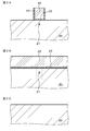
- FIGS. 1A, 1B, and 1C are schematic partial cross-sectional views of the semiconductor device of Example 1 along arrows AA, BB, and CC in FIG.
- FIG. 2 is a schematic perspective view illustrating a part of the semiconductor device according to the first embodiment.
- FIGS. 3A, 3B, and 3C are diagrams for explaining a method of manufacturing the semiconductor device according to the first embodiment, such as a substrate similar to that taken along arrows AA, BB, and CC in FIG.
- FIG. 3 is a schematic partial end view.
- FIGS. 4A, 4B, and 4C show, following FIGS. 3A, 3B, and 3C, arrows AA, arrows BB, and arrows in FIG.
- FIG. 3 is a schematic partial end view of a base and the like similar to CC.
- FIGS. 5A, 5B, and 5C show, following FIGS. 4A, 4B, and 4C, arrows AA, arrows BB, and arrows in FIG. 2 for describing the method of manufacturing the semiconductor device of the first embodiment.
- FIG. 2 is a schematic partial cross-sectional view, a partial end view, and a partial end view of a base and the like similar to the line CC.
- FIGS. 6A, 6B, and 6C show, following FIGS. 5A, 5B, and 5C, arrows AA, arrows BB, and arrows in FIG.
- FIG. 3 is a schematic partial end view of a base and the like similar to CC.
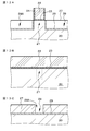
- 7A, 7B, and 7C are schematic partial cross-sectional views of the semiconductor device according to the second embodiment, which are similar to those taken along arrows AA, BB, and CC in FIG.
- FIGS. 8A, 8B, and 8C are diagrams for explaining a method of manufacturing a semiconductor device according to the second embodiment, such as a base similar to the arrows AA, BB, and CC in FIG.
- FIG. 3 is a schematic partial end view.
- FIGS. 9A, 9B, and 9C show, following FIGS.
- FIG. 2 is a schematic partial cross-sectional view, a partial end view, and a partial end view of a base and the like similar to the line CC.
- FIGS. 10A, 10B, and 10C show, following FIGS. 9A, 9B, and 9C, arrows AA, BB, and arrows in FIG. 2 for describing the method of manufacturing the semiconductor device of the second embodiment.
- FIG. 2 is a schematic partial cross-sectional view, a partial end view, and a partial end view of a base and the like similar to the line CC.
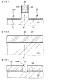
- FIGS. 11A, 11B, and 11C are schematic partial cross-sectional views of the semiconductor device according to the third embodiment, which are similar to the arrows AA, BB, and CC in FIG.
- FIGS. 12A, 12B, and 12C are diagrams for explaining a method of manufacturing the semiconductor device according to the third embodiment, such as a substrate similar to that taken along arrows AA, BB, and CC in FIG.
- FIG. 3 is a schematic partial end view.
- FIGS. 13A, 13B, and 13C show, following FIGS. 12A, 12B, and 12C, arrows AA, BB, and arrows in FIG. 2 for describing the method of manufacturing the semiconductor device of the third embodiment.
- FIG. 12A, 12B, and 12C show, following FIGS. 12A, 12B, and 12C, arrows AA, BB, and arrows in FIG. 2 for describing the method of manufacturing the semiconductor device of the third embodiment.
- FIG. 2 is a schematic partial cross-sectional view, a partial end view, and a partial end view of a base and the like similar to the line CC.
- FIGS. 14A, 14B, and 14C show, following FIGS. 13A, 13B, and 13C, arrows AA, BB, and arrows in FIG. 2 for describing the method of manufacturing the semiconductor device of the third embodiment.
- FIG. 3 is a schematic partial end view of a base and the like similar to CC.
- FIGS. 15A, 15B, and 15C show, following FIGS. 14A, 14B, and 14C, arrows AA, arrows BB, and arrows in FIG. 2 for describing the method of manufacturing the semiconductor device of the third embodiment.
- FIG. 14A, 14B, and 14C show, following FIGS. 14A, 14B, and 14C, arrows AA, arrows BB, and arrows in FIG. 2 for describing the method of manufacturing the semiconductor device of the third embodiment
- FIG. 3 is a schematic partial end view of a base and the like similar to CC.
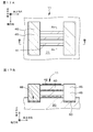
- FIG. 16 is a schematic partial end view of the semiconductor device of Example 4 along the arrow AA in FIG. 17A.
- 17A and 17B are a schematic layout view of the channel portion and the source / drain region of the semiconductor device of the fourth embodiment, respectively, and one example of the semiconductor device of the fourth embodiment along arrow BB in FIG. 17A. It is a typical partial end view of the component of a part.
- FIGS. 18A, 18B, and 18C are schematic partial end views of the base and the like similar to the arrows AA in FIG. 17 for explaining the method of manufacturing the semiconductor device of the fourth embodiment.
- FIG. 19A and 19B are schematic partial end views of a base and the like similar to those taken along arrow AA in FIG. 17 for illustrating the method of manufacturing the semiconductor device according to the fourth embodiment, following FIG. 18C. is there.
- 20A and FIG. 20B are schematic partial end views of the base and the like similar to those taken along arrow AA in FIG. 17 for illustrating the method of manufacturing the semiconductor device of Example 4 following FIG. 19B.
- FIG. 20C is a schematic partial end view of the base and the like when cut in the same manner as along the arrow BB in FIG. 21A and 21B are schematic partial end views of the base and the like similar to those taken along arrow BB in FIG. 17 for explaining the method for manufacturing the semiconductor device of Example 4 following FIG. 20C. is there.
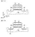
- FIG. 22A and FIG. 22B are schematic partial cross-sectional views of another example of the semiconductor device of Example 1 and Example 2 similar to the direction of arrow AA of FIG.
- FIG. 23 is a schematic partial sectional view of a conventional planar semiconductor device.
- FIGS. 24A and 24B are schematic partial end faces of a substrate and the like similar to those taken along arrows AA and BB in FIG. 2 for explaining problems in a conventional semiconductor device having a Fin structure.
- FIG. 24C and FIG. 24D are schematic partial end views of a base and the like similar to those taken along arrow CC in FIG. 2 for explaining problems in a conventional semiconductor device having a Fin structure. It is.
- Example 1 semiconductor device of the present disclosure, method of manufacturing the same, and overall Example 1 (Semiconductor device of the present disclosure and manufacturing method thereof, semiconductor device having Fin structure) 3.
- Example 2 Modification of Example 1 4.
- Example 3 another modification of Example 1 5.
- Example 4 still another modification of Example 1, a semiconductor device having a nanowire structure 6.
- the channel part is composed of a part of the base, A gate electrode is formed above the channel portion via a gate insulating film, The region of the base on which the source / drain region is to be formed is partially removed in the thickness direction such that the cross-sectional shape of the side surface of the channel portion facing the region where the source / drain region is to be formed has a drum shape.
- a drum-shaped cross-sectional shape of the side surface of the channel portion can be obtained by partially removing the substrate in the thickness direction based on a dry etching method such as an RIE method and then performing a wet etching method. Can be.
- the channel part is composed of a part of the base, A gate electrode is formed above the channel portion via a gate insulating film, After partially removing the region of the base on which the source / drain region is to be formed in the thickness direction, an offset spacer (protective layer) is formed on the obtained region where the source / drain region is to be formed and the side surface of the channel portion.
- the impurity layer may be formed via the offset spacer, and then the offset spacer may be removed.
- Examples of a material constituting the offset spacer (protective layer) include SiN, SiON, and SiOCN.
- ALD method an atomic layer deposition method
- the formation of the semiconductor layer on the impurity layer may be based on an epitaxial growth method. That is, an epitaxial CVD method can be used, but the present invention is not limited to such a method. In addition, a plasma CVD method and an atomic layer deposition method (ALD method) can also be used.
- an epitaxial CVD method can be used, but the present invention is not limited to such a method.
- a plasma CVD method and an atomic layer deposition method (ALD method) can also be used.
- an embodiment in the method of manufacturing a semiconductor device according to the present disclosure including the various preferable embodiments described above, an embodiment may be employed in which an impurity layer is formed in a region where a source / drain region is to be formed based on an ion implantation method.
- the semiconductor device of the present disclosure or a semiconductor device obtained based on the method for manufacturing a semiconductor device of the present disclosure including the various preferable embodiments described above (hereinafter, these semiconductor devices are collectively referred to as “the present disclosure” Semiconductor device etc. ").
- the channel part is composed of a part of the base,
- a gate electrode is formed above the channel portion via a gate insulating film,
- the cross-sectional shape of the side surface of the channel portion facing the side surface of the semiconductor layer may have a drum shape.
- the channel part is composed of a part of the base, A gate electrode is formed above the channel portion via a gate insulating film, An impurity layer may not be formed between the semiconductor layer and the region of the base which forms the channel portion.
- the drum shape means that the width of the upper portion located on the gate electrode side in the side surface cross section of the channel portion facing the side surface of the semiconductor layer is W TP , the lower width located on the substrate side in the side surface cross section is W BT , when the width of the cross-sectional thickness direction central portion was W CT, W CT ⁇ W TP W CT ⁇ W BT Refers to a shape that satisfies
- the channel part is composed of a part of the base, A gate electrode is formed above the channel portion via a gate insulating film, A second impurity layer is formed between the semiconductor layer and the region of the base constituting the channel portion, Assuming that the average thickness of the impurity layer is T 1 and the average thickness of the second impurity layer is T 2 , 0 ⁇ T 2 / T 1 ⁇ 0.5 Is satisfied.
- the impurity concentration C 1 of the impurity layer may be a higher form than the impurity concentration C 2 of the semiconductor layer, or alternatively, 0.1 ⁇ C 2 / C 1 ⁇ 10 Is preferably satisfied.
- the semiconductor device or the like of the present disclosure including the various preferable embodiments and configurations described above can be an embodiment having a Fin structure.
- the semiconductor device or the like of the present disclosure including the various preferable embodiments described above can be in a form having a nanowire structure or a nanosheet structure.
- the gate electrode is formed from the top surface to the side surface of the channel portion. Further, it may be formed over the bottom surface.
- a semiconductor device having such a configuration that is, a semiconductor device in which the entire outer periphery of a channel portion is surrounded by a gate electrode, is also referred to as a semiconductor device having a GAA (Gate- All-Around) structure.
- a planar semiconductor device specifically, a MOSFET
- the presence of the impurity layer is determined by secondary ion mass spectrometry (SIMS), energy dispersive X-ray analysis (EDS), scanning spreading resistance microscopy (Scanning Spreading Resistance Microscopy, SSRM), Detection can be performed by using scanning capacitance microscopy (Scanning Capacitance Microscopy, SCM) or by appropriately combining these analytical methods.
- SIMS secondary ion mass spectrometry
- EDS energy dispersive X-ray analysis
- SSRM scanning spreading resistance microscopy
- Detection can be performed by using scanning capacitance microscopy (Scanning Capacitance Microscopy, SCM) or by appropriately combining these analytical methods.
- the voltage applied to the gate electrode of the semiconductor device or the like according to the present disclosure is in a form of 1.2 volts to 3.3 volts, which is higher than 1.0 volt or less, which is a normal drive voltage of a logic circuit device.
- the present invention is not limited to such a voltage.
- a silicon semiconductor substrate In the semiconductor device and the like of the present disclosure including the various preferable embodiments and configurations described above, a silicon semiconductor substrate, a SOI (Si On Insulator) substrate, a GOI (Ge On On Insulator) substrate, a SGOI (SiGe On Insulator) substrate.
- the semiconductor layer preferably has crystallinity, but may be composed of polycrystal, or may be composed of amorphous in some cases.
- the second conductivity type when the first conductivity type is n-type, the second conductivity type is p-type, and when the first conductivity type is p-type, the second conductivity type is n. Type.
- channel portion the gate insulating film, and the gate electrode may be collectively referred to as a “channel structure portion”.
- the outer periphery of a channel portion is at least partially covered with a gate insulating film along a circumferential direction, and a gate electrode is formed over the gate insulating film. ing. It is sufficient that at least one channel structure is provided. In the case where a plurality of channel structures are provided, the channel structures may be arranged apart from each other in the thickness direction and / or the width direction (a direction orthogonal to the thickness direction) of the semiconductor device. That is, the gate insulating film and the gate electrode are formed between the channel portions, and the space between the channel portions is filled with the gate insulating film and the gate electrode.
- both ends of a wire-shaped channel portion having a diameter of, for example, 5 nm to 10 nm and made of, for example, Si or SiGe are supported by, for example, source / drain regions.
- both ends of a channel portion having a width ⁇ thickness of, for example, (10 nm to 50 nm) ⁇ (5 nm to 10 nm) and having a substantially rectangular cross section made of, for example, Si or SiGe are formed, for example. , Source / drain regions. Whether the structure is a nanowire structure or a nanosheet structure depends on the thickness and width of the material forming the channel portion.
- examples of a material forming a channel portion in the nanowire structure or the nanosheet structure include Si, SiGe, Ge, and InGaAs.
- the channel portion in the n-channel type semiconductor device can be made of Si, and the channel portion in the p-channel type semiconductor device can be made of SiGe, Ge, or InGaAs. However, it is not limited to this.
- the channel portion of the n-channel type semiconductor device is made of silicon-germanium (SiGe), The channel portion of the p-channel semiconductor device can be made of silicon (Si), germanium (Ge), or InGaAs;
- the channel portion of the n-channel semiconductor device is made of germanium (Ge), The channel portion of the p-channel semiconductor device can be made of silicon (Si), silicon-germanium (SiGe), or InGaAs;
- the channel portion of the n-channel semiconductor device is made of InGaAs,
- the channel portion of the p-channel semiconductor device can be made of silicon (Si), silicon-germanium (SiGe), or germanium (Ge).
- the semiconductor device or the like of the present disclosure has a nanowire structure or a nanosheet structure
- whether the semiconductor device is an n-channel type or a p-channel type depends solely on the value of the work function of the material forming the gate electrode. It is determined.
- the channel portion is made of Si
- TiN, TaN, Al, TiAl, and W can be used as a material forming the gate electrode.
- TiN and W can be used as a material forming the gate electrode.
- SiON and SiO 2 can be used, and a high dielectric constant material (a so-called High-k material) such as HfO 2 , HfAlON, and Y 2 O 3 can be used. .
- a semiconductor device or the like of the present disclosure having a Fin structure has a rectangular channel section formed on a base, source / drain regions formed at both ends of the channel area, and at least a top surface of the channel section. And a gate electrode formed on the gate insulating film.
- the gate insulating film only needs to be formed on at least the top surface of the channel portion, and examples include a form formed on the top surface of the channel portion and a form formed on the top surface and side surfaces of the channel portion.
- the width of the channel portion may be the same as the width of the source / drain region, or the width of the source / drain region may be wider than the width of the channel portion.
- the semiconductor device or the like of the present disclosure depends on the required specification of the semiconductor device, and thus cannot be specified unconditionally.
- a transistor that transmits and receives signals to and from the outside is configured by the semiconductor device or the like of the present disclosure, and control of an imaging element (light receiving element) in an imaging device such as a transistor that configures an analog-to-digital converter is described in the semiconductor of the present disclosure.
- a mode in which the control is performed by a device or the like and a mode in which the control of the light receiving element in the imaging device is performed by the semiconductor device or the like of the present disclosure can be exemplified. However, it is not limited to these.
- Example 1 relates to a semiconductor device of the present disclosure and a method of manufacturing the same.
- FIG. 1A, FIG. 1B and FIG. 1C show schematic partial cross-sectional views of the semiconductor device of Example 1 along arrows AA, BB and CC of FIG.
- FIG. 2 is a schematic perspective view showing a part of the semiconductor device.
- the semiconductor device 10 of the first embodiment or the second to third embodiments described below Channel unit 21, A gate electrode 22 provided to face the channel portion 21 via the gate insulating film 23, and Source / drain regions 25 provided at both ends of the channel portion 21;
- the source / drain region 25 has a first conductivity type (specifically, for example, n + ), and includes a semiconductor layer 26 formed in a concave portion 28 provided in the base 20.
- An impurity layer (high-concentration impurity layer) 30 having a second conductivity type (specifically, for example, p ++ ) different from the first conductivity type is provided between the bottom of the semiconductor layer 26 and the base 20. Are formed.
- the channel portion 21 is constituted by a part of the base 20, A gate electrode 22 is formed above the channel portion 21 with a gate insulating film 23 interposed therebetween.
- the impurity concentration C 1 of the impurity layer 30 is higher than the impurity concentration C 2 of the semiconductor layer 26.
- C 2 / C 1 0.2 It is.
- the semiconductor device 10 of the first embodiment or the second to third embodiments has a Fin structure.
- the semiconductor device 10 according to the first embodiment or the second to third embodiments having the Fin structure has a rectangular channel section 21 formed on the base 20, and formed at both ends of the channel section 21. And a gate insulating film 23 formed on at least the top surface of the channel portion 21, and a gate electrode 22 formed on the gate insulating film 23.
- the base 20 is made of a silicon semiconductor substrate.
- the width of the channel portion 21 and the width of the source / drain region 25 may be the same, and the width of the source / drain region 25 may be wider than the width of the channel portion 21.
- FIGS. 3A, 3B, 3C, and 3C are schematic partial end views or partial cross-sectional views of a substrate and the like similar to those taken along arrows AA, BB, and CC in FIG. 4A, FIG. 4B, FIG. 4C, FIG. 5A, FIG. 5B, FIG. 5C, FIG. 6A, FIG. 6B, and FIG.
- Step-100 First, after the channel portion 21 is formed, the gate electrode 22 facing the channel portion 21 via the gate insulating film 23 is formed. Specifically, after a not-shown element isolation region is formed by a well-known method, ion implantation is performed on a portion of the base 20 where the channel portion 21 is to be formed, if necessary, to form the channel portion 21. Next, a gate insulating film 23 is formed on the surface of the base 20 by thermally oxidizing the surface of the base 20, and the gate electrode 22 is formed on the gate insulating film 23 by a known method. Further, a gate sidewall 24 is formed on the side wall of the gate electrode 22 by a known method. Thus, the structure shown in FIGS. 3A, 3B and 3C can be obtained.
- Step-110 the region of the base 20 where the source / drain region 25 is to be formed is partially removed in the thickness direction to obtain a source / drain region formation expected region 28A. More specifically, an etching mask (not shown) is formed in a desired region, and a region of the base 20 where the source / drain region 25 is to be formed is partially removed in a thickness direction by a known method. After forming the concave portion 28, the etching mask is removed. In this way, as shown in FIGS. 4A, 4B and 4C, a source / drain region formation expected region 28A can be obtained.
- an impurity layer 30 having the second conductivity type is formed in the source / drain region formation region 28A (the bottom of the concave portion 28).
- the insulating layer 27 is formed on the region of the base 20 except for the region 28A where the source / drain region is to be formed by a known method.
- a concave portion 28 is provided in the insulating layer 27, and a source / drain region formation region 28 ⁇ / b> A is exposed at the bottom of the concave portion 28.
- FIGS. 5A, 5B and 5C can be obtained.
- an impurity having the second conductivity type (for example, p ++ ) is formed at the bottom of the concave portion 28 corresponding to the source / drain region formation planned region 28A based on the ion implantation method.
- an activation annealing process is performed, and then the ion implantation mask is removed.
- a source / drain region 25 including a semiconductor layer 26 having a first conductivity type (for example, n + ) different from the second conductivity type is formed on the impurity layer 30.
- the formation of the semiconductor layer 26 on the impurity layer 30 is based on an epitaxial growth method. Specifically, a semiconductor layer 26 made of silicon containing an impurity having the first conductivity type is grown from the impurity layer 30 made of silicon by an epitaxial growth method. Thus, the structure shown in FIGS. 1A, 1B, and 1C can be obtained.
- an opening is formed in the interlayer insulating layer located above the gate electrode 22 and the source / drain region 25, and a connection is made from inside the opening to over the interlayer insulating layer.
- a hole and a wiring may be formed.
- a predetermined region of the base 20 is partially removed in the thickness direction to form a source / drain region formed of the base 20.
- the scheduled area 28A ' is obtained.
- the structure shown in FIGS. 24A, 24B, and 24C can be obtained.
- ion implantation is performed on the source / drain region formation region 28A 'formed of the base 20 to form the source / drain region 25' (see FIG. 24D). In this ion implantation, a crystal defect occurs in a portion of the base 20 constituting the source / drain region 25 '.
- the crystal defect is repaired by recrystallization in the bottom 25 ′′ of the source / drain region 25 ′. It is difficult for the portion of the source / drain region 25 ′ located above “” to recrystallize, and it is difficult to recrystallize the entire source / drain region 25 ′.
- the source / drain region has a first conductivity type and includes a semiconductor layer formed in a concave portion provided in the base, and a gap between the bottom of the semiconductor layer and the base is provided. Is formed with an impurity layer having a second conductivity type different from the first conductivity type, that is, an impurity layer is formed between the bottom of the semiconductor layer forming the source / drain region and the base. Therefore, in the method of manufacturing a semiconductor device according to the first embodiment, an impurity layer having the second conductivity type is formed in a region where a source / drain region is to be formed, and then a second conductive layer is formed on the impurity layer.
- the source / drain region including the semiconductor layer having the first conductivity type different from the mold is formed, generation of a leak current can be suppressed.
- the impurity layer having the second conductivity type is formed in the region where the source / drain region is to be formed by ion implantation, the channel portion and the source / drain region are not formed. It is difficult to form a high-concentration impurity layer in a boundary region therebetween, and it is possible to suppress the occurrence of a problem that the resistance of the channel region is increased.
- the second embodiment is a modification of the first embodiment.
- it is difficult to form a high-concentration impurity layer in the boundary region 21 ′ between the channel portion 21 and the source / drain region 25.
- the boundary region 21 ′ between the channel portion 21 and the source / drain region 25 is slightly, but slightly, highly doped with an impurity layer (the second impurity layer 31). ) May be formed (see FIG. 22A, which is a schematic partial cross-sectional view of another example of the semiconductor device of Example 1 similar to the direction of arrow AA in FIG. 2).
- the cross-sectional shape of the side surface 21A of the channel portion 21 facing the side surface of the semiconductor layer 26 into a drum shape, in the boundary region 21 ′ between the channel portion 21 and the source / drain region 25, The formation of a high-concentration impurity layer is more reliably suppressed.
- This drum-shaped cross section is a shape that may be adopted to increase the volume of the source / drain region.
- FIGS. 7A, 7B, and 7C are schematic partial cross-sectional views of the semiconductor device of Example 2, which are similar to those taken along arrows AA, BB, and CC in FIG.
- the cross-sectional shape of the side surface 21A of the channel portion 21 facing the side surface of the semiconductor layer 26 has a drum shape.
- the channel portion 21 is formed of a part of the base 20, and is provided above the channel portion 21 via the gate insulating film 23.
- a gate electrode 22 is formed.
- no impurity layer (second impurity layer 31) is further formed between the semiconductor layer 26 and the region of the base 20 forming the channel portion 21.
- W CT ⁇ W TP W CT ⁇ W BT To be satisfied.
- the cross-sectional shape (hourglass shape) of the side surface of the channel portion 21 facing the side surface of the semiconductor layer 26 is the same as that of [Step-100] of the first embodiment, and then the [Step-] of the first embodiment is performed. 110], the region of the base 20 on which the source / drain region 25 is to be formed is formed such that the cross-sectional shape of the side surface 21A of the channel portion 21 facing the source / drain region formation region 28A has a drum shape. It may be partially removed in the thickness direction. More specifically, partial removal of the substrate 20 in the thickness direction may be performed based on a dry etching method such as an RIE method and then a wet etching method. Thus, as shown in FIGS.
- a source / drain region formation expected region 28A can be obtained.
- the cross-sectional shape of the side surface 21A of the channel portion 21 can be made drum-shaped by etching.
- the cross-sectional shape of the channel portion 21 obtained by etching changes depending on the plane orientation of the substrate 20 and the direction in which the channel portion 21 extends.
- FIGS. 9A, 9B and 9C After that, by performing the same steps as [Step-120] of Example 1, the structure shown in FIGS. 9A, 9B and 9C can be obtained. 10A, 10B, and 10C can be obtained by performing the same steps. Further, by performing the same steps as [Step-130] of the first embodiment, FIGS. The structure shown in FIGS. 7B and 7C can be obtained.
- the third embodiment is also a modification of the first embodiment.
- the cross-sectional shape of the side surface 21A of the channel portion 21 facing the side surface of the semiconductor layer 26 has a drum shape, the boundary region between the channel portion 21 and the source / drain region 25 is formed. It is difficult to form a high-concentration impurity layer further in 21 ′.
- a small amount of a high-concentration impurity layer may be formed below the boundary region 21 ′ between the channel portion 21 and the source / drain region 25.
- an impurity layer 31 is formed (see FIG.
- an offset spacer (protective layer) 29 is formed on the side surface of the channel portion 21 during the manufacturing process of the semiconductor device, so that the boundary region 21 between the channel portion 21 and the source / drain region 25 is formed.
- the formation of a high-concentration impurity layer is more reliably suppressed.
- the [Step- 120] to obtain the structure shown in FIG. 5A, FIG. 5B and FIG. 5C. Then, the obtained source / drain region formation region 28A and the side surface of the channel portion 21 are offset by ion implantation. A spacer (protective layer) 29 is formed.
- the offset spacer 29 is made of SiO 2 , SiN or the like, and has a thickness of about 1 to 5 nm. Thus, the structure shown in FIGS. 12A, 12B and 12C can be obtained.
- the same step as [Step-120] in Example 1 see FIGS.
- Embodiment 4 is also a modification of Embodiment 1, but the semiconductor device has a nanowire structure or nanosheet structure. In Embodiment 4, specifically, it has a nanowire structure.
- the gate electrode 22 is formed from the top surface to the side surface of the channel portion 21 and further from the bottom surface, and has a GAA structure.
- FIG. 16 is a schematic partial end view of the semiconductor device of Example 4 along arrow AA in FIG. 17A, and is a schematic view of the semiconductor device of Example 4 along arrow BB in FIG. 17A.
- FIG. 17B is a partial end view
- FIG. 17A is a schematic layout view of the channel portion and the source / drain regions of the semiconductor device of the fourth embodiment. 17A and 17B, illustration of the gate electrode and the gate insulating film is omitted.
- the semiconductor device 11 of the fourth embodiment also Channel section 41, A gate electrode 42 provided to face the channel portion 41 via the gate insulating film 43; Source / drain regions 45 provided at both ends of the channel portion 41, With The source / drain region 45 has a first conductivity type (specifically, for example, n + ), and includes a semiconductor layer 46 formed in a concave portion 48 provided in the base 20 made of a silicon semiconductor substrate. And An impurity layer (high-concentration impurity layer) 50 having a second conductivity type (specifically, for example, p ++ ) different from the first conductivity type is provided between the bottom of the semiconductor layer 46 and the base 20. Are formed.
- the semiconductor device 11 of the fourth embodiment has at least two channel structures 40 having the nanowire structure 40A (in the illustrated example, two in the thickness direction).
- the semiconductor devices 11 are arranged apart from each other in the thickness direction.
- three nanowire structures 40A are provided in the width direction.
- the channel structure section 40 includes a channel section 41 made of silicon, a gate insulating film 43, and a gate electrode 42. Further, a gate insulating film 43 and a gate electrode 42 are formed between the channel portions 41 and the channel portion 41, and the gate insulating film 43 and the gate electrode 42 are provided between the channel portions 41 and 41. Embedded.
- the semiconductor device is, for example, an n-channel type.
- Examples of the material forming the gate electrode 42 include TiN, TaN, Al, TiAl, and W.
- the gate insulating film 43A constituting a part of the gate insulating film 43 is made of SiON, and the gate insulating film 43B constituting the rest of the gate insulating film 43 is made of a high dielectric constant material, specifically, HfO 2. .
- FIGS. 18A, 18B, 18C, 19, 19B, 20A, 20B, 20C, 21A, and 21B are schematic partial end views similar to those taken along arrow AA in FIG. 17A.
- 21A and 21B are schematic partial end views similar to those taken along arrow BB in FIG. 17A.
- Step-400 First, a first sacrificial layer 61 made of SiGe is formed on a desired region of the base 20, and then a first semiconductor layer 62 made of Si is formed on the first sacrificial layer 61.
- Step-400A Specifically, first, a first sacrificial layer 61 made of SiGe is formed on the entire surface of the base 20 by epitaxial CVD, and then an etching resist having a desired resist pattern is formed on the first sacrificial layer 61. Then, after patterning the first sacrificial layer 61, the first sacrificial layer 61 can be formed on a desired region by removing the etching resist.
- Step-400B Next, after forming a first semiconductor layer 62 made of Si on the entire surface based on the epitaxial CVD method, an etching resist having a desired resist pattern is formed on the first semiconductor layer 62. Then, after patterning the first semiconductor layer 62, the first semiconductor layer 62 can be formed on the first sacrificial layer 61 by removing the etching resist.
- Step-410 a second sacrificial layer 63 made of SiGe is formed on the first semiconductor layer 62, and then a second semiconductor layer 64 made of Si is formed on the second sacrificial layer 63.
- Step-410A Specifically, after forming a second sacrificial layer 63 made of SiGe over the entire surface based on the epitaxial CVD method, an etching resist having a desired resist pattern is formed on the second sacrificial layer 63. Then, after patterning the second sacrifice layer 63, the second sacrifice layer 63 can be formed on the first semiconductor layer 62 by removing the etching resist.
- Step-410B Next, after forming a second semiconductor layer 64 made of Si on the entire surface based on the epitaxial CVD method, an etching resist having a desired resist pattern is formed on the second semiconductor layer 64. Then, after patterning the second semiconductor layer 64, the resist for etching is removed, whereby the second semiconductor layer 64 can be formed on the second sacrificial layer 63. Thus, the structure shown in FIG. 18A can be obtained.
- Step-420 Thereafter, a laminated structure 40 ′′ including the first sacrifice layer 61, the first semiconductor layer 62, the second sacrifice layer 63, and the second semiconductor layer 64 is formed, and then the second sacrifice layer 63 in the laminated structure 40 ′′ is formed. A part of the first sacrificial layer 61 is removed.
- Step-420A Specifically, an etching resist 81 having a desired resist pattern is formed on the entire surface (see FIG. 18B). Then, the second semiconductor layer 64, the second sacrifice layer 63, the first semiconductor layer 62, and the first sacrifice layer 61 are patterned, and a part of the base 20 is further etched. Depending on the width of the etching resist 81, a nanowire structure 40A is obtained, or alternatively, a nanosheet structure is obtained. Thus, the structure shown in FIG. 18C can be obtained.
- Step-420B Next, after an insulating material layer made of SiO 2 is formed on the entire surface based on the CVD method, a planarization process is performed, whereby the element isolation region 71 can be obtained (see FIG. 19A).
- Step-420C Then, the first sacrifice layer 61 and the second sacrifice layer 63 made of SiGe are removed using an etchant having an etching selectivity with respect to the material (Si) forming the first semiconductor layer 62 and the second semiconductor layer 64. . Both ends of the channel portion 41 made of the nanowire structure 40A are supported by the support made of the laminated structure 40 ′′. Thereafter, the etching resist 81 is removed. Thus, the structure shown in FIG. 19B can be obtained. .
- Step-430 After that, the gate insulating films 43A and 43B and the gate electrode 42 are formed in the channel portion 41.
- Step-430A Specifically, first, a resist layer (not shown) having a desired resist pattern is formed, and a thermal oxidation process is performed on the channel portion 41, thereby forming a portion 43A of the gate insulating film made of SiON ( See FIG. 20A). By performing the thermal oxidation treatment, the cross-sectional shape of the channel portion 41 having the nanowire structure becomes circular.
- Step-430B Next, the remaining portion 43B of the gate insulating film made of HfO 2 is formed on the gate insulating film 43A based on the ALD method (see FIG. 20B).
- Step-430C Thereafter, a material layer forming the gate electrode is formed on the entire surface based on the CVD method, and the material layer is patterned to form the gate electrode 42 on the gate insulating film 43 (see FIG. 20C).
- the gate electrode 42 facing the channel portion 41 via the gate insulating film can be formed.
- Step-440 the region of the base 20 where the source / drain region 45 is to be formed is partially removed in the thickness direction to obtain a source / drain region formation scheduled region 48A (see FIG. 21A).
- the support portion composed of the laminated structure 40 ′′ supporting both ends of the channel portion 41 is removed, the base 20 is exposed, and the region of the base 20 is partially removed in the thickness direction.
- the concave portion 48 can be obtained, and the concave portion 48 corresponds to the source / drain region formation scheduled region 48A.
- an impurity layer 50 having the second conductivity type (specifically, for example, p ++ ) is formed in the source / drain region formation planned region 48A (the bottom of the concave portion 48) (see FIG. 21B).
- a desired region is covered with an ion implantation mask, and an impurity layer 50 having the second conductivity type is formed at the bottom of the concave portion 48 corresponding to the source / drain region formation planned region 48A based on the ion implantation method.
- activation annealing is performed, and then the ion implantation mask is removed.
- a source / drain region 45 including a semiconductor layer 46 having a first conductivity type (specifically, for example, n + ) different from the second conductivity type is formed on the impurity layer 50.
- the formation of the semiconductor layer 46 on the impurity layer 50 is based on an epitaxial growth method. Specifically, a semiconductor layer 46 made of silicon containing an impurity having the first conductivity type is grown from the impurity layer 50 made of silicon based on an epitaxial growth method.
- the semiconductor device having the nanowire structure shown in FIGS. 16, 17A and 17B can be obtained.
- an interlayer insulating layer is formed on the entire surface, an opening is formed in the interlayer insulating layer located above the gate electrode 42 and the source / drain region 45, and a connection hole extends from inside the opening to over the interlayer insulating layer. And wiring may be formed.
- the present disclosure has been described based on the preferred embodiments.
- the configuration, the structure, the material forming the semiconductor device, and the method of manufacturing the semiconductor device of the semiconductor device described in the embodiments are merely examples, and can be appropriately changed.
- the order of the steps in the method of manufacturing a semiconductor device in each embodiment can be appropriately changed as desired.
- the channel portion is described based solely on the nanowire structure.
- the channel portion may have a nanosheet structure.
- the configuration in which the channel portion extends in parallel with the surface of the substrate has been described.
- the channel portion may be configured to extend perpendicular to the surface of the substrate.
- the structure of the semiconductor device of the present disclosure can be applied to a source / drain region (source region or drain region) located below the channel portion.
- the semiconductor device is an n-channel type, but may be a p-channel type.
- the material constituting the semiconductor device may be changed as appropriate.
- As a base, an SOI substrate, a GOI substrate, or an SGOI substrate can be used instead of the silicon semiconductor substrate.
- the present disclosure may have the following configurations.
- ⁇ Semiconductor device >> Channel section, A gate electrode provided to face the channel portion via the gate insulating film, and Source / drain regions provided at both ends of the channel portion, With The source / drain region has a first conductivity type and includes a semiconductor layer formed in a concave portion provided in the base, A semiconductor device in which an impurity layer having a second conductivity type different from the first conductivity type is formed between a bottom of a semiconductor layer and a base.
- the channel portion is composed of a part of the base,
- the semiconductor device according to [A01] wherein a cross-sectional shape of a side surface of the channel portion facing the side surface of the semiconductor layer has a drum shape.
- the channel portion is composed of a part of the base, The semiconductor device according to [A01] or [A02], wherein an impurity layer is not formed between a region of the base included in the channel portion and the semiconductor layer.
- the channel portion is composed of a part of the base, A second impurity layer is formed between the semiconductor layer and the region of the base constituting the channel portion, Assuming that the average thickness of the impurity layer is T 1 and the average thickness of the second impurity layer is T 2 , 0 ⁇ T 2 / T 1 ⁇ 0.5 [A01]
- [A05] The semiconductor device according to any one of [A01] to [A04], wherein the impurity concentration C 1 of the impurity layer is higher than the impurity concentration C 2 of the semiconductor layer.
- [A06] When the impurity concentration of the impurity layer is C 1 and the impurity concentration of the semiconductor layer is C 2 , 0.1 ⁇ C 2 / C 1 ⁇ 10
- the semiconductor device according to any one of [A01] to [A04] which satisfies the following.
- [A07] The semiconductor device according to any one of [A01] to [A06] having a Fin structure.
- [A08] The semiconductor device according to any one of [A01] to [A06], having a nanowire structure or a nanosheet structure.
- the channel portion is composed of a part of the base, The region of the base on which the source / drain region is to be formed is partially removed in the thickness direction so that the cross-sectional shape of the side surface of the channel portion facing the region where the source / drain region is to be formed has a drum shape [B01].
- the channel portion is composed of a part of the base, After partially removing the region of the base on which the source / drain region is to be formed in the thickness direction, an offset spacer is formed on the obtained region where the source / drain region is to be formed and the side surface of the channel portion.
- Reference numerals 10, 11 semiconductor device, 20: base (silicon semiconductor substrate), 21: channel portion, 21 ': boundary region, 21A: side surface of channel portion, 22: gate electrode 23 gate insulating film 24 gate side wall 25 source / drain region 26 semiconductor layer 27 insulating layer 28 recess 28A Source / drain region formation region, 29: offset spacer (protective layer), 30: impurity layer, 31: second impurity layer, 40: channel structure, 40A: nanowire Structure, 40 "... laminated structure, 41 ... channel portion, 42 ... gate electrode, 43, 43A, 43B ... gate insulating film, 45 ... source / drain region, 46 ... Semiconductor layer, 48 ... concave , 48A ... source / drain region formation planned region, 50 ... impurity layer, 61, 63 ... sacrifice layer, 62, 64 ... semiconductor layer, 71 ... element isolation region, 81 ... Etching resist
Landscapes
- Engineering & Computer Science (AREA)
- Chemical & Material Sciences (AREA)
- Nanotechnology (AREA)
- Physics & Mathematics (AREA)
- Mathematical Physics (AREA)
- Theoretical Computer Science (AREA)
- Crystallography & Structural Chemistry (AREA)
- Insulated Gate Type Field-Effect Transistor (AREA)
- Thin Film Transistor (AREA)
Abstract
本開示の半導体装置は、チャネル部21、ゲート絶縁膜23を介してチャネル部21と対向して設けられたゲート電極22、並びに、チャネル部22の両端に設けられたソース/ドレイン領域25を備えており、ソース/ドレイン領域25は、第1の導電型を有し、基体20に設けられた凹部28内に形成された半導体層26を備えており、半導体層26の底部と基体20との間には、第1の導電型とは異なる第2の導電型を有する不純物層30が形成されている。
Description
本開示は、半導体装置及びその製造方法に関する。
図23に模式的な一部断面図を示すような従来のプレーナ型半導体装置(具体的には、MOSFET)においては、逆バイアスp-n接合リーク電流(以下、単に、『リーク電流』と呼ぶ)の発生が大きな問題である。尚、図23において、このリーク電流を、白抜きの矢印で示す。そして、このようなリーク電流の発生の抑制には、イオン注入に基づく不純物プロファイル制御が有効である(例えば、特開2009-026940号公報参照)。ところで、イオン注入に基づく不純物プロファイル制御を行うと、ソース/ドレイン領域等に結晶欠陥が生じる。然るに、例えば、Fin構造を有する半導体装置においては、後述するように、生じた結晶欠陥の修復のために再結晶化を行うことが困難である。半導体装置の電源電圧Vddは低下する傾向にあり、低い電源電圧Vddではこのようなリーク電流の発生は大きな問題とはなり難い。しかしながら、電源電圧Vddが、例えば、1.5ボルト乃至3.3ボルトと高い場合、このようなリーク電流の発生は、依然として大きな問題である。
また、このようなリーク電流の発生を抑制する技術が、例えば、特開2010-010587号公報からも周知である。即ち、この特許公開公報に開示された半導体素子は、
半導体基板、
半導体基板に設けられた凸領域、
凸領域上に設けられたゲート絶縁膜、
ゲート絶縁膜の下の凸領域内に位置するチャネル領域、
凸領域の両側に設けられ、チャネル領域の両側にエクステンションを有するソース/ドレイン領域、及び、
凸領域とソース/ドレイン領域との間に設けられ、凸領域と接触する部分に境界を有して設けられたhalo層、
を備えている。そして、この半導体素子は、
半導体基板上にゲート絶縁膜を介してゲート電極を形成する工程と、
ゲート電極の側面にゲート側壁を形成する工程と、
ゲート側壁が形成されたゲート電極をマスクとして、半導体基板をエッチングする工程と、
半導体基板をエッチングする工程においてエッチングされた半導体基板上に、halo層をエピタキシャル成長させる工程と、
halo層上にソースドレイン領域をエピタキシャル成長させる工程、
とを備える半導体素子の製造方法によって製造される。エッチングされた半導体基板上にエピタキシャル成長法によってhalo層を形成することができるので、リーク電流の発生を抑制することができるとされている。
半導体基板、
半導体基板に設けられた凸領域、
凸領域上に設けられたゲート絶縁膜、
ゲート絶縁膜の下の凸領域内に位置するチャネル領域、
凸領域の両側に設けられ、チャネル領域の両側にエクステンションを有するソース/ドレイン領域、及び、
凸領域とソース/ドレイン領域との間に設けられ、凸領域と接触する部分に境界を有して設けられたhalo層、
を備えている。そして、この半導体素子は、
半導体基板上にゲート絶縁膜を介してゲート電極を形成する工程と、
ゲート電極の側面にゲート側壁を形成する工程と、
ゲート側壁が形成されたゲート電極をマスクとして、半導体基板をエッチングする工程と、
半導体基板をエッチングする工程においてエッチングされた半導体基板上に、halo層をエピタキシャル成長させる工程と、
halo層上にソースドレイン領域をエピタキシャル成長させる工程、
とを備える半導体素子の製造方法によって製造される。エッチングされた半導体基板上にエピタキシャル成長法によってhalo層を形成することができるので、リーク電流の発生を抑制することができるとされている。
しかしながら、特開2010-010587号公報に開示された半導体素子の製造方法に基づき得られた半導体素子にあっては、halo層は、凸領域とソース/ドレイン領域との間の境界領域にも形成されてしまう。そして、このような境界領域に高濃度の不純物層が形成されると、チャネル領域が高抵抗化してしまうといった問題が生じる。
従って、本開示の目的は、リーク電流の発生抑制、及び、チャネル部の高抵抗化の抑制を図り得る構成、構造の半導体装置、及び、係る半導体装置の製造方法を提供することにある。
上記の目的を達成するための本開示の半導体装置は、
チャネル部、
ゲート絶縁膜を介してチャネル部と対向して設けられたゲート電極、並びに、
チャネル部の両端に設けられたソース/ドレイン領域、
を備えており、
ソース/ドレイン領域は、第1の導電型を有し、基体に設けられた凹部内に形成された半導体層を備えており、
半導体層の底部と基体との間には、第1の導電型とは異なる第2の導電型を有する不純物層が形成されている。
チャネル部、
ゲート絶縁膜を介してチャネル部と対向して設けられたゲート電極、並びに、
チャネル部の両端に設けられたソース/ドレイン領域、
を備えており、
ソース/ドレイン領域は、第1の導電型を有し、基体に設けられた凹部内に形成された半導体層を備えており、
半導体層の底部と基体との間には、第1の導電型とは異なる第2の導電型を有する不純物層が形成されている。
上記の目的を達成するための本開示の半導体装置の製造方法は、
チャネル部、
ゲート絶縁膜を介してチャネル部と対向して設けられたゲート電極、並びに、
チャネル部の両端に設けられたソース/ドレイン領域、
を備えた半導体装置の製造方法であって、
チャネル部を形成した後、ゲート絶縁膜を介してチャネル部に対向したゲート電極を形成し、次いで、
ソース/ドレイン領域を形成すべき基体の領域を厚さ方向に部分的に除去し、ソース/ドレイン領域形成予定領域を得た後、
ソース/ドレイン領域形成予定領域に、第2導電型を有する不純物層を形成し、次いで、
不純物層の上に、第2導電型とは異なる第1導電型を有する半導体層を備えたソース/ドレイン領域を形成する、
各工程を有する。
チャネル部、
ゲート絶縁膜を介してチャネル部と対向して設けられたゲート電極、並びに、
チャネル部の両端に設けられたソース/ドレイン領域、
を備えた半導体装置の製造方法であって、
チャネル部を形成した後、ゲート絶縁膜を介してチャネル部に対向したゲート電極を形成し、次いで、
ソース/ドレイン領域を形成すべき基体の領域を厚さ方向に部分的に除去し、ソース/ドレイン領域形成予定領域を得た後、
ソース/ドレイン領域形成予定領域に、第2導電型を有する不純物層を形成し、次いで、
不純物層の上に、第2導電型とは異なる第1導電型を有する半導体層を備えたソース/ドレイン領域を形成する、
各工程を有する。
以下、図面を参照して、実施例に基づき本開示を説明するが、本開示は実施例に限定されるものではなく、実施例における種々の数値や材料は例示である。尚、説明は、以下の順序で行う。
1.本開示の半導体装置及びその製造方法、全般に関する説明
2.実施例1(本開示の半導体装置及びその製造方法、Fin構造を有する半導体装置)
3.実施例2(実施例1の変形)
4.実施例3(実施例1の別の変形)
5.実施例4(実施例1の更に別の変形、ナノワイヤー構造を有する半導体装置)
6.その他
1.本開示の半導体装置及びその製造方法、全般に関する説明
2.実施例1(本開示の半導体装置及びその製造方法、Fin構造を有する半導体装置)
3.実施例2(実施例1の変形)
4.実施例3(実施例1の別の変形)
5.実施例4(実施例1の更に別の変形、ナノワイヤー構造を有する半導体装置)
6.その他
〈本開示の半導体装置及びその製造方法、全般に関する説明〉
本開示の半導体装置の製造方法において、
チャネル部は基体の一部から構成されており、
チャネル部の上方に、ゲート絶縁膜を介してゲート電極が形成されており、
ソース/ドレイン領域形成予定領域と対向するチャネル部の側面の断面形状が鼓形状となるように、ソース/ドレイン領域を形成すべき基体の領域を厚さ方向に部分的に除去する形態とすることができる。このようなチャネル部の側面の鼓形状の断面形状は、基体の厚さ方向における部分的な除去を、RIE法等のドライエッチング法に基づき行った後、ウエットエッチング法を行うことで、得ることができる。
本開示の半導体装置の製造方法において、
チャネル部は基体の一部から構成されており、
チャネル部の上方に、ゲート絶縁膜を介してゲート電極が形成されており、
ソース/ドレイン領域形成予定領域と対向するチャネル部の側面の断面形状が鼓形状となるように、ソース/ドレイン領域を形成すべき基体の領域を厚さ方向に部分的に除去する形態とすることができる。このようなチャネル部の側面の鼓形状の断面形状は、基体の厚さ方向における部分的な除去を、RIE法等のドライエッチング法に基づき行った後、ウエットエッチング法を行うことで、得ることができる。
あるいは又、本開示の半導体装置の製造方法において、
チャネル部は基体の一部から構成されており、
チャネル部の上方に、ゲート絶縁膜を介してゲート電極が形成されており、
ソース/ドレイン領域を形成すべき基体の領域を厚さ方向に部分的に除去した後、得られたソース/ドレイン領域形成予定領域及びチャネル部の側面にオフセットスペーサー(保護層)を形成し、次いで、オフセットスペーサーを介して不純物層を形成し、その後、オフセットスペーサーを除去する形態とすることができる。オフセットスペーサー(保護層)を構成する材料として、例えば、SiN、SiON、SiOCNを挙げることができる。オフセットスペーサーの形成方法として、原子層堆積法(ALD法)を挙げることができる。
チャネル部は基体の一部から構成されており、
チャネル部の上方に、ゲート絶縁膜を介してゲート電極が形成されており、
ソース/ドレイン領域を形成すべき基体の領域を厚さ方向に部分的に除去した後、得られたソース/ドレイン領域形成予定領域及びチャネル部の側面にオフセットスペーサー(保護層)を形成し、次いで、オフセットスペーサーを介して不純物層を形成し、その後、オフセットスペーサーを除去する形態とすることができる。オフセットスペーサー(保護層)を構成する材料として、例えば、SiN、SiON、SiOCNを挙げることができる。オフセットスペーサーの形成方法として、原子層堆積法(ALD法)を挙げることができる。
更には、以上に説明した各種の好ましい形態を含む本開示の半導体装置の製造方法において、不純物層の上における半導体層の形成は、エピタキシャル成長法に基づく形態とすることができる。即ち、エピタキシャルCVD法を挙げることができるが、このような方法に限定するものではなく、その他、プラズマCVD法、原子層堆積法(ALD法)を挙げることもできる。
更には、以上に説明した各種の好ましい形態を含む本開示の半導体装置の製造方法において、ソース/ドレイン領域形成予定領域に、不純物層をイオン注入法に基づき形成する形態とすることができる。
本開示の半導体装置、あるいは、以上に説明した各種の好ましい形態を含む本開示の半導体装置の製造方法に基づき得られた半導体装置(以下、これらの半導体装置を総称して、便宜上、『本開示の半導体装置等』と呼ぶ場合がある)において、
チャネル部は基体の一部から構成されており、
チャネル部の上方に、ゲート絶縁膜を介してゲート電極が形成されており、
半導体層の側面と対向するチャネル部の側面の断面形状は鼓形状を有する構成とすることができる。そして、このような構成を含む本開示の半導体装置等において、
チャネル部は基体の一部から構成されており、
チャネル部の上方に、ゲート絶縁膜を介してゲート電極が形成されており、
チャネル部を構成する基体の領域と半導体層との間に不純物層は形成されていない構成とすることができる。ここで、鼓形状とは、半導体層の側面と対向するチャネル部の側面断面のゲート電極側に位置する上部の幅をWTP、側面断面の基体側に位置する下部の幅をWBT、側面断面の厚さ方向中央部の幅をWCTとしたとき、
WCT<WTP
WCT<WBT
を満足する形状を指す。
チャネル部は基体の一部から構成されており、
チャネル部の上方に、ゲート絶縁膜を介してゲート電極が形成されており、
半導体層の側面と対向するチャネル部の側面の断面形状は鼓形状を有する構成とすることができる。そして、このような構成を含む本開示の半導体装置等において、
チャネル部は基体の一部から構成されており、
チャネル部の上方に、ゲート絶縁膜を介してゲート電極が形成されており、
チャネル部を構成する基体の領域と半導体層との間に不純物層は形成されていない構成とすることができる。ここで、鼓形状とは、半導体層の側面と対向するチャネル部の側面断面のゲート電極側に位置する上部の幅をWTP、側面断面の基体側に位置する下部の幅をWBT、側面断面の厚さ方向中央部の幅をWCTとしたとき、
WCT<WTP
WCT<WBT
を満足する形状を指す。
あるいは又、本開示の半導体装置等において、
チャネル部は基体の一部から構成されており、
チャネル部の上方に、ゲート絶縁膜を介してゲート電極が形成されており、
チャネル部を構成する基体の領域と半導体層との間には第2の不純物層が形成されており、
不純物層の平均厚さをT1、第2の不純物層の平均厚さをT2としたとき、
0≦T2/T1≦0.5
を満足する構成とすることができる。
チャネル部は基体の一部から構成されており、
チャネル部の上方に、ゲート絶縁膜を介してゲート電極が形成されており、
チャネル部を構成する基体の領域と半導体層との間には第2の不純物層が形成されており、
不純物層の平均厚さをT1、第2の不純物層の平均厚さをT2としたとき、
0≦T2/T1≦0.5
を満足する構成とすることができる。
以上に説明した各種の好ましい形態、構成を含む本開示の半導体装置等において、不純物層の不純物濃度C1は、半導体層の不純物濃度C2よりも高い形態とすることができ、あるいは又、
0.1≦C2/C1≦10
を満足することが好ましい。
0.1≦C2/C1≦10
を満足することが好ましい。
以上に説明した各種の好ましい形態、構成を含む本開示の半導体装置等は、Fin構造を有する形態とすることができる。あるいは又、以上に説明した各種の好ましい形態を含む本開示の半導体装置等は、ナノワイヤー構造又はナノシート構造を有する形態とすることができ、この場合、ゲート電極は、チャネル部の頂面から側面、更には、底面に亙り形成されている形態とすることができる。尚、このような形態の半導体装置、即ち、チャネル部の全外周がゲート電極で囲まれた半導体装置は、GAA(Gate- All-Around)構造を有する半導体装置とも呼ばれる。但し、本開示の半導体装置等から、プレーナ型半導体装置(具体的には、MOSFET)を構成することもできる。
本開示の半導体装置等において、不純物層の存在は、二次イオン質量分析法(SIMS)、エネルギー分散型X線分析法(EDS)、走査型拡がり抵抗顕微鏡法(Scanning Spreading Resistance Microscopy,SSRM)、走査型キャパシタンス顕微鏡法(Scanning Capacitance Microscopy,SCM)等を用いて、あるいは、これらの分析法を適宜組み合わせて検出することができる。
本開示の半導体装置等のゲート電極に印加される電圧は、論理回路デバイスの通常の駆動電圧である1.0ボルト以下よりも高い、1.2ボルト乃至3.3ボルトである形態とすることができるが、このような電圧に限定するものではない。
以上に説明した各種の好ましい形態、構成を含む本開示の半導体装置等にあっては、基体として、シリコン半導体基板や、SOI(Si On Insulator)基板、GOI(Ge On Insulator)基板、SGOI(SiGe On Insulator)基板を挙げることができる。半導体層は、結晶性を有することが好ましいが、多結晶から構成されていてもよいし、場合によっては非晶質から構成されていてもよい。本開示の半導体装置等において、第1の導電型をn型とする場合、第2の導電型はp型であり、第1の導電型をp型とする場合、第2の導電型はn型である。
以下の説明において、チャネル部、ゲート絶縁膜及びゲート電極を総称して、『チャネル構造部』と呼ぶ場合がある。
ナノワイヤー構造又はナノシート構造を有する本開示の半導体装置等において、チャネル部の外周は、周方向に沿って少なくとも部分的にゲート絶縁膜によって覆われており、ゲート絶縁膜上にゲート電極が形成されている。チャネル構造部は、1以上、設けられていればよい。チャネル構造部が、複数、設けられている場合、チャネル構造部を、半導体装置の厚さ方向及び/又は幅方向(厚さ方向と直交する方向)において、相互に離間して配置すればよい。即ち、チャネル部とチャネル部との間には、ゲート絶縁膜及びゲート電極が形成されており、チャネル部とチャネル部との間は、ゲート絶縁膜及びゲート電極で埋め込まれている。ナノワイヤー構造にあっては、直径が、例えば、5nm乃至10nmの、例えばSiやSiGe等から成るワイヤー状のチャネル部の両端が、例えば、ソース/ドレイン領域によって支持されている。また、ナノシート構造にあっては、幅×厚さが、例えば、(10nm乃至50nm)×(5nm乃至10nm)の、例えばSiやSiGe等から成る断面形状が略矩形のチャネル部の両端が、例えば、ソース/ドレイン領域によって支持されている。ナノワイヤー構造となるか、ナノシート構造となるかは、チャネル部を構成する材料の厚さ、幅に依存する。
本開示の半導体装置等がナノワイヤー構造又はナノシート構造を有する場合、ナノワイヤー構造やナノシート構造におけるチャネル部を構成する材料として、SiやSiGe、Ge、InGaAsを挙げることができる。nチャネル型の半導体装置におけるチャネル部はSiから成り、pチャネル型の半導体装置におけるチャネル部はSiGe、Ge又はInGaAsから成る形態とすることができる。但し、これに限定するものではなく、
[A]nチャネル型の半導体装置のチャネル部は、シリコン-ゲルマニウム(SiGe)から成り、
pチャネル型の半導体装置のチャネル部は、シリコン(Si)、ゲルマニウム(Ge)又はInGaAsから成る形態とすることができるし、
[B]nチャネル型の半導体装置のチャネル部は、ゲルマニウム(Ge)から成り、
pチャネル型の半導体装置のチャネル部は、シリコン(Si)、シリコン-ゲルマニウム(SiGe)又はInGaAsから成る形態とすることができるし、
[C]nチャネル型の半導体装置のチャネル部は、InGaAsから成り、
pチャネル型の半導体装置のチャネル部は、シリコン(Si)、シリコン-ゲルマニウム(SiGe)又はゲルマニウム(Ge)から成る形態とすることができる。
[A]nチャネル型の半導体装置のチャネル部は、シリコン-ゲルマニウム(SiGe)から成り、
pチャネル型の半導体装置のチャネル部は、シリコン(Si)、ゲルマニウム(Ge)又はInGaAsから成る形態とすることができるし、
[B]nチャネル型の半導体装置のチャネル部は、ゲルマニウム(Ge)から成り、
pチャネル型の半導体装置のチャネル部は、シリコン(Si)、シリコン-ゲルマニウム(SiGe)又はInGaAsから成る形態とすることができるし、
[C]nチャネル型の半導体装置のチャネル部は、InGaAsから成り、
pチャネル型の半導体装置のチャネル部は、シリコン(Si)、シリコン-ゲルマニウム(SiGe)又はゲルマニウム(Ge)から成る形態とすることができる。
また、本開示の半導体装置等がナノワイヤー構造又はナノシート構造を有する場合、半導体装置がnチャネル型であるかpチャネル型であるかは、専ら、ゲート電極を構成する材料の仕事関数の値によって決定される。チャネル部をSiから構成する場合、半導体装置をnチャネル型とするためには、ゲート電極を構成する材料としてTiN、TaN、Al、TiAl、Wを挙げることができる。一方、チャネル部をSiGeから構成する場合、半導体装置をpチャネル型とするためには、ゲート電極を構成する材料としてTiN、Wを挙げることができる。また、ゲート絶縁膜を構成する材料として、SiON、SiO2を挙げることができるし、高誘電率材料(所謂High-k材料)、例えば、HfO2、HfAlON、Y2O3を挙げることができる。
Fin構造を有する本開示の半導体装置等は、基体に形成された、断面形状が矩形のチャネル部と、チャネル部域の両端に形成されたソース/ドレイン領域と、チャネル部の少なくとも頂面に形成されたゲート絶縁膜と、ゲート絶縁膜上に形成されたゲート電極とから構成されている。ゲート絶縁膜はチャネル部の少なくとも頂面に形成されていればよく、チャネル部の頂面に形成されている形態、チャネル部の頂面及び側面に形成されている形態を挙げることができる。Fin構造を有する本開示の半導体装置等において、チャネル部の幅とソース/ドレイン領域の幅とは同じあってもよいし、ソース/ドレイン領域の幅はチャネル部の幅よりも広くてもよい。
本開示の半導体装置等をどのように配置するかは、要求される半導体装置の仕様に依存するので、一概に規定することはできない。例えば、外部との信号等の授受を行うトランジスタを本開示の半導体装置等から構成する形態、アナログ・デジタルコンバータを構成するトランジスタ等の撮像装置における撮像素子(受光素子)の制御を本開示の半導体装置等によって行う形態、撮像装置における受光素子の制御を本開示の半導体装置等によって行う形態を例示することができる。但し、これらに限定するものではない。
実施例1は、本開示の半導体装置及びその製造方法に関する。図2の矢印A-A、矢印B-B及び矢印C-Cに沿った実施例1の半導体装置の模式的な一部断面図を図1A、図1B及び図1Cに示し、実施例1の半導体装置の一部分を示す模式的な斜視図を図2に示す。
実施例1あるいは後述する実施例2~実施例3の半導体装置10は、
チャネル部21、
ゲート絶縁膜23を介してチャネル部21と対向して設けられたゲート電極22、並びに、
チャネル部21の両端に設けられたソース/ドレイン領域25、
を備えており、
ソース/ドレイン領域25は、第1の導電型(具体的には、例えば、n+)を有し、基体20に設けられた凹部28内に形成された半導体層26を備えており、
半導体層26の底部と基体20との間には、第1の導電型とは異なる第2の導電型(具体的には、例えば、p++)を有する不純物層(高濃度不純物層)30が形成されている。
チャネル部21、
ゲート絶縁膜23を介してチャネル部21と対向して設けられたゲート電極22、並びに、
チャネル部21の両端に設けられたソース/ドレイン領域25、
を備えており、
ソース/ドレイン領域25は、第1の導電型(具体的には、例えば、n+)を有し、基体20に設けられた凹部28内に形成された半導体層26を備えており、
半導体層26の底部と基体20との間には、第1の導電型とは異なる第2の導電型(具体的には、例えば、p++)を有する不純物層(高濃度不純物層)30が形成されている。
ここで、実施例1の半導体装置10において、
チャネル部21は基体20の一部から構成されており、
チャネル部21の上方に、ゲート絶縁膜23を介してゲート電極22が形成されており、
チャネル部21を構成する基体20の領域と半導体層26との間には第2の不純物層31が形成されており、
不純物層30の平均厚さをT1、第2の不純物層31の平均厚さをT2としたとき、
0≦T2/T1≦0.5
を満足する。具体的には、例えば、
T2/T1=0.05
である。尚、第2の不純物層31がこの程度の厚さである場合、チャネル領域が高抵抗化してしまうことは殆ど無い。第2の不純物層31については後述する。
チャネル部21は基体20の一部から構成されており、
チャネル部21の上方に、ゲート絶縁膜23を介してゲート電極22が形成されており、
チャネル部21を構成する基体20の領域と半導体層26との間には第2の不純物層31が形成されており、
不純物層30の平均厚さをT1、第2の不純物層31の平均厚さをT2としたとき、
0≦T2/T1≦0.5
を満足する。具体的には、例えば、
T2/T1=0.05
である。尚、第2の不純物層31がこの程度の厚さである場合、チャネル領域が高抵抗化してしまうことは殆ど無い。第2の不純物層31については後述する。
また、実施例1あるいは実施例2~実施例4の半導体装置10,11において、不純物層30の不純物濃度C1は、半導体層26の不純物濃度C2よりも高い。あるいは又、
0.1≦C2/C1≦10
を満足する。具体的には、例えば、
C2/C1=0.2
である。
0.1≦C2/C1≦10
を満足する。具体的には、例えば、
C2/C1=0.2
である。
更には、実施例1あるいは実施例2~実施例3の半導体装置10は、Fin構造を有する。具体的には、Fin構造を有する実施例1あるいは実施例2~実施例3の半導体装置10は、基体20に形成された、断面形状が矩形のチャネル部21と、チャネル部21の両端に形成されたソース/ドレイン領域25と、チャネル部21の少なくとも頂面に形成されたゲート絶縁膜23と、ゲート絶縁膜23上に形成されたゲート電極22とから構成されている。基体20は、シリコン半導体基板から成る。チャネル部21の幅とソース/ドレイン領域25の幅とは同じあってもよいし、ソース/ドレイン領域25の幅はチャネル部21の幅よりも広くてもよい。
以下、図2の矢印A-A、矢印B-B及び矢印C-Cに沿ったと同様の基体等の模式的な一部端面図あるいは一部断面図である図3A、図3B、図3C、図4A、図4B、図4C、図5A、図5B、図5C、図6A、図6B及び図6Cを参照して、実施例1の半導体装置の製造方法を説明する。
[工程-100]
先ず、チャネル部21を形成した後、ゲート絶縁膜23を介してチャネル部21に対向したゲート電極22を形成する。具体的には、周知の方法で、図示しない素子分離領域を形成した後、必要に応じて、チャネル部21を形成すべき基体20の部分にイオン注入を行い、チャネル部21を形成する。次いで、基体20の表面を熱酸化することで、基体20の表面にゲート絶縁膜23を形成し、ゲート絶縁膜23の上に周知の方法でゲート電極22を形成する。そして、更に、周知の方法で、ゲート電極22の側壁にゲートサイドウオール24を形成する。こうして、図3A、図3B及び図3Cに示す構造を得ることができる。
先ず、チャネル部21を形成した後、ゲート絶縁膜23を介してチャネル部21に対向したゲート電極22を形成する。具体的には、周知の方法で、図示しない素子分離領域を形成した後、必要に応じて、チャネル部21を形成すべき基体20の部分にイオン注入を行い、チャネル部21を形成する。次いで、基体20の表面を熱酸化することで、基体20の表面にゲート絶縁膜23を形成し、ゲート絶縁膜23の上に周知の方法でゲート電極22を形成する。そして、更に、周知の方法で、ゲート電極22の側壁にゲートサイドウオール24を形成する。こうして、図3A、図3B及び図3Cに示す構造を得ることができる。
[工程-110]
次に、ソース/ドレイン領域25を形成すべき基体20の領域を厚さ方向に部分的に除去し、ソース/ドレイン領域形成予定領域28Aを得る。具体的には、所望の領域に図示しないエッチング用マスクを形成して、周知の方法でソース/ドレイン領域25を形成すべき基体20の領域を厚さ方向に部分的に除去して基体20に凹部28を形成した後、エッチング用マスクを除去する。こうして、図4A、図4B及び図4Cに示すように、ソース/ドレイン領域形成予定領域28Aを得ることができる。
次に、ソース/ドレイン領域25を形成すべき基体20の領域を厚さ方向に部分的に除去し、ソース/ドレイン領域形成予定領域28Aを得る。具体的には、所望の領域に図示しないエッチング用マスクを形成して、周知の方法でソース/ドレイン領域25を形成すべき基体20の領域を厚さ方向に部分的に除去して基体20に凹部28を形成した後、エッチング用マスクを除去する。こうして、図4A、図4B及び図4Cに示すように、ソース/ドレイン領域形成予定領域28Aを得ることができる。
[工程-120]
その後、ソース/ドレイン領域形成予定領域28A(凹部28の底部)に、第2導電型を有する不純物層30を形成する。具体的には、ソース/ドレイン領域形成予定領域28Aを除く基体20の領域の上に絶縁層27を周知の方法で形成する。絶縁層27には凹部28が設けられ、凹部28の底部にソース/ドレイン領域形成予定領域28Aが露出する。こうして、図5A、図5B及び図5Cに示す構造を得ることができる。次に、所望の領域をイオン注入用マスクで覆い、ソース/ドレイン領域形成予定領域28Aに相当する凹部28の底部に、イオン注入法に基づき第2導電型(例えば、p++)を有する不純物層30を形成した後、活性化アニール処理を行い、次いで、イオン注入用マスクを除去する。こうして、図6A、図6B及び図6Cに示す構造を得ることができる。
その後、ソース/ドレイン領域形成予定領域28A(凹部28の底部)に、第2導電型を有する不純物層30を形成する。具体的には、ソース/ドレイン領域形成予定領域28Aを除く基体20の領域の上に絶縁層27を周知の方法で形成する。絶縁層27には凹部28が設けられ、凹部28の底部にソース/ドレイン領域形成予定領域28Aが露出する。こうして、図5A、図5B及び図5Cに示す構造を得ることができる。次に、所望の領域をイオン注入用マスクで覆い、ソース/ドレイン領域形成予定領域28Aに相当する凹部28の底部に、イオン注入法に基づき第2導電型(例えば、p++)を有する不純物層30を形成した後、活性化アニール処理を行い、次いで、イオン注入用マスクを除去する。こうして、図6A、図6B及び図6Cに示す構造を得ることができる。
[工程-130]
次いで、不純物層30の上に、第2導電型とは異なる第1導電型(例えば、n+)を有する半導体層26を備えたソース/ドレイン領域25を形成する。不純物層30の上における半導体層26の形成は、エピタキシャル成長法に基づく。具体的には、シリコンから成る不純物層30から、エピタキシャル成長法に基づき、第1導電型を有する不純物が含有されたシリコンから成る半導体層26を成長させる。こうして、図1A、図1B及び図1Cに示す構造を得ることができる。そして、更には、全面に層間絶縁層を形成した後、ゲート電極22、ソース/ドレイン領域25の上方に位置する層間絶縁層に開口部を形成し、開口部内から層間絶縁層上に亙り、接続孔及び配線を形成すればよい。
次いで、不純物層30の上に、第2導電型とは異なる第1導電型(例えば、n+)を有する半導体層26を備えたソース/ドレイン領域25を形成する。不純物層30の上における半導体層26の形成は、エピタキシャル成長法に基づく。具体的には、シリコンから成る不純物層30から、エピタキシャル成長法に基づき、第1導電型を有する不純物が含有されたシリコンから成る半導体層26を成長させる。こうして、図1A、図1B及び図1Cに示す構造を得ることができる。そして、更には、全面に層間絶縁層を形成した後、ゲート電極22、ソース/ドレイン領域25の上方に位置する層間絶縁層に開口部を形成し、開口部内から層間絶縁層上に亙り、接続孔及び配線を形成すればよい。
従来のFin構造を有する半導体装置にあっては、上記の[工程-110]において、基体20の所定の領域を厚さ方向に部分的に除去し、基体20から構成されたソース/ドレイン領域形成予定領域28A’を得る。こうして、図24A、図24B及び図24Cに示す構造を得ることができる。その後、基体20から構成されたソース/ドレイン領域形成予定領域28A’にイオン注入を施し、ソース/ドレイン領域25’を形成する(図24D参照)。このイオン注入においては、ソース/ドレイン領域25’を構成する基体20の部分に結晶欠陥が生じる。そして、生じた結晶欠陥の修復のためにアニール処理を行うことで再結晶化を試みた場合、ソース/ドレイン領域25’の底部25”は再結晶化によって結晶欠陥が修復されるが、底部25”の上に位置するソース/ドレイン領域25’の部分は再結晶化が進行し難く、ソース/ドレイン領域25’全体の再結晶化は困難である。
実施例1の半導体装置において、ソース/ドレイン領域は、第1の導電型を有し、基体に設けられた凹部内に形成された半導体層を備えており、半導体層の底部と基体との間には第1の導電型とは異なる第2の導電型を有する不純物層が形成されているので、即ち、ソース/ドレイン領域を構成する半導体層の底部と基体との間に不純物層が形成されているので、また、実施例1の半導体装置の製造方法にあっては、ソース/ドレイン領域形成予定領域に第2導電型を有する不純物層を形成し、次いで、不純物層の上に第2導電型とは異なる第1導電型を有する半導体層を備えたソース/ドレイン領域を形成するので、リーク電流の発生抑制を図ることができる。しかも、実施例1の半導体装置の製造方法にあっては、ソース/ドレイン領域形成予定領域に第2導電型を有する不純物層をイオン注入法で形成するので、チャネル部とソース/ドレイン領域との間の境界領域に高濃度の不純物層が形成され難く、チャネル領域が高抵抗化してしまうといった問題の発生を抑制することができる。
実施例2は、実施例1の変形である。実施例1の半導体装置にあっては、チャネル部21とソース/ドレイン領域25との間の境界領域21’に高濃度の不純物層が形成され難い。しかしながら、不純物層30の形成条件等に依っては、チャネル部21とソース/ドレイン領域25との間の境界領域21’に、僅かではあるが、高濃度の不純物層(第2の不純物層31)が形成される場合がある(図2の矢印A-Aに沿ったと同様の実施例1の半導体装置の別の例の模式的な一部断面図である図22Aを参照)。実施例2においては、半導体層26の側面と対向するチャネル部21の側面21Aの断面形状を鼓形状とすることで、チャネル部21とソース/ドレイン領域25との間の境界領域21’において、より確実に高濃度の不純物層の形成を抑制する。この鼓形状断面はソース/ドレイン領域の体積をより大きくするために採用されることがある形状である。
具体的には、図2の矢印A-A、矢印B-B及び矢印C-Cに沿ったと同様の実施例2の半導体装置の模式的な一部断面図を図7A、図7B及び図7Cに示すように、実施例2の半導体装置において、半導体層26の側面と対向するチャネル部21の側面21Aの断面形状は鼓形状を有する。実施例2の半導体装置にあっては、実施例1の半導体装置と同様に、チャネル部21は基体20の一部から構成されており、チャネル部21の上方に、ゲート絶縁膜23を介してゲート電極22が形成されている。そして、実施例2の半導体装置にあっては、更に、チャネル部21を構成する基体20の領域と半導体層26との間には、不純物層(第2の不純物層31)が形成されていない。ここで、鼓形状にあっては、
WCT<WTP
WCT<WBT
を満足する。
WCT<WTP
WCT<WBT
を満足する。
このような半導体層26の側面と対向するチャネル部21の側面の断面形状(鼓形状)は、実施例1の[工程-100]と同様の工程を実行した後、実施例1の[工程-110]と同様の工程において、ソース/ドレイン領域形成予定領域28Aと対向するチャネル部21の側面21Aの断面形状が鼓形状となるように、ソース/ドレイン領域25を形成すべき基体20の領域を厚さ方向に部分的に除去すればよい。より具体的には、基体20の厚さ方向における部分的な除去を、先ず、RIE法等のドライエッチング法に基づき行った後、ウエットエッチング法を行えばよい。こうして、図8A、図8B及び図8Cに示すように、ソース/ドレイン領域形成予定領域28Aを得ることができる。尚、シリコン半導体基板から成る基体20の主面の面方位を、例えば{110}とすることで、エッチングによってチャネル部21の側面21Aの断面形状を鼓形状とすることができる。尚、エッチングによって得られるチャネル部21の断面形状は、基板20の面方位とチャネル部21の延びる方向によって変化する。
その後、実施例1の[工程-120]と同様の工程を実行することで、図9A、図9B及び図9Cに示す構造を得ることができ、更に、実施例1の[工程-120]と同様の工程を実行することで、図10A、図10B及び図10Cに示す構造を得ることができ、更に、実施例1の[工程-130]と同様の工程を実行することで、図7A、図7B及び図7Cに示す構造を得ることができる。
実施例3も、実施例1の変形である。実施例2の半導体装置にあっては、半導体層26の側面と対向するチャネル部21の側面21Aの断面形状は鼓形状を有するので、チャネル部21とソース/ドレイン領域25との間の境界領域21’に高濃度の不純物層が一層形成され難い。しかしながら、不純物層30の形成条件等に依っては、チャネル部21とソース/ドレイン領域25との間の境界領域21’の下方部分に、僅かではあるが、高濃度の不純物層(第2の不純物層31)が形成される場合がある(図2の矢印A-Aに沿ったと同様の実施例2の半導体装置の別の例の模式的な一部断面図である図22Bを参照)。実施例3においては、半導体装置の製造工程の途中において、チャネル部21の側面にオフセットスペーサー(保護層)29を形成することで、チャネル部21とソース/ドレイン領域25との間の境界領域21’において、より一層確実に高濃度の不純物層の形成を抑制する。
具体的には、実施例3の半導体装置の製造方法にあっては、実施例1の[工程-100]~[工程-110]と同様の工程を実行した後、実施例1の[工程-120]と同様の工程を実行して、図5A、図5B及び図5Cに示す構造を得た後、得られたソース/ドレイン領域形成予定領域28A及びチャネル部21の側面に、イオン注入に対するオフセットスペーサー(保護層)29を形成する。このオフセットスペーサー29はSiO2、SiN等から成り、その厚さは1nm乃至5nm程度である。こうして、図12A、図12B及び図12Cに示す構造を得ることができる。次に、実施例1の[工程-120]と同様の工程を実行した後(図13A、図13B及び図13C参照)、所望の領域をイオン注入用マスクで覆い、ソース/ドレイン領域形成予定領域28Aに相当する凹部28の底部に、イオン注入法に基づき第2導電型(例えば、p++)を有する不純物層(高濃度不純物層)30を形成した後、活性化アニール処理を行い、次いで、イオン注入用マスクを除去する。こうして、図14A、図14B及び図14Cに示す構造を得ることができる。その後、オフセットスペーサー(保護層)29を除去することで、図15A、図15B及び図15Cに示す構造を得ることができる。そして、更に、実施例1の[工程-130]と同様の工程を実行することで、図11A、図11B及び図11Cに示す構造を得ることができる。
実施例4も実施例1の変形であるが、半導体装置は、ナノワイヤー構造又はナノシート構造、実施例4にあっては、具体的には、ナノワイヤー構造を有する。ゲート電極22は、チャネル部21の頂面から側面、更には、底面に亙り形成されており、GAA構造を有する。図17Aの矢印A-Aに沿った実施例4の半導体装置の模式的な一部端面図を図16に示し、図17Aの矢印B-Bに沿った実施例4の半導体装置の模式的な一部端面図を図17Bに示し、実施例4の半導体装置のチャネル部及びソース/ドレイン領域の模式的な配置図を図17Aに示す。尚、図17A、図17Bにおいては、ゲート電極及びゲート絶縁膜の図示を省略している。
実施例4の半導体装置11も、
チャネル部41、
ゲート絶縁膜43を介してチャネル部41と対向して設けられたゲート電極42、並びに、
チャネル部41の両端に設けられたソース/ドレイン領域45、
を備えており、
ソース/ドレイン領域45は、第1の導電型(具体的には、例えば、n+)を有し、シリコン半導体基板から成る基体20に設けられた凹部48内に形成された半導体層46を備えており、
半導体層46の底部と基体20との間には、第1の導電型とは異なる第2の導電型(具体的には、例えば、p++)を有する不純物層(高濃度不純物層)50が形成されている。
チャネル部41、
ゲート絶縁膜43を介してチャネル部41と対向して設けられたゲート電極42、並びに、
チャネル部41の両端に設けられたソース/ドレイン領域45、
を備えており、
ソース/ドレイン領域45は、第1の導電型(具体的には、例えば、n+)を有し、シリコン半導体基板から成る基体20に設けられた凹部48内に形成された半導体層46を備えており、
半導体層46の底部と基体20との間には、第1の導電型とは異なる第2の導電型(具体的には、例えば、p++)を有する不純物層(高濃度不純物層)50が形成されている。
具体的には、実施例4の半導体装置11は、ナノワイヤー構造40Aを有するチャネル構造部40を少なくとも2つ(図示した例では、厚さ方向に2つ)有し、チャネル構造部40は、半導体装置11の厚さ方向において、相互に離間して配置されている。また、図示した例では、幅方向に、3つのナノワイヤー構造40Aを有する。ここで、実施例4の半導体装置において、チャネル構造部40は、シリコンから成るチャネル部41、ゲート絶縁膜43及びゲート電極42から構成されている。そして、チャネル部41とチャネル部41との間には、ゲート絶縁膜43及びゲート電極42が形成されており、チャネル部41とチャネル部41との間は、ゲート絶縁膜43及びゲート電極42で埋め込まれている。半導体装置を、例えば、nチャネル型とする。ゲート電極42を構成する材料としてTiN、TaN、Al、TiAl、Wを挙げることができる。また、ゲート絶縁膜43の一部を構成するゲート絶縁膜43AはSiONから成り、ゲート絶縁膜43の残部を構成するゲート絶縁膜43Bは、高誘電率材料、具体的には、HfO2から成る。
以下、図18A、図18B、図18C、図19、図19B、図20A、図20B、図20C、図21A及び図21Bを参照して、実施例4の半導体装置の製造方法の概要を説明する。尚、図18A、図18B、図18C、図19、図19B、図20A及び図20Bは、図17Aの矢印A-Aに沿ったと同様の模式的な一部端面図であり、図20C、図21A及び図21Bは、図17Aの矢印B-Bに沿ったと同様の模式的な一部端面図である。
[工程-400]
先ず、基体20の所望の領域の上に、SiGeから成る第1犠牲層61を形成し、次いで、第1犠牲層61の上に、Siから成る第1半導体層62を形成する。
先ず、基体20の所望の領域の上に、SiGeから成る第1犠牲層61を形成し、次いで、第1犠牲層61の上に、Siから成る第1半導体層62を形成する。
[工程-400A]
具体的には、先ず、基体20の全面にエピタキシャルCVD法に基づき、SiGeから成る第1犠牲層61を形成した後、第1犠牲層61上に所望のレジストパターンを有するエッチング用レジスト形成する。そして、第1犠牲層61をパターニングした後、エッチング用レジストを除去することで、所望の領域の上に第1犠牲層61を形成することができる。
具体的には、先ず、基体20の全面にエピタキシャルCVD法に基づき、SiGeから成る第1犠牲層61を形成した後、第1犠牲層61上に所望のレジストパターンを有するエッチング用レジスト形成する。そして、第1犠牲層61をパターニングした後、エッチング用レジストを除去することで、所望の領域の上に第1犠牲層61を形成することができる。
[工程-400B]
次いで、エピタキシャルCVD法に基づきSiから成る第1半導体層62を全面に形成した後、第1半導体層62上に所望のレジストパターンを有するエッチング用レジストを形成する。そして、第1半導体層62をパターニングした後、エッチング用レジストを除去することで、第1犠牲層61の上に第1半導体層62を形成することができる。
次いで、エピタキシャルCVD法に基づきSiから成る第1半導体層62を全面に形成した後、第1半導体層62上に所望のレジストパターンを有するエッチング用レジストを形成する。そして、第1半導体層62をパターニングした後、エッチング用レジストを除去することで、第1犠牲層61の上に第1半導体層62を形成することができる。
[工程-410]
次に、第1半導体層62上に、SiGeから成る第2犠牲層63を形成し、次いで、第2犠牲層63の上に、Siから成る第2半導体層64を形成する。
次に、第1半導体層62上に、SiGeから成る第2犠牲層63を形成し、次いで、第2犠牲層63の上に、Siから成る第2半導体層64を形成する。
[工程-410A]
具体的には、エピタキシャルCVD法に基づき、SiGeから成る第2犠牲層63を全面に形成した後、第2犠牲層63上に所望のレジストパターンを有するエッチング用レジストを形成する。そして、第2犠牲層63をパターニングした後、エッチング用レジストを除去することで、第1半導体層62上に第2犠牲層63を形成することができる。
具体的には、エピタキシャルCVD法に基づき、SiGeから成る第2犠牲層63を全面に形成した後、第2犠牲層63上に所望のレジストパターンを有するエッチング用レジストを形成する。そして、第2犠牲層63をパターニングした後、エッチング用レジストを除去することで、第1半導体層62上に第2犠牲層63を形成することができる。
[工程-410B]
次いで、エピタキシャルCVD法に基づきSiから成る第2半導体層64を全面に形成した後、第2半導体層64上に所望のレジストパターンを有するエッチング用レジストを形成する。そして、第2半導体層64をパターニングした後、エッチング用レジストを除去することで、第2犠牲層63の上に、第2半導体層64を形成することができる。こうして、図18Aに示す構造を得ることができる。
次いで、エピタキシャルCVD法に基づきSiから成る第2半導体層64を全面に形成した後、第2半導体層64上に所望のレジストパターンを有するエッチング用レジストを形成する。そして、第2半導体層64をパターニングした後、エッチング用レジストを除去することで、第2犠牲層63の上に、第2半導体層64を形成することができる。こうして、図18Aに示す構造を得ることができる。
[工程-420]
その後、第1犠牲層61、第1半導体層62、第2犠牲層63及び第2半導体層64から成る積層構造体40”を形成し、次いで、積層構造体40”における第2犠牲層63及び第1犠牲層61の一部を除去する。
その後、第1犠牲層61、第1半導体層62、第2犠牲層63及び第2半導体層64から成る積層構造体40”を形成し、次いで、積層構造体40”における第2犠牲層63及び第1犠牲層61の一部を除去する。
[工程-420A]
具体的には、全面に所望のレジストパターンを有するエッチング用レジスト81を形成する(図18B参照)。そして、第2半導体層64、第2犠牲層63、第1半導体層62及び第1犠牲層61をパターニングし、更に、基体20の一部をエッチングする。エッチング用レジスト81の幅に依存して、ナノワイヤー構造40Aが得られ、あるいは又、ナノシート構造が得られる。こうして、図18Cに示す構造を得ることができる。
具体的には、全面に所望のレジストパターンを有するエッチング用レジスト81を形成する(図18B参照)。そして、第2半導体層64、第2犠牲層63、第1半導体層62及び第1犠牲層61をパターニングし、更に、基体20の一部をエッチングする。エッチング用レジスト81の幅に依存して、ナノワイヤー構造40Aが得られ、あるいは又、ナノシート構造が得られる。こうして、図18Cに示す構造を得ることができる。
[工程-420B]
次いで、全面にSiO2から成る絶縁材料層をCVD法に基づき形成した後、平坦化処理を行うことで、素子分離領域71を得ることができる(図19A参照)。
次いで、全面にSiO2から成る絶縁材料層をCVD法に基づき形成した後、平坦化処理を行うことで、素子分離領域71を得ることができる(図19A参照)。
[工程-420C]
そして、第1半導体層62及び第2半導体層64を構成する材料(Si)に対してエッチング選択比を有するエッチャントを用いて、SiGeから成る第1犠牲層61及び第2犠牲層63を除去する。ナノワイヤー構造40Aから成るチャネル部41の両端は、積層構造体40”から成る支持部によって支持されている。その後、エッチング用レジスト81を除去する。こうして、図19Bに示す構造を得ることができる。
そして、第1半導体層62及び第2半導体層64を構成する材料(Si)に対してエッチング選択比を有するエッチャントを用いて、SiGeから成る第1犠牲層61及び第2犠牲層63を除去する。ナノワイヤー構造40Aから成るチャネル部41の両端は、積層構造体40”から成る支持部によって支持されている。その後、エッチング用レジスト81を除去する。こうして、図19Bに示す構造を得ることができる。
[工程-430]
その後、チャネル部41にゲート絶縁膜43A,43B及びゲート電極42を形成する。
その後、チャネル部41にゲート絶縁膜43A,43B及びゲート電極42を形成する。
[工程-430A]
具体的には、先ず、所望のレジストパターンを有するレジスト層(図示せず)を形成し、チャネル部41に熱酸化処理を行うことで、SiONから成るゲート絶縁膜の一部43Aを形成する(図20A参照)。熱酸化処理を行うことで、ナノワイヤー構造から成るチャネル部41の断面形状は円形となる。
具体的には、先ず、所望のレジストパターンを有するレジスト層(図示せず)を形成し、チャネル部41に熱酸化処理を行うことで、SiONから成るゲート絶縁膜の一部43Aを形成する(図20A参照)。熱酸化処理を行うことで、ナノワイヤー構造から成るチャネル部41の断面形状は円形となる。
[工程-430B]
次いで、ゲート絶縁膜43Aの上に、ALD法に基づき、HfO2から成るゲート絶縁膜の残部43Bを形成する(図20B参照)。
次いで、ゲート絶縁膜43Aの上に、ALD法に基づき、HfO2から成るゲート絶縁膜の残部43Bを形成する(図20B参照)。
[工程-430C]
その後、CVD法に基づきゲート電極を構成する材料層を全面に形成し、この材料層をパターニングすることで、ゲート電極42をゲート絶縁膜43の上に形成する(図20C参照)。
その後、CVD法に基づきゲート電極を構成する材料層を全面に形成し、この材料層をパターニングすることで、ゲート電極42をゲート絶縁膜43の上に形成する(図20C参照)。
こうして、チャネル部を形成した後、ゲート絶縁膜を介してチャネル部41に対向したゲート電極42を形成することができる。
[工程-440]
次に、ソース/ドレイン領域45を形成すべき基体20の領域を厚さ方向に部分的に除去し、ソース/ドレイン領域形成予定領域48Aを得る(図21A参照)。具体的には、チャネル部41の両端を支持している積層構造体40”から成る支持部を除去し、基体20を露出させ、更に、基体20の領域を厚さ方向に部分的に除去することで、凹部48を得ることができる。凹部48がソース/ドレイン領域形成予定領域48Aに相当する。
次に、ソース/ドレイン領域45を形成すべき基体20の領域を厚さ方向に部分的に除去し、ソース/ドレイン領域形成予定領域48Aを得る(図21A参照)。具体的には、チャネル部41の両端を支持している積層構造体40”から成る支持部を除去し、基体20を露出させ、更に、基体20の領域を厚さ方向に部分的に除去することで、凹部48を得ることができる。凹部48がソース/ドレイン領域形成予定領域48Aに相当する。
[工程-450]
その後、ソース/ドレイン領域形成予定領域48A(凹部48の底部)に、第2導電型(具体的には、例えば、p++)を有する不純物層50を形成する(図21B参照)。具体的には、所望の領域をイオン注入用マスクで覆い、ソース/ドレイン領域形成予定領域48Aに相当する凹部48の底部に、イオン注入法に基づき第2導電型を有する不純物層50を形成した後、活性化アニール処理を行い、次いで、イオン注入用マスクを除去する。そして、不純物層50の上に、第2導電型とは異なる第1導電型(具体的には、例えば、n+)を有する半導体層46を備えたソース/ドレイン領域45を形成する。不純物層50の上における半導体層46の形成は、エピタキシャル成長法に基づく。具体的には、シリコンから成る不純物層50から、エピタキシャル成長法に基づき、第1導電型を有する不純物が含有されたシリコンから成る半導体層46を成長させる。こうして、図16、図17A及び図17Bに示したナノワイヤー構造を有する半導体装置を得ることができる。そして、更には、全面に層間絶縁層を形成し、ゲート電極42、ソース/ドレイン領域45の上方に位置する層間絶縁層に開口部を形成し、開口部内から層間絶縁層上に亙り、接続孔及び配線を形成すればよい。
その後、ソース/ドレイン領域形成予定領域48A(凹部48の底部)に、第2導電型(具体的には、例えば、p++)を有する不純物層50を形成する(図21B参照)。具体的には、所望の領域をイオン注入用マスクで覆い、ソース/ドレイン領域形成予定領域48Aに相当する凹部48の底部に、イオン注入法に基づき第2導電型を有する不純物層50を形成した後、活性化アニール処理を行い、次いで、イオン注入用マスクを除去する。そして、不純物層50の上に、第2導電型とは異なる第1導電型(具体的には、例えば、n+)を有する半導体層46を備えたソース/ドレイン領域45を形成する。不純物層50の上における半導体層46の形成は、エピタキシャル成長法に基づく。具体的には、シリコンから成る不純物層50から、エピタキシャル成長法に基づき、第1導電型を有する不純物が含有されたシリコンから成る半導体層46を成長させる。こうして、図16、図17A及び図17Bに示したナノワイヤー構造を有する半導体装置を得ることができる。そして、更には、全面に層間絶縁層を形成し、ゲート電極42、ソース/ドレイン領域45の上方に位置する層間絶縁層に開口部を形成し、開口部内から層間絶縁層上に亙り、接続孔及び配線を形成すればよい。
以上、本開示を好ましい実施例に基づき説明したが、実施例において説明した半導体装置の構成、構造、半導体装置を構成する材料、半導体装置の製造方法は例示であり、適宜、変更することができる。また、各実施例における半導体装置の製造方法における工程順序は、所望に応じて、適宜、変更することができる。実施例4においては、チャネル部を専らナノワイヤー構造に基づき説明したが、ナノシート構造とすることもできる。また、実施例4においては、チャネル部が基体表面と平行に延びる形態を説明したが、代替的に、チャネル部が基体表面に対して垂直に延びる形態とすることもできる。チャネル部が垂直に延びる場合、本開示の半導体装置の構成を、チャネル部の下方に位置するソース/ドレイン領域(ソース領域若しくはドレイン領域)に適用することが可能である。実施例においては、半導体装置をnチャネル型としたが、pチャネル型としてもよい。そして、この場合、半導体装置を構成する材料を、適宜、変更すればよい。基体として、シリコン半導体基板の代わりにSOI基板、GOI基板、SGOI基板を用いることもできる。
尚、本開示は、以下のような構成を取ることもできる。
[A01]《半導体装置》
チャネル部、
ゲート絶縁膜を介してチャネル部と対向して設けられたゲート電極、並びに、
チャネル部の両端に設けられたソース/ドレイン領域、
を備えており、
ソース/ドレイン領域は、第1の導電型を有し、基体に設けられた凹部内に形成された半導体層を備えており、
半導体層の底部と基体との間には、第1の導電型とは異なる第2の導電型を有する不純物層が形成されている半導体装置。
[A02]チャネル部は基体の一部から構成されており、
半導体層の側面と対向するチャネル部の側面の断面形状は鼓形状を有する[A01]に記載の半導体装置。
[A03]チャネル部は基体の一部から構成されており、
チャネル部を構成する基体の領域と半導体層との間には不純物層は形成されていない[A01]又は[A02]に記載の半導体装置。
[A04]チャネル部は基体の一部から構成されており、
チャネル部を構成する基体の領域と半導体層との間には第2の不純物層が形成されており、
不純物層の平均厚さをT1、第2の不純物層の平均厚さをT2としたとき、
0≦T2/T1≦0.5
を満足する[A01]に記載の半導体装置。
[A05]不純物層の不純物濃度C1は、半導体層の不純物濃度C2よりも高い[A01]乃至[A04]のいずれか1項に記載の半導体装置。
[A06]不純物層の不純物濃度をC1、半導体層の不純物濃度をC2としたとき、
0.1≦C2/C1≦10
を満足する[A01]乃至[A04]のいずれか1項に記載の半導体装置。
[A07]Fin構造を有する[A01]乃至[A06]のいずれか1項に記載の半導体装置。
[A08]ナノワイヤー構造又はナノシート構造を有する[A01]乃至[A06]のいずれか1項に記載の半導体装置。
[A09]ゲート電極は、チャネル部の頂面から側面、更には、底面に亙り形成されている[A08]に記載の半導体装置。
[B01]《半導体装置の製造方法》
チャネル部、
ゲート絶縁膜を介してチャネル部と対向して設けられたゲート電極、並びに、
チャネル部の両端に設けられたソース/ドレイン領域、
を備えた半導体装置の製造方法であって、
チャネル部を形成した後、ゲート絶縁膜を介してチャネル部に対向したゲート電極を形成し、次いで、
ソース/ドレイン領域を形成すべき基体の領域を厚さ方向に部分的に除去し、ソース/ドレイン領域形成予定領域を得た後、
ソース/ドレイン領域形成予定領域に、第2導電型を有する不純物層を形成し、次いで、
不純物層の上に、第2導電型とは異なる第1導電型を有する半導体層を備えたソース/ドレイン領域を形成する、
各工程を有する半導体装置の製造方法。
[B02]チャネル部は基体の一部から構成されており、
ソース/ドレイン領域形成予定領域と対向するチャネル部の側面の断面形状が鼓形状となるように、ソース/ドレイン領域を形成すべき基体の領域を厚さ方向に部分的に除去する[B01]に記載の半導体装置の製造方法。
[B03]チャネル部は基体の一部から構成されており、
ソース/ドレイン領域を形成すべき基体の領域を厚さ方向に部分的に除去した後、得られたソース/ドレイン領域形成予定領域及びチャネル部の側面にオフセットスペーサーを形成し、次いで、オフセットスペーサーを介して不純物層を形成し、その後、オフセットスペーサーを除去する[B01]に記載の半導体装置の製造方法。
[B04]不純物層の上における半導体層の形成は、エピタキシャル成長法に基づく[B01]乃至[B03]のいずれか1項に記載の半導体装置の製造方法。
[B05]ソース/ドレイン領域形成予定領域に、不純物層をイオン注入法に基づき形成する[B01]乃至[B04]のいずれか1項に記載の半導体装置の製造方法。
[A01]《半導体装置》
チャネル部、
ゲート絶縁膜を介してチャネル部と対向して設けられたゲート電極、並びに、
チャネル部の両端に設けられたソース/ドレイン領域、
を備えており、
ソース/ドレイン領域は、第1の導電型を有し、基体に設けられた凹部内に形成された半導体層を備えており、
半導体層の底部と基体との間には、第1の導電型とは異なる第2の導電型を有する不純物層が形成されている半導体装置。
[A02]チャネル部は基体の一部から構成されており、
半導体層の側面と対向するチャネル部の側面の断面形状は鼓形状を有する[A01]に記載の半導体装置。
[A03]チャネル部は基体の一部から構成されており、
チャネル部を構成する基体の領域と半導体層との間には不純物層は形成されていない[A01]又は[A02]に記載の半導体装置。
[A04]チャネル部は基体の一部から構成されており、
チャネル部を構成する基体の領域と半導体層との間には第2の不純物層が形成されており、
不純物層の平均厚さをT1、第2の不純物層の平均厚さをT2としたとき、
0≦T2/T1≦0.5
を満足する[A01]に記載の半導体装置。
[A05]不純物層の不純物濃度C1は、半導体層の不純物濃度C2よりも高い[A01]乃至[A04]のいずれか1項に記載の半導体装置。
[A06]不純物層の不純物濃度をC1、半導体層の不純物濃度をC2としたとき、
0.1≦C2/C1≦10
を満足する[A01]乃至[A04]のいずれか1項に記載の半導体装置。
[A07]Fin構造を有する[A01]乃至[A06]のいずれか1項に記載の半導体装置。
[A08]ナノワイヤー構造又はナノシート構造を有する[A01]乃至[A06]のいずれか1項に記載の半導体装置。
[A09]ゲート電極は、チャネル部の頂面から側面、更には、底面に亙り形成されている[A08]に記載の半導体装置。
[B01]《半導体装置の製造方法》
チャネル部、
ゲート絶縁膜を介してチャネル部と対向して設けられたゲート電極、並びに、
チャネル部の両端に設けられたソース/ドレイン領域、
を備えた半導体装置の製造方法であって、
チャネル部を形成した後、ゲート絶縁膜を介してチャネル部に対向したゲート電極を形成し、次いで、
ソース/ドレイン領域を形成すべき基体の領域を厚さ方向に部分的に除去し、ソース/ドレイン領域形成予定領域を得た後、
ソース/ドレイン領域形成予定領域に、第2導電型を有する不純物層を形成し、次いで、
不純物層の上に、第2導電型とは異なる第1導電型を有する半導体層を備えたソース/ドレイン領域を形成する、
各工程を有する半導体装置の製造方法。
[B02]チャネル部は基体の一部から構成されており、
ソース/ドレイン領域形成予定領域と対向するチャネル部の側面の断面形状が鼓形状となるように、ソース/ドレイン領域を形成すべき基体の領域を厚さ方向に部分的に除去する[B01]に記載の半導体装置の製造方法。
[B03]チャネル部は基体の一部から構成されており、
ソース/ドレイン領域を形成すべき基体の領域を厚さ方向に部分的に除去した後、得られたソース/ドレイン領域形成予定領域及びチャネル部の側面にオフセットスペーサーを形成し、次いで、オフセットスペーサーを介して不純物層を形成し、その後、オフセットスペーサーを除去する[B01]に記載の半導体装置の製造方法。
[B04]不純物層の上における半導体層の形成は、エピタキシャル成長法に基づく[B01]乃至[B03]のいずれか1項に記載の半導体装置の製造方法。
[B05]ソース/ドレイン領域形成予定領域に、不純物層をイオン注入法に基づき形成する[B01]乃至[B04]のいずれか1項に記載の半導体装置の製造方法。
10,11・・・半導体装置、20・・・基体(シリコン半導体基板)、21・・・チャネル部、21’・・・境界領域、21A・・・チャネル部の側面、22・・・ゲート電極、23・・・ゲート絶縁膜、24・・・ゲートサイドウオール、25・・・ソース/ドレイン領域、26・・・半導体層、27・・・絶縁層、28・・・凹部、28A・・・ソース/ドレイン領域形成予定領域、29・・・オフセットスペーサー(保護層)、30・・・不純物層、31・・・第2の不純物層、40・・・チャネル構造部、40A・・・ナノワイヤー構造、40”・・・積層構造体、41・・・チャネル部、42・・・ゲート電極、43,43A,43B・・・ゲート絶縁膜、45・・・ソース/ドレイン領域、46・・・半導体層、48・・・凹部、48A・・・ソース/ドレイン領域形成予定領域、50・・・不純物層、61,63・・・犠牲層、62,64・・・半導体層、71・・・素子分離領域、81・・・エッチング用レジスト
Claims (14)
- チャネル部、
ゲート絶縁膜を介してチャネル部と対向して設けられたゲート電極、並びに、
チャネル部の両端に設けられたソース/ドレイン領域、
を備えており、
ソース/ドレイン領域は、第1の導電型を有し、基体に設けられた凹部内に形成された半導体層を備えており、
半導体層の底部と基体との間には、第1の導電型とは異なる第2の導電型を有する不純物層が形成されている半導体装置。 - チャネル部は基体の一部から構成されており、
半導体層の側面と対向するチャネル部の側面の断面形状は鼓形状を有する請求項1に記載の半導体装置。 - チャネル部は基体の一部から構成されており、
チャネル部を構成する基体の領域と半導体層との間には不純物層は形成されていない請求項1に記載の半導体装置。 - チャネル部は基体の一部から構成されており、
チャネル部を構成する基体の領域と半導体層との間には第2の不純物層が形成されており、
不純物層の平均厚さをT1、第2の不純物層の平均厚さをT2としたとき、
0≦T2/T1≦0.5
を満足する請求項1に記載の半導体装置。 - 不純物層の不純物濃度C1は、半導体層の不純物濃度C2よりも高い請求項1に記載の半導体装置。
- 不純物層の不純物濃度をC1、半導体層の不純物濃度をC2としたとき、
0.1≦C2/C1≦10
を満足する請求項1に記載の半導体装置。 - Fin構造を有する請求項1に記載の半導体装置。
- ナノワイヤー構造又はナノシート構造を有する請求項1に記載の半導体装置。
- ゲート電極は、チャネル部の頂面から側面、更には、底面に亙り形成されている請求項8に記載の半導体装置。
- チャネル部、
ゲート絶縁膜を介してチャネル部と対向して設けられたゲート電極、並びに、
チャネル部の両端に設けられたソース/ドレイン領域、
を備えた半導体装置の製造方法であって、
チャネル部を形成した後、ゲート絶縁膜を介してチャネル部に対向したゲート電極を形成し、次いで、
ソース/ドレイン領域を形成すべき基体の領域を厚さ方向に部分的に除去し、ソース/ドレイン領域形成予定領域を得た後、
ソース/ドレイン領域形成予定領域に、第2導電型を有する不純物層を形成し、次いで、
不純物層の上に、第2導電型とは異なる第1導電型を有する半導体層を備えたソース/ドレイン領域を形成する、
各工程を有する半導体装置の製造方法。 - チャネル部は基体の一部から構成されており、
ソース/ドレイン領域形成予定領域と対向するチャネル部の側面の断面形状が鼓形状となるように、ソース/ドレイン領域を形成すべき基体の領域を厚さ方向に部分的に除去する請求項10に記載の半導体装置の製造方法。 - チャネル部は基体の一部から構成されており、
ソース/ドレイン領域を形成すべき基体の領域を厚さ方向に部分的に除去した後、得られたソース/ドレイン領域形成予定領域及びチャネル部の側面にオフセットスペーサーを形成し、次いで、オフセットスペーサーを介して不純物層を形成し、その後、オフセットスペーサーを除去する請求項10に記載の半導体装置の製造方法。 - 不純物層の上における半導体層の形成は、エピタキシャル成長法に基づく請求項10に記載の半導体装置の製造方法。
- ソース/ドレイン領域形成予定領域に、不純物層をイオン注入法に基づき形成する請求項10に記載の半導体装置の製造方法。
Priority Applications (4)
| Application Number | Priority Date | Filing Date | Title |
|---|---|---|---|
| US17/268,843 US11710769B2 (en) | 2018-08-28 | 2019-08-13 | Semiconductor device and manufacturing method therefor |
| DE112019004342.0T DE112019004342T5 (de) | 2018-08-28 | 2019-08-13 | Halbleitervorrichtung und verfahren zur herstellung derselben |
| CN201980054207.8A CN112585731A (zh) | 2018-08-28 | 2019-08-13 | 半导体装置及其制造方法 |
| US18/330,082 US12205988B2 (en) | 2018-08-28 | 2023-06-06 | FinFET device having source/drain regions including a plurality of conductivity types and manufacturing method therefor |
Applications Claiming Priority (2)
| Application Number | Priority Date | Filing Date | Title |
|---|---|---|---|
| JP2018159090 | 2018-08-28 | ||
| JP2018-159090 | 2018-08-28 |
Related Child Applications (2)
| Application Number | Title | Priority Date | Filing Date |
|---|---|---|---|
| US17/268,843 A-371-Of-International US11710769B2 (en) | 2018-08-28 | 2019-08-13 | Semiconductor device and manufacturing method therefor |
| US18/330,082 Continuation US12205988B2 (en) | 2018-08-28 | 2023-06-06 | FinFET device having source/drain regions including a plurality of conductivity types and manufacturing method therefor |
Publications (1)
| Publication Number | Publication Date |
|---|---|
| WO2020045076A1 true WO2020045076A1 (ja) | 2020-03-05 |
Family
ID=69644994
Family Applications (1)
| Application Number | Title | Priority Date | Filing Date |
|---|---|---|---|
| PCT/JP2019/031826 Ceased WO2020045076A1 (ja) | 2018-08-28 | 2019-08-13 | 半導体装置及びその製造方法 |
Country Status (5)
| Country | Link |
|---|---|
| US (2) | US11710769B2 (ja) |
| CN (1) | CN112585731A (ja) |
| DE (1) | DE112019004342T5 (ja) |
| TW (1) | TWI827644B (ja) |
| WO (1) | WO2020045076A1 (ja) |
Cited By (1)
| Publication number | Priority date | Publication date | Assignee | Title |
|---|---|---|---|---|
| WO2022218536A1 (en) * | 2021-04-16 | 2022-10-20 | Huawei Technologies Co., Ltd. | Semiconductor device and method for manufacturing semiconductor device |
Families Citing this family (7)
| Publication number | Priority date | Publication date | Assignee | Title |
|---|---|---|---|---|
| TWI827644B (zh) * | 2018-08-28 | 2024-01-01 | 日商索尼半導體解決方案公司 | 半導體裝置及其製造方法 |
| EP3916804A1 (en) * | 2020-05-29 | 2021-12-01 | Epinovatech AB | A vertical hemt and a method to produce a vertical hemt |
| US12300718B2 (en) * | 2021-04-29 | 2025-05-13 | Taiwan Semiconductor Manufacturing Company, Ltd. | Semiconductor devices with counter-doped nanostructures |
| EP4090139B1 (en) | 2021-05-10 | 2023-10-25 | Epinovatech AB | Power converter device |
| US20230246067A1 (en) * | 2022-02-03 | 2023-08-03 | International Business Machines Corporation | Enabling bottom isolation and epitaxial strain of fet source/drain structures |
| CN118073413A (zh) * | 2022-11-22 | 2024-05-24 | 华为技术有限公司 | 一种环栅晶体管、其制备方法及电子设备 |
| US20240395899A1 (en) * | 2023-05-22 | 2024-11-28 | Taiwan Semiconductor Manufacturing Company, Ltd. | Semiconductor structure and method for forming the same |
Citations (5)
| Publication number | Priority date | Publication date | Assignee | Title |
|---|---|---|---|---|
| JPH0548089A (ja) * | 1991-08-19 | 1993-02-26 | Fujitsu Ltd | 半導体装置及びその製造方法 |
| JPH06275824A (ja) * | 1993-03-19 | 1994-09-30 | Sharp Corp | 電界効果トランジスタおよびその製造方法 |
| JP2003502862A (ja) * | 1999-06-21 | 2003-01-21 | インフィニオン テクノロジーズ ノース アメリカ コーポレイション | ハローインプラントを形成するための改善された方法を用いてデバイス性能を向上させる方法 |
| US20130280875A1 (en) * | 2011-06-15 | 2013-10-24 | Taiwan Semiconductor Manufacturing Company, Ltd. | Method of manufacturing strained source/drain structures |
| JP2014508396A (ja) * | 2010-12-21 | 2014-04-03 | インテル コーポレイション | トランジスタ装置、集積回路及び製造方法 |
Family Cites Families (4)
| Publication number | Priority date | Publication date | Assignee | Title |
|---|---|---|---|---|
| US4714685A (en) * | 1986-12-08 | 1987-12-22 | General Motors Corporation | Method of fabricating self-aligned silicon-on-insulator like devices |
| JP4369359B2 (ja) * | 2004-12-28 | 2009-11-18 | 富士通マイクロエレクトロニクス株式会社 | 半導体装置 |
| CN106033725B (zh) * | 2015-03-13 | 2020-10-16 | 联华电子股份有限公司 | 半导体元件及其制作工艺 |
| TWI827644B (zh) | 2018-08-28 | 2024-01-01 | 日商索尼半導體解決方案公司 | 半導體裝置及其製造方法 |
-
2019
- 2019-08-12 TW TW108128560A patent/TWI827644B/zh active
- 2019-08-13 DE DE112019004342.0T patent/DE112019004342T5/de active Pending
- 2019-08-13 WO PCT/JP2019/031826 patent/WO2020045076A1/ja not_active Ceased
- 2019-08-13 CN CN201980054207.8A patent/CN112585731A/zh active Pending
- 2019-08-13 US US17/268,843 patent/US11710769B2/en active Active
-
2023
- 2023-06-06 US US18/330,082 patent/US12205988B2/en active Active
Patent Citations (5)
| Publication number | Priority date | Publication date | Assignee | Title |
|---|---|---|---|---|
| JPH0548089A (ja) * | 1991-08-19 | 1993-02-26 | Fujitsu Ltd | 半導体装置及びその製造方法 |
| JPH06275824A (ja) * | 1993-03-19 | 1994-09-30 | Sharp Corp | 電界効果トランジスタおよびその製造方法 |
| JP2003502862A (ja) * | 1999-06-21 | 2003-01-21 | インフィニオン テクノロジーズ ノース アメリカ コーポレイション | ハローインプラントを形成するための改善された方法を用いてデバイス性能を向上させる方法 |
| JP2014508396A (ja) * | 2010-12-21 | 2014-04-03 | インテル コーポレイション | トランジスタ装置、集積回路及び製造方法 |
| US20130280875A1 (en) * | 2011-06-15 | 2013-10-24 | Taiwan Semiconductor Manufacturing Company, Ltd. | Method of manufacturing strained source/drain structures |
Cited By (1)
| Publication number | Priority date | Publication date | Assignee | Title |
|---|---|---|---|---|
| WO2022218536A1 (en) * | 2021-04-16 | 2022-10-20 | Huawei Technologies Co., Ltd. | Semiconductor device and method for manufacturing semiconductor device |
Also Published As
| Publication number | Publication date |
|---|---|
| CN112585731A (zh) | 2021-03-30 |
| TWI827644B (zh) | 2024-01-01 |
| US20210233998A1 (en) | 2021-07-29 |
| US11710769B2 (en) | 2023-07-25 |
| DE112019004342T5 (de) | 2021-05-12 |
| US12205988B2 (en) | 2025-01-21 |
| TW202021133A (zh) | 2020-06-01 |
| US20230326966A1 (en) | 2023-10-12 |
Similar Documents
| Publication | Publication Date | Title |
|---|---|---|
| TWI827644B (zh) | 半導體裝置及其製造方法 | |
| KR101835655B1 (ko) | 핀 전계 효과 트랜지스터 및 이의 제조 방법 | |
| US8334177B2 (en) | Methods for forming isolated fin structures on bulk semiconductor material | |
| JP5795260B2 (ja) | 段階的な形状の構造を有する埋め込み歪誘起材質を伴うトランジスタ | |
| US7045401B2 (en) | Strained silicon finFET device | |
| JP5057649B2 (ja) | ダブルおよびトリプルゲートmosfetデバイス、およびこれらのmosfetデバイスを製造する方法 | |
| US20060175669A1 (en) | Semiconductor device including FinFET having metal gate electrode and fabricating method thereof | |
| US8202768B2 (en) | Method of fabricating a semiconductor device | |
| TWI893885B (zh) | 半導體裝置 | |
| US10431652B2 (en) | Semiconductor device with single-crystal nanowire FinFET | |
| US20100065917A1 (en) | Semiconductor device and method of manufacturing the same | |
| US10141446B2 (en) | Formation of bottom junction in vertical FET devices | |
| US20150270348A1 (en) | Semiconductor device including superlattice sige/si fin structure | |
| TWI826501B (zh) | 二極體 | |
| US9373624B1 (en) | FinFET devices including epitaxially grown device isolation regions, and a method of manufacturing same | |
| KR100618827B1 (ko) | FinFET을 포함하는 반도체 소자 및 그 제조방법 | |
| US9779998B2 (en) | Semiconductor device and method of manufacturing the same | |
| US9627269B2 (en) | Transistor and fabrication method thereof | |
| US20090142892A1 (en) | Method of fabricating semiconductor device having thin strained relaxation buffer pattern and related device | |
| CN103779229B (zh) | 半导体结构及其制造方法 | |
| US20160365420A1 (en) | Self-aligned channel-only semiconductor-on-insulator field effect transistor | |
| KR20070095062A (ko) | 핀 전계 효과 트랜지스터 및 그 제조방법 | |
| JP2009152485A (ja) | 半導体装置の製造方法及び半導体装置 | |
| JP2007227421A (ja) | 半導体装置およびその製造方法 |
Legal Events
| Date | Code | Title | Description |
|---|---|---|---|
| 121 | Ep: the epo has been informed by wipo that ep was designated in this application |
Ref document number: 19854090 Country of ref document: EP Kind code of ref document: A1 |
|
| 122 | Ep: pct application non-entry in european phase |
Ref document number: 19854090 Country of ref document: EP Kind code of ref document: A1 |
|
| NENP | Non-entry into the national phase |
Ref country code: JP |