WO2020049974A1 - Dispositif d'apprentissage, dispositif d'inférence, procédé de génération de modèle d'apprentissage et procédé d'inférence - Google Patents
Dispositif d'apprentissage, dispositif d'inférence, procédé de génération de modèle d'apprentissage et procédé d'inférence Download PDFInfo
- Publication number
- WO2020049974A1 WO2020049974A1 PCT/JP2019/032025 JP2019032025W WO2020049974A1 WO 2020049974 A1 WO2020049974 A1 WO 2020049974A1 JP 2019032025 W JP2019032025 W JP 2019032025W WO 2020049974 A1 WO2020049974 A1 WO 2020049974A1
- Authority
- WO
- WIPO (PCT)
- Prior art keywords
- image data
- learning
- data
- simulator
- model
- Prior art date
- Legal status (The legal status is an assumption and is not a legal conclusion. Google has not performed a legal analysis and makes no representation as to the accuracy of the status listed.)
- Ceased
Links
Images


Classifications
-
- G—PHYSICS
- G06—COMPUTING OR CALCULATING; COUNTING
- G06T—IMAGE DATA PROCESSING OR GENERATION, IN GENERAL
- G06T7/00—Image analysis
- G06T7/0002—Inspection of images, e.g. flaw detection
- G06T7/0004—Industrial image inspection
-
- G—PHYSICS
- G06—COMPUTING OR CALCULATING; COUNTING
- G06N—COMPUTING ARRANGEMENTS BASED ON SPECIFIC COMPUTATIONAL MODELS
- G06N20/00—Machine learning
-
- G—PHYSICS
- G06—COMPUTING OR CALCULATING; COUNTING
- G06N—COMPUTING ARRANGEMENTS BASED ON SPECIFIC COMPUTATIONAL MODELS
- G06N3/00—Computing arrangements based on biological models
- G06N3/02—Neural networks
- G06N3/08—Learning methods
-
- C—CHEMISTRY; METALLURGY
- C23—COATING METALLIC MATERIAL; COATING MATERIAL WITH METALLIC MATERIAL; CHEMICAL SURFACE TREATMENT; DIFFUSION TREATMENT OF METALLIC MATERIAL; COATING BY VACUUM EVAPORATION, BY SPUTTERING, BY ION IMPLANTATION OR BY CHEMICAL VAPOUR DEPOSITION, IN GENERAL; INHIBITING CORROSION OF METALLIC MATERIAL OR INCRUSTATION IN GENERAL
- C23C—COATING METALLIC MATERIAL; COATING MATERIAL WITH METALLIC MATERIAL; SURFACE TREATMENT OF METALLIC MATERIAL BY DIFFUSION INTO THE SURFACE, BY CHEMICAL CONVERSION OR SUBSTITUTION; COATING BY VACUUM EVAPORATION, BY SPUTTERING, BY ION IMPLANTATION OR BY CHEMICAL VAPOUR DEPOSITION, IN GENERAL
- C23C14/00—Coating by vacuum evaporation, by sputtering or by ion implantation of the coating forming material
- C23C14/22—Coating by vacuum evaporation, by sputtering or by ion implantation of the coating forming material characterised by the process of coating
- C23C14/54—Controlling or regulating the coating process
-
- C—CHEMISTRY; METALLURGY
- C23—COATING METALLIC MATERIAL; COATING MATERIAL WITH METALLIC MATERIAL; CHEMICAL SURFACE TREATMENT; DIFFUSION TREATMENT OF METALLIC MATERIAL; COATING BY VACUUM EVAPORATION, BY SPUTTERING, BY ION IMPLANTATION OR BY CHEMICAL VAPOUR DEPOSITION, IN GENERAL; INHIBITING CORROSION OF METALLIC MATERIAL OR INCRUSTATION IN GENERAL
- C23C—COATING METALLIC MATERIAL; COATING MATERIAL WITH METALLIC MATERIAL; SURFACE TREATMENT OF METALLIC MATERIAL BY DIFFUSION INTO THE SURFACE, BY CHEMICAL CONVERSION OR SUBSTITUTION; COATING BY VACUUM EVAPORATION, BY SPUTTERING, BY ION IMPLANTATION OR BY CHEMICAL VAPOUR DEPOSITION, IN GENERAL
- C23C16/00—Chemical coating by decomposition of gaseous compounds, without leaving reaction products of surface material in the coating, i.e. chemical vapour deposition [CVD] processes
- C23C16/44—Chemical coating by decomposition of gaseous compounds, without leaving reaction products of surface material in the coating, i.e. chemical vapour deposition [CVD] processes characterised by the method of coating
- C23C16/52—Controlling or regulating the coating process
-
- G—PHYSICS
- G06—COMPUTING OR CALCULATING; COUNTING
- G06N—COMPUTING ARRANGEMENTS BASED ON SPECIFIC COMPUTATIONAL MODELS
- G06N3/00—Computing arrangements based on biological models
- G06N3/02—Neural networks
- G06N3/04—Architecture, e.g. interconnection topology
- G06N3/045—Combinations of networks
-
- G—PHYSICS
- G06—COMPUTING OR CALCULATING; COUNTING
- G06N—COMPUTING ARRANGEMENTS BASED ON SPECIFIC COMPUTATIONAL MODELS
- G06N3/00—Computing arrangements based on biological models
- G06N3/02—Neural networks
- G06N3/04—Architecture, e.g. interconnection topology
- G06N3/0464—Convolutional networks [CNN, ConvNet]
-
- G—PHYSICS
- G06—COMPUTING OR CALCULATING; COUNTING
- G06N—COMPUTING ARRANGEMENTS BASED ON SPECIFIC COMPUTATIONAL MODELS
- G06N3/00—Computing arrangements based on biological models
- G06N3/02—Neural networks
- G06N3/08—Learning methods
- G06N3/09—Supervised learning
-
- H—ELECTRICITY
- H10—SEMICONDUCTOR DEVICES; ELECTRIC SOLID-STATE DEVICES NOT OTHERWISE PROVIDED FOR
- H10P—GENERIC PROCESSES OR APPARATUS FOR THE MANUFACTURE OR TREATMENT OF DEVICES COVERED BY CLASS H10
- H10P50/00—Etching of wafers, substrates or parts of devices
- H10P50/20—Dry etching; Plasma etching; Reactive-ion etching
- H10P50/24—Dry etching; Plasma etching; Reactive-ion etching of semiconductor materials
- H10P50/242—Dry etching; Plasma etching; Reactive-ion etching of semiconductor materials of Group IV materials
-
- H—ELECTRICITY
- H10—SEMICONDUCTOR DEVICES; ELECTRIC SOLID-STATE DEVICES NOT OTHERWISE PROVIDED FOR
- H10P—GENERIC PROCESSES OR APPARATUS FOR THE MANUFACTURE OR TREATMENT OF DEVICES COVERED BY CLASS H10
- H10P72/00—Handling or holding of wafers, substrates or devices during manufacture or treatment thereof
- H10P72/04—Apparatus for manufacture or treatment
- H10P72/0402—Apparatus for fluid treatment
- H10P72/0418—Apparatus for fluid treatment for etching
- H10P72/0421—Apparatus for fluid treatment for etching for drying etching
-
- H—ELECTRICITY
- H10—SEMICONDUCTOR DEVICES; ELECTRIC SOLID-STATE DEVICES NOT OTHERWISE PROVIDED FOR
- H10P—GENERIC PROCESSES OR APPARATUS FOR THE MANUFACTURE OR TREATMENT OF DEVICES COVERED BY CLASS H10
- H10P95/00—Generic processes or apparatus for manufacture or treatments not covered by the other groups of this subclass
-
- G—PHYSICS
- G06—COMPUTING OR CALCULATING; COUNTING
- G06T—IMAGE DATA PROCESSING OR GENERATION, IN GENERAL
- G06T2207/00—Indexing scheme for image analysis or image enhancement
- G06T2207/20—Special algorithmic details
- G06T2207/20081—Training; Learning
-
- G—PHYSICS
- G06—COMPUTING OR CALCULATING; COUNTING
- G06T—IMAGE DATA PROCESSING OR GENERATION, IN GENERAL
- G06T2207/00—Indexing scheme for image analysis or image enhancement
- G06T2207/20—Special algorithmic details
- G06T2207/20084—Artificial neural networks [ANN]
-
- G—PHYSICS
- G06—COMPUTING OR CALCULATING; COUNTING
- G06T—IMAGE DATA PROCESSING OR GENERATION, IN GENERAL
- G06T2207/00—Indexing scheme for image analysis or image enhancement
- G06T2207/30—Subject of image; Context of image processing
- G06T2207/30108—Industrial image inspection
- G06T2207/30148—Semiconductor; IC; Wafer
Definitions
- the present invention relates to a learning device, an inference device, a learning model generation method, and an inference method.
- the present disclosure provides a trained model that substitutes for a manufacturing process simulator.
- the learning device has, for example, the following configuration. That is, At least one memory; At least one processor; The at least one processor comprises: Obtaining simulator parameters for image data; And inputting the image data and the parameter to a learning model, and learning the learning model such that an output of the learning model approaches a result of the simulator for the image data.
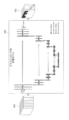
- FIG. 1 is a diagram illustrating an example of the overall configuration of the simulation system.
- FIG. 2 is a diagram illustrating an example of a hardware configuration of each device included in the simulation system.
- FIG. 3 is a diagram illustrating an example of the learning data.
- FIG. 4 is a diagram illustrating an example of a functional configuration of a learning unit of the learning device according to the first embodiment.
- FIG. 5 is a diagram illustrating an example of a functional configuration of a data shaping unit of the learning device according to the first embodiment.
- FIG. 6 is a diagram illustrating a specific example of a process performed by the data shaping unit of the learning device according to the first embodiment.
- FIG. 1 is a diagram illustrating an example of the overall configuration of the simulation system.
- FIG. 2 is a diagram illustrating an example of a hardware configuration of each device included in the simulation system.
- FIG. 3 is a diagram illustrating an example of the learning data.
- FIG. 4 is a diagram illustrating an example of a functional configuration of
- FIG. 7 is a diagram illustrating a specific example of a process using the learning model for dry etching of the learning device according to the first embodiment.
- FIG. 8 is a flowchart illustrating a flow of a learning process in the simulation system.
- FIG. 9 is a diagram illustrating an example of a functional configuration of an execution unit of the inference apparatus.
- FIG. 10 is a diagram showing the simulation accuracy of the learned model for dry etching.
- FIG. 11 is a diagram showing the simulation accuracy of the learned model for deposition.
- FIG. 12 is a diagram illustrating an example of a functional configuration of a data shaping unit of the learning device according to the second embodiment.
- FIG. 13 is a diagram illustrating a specific example of a process performed by the learning model for dry etching of the learning apparatus according to the second embodiment.
- FIG. 14 is a diagram illustrating an example of a functional configuration of a learning unit of the learning device according to the third embodiment.
- FIG. 15 is a diagram illustrating an example of a functional configuration of a data shaping unit of the learning device according to the fourth embodiment.
- FIG. 1 is a diagram illustrating an example of the overall configuration of the simulation system.
- the simulation system 100 includes a learning device 110, an inference device 120, and a simulation device 130.
- a data shaping program and a learning program are installed in the learning device 110, and the learning device 110 functions as the data shaping unit 111 and the learning unit 112 by executing the programs.
- the data shaping unit 111 is an example of a processing unit.
- the data shaping unit 111 reads the learning data transmitted from the simulation device 130 and stored in the learning data storage unit 113, and a part of the read learning data is input to the learning model by the learning unit 112. Processing into a suitable predetermined format.
- the learning unit 112 performs machine learning on the learning model using the read learning data (including the learning data processed by the data shaping unit 111), and generates a learned model of the semiconductor manufacturing process.
- the learned model generated by the learning unit 112 is provided to the inference device 120.
- a data shaping program and an execution program are installed in the inference apparatus 120, and the inference apparatus 120 functions as a data shaping unit 121 and an execution unit 122 by executing the programs.
- the data shaping unit 121 is an example of a processing unit, and acquires pre-processing image data and parameter data (details will be described later) transmitted from the simulation device 130. Further, the data shaping unit 121 processes the acquired parameter data into a predetermined format suitable for the execution unit 122 to input the learned model.
- the execution unit 122 inputs the unprocessed image data and the parameter data processed into a predetermined format in the data shaping unit 121 to the learned model, and executes the simulation to convert the processed image data (simulation result). Output (inference).
- An execution program is installed in the simulation device 130, and the simulation device 130 functions as the execution unit 131 by executing the program.
- the execution unit 131 has a simulator (a simulator based on a so-called physical model) that sets parameter data indicating predetermined processing conditions to a physical model that has identified a semiconductor manufacturing process using physical laws and the like and executes a simulation.
- the execution unit 131 reads out the unprocessed image data from the unprocessed image data storage unit 132 and executes a simulation using a simulator based on a physical model, thereby outputting the processed image data (simulation result).
- the pre-processing image data read by the execution unit 131 includes image data indicating a shape before processing of a processing target (wafer) in a semiconductor manufacturing process (for example, dry etching, deposition, or the like).
- a processing target in the semiconductor manufacturing process is composed of a plurality of materials, and each pixel of the pre-processing image data may be represented by, for example, a pixel value corresponding to the composition ratio (or content ratio) of each material. Good.
- the expression format of the pre-processing image data is not limited to this, and may be expressed in another expression format.
- the processed image data output by executing the simulation by the execution unit 131 is image data indicating a shape after dry etching when a simulator for dry etching is used.
- the processed image data output by executing the simulation by the execution unit 131 is image data indicating a shape after the deposition processing when a deposition simulator is used.
- the processing target after the processing by the semiconductor manufacturing process is also composed of a plurality of materials, and each pixel of the processed image data has, for example, a pixel value corresponding to the composition ratio (or content ratio) of each material.
- the expression format of the post-processing image data is not limited to this, and may be expressed in another expression format similarly to the pre-processing image data.
- the execution unit 131 generates learning data including pre-processing image data, corresponding parameter data, and post-processing image data used when executing the simulation, and transmits the generated learning data to the learning device 110.
- the execution unit 131 transmits the pre-processing image data, the parameter data, and the post-processing image data used by the user of the inference apparatus 120 to verify the learned model to the inference apparatus 120.
- the user of the inference apparatus 120 compares the processed image data output from the execution unit 122 by executing the simulation using the learned model with the processed image data transmitted from the execution unit 131, Verify the trained model.
- the user of the inference device 120 A simulation time in the inference apparatus 120 from the input of the pre-processing image data and the parameter data to the data shaping unit 121 to the output of the post-processing image data from the execution unit 122;
- the simulation device 130 the simulation time from when the pre-processing image data is input to the execution unit 131 to when the post-processing image data is output from the execution unit 131 with the parameter data set in the simulator based on the physical model
- the user of the inference apparatus 120 can verify whether the simulation time of the learned model is shorter than the simulation time of the simulator based on the physical model.
- the user of the inference device 120 In the inference apparatus 120, after the pre-processing image data and the parameter data are input to the data shaping section 121, the post-processing image data output from the execution section 122; In the simulation device 130, after the pre-processing image data is input to the execution unit 131 in a state where the parameter data is set in the simulator based on the physical model, the post-processing image data output from the execution unit 131; Is compared. Thereby, the user of the inference apparatus 120 can verify the simulation accuracy of the learned model with respect to the simulator based on the physical model (whether or not the simulator has simulation accuracy that can substitute for the simulator based on the physical model).
- FIG. 2 is a diagram illustrating an example of a hardware configuration of each device included in the simulation system.
- FIG. 2A is a diagram illustrating an example of a hardware configuration of the learning apparatus 110.
- the learning device 110 includes a CPU (Central Processing Unit) 201 and a ROM (Read Only Memory) 202.
- the learning device 110 has a RAM (Random Access Memory) 203 and a GPU (Graphics Processing Unit) 204.
- a processor a processing circuit, a processing circuit, a processing circuit
- a memory such as the ROM 202 and the RAM 203 form a so-called computer.
- the learning device 110 further includes an auxiliary storage device 205, an operation device 206, a display device 207, an I / F (Interface) device 208, and a drive device 209.
- the hardware of the learning device 110 is mutually connected via the bus 210.
- the CPU 201 is an arithmetic device that executes various programs (for example, a data shaping program, a learning program, and the like) installed in the auxiliary storage device 205.
- the ROM 202 is a non-volatile memory and functions as a main storage device.
- the ROM 202 stores various programs, data, and the like necessary for the CPU 201 to execute various programs installed in the auxiliary storage device 205.
- the ROM 202 stores a boot program such as BIOS (Basic Input / Output System) and EFI (Extensible Firmware Interface).
- the RAM 203 is a volatile memory such as a DRAM (Dynamic Random Access Memory) or an SRAM (Static Random Access Memory), and functions as a main storage device.
- the RAM 203 provides a work area where various programs installed in the auxiliary storage device 205 are developed when the CPU 201 executes the programs.
- the GPU 204 is an arithmetic device for image processing, and executes high-speed arithmetic by parallel processing on various image data when the CPU 201 executes various programs.
- the auxiliary storage device 205 is a storage unit that stores various programs, various image data that is subjected to image processing by the GPU 204 when the various programs are executed by the CPU 201, and the like.
- the learning data storage unit 113 is realized in the auxiliary storage device 205.
- the operation device 206 is an input device used when the administrator of the learning device 110 inputs various instructions to the learning device 110.
- the display device 207 is a display device that displays internal information of the learning device 110.
- the I / F device 208 is a connection device for connecting to and communicating with another device (for example, the simulation device 130).
- the drive device 209 is a device for setting the recording medium 220.
- the recording medium 220 includes a medium that optically, electrically, or magnetically records information, such as a CD-ROM, a flexible disk, and a magneto-optical disk.
- the recording medium 220 may include a semiconductor memory such as a ROM and a flash memory that electrically records information.
- the various programs to be installed in the auxiliary storage device 205 are installed, for example, by setting the distributed recording medium 220 to the drive device 209 and reading out the various programs recorded on the recording medium 220 by the drive device 209. Is done.
- various programs to be installed in the auxiliary storage device 205 may be installed by being downloaded via a network (not shown).
- FIG. 2B shows an example of a hardware configuration of the simulation apparatus 130. As shown in 2b of FIG. 2, the hardware configuration of the simulation device 130 is the same as the hardware configuration of the learning device 110, and a description thereof will not be repeated.
- FIG. 3 is a diagram illustrating an example of the learning data.
- the learning data 300 includes "process”, “simulation ID”, “image data before processing”, “parameter data”, and “image data after processing” as information items.
- Step 4 a name indicating a semiconductor manufacturing process is stored.
- the example of FIG. 3 shows a state in which two names “dry etching” and “deposition” are stored as “processes”.
- the “simulation ID” stores an identifier for identifying each simulation executed by the execution unit 131 using each simulator.
- the execution unit 131 has a simulator 310 for dry etching and a simulator 320 for deposition, and executes a simulation using each simulator.
- FIG. 3 shows an example in which “S001” and “S002” are stored as “simulation IDs” of the simulation executed by the execution unit 131 using the simulator 310 for dry etching. Further, the example of FIG. 3 illustrates a state in which “S101” is stored as the “simulation ID” of the simulation executed by the execution unit 131 using the deposition simulator 320.
- the "pre-processing image data” stores the file name of the pre-processing image data that is input when the execution unit 131 executes a simulation using each simulator.
- the example of FIG. 3 shows that when the simulation ID is S001, the image data before processing whose “file name” is “shape data LD001” is input to the dry etching simulator 310 to execute the simulation. Further, the example of FIG. 3 shows that when the simulation ID is S002, the image data before processing whose “file name” is “shape data LD002” is input to the simulator 310 for dry etching to execute the simulation. Further, the example of FIG. 3 shows that when the simulation ID is S101, the image data before processing whose “file name” is “shape data LD101” is input to the deposition simulator 320 to execute the simulation.
- the “parameter data” stores information indicating predetermined processing conditions set in each simulator when the execution unit 131 executes a simulation.
- the “processed image data” stores the file name of the processed image data output by the execution unit 131 executing the simulation using each simulator.
- the execution unit 131 generates learning data 300 by executing a simulation using each simulator, and transmits the learning data 300 to the learning device 110.
- the learning data storage unit 113 of the learning device 110 stores the learning data 300.
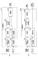
- FIG. 4 is a diagram illustrating an example of a functional configuration of a learning unit of the learning device according to the first embodiment.
- the learning unit 112 of the learning device 110 includes a learning model 420 for dry etching, a learning model 421 for deposition, a comparing unit 430, and a changing unit 440.
- the pre-processing image data and parameter data of the learning data 300 stored in the learning data storage unit 113 are read by the data shaping unit 111 and input to the corresponding learning model.
- the parameter data is processed into a predetermined format by the data shaping unit 111 and is input to the corresponding learning model.
- 111 may read and input to the corresponding learning model.
- the learning model for dry etching 420 outputs an output result.
- the learning model for dry etching 420 inputs an output result to the comparison unit 430.
- the deposition learning model 421 outputs an output result.
- the deposition learning model 421 inputs the output result to the comparison unit 430.
- the change unit 440 updates the model parameters of the dry etching learning model 420 or the deposition learning model 421 based on the difference information notified from the comparison unit 430.
- the difference information used for updating the model parameters may be a square error or an absolute error.
- the learning unit 112 inputs the pre-processing image data and the parameter data processed into a predetermined format to the learning model, and adjusts the output result output from the learning model so as to approach the processed image data. Update the model parameters by machine learning.
- FIG. 5 is a diagram illustrating an example of a functional configuration of a data shaping unit of the learning device according to the first embodiment.
- the data shaping unit 111 includes a shape data acquiring unit 501, a channel-specific data generating unit 502, a parameter data acquiring unit 511, a parameter data expanding unit 512, and a connecting unit 520.
- the shape data acquisition unit 501 reads the pre-processing image data of the learning data 300 from the learning data storage unit 113, and notifies the data-by-channel generation unit 502.
- the channel-specific data generation unit 502 is an example of a generation unit.
- the channel-specific data generation unit 502 converts the pre-processing image data (here, represented by a pixel value corresponding to the composition ratio (or content ratio) of each material) notified from the shape data acquisition unit 501. get. Further, the channel-specific data generation unit 502 generates image data of a plurality of channels according to the type of the material from the acquired pre-processing image data.
- the image data of the channel according to the type of the material is referred to as channel-specific data.
- the channel-specific data generating unit 502 generates channel-specific data including a layer of air and four channel-specific data including respective layers of four types of materials from the unprocessed image data.
- the channel-specific data generating unit 502 notifies the linking unit 520 of the plurality of generated channel-specific data.
- the channel-specific data generation unit 502 generates the channel-specific data, but the channel-specific data may be generated in advance.
- the channel-specific data generation unit 502 reads out the channel-specific data generated in advance and notifies the connection unit 520 of the read data.
- the parameter data acquisition unit 511 reads the parameter data of the learning data 300 from the learning data storage unit 113 and notifies the parameter data expanding unit 512.
- the parameter data expansion unit 512 converts the parameter data notified from the parameter data acquisition unit 511 into a predetermined format according to the image data before processing (a two-dimensional array format according to the vertical size and the horizontal size of the image data before processing). Process into
- the parameter data includes, for example, numerical values of parameters such as “parameter 001_1”, “parameter 001_2”, “parameter 001_3”,... Arranged one-dimensionally. More specifically, the parameter data is configured by one-dimensionally arranging numerical values of N types of parameters.
- the parameter data developing unit 512 extracts the values of the N types of parameters included in the parameter data one by one, and converts the extracted values into two-dimensional data according to the vertical size and the horizontal size of the image data before processing. Arrange. As a result, the parameter data developing unit 512 generates N parameter data arranged two-dimensionally.
- the parameter data expanding unit 512 notifies the linking unit 520 of the N pieces of parameter data arranged two-dimensionally.
- the connecting unit 520 connects the two-dimensionally arranged N parameter data notified from the parameter data expanding unit 512 to the plurality of channel-specific data notified from the channel-specific data generating unit 502 as a new channel. And generate linked data.
- the connection unit 520 generates the connection data, but the connection data may be generated in advance. In this case, the connection unit 520 reads out the connection data generated in advance and inputs the connection data to the learning model.
- FIG. 6 is a diagram illustrating a specific example of processing by the data shaping unit.
- the pre-processing image data 600 includes an air layer, a material A layer, a material B layer, a material C layer, and a material D layer.
- the channel-specific data generation unit 502 generates channel-specific data 601, 602, 603, 604, and 605.
- the parameter data 610 includes, for example, numerical values of respective parameters (“parameter 001_1”, “parameter 001_2”, “parameter 001_3”,%) Arranged one-dimensionally.
- the parameter data developing unit 512 arranges the parameters 001_1 two-dimensionally (the same values are arranged vertically and horizontally) according to the vertical size and the horizontal size of the image data 600 before processing. Similarly, the parameter data developing unit 512 arranges the parameters 001_2 two-dimensionally according to the vertical size and the horizontal size of the pre-processing image data 600. Similarly, the parameter data developing unit 512 arranges the parameters 001_3 two-dimensionally according to the vertical size and the horizontal size of the image data 600 before processing.
- the two-dimensionally arranged parameter data 611, 612, 613, etc. are linked by the linking unit 520 to the channel-specific data 601, 602, 603, 604, 605 as a new channel, and linked data 620 is generated.
- FIG. 7 is a diagram illustrating a specific example of a process using the learning model for dry etching of the learning device according to the first embodiment.
- a learning model (so-called UNET) based on a U-shaped convolutional neural network (CNN) is used as the learning model 420 for dry etching.
- UNET image data is normally input and image data is output. Therefore, by using the UNET as a learning model of the learning unit 112, image data before and after processing in the semiconductor manufacturing process can be input and output.
- the parameter data expanding section 512 of the data shaping section 111 is configured to arrange the parameter data two-dimensionally is to convert the data input to UNET into the image data format. Since the parameter data can be input, the simulation contents realized by the simulator based on the physical model can be realized in UNET.
- FIG. 7 shows a state in which connected data 620 is input to the learning model 420 for dry etching using UNET, and an output result 700 including a plurality of channel-specific data is output.
- FIG. 8 is a flowchart illustrating a flow of a learning process in the simulation system.
- step S801 the execution unit 131 of the simulation apparatus 130 sets parameter data in the simulator 310 for dry etching or the simulator 320 for deposition based on an instruction from the administrator of the simulation apparatus 130.
- step S802 the execution unit 131 of the simulation apparatus 130 reads out the pre-processing image data from the pre-processing image data storage unit 132.
- the execution unit 131 executes a simulation using the dry etching simulator 310 or the deposition simulator 320 (generates post-processing image data).
- step S803 the execution unit 131 of the simulation device 130 generates learning data and transmits it to the learning device 110.
- the learning data generated by the execution unit 131 includes parameter data set at the time of executing the simulation, pre-processing image data input at the time of executing the simulation, and post-processing image data generated at the time of executing the simulation.
- step S804 the data shaping unit 111 of the learning device 110 generates linked data based on the pre-processing image data and the parameter data included in the learning data.
- step S805 the learning unit 112 of the learning device 110 performs machine learning on the learning model using the connected data as input and the processed image data as output to generate a learned model.
- step S806 the learning unit 112 of the learning device 110 transmits the generated learned model to the inference device 120.
- FIG. 9 is a diagram illustrating an example of a functional configuration of the execution unit of the inference apparatus.
- the execution unit 122 of the inference apparatus 120 includes a learned model for dry etching 920, a learned model for deposition 921, and an output unit 930.
- the data shaping unit 121 When, for example, the unprocessed image data not used as the learning data 300 is transmitted from the simulation device 130 to the inference device 120 together with the parameter data, the data shaping unit 121 generates linked data. Fill in the trained model.
- “file name” “shape data SD001”, “shape data SD002”,... Are transmitted to the inference apparatus 120 as pre-processing image data not used as the learning data 300. It shows the situation.
- the learned model for dry etching 920 executes a simulation.
- the learned model for dry etching 920 notifies the output unit 930 of an output result output by executing the simulation.
- the deposition learned model 921 executes a simulation. Further, the deposition learned model 921 notifies the output unit 930 of an output result output by executing the simulation.
- the user of the inference apparatus 120 compares the time until the processed image data is output from the output unit 930 with the time until the processed image data is output from the execution unit 131, thereby performing inference.
- the simulation time of the device 120 can be verified.
- the user of the inference apparatus 120 verifies the simulation accuracy of the inference apparatus 120 by comparing the processed image data output from the output unit 930 with the processed image data output from the execution unit 131. Can be.
- the simulation time of each of the learned models of the execution unit 122 is shorter than the simulation time of each of the simulators of the execution unit 131. This is because, in the case of the simulation using each learned model, unlike the simulation using each simulator, it is not necessary to repeat the trial, and the GPU 204 can perform the high-speed operation by the parallel processing.
- each learned model of the execution unit 122 can realize a simulation accuracy that can substitute each simulator of the execution unit 131. This is because each learned model is machine-learned using the pre-processing image data and the post-processing image data input / output to / from each simulator.
- FIG. 10 is a diagram showing the simulation accuracy of the learned model for dry etching.
- reference numeral 10a in FIG. 10 indicates image data before processing and image data after processing when a simulation is performed by the dry etching simulator 310 of the simulation apparatus 130 as a comparison target.
- 10b in FIG. 10 shows the pre-processing image data and the post-processing image data when the simulation is performed by the learned model 920 for dry etching of the inference apparatus 120.
- the learned model 920 for dry etching has simulation accuracy that can substitute for the simulator 310 for dry etching.
- FIG. 11 is a diagram showing the simulation accuracy of the learned model for deposition.
- 11a in FIG. 11 shows image data before processing and image data after processing when a simulation is performed by the deposition simulator 320 of the simulation apparatus 130 as a comparison target.
- 11b in FIG. 11 shows image data before processing and image data after processing when a simulation is performed by the learned model for deposition 921 of the inference apparatus 120.
- the deposition learned model 921 has simulation accuracy that can substitute the deposition simulator 320.
- the learning device includes: Acquire pre-processing image data input to the simulator based on the physical model and parameter data set in the simulator based on the physical model.
- the obtained parameter data is processed into an image data format by arranging it two-dimensionally, and the processed parameter data is connected to the image data before processing.
- To generate consolidated data -The generated concatenated data is input to a U-shaped convolutional neural network-based learning model, and a machine is designed so that the output result output from the learning model approaches the processed image data output from a simulator based on a physical model. Do the learning.
- a learned model that realizes simulation contents realized by a simulator based on a physical model can be generated.
- the learning device of the first embodiment it is possible to generate a learned model capable of reducing the simulation time as compared with a simulator based on a physical model. Furthermore, according to the learning device according to the first embodiment, it is possible to generate a learned model having simulation accuracy that can substitute for a simulator based on a physical model.
- a simulator based on a physical model is targeted, but a simulator that is not based on a physical model can also generate a trained model similarly according to the learning device according to the first embodiment. Needless to say.
- the inference apparatus includes: -Acquire pre-processing image data and corresponding parameter data.
- the obtained parameter data is processed into an image data format by arranging it two-dimensionally, and the processed parameter data is connected to the image data before processing.
- -Input the generated connected data to the learned model generated by the learning device and execute a simulation.
- the inference apparatus it is possible to realize the simulation contents realized by the simulator based on the physical model. Further, according to the inference apparatus according to the first embodiment, the simulation time can be reduced as compared with the simulator based on the physical model, and the simulation accuracy that can substitute the simulator based on the physical model can be realized. Becomes possible.
- the simulator based on the physical model is targeted.
- the simulation content and the simulation accuracy are similarly reduced. Needless to say, this can be achieved.
- the parameter data is processed into the image data format according to the vertical size and the horizontal size of the pre-processing image data, and the processed parameter data is connected to the pre-processing image data to form a learning model (or a learned model). It has been described as input.
- the method of processing the parameter data and the method of inputting the processed parameter data to the learning model (or the learned model) are not limited to these.
- the processed parameter data may be configured to be input to each layer of the learning model (or the learned model).
- the parameter data is processed into a predetermined format used when converting the image data convolved in each layer of the learning model (or the trained model). It may be configured as follows.
- the second embodiment will be described focusing on differences from the first embodiment.
- FIG. 12 is a diagram illustrating an example of a functional configuration of a data shaping unit of the learning device according to the second embodiment.
- a difference from the functional configuration of the data shaping unit 111 illustrated in FIG. 5 is that the data shaping unit 1200 illustrated in FIG. 12 includes a connecting unit 1201 and a normalizing unit 1202.
- the linking unit 1201 links the plurality of channel-specific data notified from the channel-specific data generating unit 502 to generate linked data.
- the normalization unit 1202 normalizes the parameter data notified from the parameter data acquisition unit 511, and generates normalized parameter data.
- FIG. 13 is a diagram illustrating a specific example of a process performed by the learning model for dry etching of the learning apparatus according to the second embodiment.
- connection data 1310 generated by the connection unit 1201 of the data shaping unit 1200 is input to the learning model for dry etching 1300.
- the normalization parameter data generated by the normalization unit 1202 of the data shaping unit 1200 is input to the learning model 1300 for dry etching. You.
- the learning model for dry etching 1300 includes a neural network unit 1301, which is a fully-coupled learning model, in addition to UNET, which is a CNN-based learning model.
- the neural network unit 1301 converts a value of a predetermined format (for example, a linear expression) used when converting the value of each pixel of each image data on which convolution processing is performed in each layer of UNET. ⁇ , ⁇ ) are output. That is, the neural network unit 1301 has a function of processing the normalized parameter data into a predetermined format (for example, a linear coefficient format).
- a predetermined format for example, a linear expression
- the neural network unit 1301 outputs ( ⁇ 1 , ⁇ 1 ) to ( ⁇ 9 , ⁇ 9 ) as coefficients of a linear expression.
- the coefficient of the linear equation is input to each layer for each data for each channel. It is assumed that a plurality of sets are input.
- the coefficients ( ⁇ 1 , ⁇ 1 ) to ( ⁇ 9 , ⁇ 9 ) of the linear expression are, for example, any of the image data among the image data for each channel for which the convolution processing is performed in each layer of the UNET. It can be considered as an indicator that data is important. That is, the neural network unit 1301 performs a process of calculating an index indicating the importance of each image data processed in each layer of the learning model based on the normalized parameter data.
- an output result 700 including a plurality of channel-specific data is output.
- the output result 700 is compared with the processed image data by the comparing unit 430, and difference information is calculated.
- the changing unit 440 updates the model parameters of the UNET and the model parameters of the neural network unit 1301 in the learning model for dry etching 1300 based on the difference information.
- image data having a high importance in each layer of the UNET is determined based on the normalized parameter data. It becomes possible to extract.
- the learning device includes: Acquire pre-processing image data input to the simulator based on the physical model and parameter data set in the simulator based on the physical model. Normalize the acquired parameter data and process it into the form of linear coefficients used when converting the value of each pixel of each image data to be convolved in each layer of the learning model.
- the learning unit performs machine learning, the value of each pixel of the image data convolved in each layer is converted using a linear expression.
- a learned model that realizes simulation contents realized by a simulator based on a physical model can be generated.
- the learning device of the second embodiment it is possible to generate a learned model capable of reducing the simulation time as compared with a simulator based on a physical model. Furthermore, according to the learning device according to the second embodiment, it is possible to generate a learned model having simulation accuracy that can substitute for a simulator based on a physical model.
- the learning device has been described in the second embodiment, the same processing is performed in the inference device when the execution unit executes the simulation.
- FIG. 14 is a diagram illustrating an example of a functional configuration of a learning unit of the learning device according to the third embodiment.
- the internal configuration in the learning model is different from the functional configuration of the learning unit 112 illustrated in FIG.
- the internal structure in the learning model will be described using the learning model for dry etching 1410, but the learning model for deposition also has the same internal structure.
- the learning model for dry etching 1410 of the learning unit 1400 includes a sigmoid function unit 1412 and a multiplication unit 1413 in addition to the UNET 1411.
- the sigmoid function unit 1412 is an example of a processing unit. As shown in FIG. 14, the sigmoid function unit 1412 multiplies a first output result output from the UNET 1411 by a sigmoid function 1420 to output a second output result 1421.
- the multiplication unit 1413 obtains the second output result 1421 from the sigmoid function unit 1412. Further, the multiplying unit 1413 acquires the unprocessed image data from the data shaping unit 111. Further, the multiplying unit 1413 notifies the comparing unit 430 of the final output result 1422 by multiplying the obtained image data before processing by the obtained second output result 1421.
- the UNET 1411 in the case where the learning model for dry etching 1410 is machine-learned is used as the first output result as the first output result. Is output.
- the scraping rate refers to a value of a change rate indicating how much each material layer included in the pre-processing image data has been cut in the post-processing image data.
- the shaving rate approaches a value obtained by dividing the image data after processing by the image data before processing.
- the first output result output from the UNET 1411 in the process of machine learning takes an arbitrary value.
- the sigmoid function unit 1412 is a function for converting an arbitrary value to a value of 0 to 1.
- the sigmoid function unit 1412 converts the first output result to a second output result, thereby obtaining the domain knowledge. Can be reflected.
- image data indicating the adhesion rate is output as the first output result from UNET when the learning model for deposition is machine-learned.
- the adhesion rate refers to a value of a change rate indicating how much a thin film adheres to the layer of each material included in the image data before processing in the image data after processing.
- the adhesion rate approaches a value obtained by dividing the difference between the image data before processing and the image data after processing by the image data before processing.
- the first output result output from UNET in the process of machine learning takes an arbitrary value.
- the adhesion rate falls within the range of 0 to 1.
- the sigmoid function unit is a function that converts an arbitrary value into a value of 0 to 1.
- the sigmoid function unit converts the first output result into the second output result, thereby reflecting the domain knowledge. Can be done.
- the domain knowledge can be reflected in the machine learning, and the simulation accuracy can be further improved.
- the data shaping unit has been described as generating the linked data of the vertical size and the horizontal size according to the vertical size and the horizontal size of the image data before processing.
- the vertical size and the horizontal size of the concatenated data generated by the data shaping unit are arbitrary, and the concatenated data may be generated after compressing the image data before processing.
- the fourth embodiment will be described focusing on differences from the first to third embodiments.
- FIG. 15 is a diagram illustrating an example of a functional configuration of a data shaping unit of the learning device according to the fourth embodiment.
- 15a of FIG. 15 shows a data shaping unit 1510 in which a compression unit 1511 is added to the data shaping unit 111 of the learning device according to the first embodiment.
- the compression unit 1511 compresses the pre-processing image data acquired by the shape data acquisition unit 501.
- the obtained average value is defined as the pixel value of one pixel obtained by combining the n pixels.
- the compression unit 1511 can compress the unprocessed image data by a factor of 1 / n.
- the compression unit 1511 performs the composition ratio (or content ratio) of the material before and after compression. Compression processing is performed so that is maintained as much as possible. Note that the compression rate of the compression process by the compression unit 1511 is not limited to an integral multiple, and the compression unit 1511 can perform compression processing at an arbitrary compression ratio.
- 15b in FIG. 15 shows a data shaping unit 1520 obtained by adding a compression unit 1511 to the data shaping unit 1200 of the learning device according to the second embodiment.
- the compression unit 1511 of the data shaping unit 1520 has the same function as the compression unit 1511 of the data shaping unit 1510. Therefore, a detailed description is omitted here.
- the size of the concatenated data input to the learning units 112 and 1400 (or the execution unit 122) can be reduced.
- the learning time when the learning units 112 and 1400 perform machine learning, or the simulation time when the execution unit 122 executes a simulation can be reduced.
- the learning unit 112 is provided with the learning model 420 for dry etching and the learning model 421 for deposition, and machine learning is performed separately using different learning data.
- dry etching and deposition may occur simultaneously.
- one learning model may be provided in the learning unit 112 so that machine learning is performed for a case where dry etching and deposition occur simultaneously.
- the learning unit 112 includes, for the one learning model, a learning model including pre-processing image data before dry etching and deposition occurs and post-processing image data after dry etching and deposition occurs. Perform machine learning using data.
- the learning unit 112 of the learning device 110 integrates the learning models. Can also.
- the image data before processing and the image data after processing are described as two-dimensional image data.
- the image data before processing and the image data after processing are not limited to two-dimensional image data, but may be three-dimensional image data (so-called voxel data).
- the concatenated data When the pre-processing image data is two-dimensional image data, the concatenated data has an array of (channel, vertical size, horizontal size). However, when the pre-processing image data is three-dimensional image data, the concatenated data is , (Channel, vertical size, horizontal size, depth size).
- the two-dimensional image data is deformed or the three-dimensional image data is deformed and handled.
- three-dimensional image data may be acquired, two-dimensional image data of a predetermined cross section may be generated, and input as pre-processing image data.
- three-dimensional image data may be generated based on two-dimensional image data of a continuous predetermined cross section and input as pre-processing image data.
- the method of generating the data for each channel is not limited to this, and the data for each channel is generated based on a larger classification such as Oxide, Silicon, Organics, and Nitride instead of each specific film type. Is also good.
- the inference apparatus 120 outputs the post-processing image data and ends the processing when the pre-processing image data and the parameter data are input.
- the configuration of the inference apparatus 120 is not limited to this.
- the pre-processing image data and the post-processing image data output by inputting the parameter data are transmitted to the inference apparatus 120 again together with the corresponding parameter data. You may comprise so that it may input.
- the inference device 120 can continuously output a change in shape.
- the processed image data is input to the inference apparatus 120 again, it is assumed that the corresponding parameter data can be arbitrarily changed.
- the learning device 110, the inference device 120, and the simulation device 130 are shown as separate units, but any two devices may be integrally configured. , All the devices may be configured integrally.
- the learning device 110 has been described as being configured with one computer, but may be configured with a plurality of computers.
- the inference apparatus 120 has been described as being configured by one computer, but may be configured by a plurality of computers.
- the learning device 110, the inference device 120, and the simulation device 130 have been described as being applied to the semiconductor manufacturing process. Needless to say, it is good.
- the processes other than the semiconductor manufacturing process include manufacturing processes other than the semiconductor manufacturing process and non-manufacturing processes.
- the learning device 110 and the inference device 120 are realized by causing a general-purpose computer to execute various programs. Not limited.
- a dedicated electronic circuit that is, hardware
- IC Integrated Circuit
- a plurality of components may be realized by one electronic circuit, one component may be realized by a plurality of electronic circuits, or one component and one electronic circuit may be realized.
- the present invention is not limited to the configuration shown here, such as a combination of the configuration described in the above embodiment with other elements. These points can be changed without departing from the spirit of the present invention, and can be appropriately determined according to the application form.
Landscapes
- Engineering & Computer Science (AREA)
- Chemical & Material Sciences (AREA)
- Theoretical Computer Science (AREA)
- Physics & Mathematics (AREA)
- Software Systems (AREA)
- General Physics & Mathematics (AREA)
- Computing Systems (AREA)
- Artificial Intelligence (AREA)
- Mathematical Physics (AREA)
- Data Mining & Analysis (AREA)
- Evolutionary Computation (AREA)
- General Engineering & Computer Science (AREA)
- Computational Linguistics (AREA)
- Molecular Biology (AREA)
- General Health & Medical Sciences (AREA)
- Biophysics (AREA)
- Biomedical Technology (AREA)
- Life Sciences & Earth Sciences (AREA)
- Health & Medical Sciences (AREA)
- Materials Engineering (AREA)
- Chemical Kinetics & Catalysis (AREA)
- Mechanical Engineering (AREA)
- Metallurgy (AREA)
- Organic Chemistry (AREA)
- Computer Vision & Pattern Recognition (AREA)
- General Chemical & Material Sciences (AREA)
- Quality & Reliability (AREA)
- Medical Informatics (AREA)
- Drying Of Semiconductors (AREA)
- Image Analysis (AREA)
Abstract
Priority Applications (4)
| Application Number | Priority Date | Filing Date | Title |
|---|---|---|---|
| JP2020503074A JP6724267B1 (ja) | 2018-09-03 | 2019-08-15 | 学習装置、推論装置、学習モデルの生成方法及び推論方法 |
| KR1020217006384A KR102513707B1 (ko) | 2018-09-03 | 2019-08-15 | 학습 장치, 추론 장치, 학습 모델 생성 방법 및 추론 방법 |
| CN201980057325.4A CN112640037A (zh) | 2018-09-03 | 2019-08-15 | 学习装置、推理装置、学习模型的生成方法及推理方法 |
| US17/189,592 US12033311B2 (en) | 2018-09-03 | 2021-03-02 | Learning device, inference device, learning model generation method, and inference method |
Applications Claiming Priority (2)
| Application Number | Priority Date | Filing Date | Title |
|---|---|---|---|
| JP2018164930 | 2018-09-03 | ||
| JP2018-164930 | 2018-09-03 |
Related Child Applications (1)
| Application Number | Title | Priority Date | Filing Date |
|---|---|---|---|
| US17/189,592 Continuation US12033311B2 (en) | 2018-09-03 | 2021-03-02 | Learning device, inference device, learning model generation method, and inference method |
Publications (1)
| Publication Number | Publication Date |
|---|---|
| WO2020049974A1 true WO2020049974A1 (fr) | 2020-03-12 |
Family
ID=69722906
Family Applications (1)
| Application Number | Title | Priority Date | Filing Date |
|---|---|---|---|
| PCT/JP2019/032025 Ceased WO2020049974A1 (fr) | 2018-09-03 | 2019-08-15 | Dispositif d'apprentissage, dispositif d'inférence, procédé de génération de modèle d'apprentissage et procédé d'inférence |
Country Status (6)
| Country | Link |
|---|---|
| US (1) | US12033311B2 (fr) |
| JP (2) | JP6724267B1 (fr) |
| KR (1) | KR102513707B1 (fr) |
| CN (1) | CN112640037A (fr) |
| TW (1) | TWI840403B (fr) |
| WO (1) | WO2020049974A1 (fr) |
Cited By (8)
| Publication number | Priority date | Publication date | Assignee | Title |
|---|---|---|---|---|
| WO2022145225A1 (fr) * | 2020-12-28 | 2022-07-07 | 東京エレクトロン株式会社 | Appareil de déduction de paramètre, procédé de déduction de paramètre et programme de déduction de paramètre |
| KR20230042643A (ko) | 2021-09-22 | 2023-03-29 | 가부시키가이샤 스크린 홀딩스 | 학습 장치, 정보 처리 장치, 기판 처리 장치, 기판 처리 시스템, 학습 방법, 레시피 결정 방법 및 학습 프로그램 |
| WO2023058688A1 (fr) * | 2021-10-08 | 2023-04-13 | 東京エレクトロン株式会社 | Système de processus de gravure, procédé de prédiction de qualité de gravure et système de prédiction de qualité de gravure |
| JP2023120961A (ja) * | 2022-02-18 | 2023-08-30 | 株式会社Screenホールディングス | 基板処理条件の設定方法、基板処理方法、基板処理条件の設定システム、及び、基板処理システム |
| JP2023540529A (ja) * | 2020-09-07 | 2023-09-25 | ケーエルエー コーポレイション | マイクロ電子デバイス製造中に物理的シミュレーションモデルを加速するシステムおよび方法 |
| WO2024005047A1 (fr) * | 2022-07-01 | 2024-01-04 | 東京エレクトロン株式会社 | Procédé de commande de dispositif de traitement de substrat et système de traitement de substrat |
| WO2024070233A1 (fr) * | 2022-09-26 | 2024-04-04 | 株式会社Screenホールディングス | Dispositif d'apprentissage, dispositif de traitement d'informations, dispositif de traitement de substrat, système de traitement de substrat, procédé d'apprentissage et procédé de détermination de conditions de traitement |
| JP7704275B1 (ja) * | 2024-09-25 | 2025-07-08 | Agc株式会社 | 半導体装置設計システム、半導体装置の設計方法、及びプログラム |
Families Citing this family (6)
| Publication number | Priority date | Publication date | Assignee | Title |
|---|---|---|---|---|
| JP2021111066A (ja) * | 2020-01-08 | 2021-08-02 | 株式会社科学計算総合研究所 | 情報処理システム、情報処理方法及びプログラム |
| US12450520B2 (en) | 2021-03-01 | 2025-10-21 | Hitachi High-Tech Corporation | Experiment point recommendation device, experiment point recommendation method, and semiconductor device manufacturing device |
| JP7722793B2 (ja) * | 2021-05-14 | 2025-08-13 | 東京エレクトロン株式会社 | 評価装置、評価方法及び評価プログラム |
| JP7797149B2 (ja) * | 2021-09-22 | 2026-01-13 | キヤノン株式会社 | 解析方法 |
| US12468998B2 (en) * | 2021-11-12 | 2025-11-11 | Starbucks Corporation | System for configuring an environment based on modifications to simulated virtual environments |
| CN118235455A (zh) * | 2021-11-15 | 2024-06-21 | Oppo广东移动通信有限公司 | 用于无线信道处理的模型更新方法、装置、终端及介质 |
Citations (11)
| Publication number | Priority date | Publication date | Assignee | Title |
|---|---|---|---|---|
| JPH06224126A (ja) * | 1993-01-25 | 1994-08-12 | Fuji Electric Co Ltd | 半導体製造装置の膜質予測装置 |
| JPH11330449A (ja) * | 1998-05-20 | 1999-11-30 | Toshiba Corp | 半導体装置の製造方法、シミュレーション装置、シミュレーション方法、シミュレーションプログラムを記録した記録媒体、及びシミュレーション用データを記録した記録媒体 |
| JP2004040004A (ja) * | 2002-07-08 | 2004-02-05 | Renesas Technology Corp | 配線設計データを利用した化学的機械的研磨方法、加工物の製造方法、およびデザインルール決定方法 |
| JP2004153229A (ja) * | 2002-03-14 | 2004-05-27 | Nikon Corp | 加工形状の予測方法、加工条件の決定方法、加工量予測方法、加工形状予測システム、加工条件決定システム、加工システム、加工形状予測計算機プログラム、加工条件決定計算機プログラム、プログラム記録媒体、及び半導体デバイスの製造方法 |
| JP2007507888A (ja) * | 2003-09-30 | 2007-03-29 | 東京エレクトロン株式会社 | 半導体製造プロセスを制御するために第1の原理シミュレーションを用いたシステム及び方法。 |
| JP2007227618A (ja) * | 2006-02-23 | 2007-09-06 | Hitachi High-Technologies Corp | 半導体プロセスモニタ方法およびそのシステム |
| JP2010079896A (ja) * | 2008-09-25 | 2010-04-08 | Internatl Business Mach Corp <Ibm> | 集積回路設計中の製造の影響の高速シミュレーションを行なうための装置、方法及びコンピュータ・プログラム |
| JP2011071296A (ja) * | 2009-09-25 | 2011-04-07 | Sharp Corp | 特性予測装置、特性予測方法、特性予測プログラムおよびプログラム記録媒体 |
| JP2013518449A (ja) * | 2010-01-29 | 2013-05-20 | 東京エレクトロン株式会社 | 半導体製造ツールを自己学習及び自己改善するための方法及びシステム |
| US20170194126A1 (en) * | 2015-12-31 | 2017-07-06 | Kla-Tencor Corporation | Hybrid inspectors |
| JP2018049936A (ja) * | 2016-09-21 | 2018-03-29 | 株式会社日立製作所 | 探索装置および探索方法 |
Family Cites Families (21)
| Publication number | Priority date | Publication date | Assignee | Title |
|---|---|---|---|---|
| KR20020085688A (ko) | 2001-05-09 | 2002-11-16 | 학교법인 인하학원 | 반도체 식각 공정 모의 실험 해석기 및 해석 방법 |
| US6819427B1 (en) * | 2001-10-10 | 2004-11-16 | Advanced Micro Devices, Inc. | Apparatus of monitoring and optimizing the development of a photoresist material |
| TW592300U (en) * | 2003-01-29 | 2004-06-11 | Midway Elecpronics Co Ltd | Electric meter calibrating device using common memory to transfer calibrating parameters |
| KR20040080742A (ko) | 2003-03-13 | 2004-09-20 | 원태영 | 식각 공정 시뮬레이션의 병렬 연산 구현 방법 |
| JP2005202949A (ja) | 2003-12-01 | 2005-07-28 | Oscillated Recall Technology:Kk | 大域的エッチングシミュレータ |
| US8722547B2 (en) * | 2006-04-20 | 2014-05-13 | Applied Materials, Inc. | Etching high K dielectrics with high selectivity to oxide containing layers at elevated temperatures with BC13 based etch chemistries |
| US9245714B2 (en) * | 2012-10-01 | 2016-01-26 | Kla-Tencor Corporation | System and method for compressed data transmission in a maskless lithography system |
| JP6173889B2 (ja) | 2013-11-28 | 2017-08-02 | ソニーセミコンダクタソリューションズ株式会社 | シミュレーション方法、シミュレーションプログラム、加工制御システム、シミュレータ、プロセス設計方法およびマスク設計方法 |
| JP2016071597A (ja) * | 2014-09-30 | 2016-05-09 | ソニー株式会社 | 情報処理装置、情報処理方法及びプログラム |
| US10056304B2 (en) * | 2014-11-19 | 2018-08-21 | Deca Technologies Inc | Automated optical inspection of unit specific patterning |
| US9965901B2 (en) | 2015-11-19 | 2018-05-08 | KLA—Tencor Corp. | Generating simulated images from design information |
| IL259633B (en) * | 2015-12-22 | 2022-07-01 | Asml Netherlands Bv | A device and method for characterizing a window process |
| WO2017117568A1 (fr) * | 2015-12-31 | 2017-07-06 | Kla-Tencor Corporation | Formation accélérée d'un modèle fondé sur l'apprentissage automatique destiné à des applications semi-conductrices |
| JP2017182129A (ja) | 2016-03-28 | 2017-10-05 | ソニー株式会社 | 情報処理装置。 |
| JP6635476B2 (ja) * | 2017-08-09 | 2020-01-29 | 学校法人東京女子医科大学 | 線量分布予測システム、線量分布予測方法及び線量分布予測プログラム |
| JP6768946B2 (ja) * | 2017-10-17 | 2020-10-14 | 株式会社アルバック | 被処理体の処理装置 |
| CN107909114B (zh) * | 2017-11-30 | 2020-07-17 | 深圳地平线机器人科技有限公司 | 训练有监督机器学习的模型的方法和装置 |
| CN107945175A (zh) * | 2017-12-12 | 2018-04-20 | 百度在线网络技术(北京)有限公司 | 图像的评价方法、装置、服务器及存储介质 |
| US11199506B2 (en) * | 2018-02-21 | 2021-12-14 | Applied Materials Israel Ltd. | Generating a training set usable for examination of a semiconductor specimen |
| US10572697B2 (en) * | 2018-04-06 | 2020-02-25 | Lam Research Corporation | Method of etch model calibration using optical scatterometry |
| JP2019219756A (ja) * | 2018-06-15 | 2019-12-26 | 国立研究開発法人理化学研究所 | 制御装置、制御方法、プログラム、ならびに、情報記録媒体 |
-
2019
- 2019-08-15 WO PCT/JP2019/032025 patent/WO2020049974A1/fr not_active Ceased
- 2019-08-15 KR KR1020217006384A patent/KR102513707B1/ko active Active
- 2019-08-15 CN CN201980057325.4A patent/CN112640037A/zh active Pending
- 2019-08-15 JP JP2020503074A patent/JP6724267B1/ja active Active
- 2019-08-28 TW TW108130789A patent/TWI840403B/zh active
-
2020
- 2020-06-24 JP JP2020108905A patent/JP7291670B2/ja active Active
-
2021
- 2021-03-02 US US17/189,592 patent/US12033311B2/en active Active
Patent Citations (11)
| Publication number | Priority date | Publication date | Assignee | Title |
|---|---|---|---|---|
| JPH06224126A (ja) * | 1993-01-25 | 1994-08-12 | Fuji Electric Co Ltd | 半導体製造装置の膜質予測装置 |
| JPH11330449A (ja) * | 1998-05-20 | 1999-11-30 | Toshiba Corp | 半導体装置の製造方法、シミュレーション装置、シミュレーション方法、シミュレーションプログラムを記録した記録媒体、及びシミュレーション用データを記録した記録媒体 |
| JP2004153229A (ja) * | 2002-03-14 | 2004-05-27 | Nikon Corp | 加工形状の予測方法、加工条件の決定方法、加工量予測方法、加工形状予測システム、加工条件決定システム、加工システム、加工形状予測計算機プログラム、加工条件決定計算機プログラム、プログラム記録媒体、及び半導体デバイスの製造方法 |
| JP2004040004A (ja) * | 2002-07-08 | 2004-02-05 | Renesas Technology Corp | 配線設計データを利用した化学的機械的研磨方法、加工物の製造方法、およびデザインルール決定方法 |
| JP2007507888A (ja) * | 2003-09-30 | 2007-03-29 | 東京エレクトロン株式会社 | 半導体製造プロセスを制御するために第1の原理シミュレーションを用いたシステム及び方法。 |
| JP2007227618A (ja) * | 2006-02-23 | 2007-09-06 | Hitachi High-Technologies Corp | 半導体プロセスモニタ方法およびそのシステム |
| JP2010079896A (ja) * | 2008-09-25 | 2010-04-08 | Internatl Business Mach Corp <Ibm> | 集積回路設計中の製造の影響の高速シミュレーションを行なうための装置、方法及びコンピュータ・プログラム |
| JP2011071296A (ja) * | 2009-09-25 | 2011-04-07 | Sharp Corp | 特性予測装置、特性予測方法、特性予測プログラムおよびプログラム記録媒体 |
| JP2013518449A (ja) * | 2010-01-29 | 2013-05-20 | 東京エレクトロン株式会社 | 半導体製造ツールを自己学習及び自己改善するための方法及びシステム |
| US20170194126A1 (en) * | 2015-12-31 | 2017-07-06 | Kla-Tencor Corporation | Hybrid inspectors |
| JP2018049936A (ja) * | 2016-09-21 | 2018-03-29 | 株式会社日立製作所 | 探索装置および探索方法 |
Cited By (18)
| Publication number | Priority date | Publication date | Assignee | Title |
|---|---|---|---|---|
| JP7821784B2 (ja) | 2020-09-07 | 2026-02-27 | ケーエルエー コーポレイション | マイクロ電子デバイス製造中に物理的シミュレーションモデルを加速するシステムおよび方法 |
| JP2023540529A (ja) * | 2020-09-07 | 2023-09-25 | ケーエルエー コーポレイション | マイクロ電子デバイス製造中に物理的シミュレーションモデルを加速するシステムおよび方法 |
| JPWO2022145225A1 (fr) * | 2020-12-28 | 2022-07-07 | ||
| WO2022145225A1 (fr) * | 2020-12-28 | 2022-07-07 | 東京エレクトロン株式会社 | Appareil de déduction de paramètre, procédé de déduction de paramètre et programme de déduction de paramètre |
| JP7540872B2 (ja) | 2020-12-28 | 2024-08-27 | 東京エレクトロン株式会社 | パラメータ導出装置、パラメータ導出方法及びパラメータ導出プログラム |
| KR20230042643A (ko) | 2021-09-22 | 2023-03-29 | 가부시키가이샤 스크린 홀딩스 | 학습 장치, 정보 처리 장치, 기판 처리 장치, 기판 처리 시스템, 학습 방법, 레시피 결정 방법 및 학습 프로그램 |
| US12475386B2 (en) | 2021-09-22 | 2025-11-18 | SCREEN Holdings Co., Ltd. | Learning device, information processing apparatus, substrate processing device, substrate processing system, learning method, recipe determination method and non-transitory computer-readable medium storing learning program |
| JP7701128B2 (ja) | 2021-10-08 | 2025-07-01 | 東京エレクトロン株式会社 | エッチング処理システム、エッチング品質予測方法及びエッチング品質予測プログラム |
| WO2023058688A1 (fr) * | 2021-10-08 | 2023-04-13 | 東京エレクトロン株式会社 | Système de processus de gravure, procédé de prédiction de qualité de gravure et système de prédiction de qualité de gravure |
| JP2023056708A (ja) * | 2021-10-08 | 2023-04-20 | 東京エレクトロン株式会社 | エッチング処理システム、エッチング品質予測方法及びエッチング品質予測プログラム |
| JP7709930B2 (ja) | 2022-02-18 | 2025-07-17 | 株式会社Screenホールディングス | 基板処理条件の設定方法、基板処理方法、基板処理条件の設定システム、及び、基板処理システム |
| US12476124B2 (en) | 2022-02-18 | 2025-11-18 | SCREEN Holdings Co., Ltd. | Substrate processing condition setting method, substrate processing method, substrate processing condition setting system, and substrate processing system |
| JP2023120961A (ja) * | 2022-02-18 | 2023-08-30 | 株式会社Screenホールディングス | 基板処理条件の設定方法、基板処理方法、基板処理条件の設定システム、及び、基板処理システム |
| WO2024005047A1 (fr) * | 2022-07-01 | 2024-01-04 | 東京エレクトロン株式会社 | Procédé de commande de dispositif de traitement de substrat et système de traitement de substrat |
| WO2024070233A1 (fr) * | 2022-09-26 | 2024-04-04 | 株式会社Screenホールディングス | Dispositif d'apprentissage, dispositif de traitement d'informations, dispositif de traitement de substrat, système de traitement de substrat, procédé d'apprentissage et procédé de détermination de conditions de traitement |
| TWI891045B (zh) * | 2022-09-26 | 2025-07-21 | 日商斯庫林集團股份有限公司 | 學習裝置、資訊處理裝置、基板處理裝置、基板處理系統、學習方法及處理條件決定方法 |
| JP7704275B1 (ja) * | 2024-09-25 | 2025-07-08 | Agc株式会社 | 半導体装置設計システム、半導体装置の設計方法、及びプログラム |
| WO2026069860A1 (fr) * | 2024-09-25 | 2026-04-02 | Agc株式会社 | Système de conception de dispositif à semi-conducteur, procédé de conception de dispositif à semi-conducteur et programme |
Also Published As
| Publication number | Publication date |
|---|---|
| TW202024377A (zh) | 2020-07-01 |
| US20210183051A1 (en) | 2021-06-17 |
| CN112640037A (zh) | 2021-04-09 |
| JP2020191096A (ja) | 2020-11-26 |
| TWI840403B (zh) | 2024-05-01 |
| KR102513707B1 (ko) | 2023-03-23 |
| KR20210036391A (ko) | 2021-04-02 |
| US12033311B2 (en) | 2024-07-09 |
| JP7291670B2 (ja) | 2023-06-15 |
| JP6724267B1 (ja) | 2020-07-15 |
| JPWO2020049974A1 (ja) | 2020-09-10 |
Similar Documents
| Publication | Publication Date | Title |
|---|---|---|
| WO2020049974A1 (fr) | Dispositif d'apprentissage, dispositif d'inférence, procédé de génération de modèle d'apprentissage et procédé d'inférence | |
| JP7190495B2 (ja) | 推論方法、推論装置、モデルの生成方法及び学習装置 | |
| JP2020057172A (ja) | 学習装置、推論装置及び学習済みモデル | |
| WO2020166278A1 (fr) | Système, dispositif d'entraînement, procédé d'entraînement, et dispositif de prédiction | |
| US20230136021A1 (en) | Method and system for three-dimensional modeling | |
| US11676030B2 (en) | Learning method, learning apparatus, and computer-readable recording medium | |
| US11900514B2 (en) | Digital content editing using a procedural model | |
| CN115034351B (zh) | 数据处理方法、卷积神经网络训练方法、装置和fpga | |
| CN116957018A (zh) | 一种逐通道卷积的实现方法 | |
| CN120144258A (zh) | 神经网络模型的运行方法、芯片、电子设备及存储介质 | |
| CN114842312B (zh) | 面向不配对跨模态图像分割模型的生成及分割方法、装置 | |
| US10650581B1 (en) | Sketch-based 3D fluid volume generation using a machine learning system | |
| JP7852576B2 (ja) | 情報処理装置、情報処理方法及び情報処理プログラム | |
| JP6633267B2 (ja) | 次元削減装置、方法及びプログラム | |
| JP7666645B2 (ja) | 情報処理装置、情報処理方法、及び記録媒体 | |
| US20240202910A1 (en) | Method and apparatus with semiconductor image processing | |
| JP2025124319A (ja) | モデル生成装置、モデル生成方法、及びプログラム | |
| JP2024172967A (ja) | 情報処理装置、情報処理方法及び情報処理プログラム | |
| JP2026051752A (ja) | 情報処理装置、情報処理方法およびプログラム | |
| WO2025134819A1 (fr) | Procédé d'entraînement et dispositif d'entraînement | |
| WO2026053443A1 (fr) | Dispositif de visualisation et procédé de visualisation | |
| JP2025013037A (ja) | 量子情報処理方法、量子情報処理プログラム、古典コンピュータ、及びハイブリッドシステム | |
| CN121599833A (zh) | 基于二维卷积和动态权重的俯视特征图提取方法及系统 | |
| JP2022045087A (ja) | モデル解析装置、モデル解析方法、及びプログラム |
Legal Events
| Date | Code | Title | Description |
|---|---|---|---|
| ENP | Entry into the national phase |
Ref document number: 2020503074 Country of ref document: JP Kind code of ref document: A |
|
| 121 | Ep: the epo has been informed by wipo that ep was designated in this application |
Ref document number: 19856899 Country of ref document: EP Kind code of ref document: A1 |
|
| ENP | Entry into the national phase |
Ref document number: 20217006384 Country of ref document: KR Kind code of ref document: A |
|
| NENP | Non-entry into the national phase |
Ref country code: DE |
|
| 122 | Ep: pct application non-entry in european phase |
Ref document number: 19856899 Country of ref document: EP Kind code of ref document: A1 |