WO2020079959A1 - Corps lié et élément à ondes acoustiques - Google Patents
Corps lié et élément à ondes acoustiques Download PDFInfo
- Publication number
- WO2020079959A1 WO2020079959A1 PCT/JP2019/033130 JP2019033130W WO2020079959A1 WO 2020079959 A1 WO2020079959 A1 WO 2020079959A1 JP 2019033130 W JP2019033130 W JP 2019033130W WO 2020079959 A1 WO2020079959 A1 WO 2020079959A1
- Authority
- WO
- WIPO (PCT)
- Prior art keywords
- bonding layer
- layer
- ratio
- substrate
- piezoelectric material
- Prior art date
- Legal status (The legal status is an assumption and is not a legal conclusion. Google has not performed a legal analysis and makes no representation as to the accuracy of the status listed.)
- Ceased
Links
Images
Classifications
-
- H—ELECTRICITY
- H10—SEMICONDUCTOR DEVICES; ELECTRIC SOLID-STATE DEVICES NOT OTHERWISE PROVIDED FOR
- H10N—ELECTRIC SOLID-STATE DEVICES NOT OTHERWISE PROVIDED FOR
- H10N30/00—Piezoelectric or electrostrictive devices
- H10N30/01—Manufacture or treatment
- H10N30/07—Forming of piezoelectric or electrostrictive parts or bodies on an electrical element or another base
- H10N30/072—Forming of piezoelectric or electrostrictive parts or bodies on an electrical element or another base by laminating or bonding of piezoelectric or electrostrictive bodies
- H10N30/073—Forming of piezoelectric or electrostrictive parts or bodies on an electrical element or another base by laminating or bonding of piezoelectric or electrostrictive bodies by fusion of metals or by adhesives
-
- H—ELECTRICITY
- H03—ELECTRONIC CIRCUITRY
- H03H—IMPEDANCE NETWORKS, e.g. RESONANT CIRCUITS; RESONATORS
- H03H9/00—Networks comprising electromechanical or electro-acoustic elements; Electromechanical resonators
- H03H9/02—Details
- H03H9/02535—Details of surface acoustic wave devices
- H03H9/02543—Characteristics of substrate, e.g. cutting angles
- H03H9/02574—Characteristics of substrate, e.g. cutting angles of combined substrates, multilayered substrates, piezoelectrical layers on not-piezoelectrical substrate
-
- H—ELECTRICITY
- H03—ELECTRONIC CIRCUITRY
- H03H—IMPEDANCE NETWORKS, e.g. RESONANT CIRCUITS; RESONATORS
- H03H3/00—Apparatus or processes specially adapted for the manufacture of impedance networks, resonating circuits, resonators
- H03H3/007—Apparatus or processes specially adapted for the manufacture of impedance networks, resonating circuits, resonators for the manufacture of electromechanical resonators or networks
- H03H3/08—Apparatus or processes specially adapted for the manufacture of impedance networks, resonating circuits, resonators for the manufacture of electromechanical resonators or networks for the manufacture of resonators or networks using surface acoustic waves
-
- H—ELECTRICITY
- H03—ELECTRONIC CIRCUITRY
- H03H—IMPEDANCE NETWORKS, e.g. RESONANT CIRCUITS; RESONATORS
- H03H9/00—Networks comprising electromechanical or electro-acoustic elements; Electromechanical resonators
- H03H9/02—Details
- H03H9/02535—Details of surface acoustic wave devices
- H03H9/02543—Characteristics of substrate, e.g. cutting angles
- H03H9/02559—Characteristics of substrate, e.g. cutting angles of lithium niobate or lithium-tantalate substrates
-
- H—ELECTRICITY
- H03—ELECTRONIC CIRCUITRY
- H03H—IMPEDANCE NETWORKS, e.g. RESONANT CIRCUITS; RESONATORS
- H03H9/00—Networks comprising electromechanical or electro-acoustic elements; Electromechanical resonators
- H03H9/02—Details
- H03H9/125—Driving means, e.g. electrodes, coils
- H03H9/145—Driving means, e.g. electrodes, coils for networks using surface acoustic waves
- H03H9/14538—Formation
- H03H9/14541—Multilayer finger or busbar electrode
-
- H—ELECTRICITY
- H03—ELECTRONIC CIRCUITRY
- H03H—IMPEDANCE NETWORKS, e.g. RESONANT CIRCUITS; RESONATORS
- H03H9/00—Networks comprising electromechanical or electro-acoustic elements; Electromechanical resonators
- H03H9/25—Constructional features of resonators using surface acoustic waves
Definitions
- the present invention relates to a bonded body of a piezoelectric material substrate and a support substrate and an acoustic wave device.
- acoustic wave devices that can function as filter elements and oscillators used in mobile phones, acoustic wave devices such as Lamb wave elements and thin film resonators (FBARs) using piezoelectric thin films (FBAR: Film Bulk Acoustic Resonator) are known.
- FBAR thin film resonators
- FBAR Film Bulk Acoustic Resonator
- an acoustic wave device there is known an acoustic wave device in which a supporting substrate and a piezoelectric substrate for propagating a surface acoustic wave are bonded to each other, and a comb-shaped electrode capable of exciting the surface acoustic wave is provided on the surface of the piezoelectric substrate.
- Patent Document 2 epoxy-based and acrylic-based resins are used for the filling layer and the adhesive layer, and by making the bonding surface of the piezoelectric substrate a rough surface, the reflection of bulk waves is suppressed and spurious is reduced. There is.
- FAB Fast Atom Beam
- Patent Document 4 describes that the piezoelectric material substrate is directly bonded to the support substrate made of ceramics (alumina, aluminum nitride, silicon nitride) instead of the silicon substrate via the intermediate layer.
- the material of this intermediate layer is silicon, silicon oxide, silicon nitride, or aluminum nitride.
- a bonding layer having a high insulating property is formed by making the composition of the bonding layer a silicon oxide having a low oxygen ratio (Patent Document 5).
- An object of the present invention is to firmly and stably bond a piezoelectric material substrate on a supporting substrate via a bonding layer made of silicon oxide having a low oxygen ratio.
- the present invention provides a support substrate, Piezoelectric material substrate, A first bonding layer provided on the support substrate, the first bonding layer having a composition of Si (1-x) O x (0.008 ⁇ x ⁇ 0.408); A second bonding layer provided on the piezoelectric material substrate, the second bonding layer having a composition of Si (1-y) O y (0.008 ⁇ y ⁇ 0.408); and An amorphous layer provided between the first bonding layer and the second bonding layer is provided, and the oxygen ratio in the amorphous layer is the oxygen ratio in the first bonding layer and the first bonding layer. It is characterized in that it is higher than the oxygen ratio in the second bonding layer.
- the present invention also relates to an acoustic wave device, characterized by comprising the above-mentioned bonded body and an electrode provided on a piezoelectric material substrate.
- a piezoelectric material substrate can be firmly and stably bonded onto a supporting substrate via a bonding layer made of silicon oxide having a low oxygen ratio.
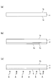
- (A) shows the piezoelectric material substrate 1
- (b) shows the state in which the second bonding layer 2 is provided on the piezoelectric material substrate 1
- (c) shows the second bonding layer 2.
- the state where the surface 2a is activated by the neutralizing beam A to be the activation surface 5 is shown.
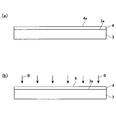
- (A) shows a state in which the first bonding layer 4 is provided on the support substrate 3, and (b) shows a surface 4a of the first bonding layer 4 activated by the neutralizing beam B to be an activation surface.
- a state of 6 is shown.
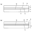
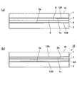
- (A) shows a state where the first bonding layer 4 and the second bonding layer 2 are in contact with each other, and (b) shows a state where the first bonding layer 4A and the second bonding layer 2A are bonded to each other.
- the state which produced the joined body 8 is shown.
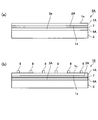
- (A) shows a state in which the piezoelectric material substrate 1A is thinned by processing, and (b) shows a state in which the electrodes 9 are provided on the piezoelectric material substrate 1A.
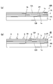
- (A) shows a state where the first bonding layer 4 and the second bonding layer 2 are in contact with each other, and (b) shows a state where the first bonding layer 4A and the second bonding layer 2A are bonded to each other.
- the state which produced the joined body 18 is shown.
- (A) shows a state in which the piezoelectric material substrate 1A is thinned by processing, and (b) shows a state in which the electrodes 9 are provided on the piezoelectric material substrate 1A.
- the piezoelectric material substrate 1 has a pair of main surfaces 1a and 1b.
- the first bonding layer 2 is formed on the main surface 1 a of the piezoelectric material substrate 1.
- the surface 2a of the first bonding layer 2 is irradiated with a neutralizing beam as indicated by an arrow A to activate the surface 2a of the bonding layer 2 to form an activation surface 5.
- the second bonding layer 4 is formed on the main surface 3 a of the supporting substrate 3. Then, as shown in FIG. 2B, the surface 4a of the bonding layer 4 is irradiated with a neutralizing beam as indicated by an arrow B, and the surface 4a of the bonding layer 4 is activated to form an activation surface 6.
- the activation surface 6 of the first bonding layer 4 and the activation surface 5 of the second bonding layer 2 are directly contacted with each other and pressure is applied to the activation surface 6 of FIG. ),
- the bonded body 8 is obtained.
- the bonding interface between the activation surface 6 of the first bonding layer 4 and the activation surface 5 of the second bonding layer 2 is controlled.
- Amorphous layer 7 can be generated along with it.
- the amorphous layer 7 is formed along the interface between the first bonding layer 4A and the second bonding layer 2A.
- the surface 1b of the piezoelectric material substrate 1 of the bonded body 8 is further polished to reduce the thickness of the piezoelectric material substrate 1A as shown in FIG. obtain.
- 1c is a polishing surface.
- the acoustic wave element 10 is manufactured by forming a predetermined electrode 9 on the polished surface 1c of the piezoelectric material substrate 1A.
- the intermediate layer 12A is provided between the piezoelectric material substrate 1 and the second bonding layer 2, and the intermediate layer 12B is provided between the support substrate 3 and the first bonding layer 4. It is provided.
- the intermediate layer 12A and the second bonding layer 2 are sequentially formed on the main surface 1a of the piezoelectric material substrate 1. Then, the surface of the bonding layer 2 is irradiated with a neutralizing beam to activate the surface of the bonding layer 2A to form the activation surface 5.
- the intermediate layer 12B and the first bonding layer 4 are sequentially formed on the main surface 3a of the support substrate 3. Next, each surface of the bonding layers 2 and 4 is irradiated with a neutralizing beam to activate each surface of each bonding layer to form activation surfaces 6 and 5.
- the activation surface 6 of the first bonding layer 4 and the activation surface 5 of the second bonding layer 2 are brought into direct contact with each other, and pressure is applied to the activation surface 6 of FIG. ),
- the joined body 18 is obtained.
- the bonding interface between the activation surface 6 of the first bonding layer 4 and the activation surface 5 of the second bonding layer 2 is controlled.
- Amorphous layer 7 can be generated along with it.
- the amorphous layer 7 is formed along the interface between the first bonding layer 4A and the second bonding layer 2A.
- the surface 1b of the piezoelectric material substrate 1 of the bonded body 18 is further polished to reduce the thickness of the piezoelectric material substrate 1A as shown in FIG. obtain.
- 1c is a polishing surface.
- the acoustic wave element 20 is manufactured by forming a predetermined electrode 9 on the polished surface 1c of the piezoelectric material substrate 1A.
- the supporting substrate may be made of single crystal or polycrystal.
- the material of the supporting substrate is preferably selected from the group consisting of silicon, sialon, sapphire, cordierite, mullite and alumina.
- the alumina is preferably translucent alumina.
- the relative density of the supporting substrate is preferably 99.5% or more, and may be 100%. Relative density is measured by the Archimedes method.
- the method for manufacturing the supporting substrate is not particularly limited, but a sintered body is preferable.
- the silicon may be single crystal silicon, polycrystalline silicon, or high resistance silicon.
- Sialon is a ceramic obtained by sintering a mixture of silicon nitride and alumina, and has the following composition. Si 6-z Al z O z N 8-z That is, sialon has a composition in which alumina is mixed in silicon nitride, and z represents the mixing ratio of alumina. More preferably, z is 0.5 or more. Further, z is more preferably 4.0 or less.
- Sapphire is a single crystal having a composition of Al 2 O 3
- alumina is a polycrystal having a composition of Al 2 O 3
- Cordierite is a ceramic having a composition of 2MgO ⁇ 2Al2O3 ⁇ 5SiO2.
- Mullite is a ceramic having a composition in the range of 3Al2O3 ⁇ 2SiO2 to 2Al2O3 ⁇ SiO2.
- the material of the piezoelectric material substrate is not limited as long as it has necessary piezoelectricity, but a single crystal having a composition of LiAO 3 is preferable.
- A is one or more elements selected from the group consisting of niobium and tantalum. Therefore, LiAO 3 may be lithium niobate, lithium tantalate, or a lithium niobate-lithium tantalate solid solution.
- the first bonding layer is provided on the supporting substrate, and the second bonding layer is provided on the piezoelectric material substrate.
- the first bonding layer has a composition of Si (1-x) O x (0.008 ⁇ x ⁇ 0.408).
- the second bonding layer layer has a composition of Si (1-y) O y (0.008 ⁇ y ⁇ 0.408).
- x and y are set to 0.008 or more, preferably 0.010 or more, more preferably 0.020 or more, and particularly preferably 0.024 or more. If x and y are larger than 0.408, the bonding strength is lowered and the piezoelectric material substrate is easily peeled off. Therefore, x and y are 0.408 or less, but 0.225 or less is more preferable. preferable.
- each bonding layer is preferably 4.8 ⁇ 10 3 ⁇ ⁇ cm or more, more preferably 5.8 ⁇ 10 3 ⁇ ⁇ cm or more, and 6.2 ⁇ 10 3 ⁇ ⁇ cm. The above is particularly preferable.
- the electrical resistivity of the bonding layer is generally 1.0 ⁇ 10 8 ⁇ ⁇ cm or less.
- each bonding layer is not particularly limited, but is preferably 0.01 to 10 ⁇ m, more preferably 0.01 to 0.5 ⁇ m from the viewpoint of manufacturing cost.
- the method for forming each bonding layer is not limited, but examples thereof include a sputtering method, a chemical vapor deposition method (CVD), and vapor deposition.
- CVD chemical vapor deposition method
- each bonding layer The specific manufacturing conditions of each bonding layer are appropriately selected because they depend on the chamber specifications, but in the preferred example, the total pressure is 0.28 to 0.34 Pa and the oxygen partial pressure is 1.2 ⁇ 10 ⁇ 3 to 5.7.
- the film formation temperature is room temperature, and the film formation temperature is ⁇ 10 ⁇ 2 Pa.
- B-doped Si can be exemplified as the Si target.
- the amount of B (boron) as an impurity is 5 ⁇ 10 18 atoms / cm 3 to 5 ⁇ 10 19 atoms at the interface with the first bonding layer and the interface with the second bonding layer and the rest. It is controlled to be about / cm 3 . As a result, the insulating property of the bonding layer can be more reliably ensured.
- the activation surface of the first bonding layer and the activation surface of the second bonding layer are directly bonded.
- the arithmetic average roughness Ra of each activated surface of each bonding layer is preferably 1 nm or less, and more preferably 0.3 nm or less. This further improves the bonding strength.
- the bonded body of the present invention includes an amorphous layer formed between the first bonding layer and the second bonding layer, and the oxygen ratio in the amorphous layer is the oxygen ratio in the first bonding layer. And higher than the oxygen ratio in the second bonding layer. That is, although an amorphous layer is formed along the activated surface of the support substrate, the oxygen ratio in the first bonding layer and the second bonding layer in the second bonding layer are increased by the progress of oxygen diffusion in this amorphous layer. It was found that the oxygen ratio in the amorphous layer formed between them may be higher than the oxygen ratio.
- the bonding strength of the piezoelectric material substrate to the supporting substrate increases, and even when the piezoelectric material substrate is thinned by processing, the piezoelectric material substrate is peeled off. I found that is hard to occur.
- the difference between the oxygen ratio in the amorphous layer and the oxygen ratio in the first bonding layer and the difference between the oxygen ratio in the amorphous layer and the oxygen ratio in the second bonding layer are both 0. It is 5 atomic% or more. This difference is more preferably 1.0 atomic% or more. There is no particular upper limit to the difference between the oxygen ratio in the amorphous layer and the oxygen ratio in the first bonding layer and the difference between the oxygen ratio in the amorphous layer and the oxygen ratio in the second bonding layer, Is preferably 5.0 at% or less, more preferably 4.5 at% or less.
- the ratio of argon in the amorphous layer is higher than the ratio of argon in the first bonding layer and the ratio of argon in the second bonding layer.
- the difference between the argon ratio in the amorphous layer and the argon ratio in the first bonding layer and the difference between the argon ratio in the amorphous layer and the argon ratio in the second bonding layer are 1.0 atomic%. It is preferably not less than 1.5%, more preferably not less than 1.5 atomic%. Although there is no particular upper limit for the difference between the argon ratio in the amorphous layer and the argon ratio in the first bonding layer and the difference between the argon ratio in the amorphous layer and the argon ratio in the second bonding layer, there is no practical limit. Is preferably 5.0 at% or less, more preferably 4.5 at% or less.
- the composition of the amorphous layer is based on silicon (Si), oxygen (O) and argon (Ar).
- Si silicon
- oxygen oxygen
- Ar argon
- “to be a main component” means that the total atomic ratio of these atoms is 95 atomic% or more, when the total atomic ratio is 100 atomic%. More preferably, Particularly preferably, the composition of the amorphous layer is Si (1-t) O t (0.013 ⁇ t ⁇ 0.408), and the oxygen ratio is higher than that of the first bonding layer and the second bonding layer. It is also high and contains argon.
- the material of the intermediate layer between the supporting substrate and the first bonding layer and the intermediate layer between the piezoelectric material substrate and the second bonding layer are not particularly limited as long as they are materials that bond to both, but SiO 2 , Ta 2 O 5 , TiO 2 , ZrO 2 , HfO 2 , Nb 2 O 3 , Bi 2 O 3 , Al 2 O 3 , MgO, AlN, and Si 3 N 4 are preferable.
- the intermediate layer between the supporting substrate and the first bonding layer Each material of the intermediate layer between the piezoelectric material substrate and the second bonding layer is preferably a high acoustic velocity material.
- the sound velocity of such a high sonic material is preferably 6000 m / s or more, more preferably 10,000 m / s or more.
- There is no particular upper limit to the sound velocity of each material of each intermediate layer but in practice it is difficult to exceed 30,000 m / s, so it is often 30,000 m / s or less, and further 25,000 m / s or less.
- Examples of such a high sonic velocity material include AlN and Si 3 N 4 .
- the sound velocity of the material is calculated from the density (JIS C2141), Young's modulus (JIS R1602), and Poisson's ratio (JIS R1602) measured by the JIS method.
- the intermediate layer between the supporting substrate and the first bonding layer and the intermediate layer between the piezoelectric material substrate and the second bonding layer are made of high thermal conductive materials.
- the thermal conductivity of such a high thermal conductive material is preferably 100 W / (mK) or more, more preferably 900 W / (mK) or more, and 1000 W / (mK). Particularly preferred.
- thermal conductivity of each material of each intermediate layer there is no particular upper limit to the thermal conductivity of each material of each intermediate layer, but in reality it is difficult to exceed 5000 W / (mK), so 5000 W / (mK) or less, or even 3000 W / (mK). K) or less.
- Examples of such a high heat conductive material include AlN and Si 3 N 4 .
- the thermal conductivity of the material shall be measured according to JIS R1611.
- the application of the bonded body of the present invention is not particularly limited, and can be suitably applied to, for example, an acoustic wave element or an optical element.
- Known surface acoustic wave devices include surface acoustic wave devices, Lamb wave devices, and thin film resonators (FBARs).
- FBARs thin film resonators
- an IDT (Interdigital Transducer) electrode also called a comb-shaped electrode or a comb-shaped electrode
- the IDT electrode on the input side for exciting surface acoustic waves and an output side for receiving surface acoustic waves are provided on the surface of a piezoelectric material substrate.
- the IDT electrode Interdigital Transducer
- the piezoelectric material substrate may have a metal film on the bottom surface.
- the metal film plays a role of increasing the electromechanical coupling coefficient in the vicinity of the back surface of the piezoelectric material substrate when a Lamb wave element is manufactured as an acoustic wave device.
- the Lamb wave element has a structure in which the comb-teeth electrode is formed on the surface of the piezoelectric material substrate and the metal film of the piezoelectric material substrate is exposed by the cavity provided in the supporting substrate.
- Examples of the material of such a metal film include aluminum, aluminum alloy, copper, gold and the like.
- the bottom surface of the piezoelectric material substrate may have a metal film and an insulating film.
- the metal film plays a role of an electrode when a thin film resonator is manufactured as an acoustic wave device.
- the thin film resonator has a structure in which electrodes are formed on the front and back surfaces of the piezoelectric material substrate and the insulating film serves as a cavity to expose the metal film of the piezoelectric material substrate.
- Examples of the material of such a metal film include molybdenum, ruthenium, tungsten, chromium, aluminum and the like.
- examples of the material of the insulating film include silicon dioxide, phosphorus silica glass, boron phosphorus silica glass, and the like.
- examples of the optical element include an optical switching element, a wavelength conversion element, and an optical modulation element.
- examples of the optical element include an optical switching element, a wavelength conversion element, and an optical modulation element.
- a periodic domain inversion structure can be formed in the piezoelectric material substrate.
- the object of the present invention is an acoustic wave device and the material of the piezoelectric material substrate is lithium tantalate, 36 to 47 from the Y axis to the Z axis around the X axis which is the propagation direction of the surface acoustic wave. It is preferable to use the direction rotated by (for example, 42 °) because propagation loss is small.
- the piezoelectric material substrate is made of lithium niobate
- the piezoelectric material substrate should be rotated by 60 to 68 ° (eg, 64 °) from the Y axis to the Z axis about the X axis which is the propagation direction of the surface acoustic wave. It is preferable to use it because the propagation loss is small.
- the size of the piezoelectric material substrate is not particularly limited, but is, for example, 50 to 150 mm in diameter and 0.2 to 60 ⁇ m in thickness.
- each surface of each bonding layer is flattened to obtain a flat surface.
- a method for flattening each surface there are lap polishing, chemical mechanical polishing (CMP), and the like.
- the flat surface preferably has Ra ⁇ 1 nm, and more preferably 0.3 nm or less.
- each surface of each bonding layer is washed in order to remove the residue of the polishing agent and the work-affected layer.
- Methods for cleaning the surface include wet cleaning, dry cleaning, and scrub cleaning. Scrub cleaning is preferable in order to obtain a clean surface easily and efficiently. In this case, it is particularly preferable to use Sunwash LH540 as a cleaning liquid and then to wash with a scrubbing machine using a mixed solution of acetone and IPA.
- each surface of each bonding layer is irradiated with a neutralizing beam to activate each surface.
- the surface activation is performed by the neutralizing beam
- the atomic species forming the beam are preferably an inert gas (argon, nitrogen, etc.).
- the voltage upon activation by beam irradiation is preferably 0.5 to 2.0 kV, and the current is preferably 50 to 200 mA.
- the temperature at this time is room temperature, but specifically, it is preferably 40 ° C. or lower, more preferably 30 ° C. or lower. Moreover, the temperature at the time of joining is particularly preferably 20 ° C. or higher and 25 ° C. or lower. The pressure at the time of joining is preferably 100 to 20000N.
- Examples 1, 2, 3, 3-2, Comparative Examples 1, 2 According to the method described with reference to FIGS. 1 and 2, the bonded bodies 8 and 8A of each example shown in Tables 1 and 2 were produced. Specifically, a lithium tantalate substrate (LT substrate) having an OF portion, a diameter of 4 inches, and a thickness of 250 ⁇ m was used as the piezoelectric material substrate 1. As the LT substrate, a 46 ° Y-cut X-propagation LT substrate in which the propagation direction of the surface acoustic wave (SAW) was X and the cutting angle was a rotating Y-cut plate was used.
- SAW surface acoustic wave
- the surface 1a of the piezoelectric material substrate 1 was mirror-polished so that the arithmetic average roughness Ra was 0.3 nm.
- Ra is measured by an atomic force microscope (AFM) in a visual field of 10 ⁇ m ⁇ 10 ⁇ m.
- the bonding layer 2 was formed on the surface 1a of the piezoelectric material substrate 1 by the DC sputtering method. Boron-doped Si was used as the target. Also, oxygen gas was introduced as an oxygen source. At this time, by changing the oxygen gas introduction amount, the total pressure of the atmosphere in the chamber and the oxygen partial pressure were changed, thereby changing the oxygen ratio of the bonding layer 2.
- the thickness of the bonding layer 2 was 100 to 200 nm.
- the arithmetic average roughness Ra of the surface 2a of the bonding layer 2 was 0.2 to 0.6 nm.
- the bonding layer 2 was subjected to chemical mechanical polishing (CMP) to have a film thickness of 80 to 190 nm and Ra of 0.08 to 0.4 nm.
- CMP chemical mechanical polishing
- a supporting substrate 3 made of silicon having an orientation flat (OF) portion, a diameter of 4 inches, and a thickness of 500 ⁇ m was prepared.
- the surface of the support substrate 3 is finished by chemical mechanical polishing (CMP), and each arithmetic average roughness Ra is 0.2 nm.
- the bonding layer 4 was formed on the surface 3a of the support substrate 3 by the DC sputtering method. Boron-doped Si was used as the target. Also, oxygen gas was introduced as an oxygen source. At this time, by changing the oxygen gas introduction amount, the total pressure of the atmosphere in the chamber and the oxygen partial pressure were changed, thereby changing the oxygen ratio of the bonding layer 4.
- the thickness of the bonding layer 4 was 100 to 200 nm.
- the arithmetic average roughness Ra of the surface 4a of the bonding layer 4 was 0.2 to 0.6 nm.
- the bonding layer 2 was subjected to chemical mechanical polishing (CMP) to have a film thickness of 80 to 190 nm and Ra of 0.08 to 0.4 nm.
- CMP chemical mechanical polishing
- each surface was irradiated with a high-speed atomic beam (accelerating voltage 1 kV, Ar flow rate 27 sccm) for 120 seconds.
- the beam irradiation surface (activation surface) 5 of the bonding layer 2 and the activation surface 6 of the bonding layer 4 were brought into contact with each other, and then pressure was applied for 2 minutes at 10,000 N to bond them (see FIG. 3B).
- the obtained bonded body 8 of each example was heated at 100 ° C. for 20 hours.
- the surface of the piezoelectric material substrate 1 was ground and polished so as to have a thickness of 1 ⁇ m from the initial 250 ⁇ m (see FIG. 4A).
- FIB Frecused Ion Beam
- Elemental analysis by EDS was performed using the following apparatus to measure the ratio of oxygen atoms and argon atoms in the bonding layer and the amorphous layer.
- measuring device Perform elemental analysis using an elemental analyzer (JEOL JEM-ARM200F).
- Measurement condition The sample thinned by the FIB (Focused Ion Beam) method is observed at an acceleration voltage of 200 kV.
- Example 4 Comparative Example 4
- the material of the supporting substrate was changed to sapphire, and the FAB irradiation amount was also changed.
- Others were made in the same manner as in Example 1 to produce the bonded bodies 8 and 8A, and the oxygen ratio, argon ratio, silicon ratio and bonding strength of each part were measured. The results are shown in Table 3.
- Example 4 the oxygen ratio in the amorphous layer was slightly lower than the oxygen ratio in the first bonding layer and was the same as the oxygen ratio in the second bonding layer, but the bonding strength was low.
- the oxygen ratio and the argon ratio in the amorphous layer are higher than the oxygen ratio and the argon ratio in the first bonding layer and the second bonding layer, but the bonding strength is remarkably improved and the piezoelectric property is high. No peeling occurred even when polishing the material substrate.
- Example 5 Comparative Example 5
- the material of the supporting substrate was changed to cordierite, and the FAB irradiation amount was also changed.
- Others were made in the same manner as in Example 1 to produce the bonded bodies 8 and 8A, and the oxygen ratio, argon ratio, silicon ratio and bonding strength of each part were measured. The results are shown in Table 4.
- Example 5 the oxygen ratio in the amorphous layer was the same as the oxygen ratio in the first bonding layer and the second bonding layer, but the bonding strength was low.
- the oxygen ratio and the argon ratio in the amorphous layer were higher than the oxygen ratio and the argon ratio in the first bonding layer and the second bonding layer, but the bonding strength was remarkably improved and the piezoelectric property was improved. No peeling occurred even when polishing the material substrate.
- Example 6 Comparative Example 6
- Others were made in the same manner as in Example 1 to produce the bonded bodies 8 and 8A, and the oxygen ratio, argon ratio, silicon ratio and bonding strength of each part were measured. The results are shown in Table 5.
- the oxygen ratio in the amorphous layer was the same as the oxygen ratio in the first bonding layer and was slightly lower than the oxygen ratio in the second bonding layer, but the bonding strength was low.
- the oxygen ratio and the argon ratio in the amorphous layer are higher than the oxygen ratio and the argon ratio in the first bonding layer and the second bonding layer, but the bonding strength is remarkably improved and the piezoelectric property is high. No peeling occurred even when polishing the material substrate.
- Example 7 Comparative Example 7
- the material of the supporting substrate was changed to mullite, and the FAB irradiation amount was also changed.
- Others were made in the same manner as in Example 1 to produce the bonded bodies 8 and 8A, and the oxygen ratio, argon ratio, silicon ratio and bonding strength of each part were measured. The results are shown in Table 6.
- Example 7 the oxygen ratio in the amorphous layer was the same as the oxygen ratio in the first bonding layer and the second bonding layer, but the bonding strength was low.
- the oxygen ratio and the argon ratio in the amorphous layer were higher than the oxygen ratio and the argon ratio in the first bonding layer and the second bonding layer, but the bonding strength was significantly improved and the piezoelectric property No peeling occurred even when polishing the material substrate.
- Example 8 Comparative Example 8
- the material of the supporting substrate was changed to translucent alumina, and the FAB irradiation amount was also changed.
- Others were made in the same manner as in Example 1 to produce the bonded bodies 8 and 8A, and the oxygen ratio, argon ratio, silicon ratio and bonding strength of each part were measured. The results are shown in Table 7.
- Example 8 the oxygen ratio in the amorphous layer was slightly lower than the oxygen ratios in the first bonding layer and the second bonding layer, but the bonding strength was low.
- the oxygen ratio and the argon ratio in the amorphous layer are higher than the oxygen ratio and the argon ratio in the first bonding layer and the second bonding layer, but the bonding strength is remarkably improved and the piezoelectric property is high. No peeling occurred even when polishing the material substrate.
Landscapes
- Physics & Mathematics (AREA)
- Acoustics & Sound (AREA)
- Engineering & Computer Science (AREA)
- Chemical & Material Sciences (AREA)
- Materials Engineering (AREA)
- Manufacturing & Machinery (AREA)
- Surface Acoustic Wave Elements And Circuit Networks Thereof (AREA)
Abstract
Priority Applications (5)
| Application Number | Priority Date | Filing Date | Title |
|---|---|---|---|
| JP2020552559A JP7069338B2 (ja) | 2018-10-17 | 2019-08-23 | 接合体および弾性波素子 |
| CN201980067483.8A CN112840563B (zh) | 2018-10-17 | 2019-08-23 | 接合体及弹性波元件 |
| KR1020217010298A KR102639041B1 (ko) | 2018-10-17 | 2019-08-23 | 접합체 및 탄성파 소자 |
| DE112019004570.9T DE112019004570B4 (de) | 2018-10-17 | 2019-08-23 | Verbundener Körper und Akustikwellenelement |
| US17/231,429 US11888462B2 (en) | 2018-10-17 | 2021-04-15 | Bonded body and acoustic wave element |
Applications Claiming Priority (2)
| Application Number | Priority Date | Filing Date | Title |
|---|---|---|---|
| JP2018-195663 | 2018-10-17 | ||
| JP2018195663 | 2018-10-17 |
Related Child Applications (1)
| Application Number | Title | Priority Date | Filing Date |
|---|---|---|---|
| US17/231,429 Continuation US11888462B2 (en) | 2018-10-17 | 2021-04-15 | Bonded body and acoustic wave element |
Publications (1)
| Publication Number | Publication Date |
|---|---|
| WO2020079959A1 true WO2020079959A1 (fr) | 2020-04-23 |
Family
ID=70284560
Family Applications (1)
| Application Number | Title | Priority Date | Filing Date |
|---|---|---|---|
| PCT/JP2019/033130 Ceased WO2020079959A1 (fr) | 2018-10-17 | 2019-08-23 | Corps lié et élément à ondes acoustiques |
Country Status (7)
| Country | Link |
|---|---|
| US (1) | US11888462B2 (fr) |
| JP (1) | JP7069338B2 (fr) |
| KR (1) | KR102639041B1 (fr) |
| CN (1) | CN112840563B (fr) |
| DE (1) | DE112019004570B4 (fr) |
| TW (1) | TWI811454B (fr) |
| WO (1) | WO2020079959A1 (fr) |
Cited By (6)
| Publication number | Priority date | Publication date | Assignee | Title |
|---|---|---|---|---|
| WO2022250016A1 (fr) * | 2021-05-27 | 2022-12-01 | 株式会社村田製作所 | Dispositif à ondes élastiques |
| JPWO2023182246A1 (fr) * | 2022-03-23 | 2023-09-28 | ||
| EP4131777A4 (fr) * | 2021-03-25 | 2023-11-22 | NGK Insulators, Ltd. | Corps lié et son procédé de production |
| JP7510558B1 (ja) | 2023-11-14 | 2024-07-03 | 日本碍子株式会社 | 複合基板および複合基板の製造方法 |
| WO2025105352A1 (fr) * | 2023-11-14 | 2025-05-22 | 日本碍子株式会社 | Substrat composite, et procédé de fabrication de celui-ci |
| JP2025101723A (ja) * | 2023-12-25 | 2025-07-07 | 日本碍子株式会社 | 複合基板 |
Families Citing this family (2)
| Publication number | Priority date | Publication date | Assignee | Title |
|---|---|---|---|---|
| JP2025518169A (ja) * | 2022-05-30 | 2025-06-12 | スカイワークス ソリューションズ,インコーポレイテッド | 高速高次モードを有する弾性表面波デバイス |
| CN121057718A (zh) * | 2023-05-09 | 2025-12-02 | 日本碍子株式会社 | 接合体 |
Citations (3)
| Publication number | Priority date | Publication date | Assignee | Title |
|---|---|---|---|---|
| JP2004343359A (ja) * | 2003-05-14 | 2004-12-02 | Fujitsu Media Device Kk | 弾性表面波素子の製造方法 |
| WO2017134980A1 (fr) * | 2016-02-02 | 2017-08-10 | 信越化学工業株式会社 | Substrat composite et procédé de production de substrat composite |
| WO2018180827A1 (fr) * | 2017-03-31 | 2018-10-04 | 日本碍子株式会社 | Corps lié et élément à ondes acoustiques |
Family Cites Families (10)
| Publication number | Priority date | Publication date | Assignee | Title |
|---|---|---|---|---|
| JP2002201459A (ja) * | 2000-12-28 | 2002-07-19 | Nichias Corp | ジョイントシート |
| US7105980B2 (en) | 2002-07-03 | 2006-09-12 | Sawtek, Inc. | Saw filter device and method employing normal temperature bonding for producing desirable filter production and performance characteristics |
| CN100480736C (zh) * | 2004-09-16 | 2009-04-22 | 尼康股份有限公司 | MgF2光学薄膜和具备该薄膜的光学组件以及该薄膜的制造方法 |
| CN102624352B (zh) | 2010-10-06 | 2015-12-09 | 日本碍子株式会社 | 复合基板的制造方法以及复合基板 |
| JP2014086400A (ja) | 2012-10-26 | 2014-05-12 | Mitsubishi Heavy Ind Ltd | 高速原子ビーム源およびそれを用いた常温接合装置 |
| KR101450429B1 (ko) * | 2013-01-24 | 2014-10-14 | 주식회사 효성 | 라지토우용 탄소섬유 전구체 섬유 |
| JP6117134B2 (ja) * | 2014-03-13 | 2017-04-19 | 信越化学工業株式会社 | 複合基板の製造方法 |
| KR20190134827A (ko) * | 2016-03-25 | 2019-12-04 | 엔지케이 인슐레이터 엘티디 | 접합체 및 탄성파 소자 |
| WO2018011256A1 (fr) | 2016-07-14 | 2018-01-18 | Sanofi-Aventis Deutschland Gmbh | Dispositif d'administration de médicament à protection d'aiguille et manchon de protection commandés |
| JP6393015B1 (ja) * | 2017-05-02 | 2018-09-19 | 日本碍子株式会社 | 弾性波素子およびその製造方法 |
-
2019
- 2019-08-23 JP JP2020552559A patent/JP7069338B2/ja active Active
- 2019-08-23 WO PCT/JP2019/033130 patent/WO2020079959A1/fr not_active Ceased
- 2019-08-23 KR KR1020217010298A patent/KR102639041B1/ko active Active
- 2019-08-23 DE DE112019004570.9T patent/DE112019004570B4/de active Active
- 2019-08-23 CN CN201980067483.8A patent/CN112840563B/zh active Active
- 2019-09-23 TW TW108134160A patent/TWI811454B/zh active
-
2021
- 2021-04-15 US US17/231,429 patent/US11888462B2/en active Active
Patent Citations (3)
| Publication number | Priority date | Publication date | Assignee | Title |
|---|---|---|---|---|
| JP2004343359A (ja) * | 2003-05-14 | 2004-12-02 | Fujitsu Media Device Kk | 弾性表面波素子の製造方法 |
| WO2017134980A1 (fr) * | 2016-02-02 | 2017-08-10 | 信越化学工業株式会社 | Substrat composite et procédé de production de substrat composite |
| WO2018180827A1 (fr) * | 2017-03-31 | 2018-10-04 | 日本碍子株式会社 | Corps lié et élément à ondes acoustiques |
Cited By (9)
| Publication number | Priority date | Publication date | Assignee | Title |
|---|---|---|---|---|
| EP4131777A4 (fr) * | 2021-03-25 | 2023-11-22 | NGK Insulators, Ltd. | Corps lié et son procédé de production |
| WO2022250016A1 (fr) * | 2021-05-27 | 2022-12-01 | 株式会社村田製作所 | Dispositif à ondes élastiques |
| JPWO2023182246A1 (fr) * | 2022-03-23 | 2023-09-28 | ||
| WO2023182246A1 (fr) * | 2022-03-23 | 2023-09-28 | 京セラ株式会社 | Substrat lié |
| JP7510558B1 (ja) | 2023-11-14 | 2024-07-03 | 日本碍子株式会社 | 複合基板および複合基板の製造方法 |
| WO2025105352A1 (fr) * | 2023-11-14 | 2025-05-22 | 日本碍子株式会社 | Substrat composite, et procédé de fabrication de celui-ci |
| JP2025080665A (ja) * | 2023-11-14 | 2025-05-26 | 日本碍子株式会社 | 複合基板および複合基板の製造方法 |
| JP2025101723A (ja) * | 2023-12-25 | 2025-07-07 | 日本碍子株式会社 | 複合基板 |
| JP7791281B2 (ja) | 2023-12-25 | 2025-12-23 | 日本碍子株式会社 | 複合基板 |
Also Published As
| Publication number | Publication date |
|---|---|
| TW202023810A (zh) | 2020-07-01 |
| CN112840563A (zh) | 2021-05-25 |
| US11888462B2 (en) | 2024-01-30 |
| TWI811454B (zh) | 2023-08-11 |
| CN112840563B (zh) | 2025-02-07 |
| KR20210058873A (ko) | 2021-05-24 |
| KR102639041B1 (ko) | 2024-02-20 |
| JPWO2020079959A1 (ja) | 2021-09-24 |
| DE112019004570T5 (de) | 2021-06-02 |
| DE112019004570B4 (de) | 2022-10-13 |
| JP7069338B2 (ja) | 2022-05-17 |
| US20210234530A1 (en) | 2021-07-29 |
Similar Documents
| Publication | Publication Date | Title |
|---|---|---|
| JP7133031B2 (ja) | 接合体および弾性波素子 | |
| JP7069338B2 (ja) | 接合体および弾性波素子 | |
| JP6375471B1 (ja) | 接合体および弾性波素子 | |
| JP6731539B2 (ja) | 弾性波素子およびその製造方法 | |
| TWI737811B (zh) | 接合體 | |
| JP6708773B2 (ja) | 接合体および弾性波素子 | |
| KR20210006995A (ko) | 접합체 및 탄성파 소자 | |
| JPWO2019244471A1 (ja) | 接合体および弾性波素子 | |
| JPWO2019188350A1 (ja) | 接合体および弾性波素子 | |
| JP6612002B1 (ja) | 接合体および弾性波素子 | |
| JPWO2021002046A1 (ja) | 接合体および弾性波素子 | |
| JP6621574B1 (ja) | 接合体および弾性波素子 | |
| JPWO2021002047A1 (ja) | 接合体および弾性波素子 |
Legal Events
| Date | Code | Title | Description |
|---|---|---|---|
| 121 | Ep: the epo has been informed by wipo that ep was designated in this application |
Ref document number: 19873628 Country of ref document: EP Kind code of ref document: A1 |
|
| ENP | Entry into the national phase |
Ref document number: 2020552559 Country of ref document: JP Kind code of ref document: A |
|
| ENP | Entry into the national phase |
Ref document number: 20217010298 Country of ref document: KR Kind code of ref document: A |
|
| 122 | Ep: pct application non-entry in european phase |
Ref document number: 19873628 Country of ref document: EP Kind code of ref document: A1 |
|
| WWG | Wipo information: grant in national office |
Ref document number: 201980067483.8 Country of ref document: CN |