WO2025105352A1 - Substrat composite, et procédé de fabrication de celui-ci - Google Patents
Substrat composite, et procédé de fabrication de celui-ci Download PDFInfo
- Publication number
- WO2025105352A1 WO2025105352A1 PCT/JP2024/040057 JP2024040057W WO2025105352A1 WO 2025105352 A1 WO2025105352 A1 WO 2025105352A1 JP 2024040057 W JP2024040057 W JP 2024040057W WO 2025105352 A1 WO2025105352 A1 WO 2025105352A1
- Authority
- WO
- WIPO (PCT)
- Prior art keywords
- layer
- refractive index
- multilayer film
- oxide
- wavelength conversion
- Prior art date
- Legal status (The legal status is an assumption and is not a legal conclusion. Google has not performed a legal analysis and makes no representation as to the accuracy of the status listed.)
- Pending
Links
Images



Classifications
-
- B—PERFORMING OPERATIONS; TRANSPORTING
- B23—MACHINE TOOLS; METAL-WORKING NOT OTHERWISE PROVIDED FOR
- B23K—SOLDERING OR UNSOLDERING; WELDING; CLADDING OR PLATING BY SOLDERING OR WELDING; CUTTING BY APPLYING HEAT LOCALLY, e.g. FLAME CUTTING; WORKING BY LASER BEAM
- B23K20/00—Non-electric welding by applying impact or other pressure, with or without the application of heat, e.g. cladding or plating
-
- G—PHYSICS
- G02—OPTICS
- G02B—OPTICAL ELEMENTS, SYSTEMS OR APPARATUS
- G02B1/00—Optical elements characterised by the material of which they are made; Optical coatings for optical elements
- G02B1/10—Optical coatings produced by application to, or surface treatment of, optical elements
- G02B1/11—Anti-reflection coatings
- G02B1/113—Anti-reflection coatings using inorganic layer materials only
- G02B1/115—Multilayers
-
- G—PHYSICS
- G02—OPTICS
- G02B—OPTICAL ELEMENTS, SYSTEMS OR APPARATUS
- G02B5/00—Optical elements other than lenses
- G02B5/20—Filters
-
- G—PHYSICS
- G02—OPTICS
- G02B—OPTICAL ELEMENTS, SYSTEMS OR APPARATUS
- G02B5/00—Optical elements other than lenses
- G02B5/20—Filters
- G02B5/22—Absorbing filters
-
- G—PHYSICS
- G02—OPTICS
- G02B—OPTICAL ELEMENTS, SYSTEMS OR APPARATUS
- G02B5/00—Optical elements other than lenses
- G02B5/20—Filters
- G02B5/26—Reflecting filters
-
- G—PHYSICS
- G02—OPTICS
- G02B—OPTICAL ELEMENTS, SYSTEMS OR APPARATUS
- G02B5/00—Optical elements other than lenses
- G02B5/20—Filters
- G02B5/28—Interference filters
-
- H—ELECTRICITY
- H01—ELECTRIC ELEMENTS
- H01S—DEVICES USING THE PROCESS OF LIGHT AMPLIFICATION BY STIMULATED EMISSION OF RADIATION [LASER] TO AMPLIFY OR GENERATE LIGHT; DEVICES USING STIMULATED EMISSION OF ELECTROMAGNETIC RADIATION IN WAVE RANGES OTHER THAN OPTICAL
- H01S3/00—Lasers, i.e. devices using stimulated emission of electromagnetic radiation in the infrared, visible or ultraviolet wave range
- H01S3/05—Construction or shape of optical resonators; Accommodation of active medium therein; Shape of active medium
-
- H—ELECTRICITY
- H01—ELECTRIC ELEMENTS
- H01S—DEVICES USING THE PROCESS OF LIGHT AMPLIFICATION BY STIMULATED EMISSION OF RADIATION [LASER] TO AMPLIFY OR GENERATE LIGHT; DEVICES USING STIMULATED EMISSION OF ELECTROMAGNETIC RADIATION IN WAVE RANGES OTHER THAN OPTICAL
- H01S5/00—Semiconductor lasers
- H01S5/02—Structural details or components not essential to laser action
- H01S5/022—Mountings; Housings
- H01S5/0239—Combinations of electrical or optical elements
-
- H—ELECTRICITY
- H01—ELECTRIC ELEMENTS
- H01S—DEVICES USING THE PROCESS OF LIGHT AMPLIFICATION BY STIMULATED EMISSION OF RADIATION [LASER] TO AMPLIFY OR GENERATE LIGHT; DEVICES USING STIMULATED EMISSION OF ELECTROMAGNETIC RADIATION IN WAVE RANGES OTHER THAN OPTICAL
- H01S5/00—Semiconductor lasers
- H01S5/10—Construction or shape of the optical resonator, e.g. extended or external cavity, coupled cavities, bent-guide, varying width, thickness or composition of the active region
- H01S5/18—Surface-emitting [SE] lasers, e.g. having both horizontal and vertical cavities
- H01S5/183—Surface-emitting [SE] lasers, e.g. having both horizontal and vertical cavities having only vertical cavities, e.g. vertical cavity surface-emitting lasers [VCSEL]
Definitions
- the present invention relates to a composite substrate and a method for manufacturing the composite substrate.
- Solid-state lasers capable of outputting short pulses of light are widely used. Lasers with extremely high optical output with shorter pulse widths are expected to be applied in various fields such as sensing, precision machining, and medicine.
- a laser structure has been proposed that combines a semiconductor laser, a solid-state laser gain medium layer that can function as a wavelength conversion layer, and a saturable absorber.
- the light reflection characteristics at the wavelength conversion layer interface can significantly affect the performance of the laser.
- the present invention has been made in consideration of the above, and its main objective is to provide a composite substrate with excellent reflection characteristics at the wavelength conversion layer interface.
- a composite substrate includes a wavelength conversion layer that converts incident light into light with a different wavelength, and a multilayer film disposed adjacent to the wavelength conversion layer, the multilayer film including a plurality of refractive index layers, a region having an abundance of inert gas atoms of 0.5 atomic % or more is formed at an end of the wavelength conversion layer on the side where the multilayer film is disposed, and an abundance of inert gas atoms in a first refractive index layer located closest to the wavelength conversion layer of the multilayer film is less than 0.5 atomic %.
- the refractive index of each of the plurality of refractive index layers included in the multilayer film may be 1.3 to 2.4, and the multilayer film may include one or more refractive index layers having a refractive index of 2.1 or more. 3.
- the wavelength conversion layer and the first refractive index layer may be bonded to each other. 4.
- the inert gas atoms may be argon or xenon. 5.
- the difference in refractive index between the layer having the highest refractive index and the layer having the lowest refractive index may be 0.5 or more.
- the wavelength conversion layer may be selected from a doped yttrium aluminum garnet crystal, a doped yttrium vanadate crystal, and a doped yttrium lithium fluoride crystal. 7.
- the material constituting each refractive index layer included in the multilayer film may be selected from silicon oxide, tantalum oxide, titanium oxide, aluminum oxide, yttrium oxide, zirconium oxide, hafnium oxide, lanthanum oxide, cerium oxide, tungsten oxide, zinc oxide, niobium oxide, and magnesium oxide.
- the material constituting the first refractive index layer may be selected from tantalum oxide, titanium oxide, aluminum oxide, yttrium oxide, zirconium oxide, hafnium oxide, lanthanum oxide, cerium oxide, tungsten oxide, zinc oxide, niobium oxide and magnesium oxide.
- an end portion in a thickness direction of the wavelength conversion layer may include, in order from the multilayer film side, a third layer, a second layer, and a first layer, and an amount of inert gas atoms in the second layer may be greater than an amount of inert gas atoms in the third layer.
- the third layer may be an amorphous layer.
- the first refractive index layer may have a uniform refractive index in a thickness direction. 12.
- the refractive indexes of two adjacent refractive index layers included in the multilayer film may be different. 13.
- the thickness of each of the refractive index layers included in the multilayer film may be 50 nm or more and 300 nm or less.
- the composite substrate according to any one of 1 to 13 above may include the wavelength conversion layer, the multilayer film, and a surface-emitting laser substrate in this order.
- the composite substrate according to any one of 1 to 14 above may have the wavelength conversion layer, the multilayer film, and a saturable absorbing layer in this order. 16.
- a composite substrate according to another embodiment of the present invention includes a surface-emitting laser substrate, a wavelength conversion layer that converts incident light into light with a different wavelength, and a saturable absorbing layer, in that order, and a multilayer film disposed adjacent to the wavelength conversion layer at least one of between the surface-emitting laser substrate and the wavelength conversion layer and between the saturable absorbing layer and the wavelength conversion layer, the multilayer film includes a plurality of refractive index layers, a region having an abundance of inert gas atoms of 0.5 atomic % or more is formed at an end of the wavelength conversion layer on the side where the multilayer film is disposed, and the abundance of inert gas atoms in a first refractive index layer located closest to the wavelength conversion layer of the multilayer film is less than 0.5 atomic %. 17.
- a laser structure according to an embodiment of the present invention includes a composite substrate according to any one of 1 to 16 above.
- a manufacturing method of a composite substrate according to an embodiment of the present invention is a manufacturing method of a composite substrate according to any one of 1 to 17 above, which includes, in this order, preparing a laminated structure of a plurality of refractive index layers, performing an activation treatment on each of a surface of a wavelength converting material substrate and a surface of the laminated structure, performing a sputtering treatment on the surface of the wavelength converting material substrate to form a deposition layer containing components constituting the wavelength converting material substrate on the surface of the laminated structure, and bonding the laminated structure and the wavelength converting material substrate. 19.
- the sputtering process may be performed for 3 to 10 minutes.
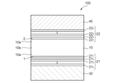
- FIG. 1 is a schematic cross-sectional view showing an outline of a configuration of a composite substrate according to one embodiment of the present invention.
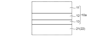
- 4 is a schematic enlarged partial cross-sectional view showing an example of a state of an end portion in a thickness direction of a wavelength conversion layer.
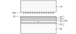
- FIG. 1A to 1C are diagrams illustrating an example of a manufacturing process for a composite substrate according to an embodiment. This is a figure continuing from Figure 3A. This is a figure continuing from Figure 3B. This is a figure continuing from Figure 3C.
- 1 is a graph showing a simulation result of the reflection characteristics of the multilayer film of Example 1.
- 13 is a graph showing a simulation result of the reflection characteristics of the multilayer film of Comparative Example 1.
- 13 is a graph showing a simulation result of the reflection characteristics of the multilayer film of Example 2.
- 13 is a graph showing a simulation result of the reflection characteristics of the multilayer film of Example 3.
- 13 is a graph showing a simulation result of the reflection characteristics of the multilayer film of Example 4.
- 13 is a graph showing a simulation result of the reflection characteristics of the multilayer film of Example 5.
- 13 is a graph showing a simulation result of the reflection characteristics of the multilayer film of Example 6.
- 13 is a graph showing a simulation result of the reflection characteristics of the multilayer film of Example 7.
- FIG. 1 is a schematic cross-sectional view showing a schematic configuration of a composite substrate according to one embodiment of the present invention, in which hatching of some members is omitted in order to make the drawing easier to see.
- the composite substrate 100 has a first main surface 1 and a second main surface 2 facing each other, and includes a wavelength conversion layer 10 that converts incident light into light of a different wavelength, a first multilayer film 21 arranged adjacent to the first main surface 1 of the wavelength conversion layer 10, a second multilayer film 22 arranged adjacent to the second main surface 2 of the wavelength conversion layer 10, a substrate 30 arranged on the first multilayer film 21 side of the wavelength conversion layer 10, and a functional layer 40 arranged on the second multilayer film 22 side of the wavelength conversion layer 10.
- the composite substrate 100 can be applied to, for example, a laser element.
- the substrate 30 is, for example, a substrate constituting a surface-emitting laser (e.g., a vertical-cavity surface-emitting laser (VCSEL) or a vertical-external-cavity vertical surface-emitting laser (VECSEL)).
- a surface-emitting laser e.g., a vertical-cavity surface-emitting laser (VCSEL) or a vertical-external-cavity vertical surface-emitting laser (VECSEL)
- the wavelength conversion layer 10 can convert a first wavelength of laser light incident from the first main surface 1 side to a second wavelength.
- a resonator structure can be provided on the substrate 30.
- the substrate that constitutes the surface-emitting laser may be, for example, a gallium arsenide substrate, an indium phosphide substrate, or a gallium nitride substrate.
- the thickness of the substrate that constitutes the surface-emitting laser is, for example, 100 ⁇ m to 1000 ⁇ m.
- the wavelength conversion layer 10 is made of any suitable wavelength conversion material capable of converting incident light into light of a different wavelength.
- a doped yttrium aluminum garnet (hereinafter referred to as YAG) crystal is typically used.
- the doped YAG crystal include a YAG crystal doped with Yb 3+ (Yb:YAG) and a YAG crystal doped with Nd 3+ (Nd:YAG).
- YVO 4 doped yttrium vanadate
- YLF doped yttrium lithium fluoride
- the doped YVO 4 crystal include a YVO 4 crystal doped with Yb 3+ (Yb:YVO 4 ) and a YVO 4 crystal doped with Nd 3+ (Nd:YVO 4 ).
- doped YLF crystals include Yb 3+ doped YLF crystals (Yb:YLF) and Nd 3+ doped YVO 4 crystals (Nd:YLF).
- Other materials constituting the wavelength conversion layer 10 include, for example, Nd:glass, Yb:FAP, Yb:SFAP, Yb:glass, Yb:KYW, Yb:BCBF, Yb:YCOB, Yb:GdCOB, and Yb:YAB.
- doped YAG crystals, doped YVO 4 crystals, and doped YLF crystals are preferably used as other materials constituting the wavelength conversion layer 10. These may exhibit, for example, the same adhesion to adjacent layers.
- the thickness of the wavelength conversion layer 10 is, for example, 10 ⁇ m to 600 ⁇ m.
- the first multilayer film 21 is a laminate of a plurality of refractive index layers.
- the first multilayer film 21 includes n layers, namely, a first refractive index layer 21 1 , a second refractive index layer 21 2 , a third refractive index layer 21 3 , ..., and an nth refractive index layer 21 n , from the wavelength conversion layer 10 side.
- the refractive index layer located closest to the wavelength conversion layer 10 is the first refractive index layer 21 1
- the refractive index layer located closest to the substrate 30 is the nth refractive index layer 21 n .
- n is, for example, 10 to 50, preferably 15 to 40.
- the thickness of each layer included in the first multilayer film 21 is, for example, 50 nm or more and 300 nm or less.
- the first multilayer film 21 includes a plurality of refractive index layers having different refractive indices, including a high refractive index layer having a relatively high refractive index and a low refractive index layer having a relatively low refractive index.
- the refractive indexes of two adjacent layers included in the first multilayer film 21 are different, one being a high refractive index layer and the other being a low refractive index layer.
- at least a part of the first multilayer film 21 may be configured by alternately stacking a high refractive index layer and a low refractive index layer.
- the refractive index of the second refractive index layer 21 2 may be smaller or larger than the refractive index of the first refractive index layer 21 1 and the refractive index of the third refractive index layer 21 3.
- the refractive index of the first refractive index layer 21 1 and the refractive index of the third refractive index layer 21 3 may be substantially the same or different.
- the first multilayer film 21 is configured to transmit light of a first wavelength emitted from the substrate 30 side. Specifically, the first multilayer film 21 is configured to function as a transmission layer or an anti-reflection layer for light of the first wavelength. The first multilayer film 21 is configured to suppress the emission of light of a second wavelength from the wavelength conversion layer 10 to the substrate 30 side, for example, from the viewpoint of improving light utilization efficiency. Specifically, the first multilayer film 21 is configured to function as a reflection layer for light of the second wavelength. Such a function of the first multilayer film 21 can be realized, for example, by adjusting the number of refractive index layers (n above) constituting the first multilayer film 21, the thickness of each refractive index layer, and the refractive index of each layer.
- the functional layer 40 can function as, for example, a saturable absorbing layer.
- the functional layer (saturable absorbing layer) 40 can be typically made of a material such as a YAG crystal doped with Cr 4+ (Cr:YAG) or a YAG crystal doped with V 3+ (V:YAG).
- the thickness of the functional layer (saturable absorbing layer) 40 is, for example, 10 ⁇ m to 600 ⁇ m.
- the second multilayer film 22 is a laminate of a plurality of refractive index layers.
- the second multilayer film 22 includes, from the wavelength conversion layer 10 side, n layers of a first refractive index layer 22 1 , a second refractive index layer 22 2 , a third refractive index layer 22 3 , ..., and an nth refractive index layer 22 n .
- the layer located closest to the wavelength conversion layer 10 side is the first refractive index layer 22 1
- the layer located closest to the functional layer 40 side is the nth refractive index layer 22 n .
- n is, for example, 10 to 50, preferably 15 to 40.
- the thickness of each of the refractive index layers included in the second multilayer film 22 is, for example, 50 nm or more and 300 nm or less.
- the second multilayer film 22 includes a plurality of refractive index layers having different refractive indices, including a high refractive index layer having a relatively high refractive index and a low refractive index layer having a relatively low refractive index.
- the refractive indexes of two adjacent layers included in the second multilayer film 22 are different, one being a high refractive index layer and the other being a low refractive index layer.
- at least a part of the second multilayer film 22 may be configured by alternately stacking a high refractive index layer and a low refractive index layer.
- the refractive index of the second layer 22 2 may be smaller or larger than the refractive index of the first refractive index layer 22 1 and the refractive index of the third refractive index layer 22 3.
- the refractive index of the first refractive index layer 22 1 and the refractive index of the third refractive index layer 22 3 may be substantially the same or different.
- the second multilayer film 22 is configured to transmit light of the second wavelength emitted from the wavelength conversion layer 10. Specifically, the second multilayer film 22 is configured to function as a transmission layer or an anti-reflection layer for light of the second wavelength. The second multilayer film 22 is configured to suppress the emission of light of the first wavelength from the wavelength conversion layer 10 to the functional layer 40, for example, from the viewpoint of improving light utilization efficiency. Specifically, the second multilayer film 22 is configured to function as a reflection layer for light of the first wavelength. Such a function of the second multilayer film 22 can be realized, for example, by adjusting the number of refractive index layers (n above) constituting the second multilayer film 22, the thickness of each refractive index layer, and the refractive index of each refractive index layer.
- each of the first multilayer film 21 and the second multilayer film 22 is a laminate of multiple refractive index layers, and may include a high refractive index layer and a low refractive index layer with different refractive indexes.
- the refractive index of each refractive index layer included in the multilayer film is, for example, 1.3 to 2.4, preferably 1.4 to 2.4, and more preferably 1.45 to 2.35.
- the refractive index may be a value measured by a spectroscopic ellipsometer or a spectrophotometer.
- the refractive index of the high refractive index layer is relatively higher than the refractive index of the low refractive index layer. Specifically, the refractive index of the material constituting the high refractive index layer is higher than the refractive index of the material constituting the low refractive index layer.
- the refractive index of the low refractive index layer is, for example, 1.3 to 1.8.
- the refractive index of the high refractive index layer is, for example, 1.55 to 2.4.
- the multiple low refractive index layers that may be included in the multilayer film may each have the same configuration (e.g., material, thickness) or may have different configurations.
- the multiple high refractive index layers that may be included in the multilayer film may each have the same configuration (e.g., material, thickness) or may have different configurations.
- the multilayer film preferably includes one or more refractive index layers with a refractive index of 2.1 or more. By including such a refractive index layer, the desired transmission characteristics (reflection characteristics) can be achieved well.
- the difference between the refractive index of the layer with the highest refractive index and the refractive index of the layer with the lowest refractive index is preferably 0.5 or more, more preferably 0.6 or more, and even more preferably 0.7 or more. From the viewpoint of satisfying such a difference, the multilayer film preferably includes one or more refractive index layers with a refractive index of 1.5 or less.
- each refractive index layer included in the multilayer film is typically dielectric materials.
- Specific examples of materials constituting each refractive index layer included in the multilayer film include silicon oxide, tantalum oxide, titanium oxide, aluminum oxide, yttrium oxide, zirconium oxide, hafnium oxide, lanthanum oxide, cerium oxide, tungsten oxide, zinc oxide, niobium oxide, and magnesium oxide. These may be used alone or in combination of two or more (for example, as a composite oxide).
- the refractive index layer may be composed of an oxide containing at least one selected from silicon, tantalum, titanium, aluminum, yttrium, zirconium, hafnium, lanthanum, cerium, tungsten, zinc, niobium, and magnesium.
- the first refractive index layer included in the multilayer film examples include tantalum oxide, titanium oxide, aluminum oxide, yttrium oxide, zirconium oxide, hafnium oxide, lanthanum oxide, cerium oxide, tungsten oxide, zinc oxide, niobium oxide, and magnesium oxide. These may be used alone or in combination of two or more (for example, as a composite oxide).
- the first refractive index layer may be composed of an oxide containing at least one selected from tantalum, titanium, aluminum, yttrium, zirconium, hafnium, lanthanum, cerium, tungsten, zinc, niobium, and magnesium. Such a first refractive index layer can provide excellent adhesion between the multilayer film and the wavelength conversion layer 10.
- each refractive index layer included in the multilayer film can be formed by any suitable method.
- each refractive index layer included in the multilayer film can be formed by sputtering, physical vapor deposition such as ion beam assisted deposition (IAD), chemical vapor deposition, or atomic layer deposition (ALD).
- IAD ion beam assisted deposition
- ALD atomic layer deposition
- Inert gas atoms are present at the end 10a of the wavelength conversion layer 10 on the side where the multilayer film is disposed (hereinafter, may be referred to as the thickness direction end).
- the thickness direction end means a portion having a certain thickness.
- Representative examples of inert gas atoms include argon and xenon.
- the region where inert gas atoms are present formed at the thickness direction end 10a of the wavelength conversion layer 10 may be formed over the entire surface of the wavelength conversion layer 10.
- the wavelength conversion layer 10 has a layer where inert gas atoms are present formed at the thickness direction end 10a.
- the amount of inert gas atoms present in the region (layer) where inert gas atoms are present is, for example, 0.5 atomic % or more and 10 atomic % or less, and may be 0.7 atomic % or more.
- substantially no inert gas atoms are present in the thickness direction central portion 10b of the wavelength conversion layer 10.
- the amount of inert gas atoms present in the thickness direction central portion 10b of the wavelength conversion layer 10 is, for example, less than 0.5 atomic %, and may be 0.4 atomic % or less.
- FIG. 2 is a schematic partially enlarged cross-sectional view showing an example of the state of the thickness direction end of the wavelength conversion layer.
- a third layer 13 At the thickness direction end 10a of the wavelength conversion layer 10, a third layer 13, a second layer 12, and a first layer 11 are formed in this order from the multilayer film 21 (22) side.
- the third layer 13 may be an amorphous layer.
- the first layer 11 may be a crystalline layer.
- the second layer 12 may be an amorphous layer, a crystalline layer, or a combination of these.
- the second layer 12 and the third layer 13 may contain the constituent atoms of the first layer 11.
- the inert gas atoms may be present mainly in the second layer 12.
- the inert gas atoms may be present in the third layer 13, or may not be substantially present in the third layer 13.
- the amount of inert gas atoms present in the second layer 12 is greater than the amount of inert gas atoms present in the third layer 13.
- the amount of inert gas atoms present in the second layer 12 is, for example, 0.5 atomic % or more and 10 atomic % or less, and preferably 0.7 atomic % or more and 4 atomic % or less.
- the lower limit of the amount of inert gas atoms present in the third layer 13 may be 0.2 atomic %, and preferably 0 atomic %.
- the upper limit of the amount of inert gas atoms present in the third layer 13 may be 10 atomic %, and preferably 3 atomic %.
- the second layer 12 and/or the third layer 13 may contain Fe and Cr.
- the thickness of the second layer 12 is, for example, 0.2 nm or more, and may be 0.4 nm or more. On the other hand, the thickness of the second layer 12 is, for example, 10 nm or less, and preferably 5 nm or less.
- the thickness of the third layer 13 is, for example, 0.2 nm or more, and may be 0.3 nm or more. On the other hand, the thickness of the third layer 13 is, for example, 8 nm or less, and preferably 4 nm or less.
- the first refractive index layer of the multilayer film adjacent to the wavelength conversion layer 10 is substantially free of inert gas atoms, and the amount of inert gas atoms present in the first refractive index layer is, for example, less than 0.5 atomic %, and may be 0.4 atomic % or less.
- the first refractive index layer closest to the wavelength conversion layer 10 for example, the inclusion of components constituting the wavelength conversion layer in the first refractive index layer is suppressed, and the first refractive index layer may have a uniform refractive index in its thickness direction.
- the first refractive index layer is in a state in which there is substantially no difference in refractive index between the wavelength conversion layer 10 side and the second refractive index layer side in its thickness direction.
- a uniform refractive index of the first refractive index layer for example, it is possible to satisfactorily satisfy the desired reflection characteristics.
- the amount of the above inert gas atoms can be determined, for example, by composition analysis using energy dispersive X-ray spectroscopy (EDX).
- EDX energy dispersive X-ray spectroscopy
- the composite substrate 100 may omit the functional layer 40 and the second multilayer film 22, or may omit the substrate 30 and the first multilayer film 21. Although not shown, the composite substrate 100 may further include any layer. The type, function, number, combination, arrangement, etc. of such layers may be appropriately set according to the purpose. For example, the composite substrate 100 may have another functional layer (e.g., an optical scanner layer) provided on the functional layer 40.
- another functional layer e.g., an optical scanner layer
- the composite substrate 100 may be manufactured in any suitable shape. In one embodiment, it may be manufactured in the form of a so-called wafer.
- the size of the composite substrate 100 may be set appropriately depending on the purpose. For example, the diameter of the wafer may be 50 mm to 150 mm. Also, for example, the diameter of the wafer may be 3 inches to 6 inches.
- the composite substrate can be obtained, for example, by preparing a laminated structure of a plurality of refractive index layers and bonding this laminated structure to a wavelength converting material substrate.
- FIGS. 3A to 3D are diagrams showing an example of a manufacturing process for a composite substrate according to one embodiment.
- Fig. 3A shows a state in which n layers, from a first refractive index layer 21 1 to an n-th refractive index layer 21 n that can constitute a first multilayer film 21, are formed on a substrate 30 in order from the n-th refractive index layer 21 n , to form an n-layer laminate structure 20 on the substrate 30.
- the laminated structure 20 and the wavelength converting material substrate 14 are directly bonded.
- directly bonding it is preferable that the laminated structure 20 and the wavelength converting material substrate 14 are each activated by any suitable activation process.
- the activation process is typically performed by irradiating a neutralizing beam.
- a neutralizing beam is generated using an apparatus such as that described in JP 2014-086400 A, and the activation process is performed by irradiating this beam.
- a saddle-field type fast atom beam (FAB) source is used as the beam source, an inert gas such as argon or xenon is introduced into the chamber, and a high voltage is applied from a DC power source to the electrode.
- FAB fast atom beam
- a saddle-field type electric field is generated between the electrode (positive electrode) and the housing (negative electrode), causing electrons to move, generating a beam of atoms and ions from the inert gas.
- the ion beam is neutralized by the grid, and a beam of neutral atoms is emitted from the fast atom beam source.
- the voltage during beam irradiation is preferably 0.5 kV to 2.0 kV.
- the current during beam irradiation is preferably 50 mA to 200 mA.
- the activation process can be performed in two stages.
- FIG. 3B shows a state in which the first activation process is performed on the surface 20a of the laminated structure 20 and the surface 14a of the wavelength converting material substrate 14.
- the activation of the surface 20a of the laminated structure 20 and the activation of the surface 14a of the wavelength converting material substrate 14 can be performed simultaneously.
- the time for the first activation process (e.g., the irradiation time of the beam) is preferably 10 to 30 seconds.
- FIG. 3C shows the second activation process.
- the surface 14a of the wavelength conversion material substrate 14 is further irradiated with a beam.
- the laminated structure 20 side is not substantially irradiated with a beam.
- the second activation process can form a deposition layer 15 containing the components that constitute the wavelength conversion material substrate 14 on the surface of the laminated structure 20. Therefore, the second activation process can be considered as a sputtering process.
- the second activation process is performed by irradiating the laminated structure 20 and the wavelength conversion material substrate 14 with a beam in the first activation process, stopping the beam irradiation on the laminated structure 20, and continuing the beam irradiation on the wavelength conversion material substrate 14 for a further predetermined time.
- the time (e.g., beam irradiation time) of the second activation process (sputtering process) is, for example, 3 to 10 minutes, and preferably 4 to 7 minutes.
- the deposition layer 15 may be an amorphous layer.
- the thickness of the deposition layer 15 is preferably 0.2 nm to 8 nm, and more preferably 0.3 nm to 4 nm.
- the deposition layer 15 may contain the components that make up the wavelength converting material substrate 14.
- the deposition layer 15 may also contain inert gas atoms.
- the deposition layer 15 may correspond to the third layer 13 of the resulting composite substrate.
- the deposition layer 15 formed in the laminated structure 20 and the wavelength converting material substrate 14 are brought into contact with each other and pressurized to directly bond them together. In this way, a bonded body (composite substrate) 102 as shown in FIG. 3D is obtained.
- the contact and pressurization are preferably performed in a vacuum atmosphere.
- the temperature at this time is typically room temperature. Specifically, a temperature of 20°C or higher and 40°C or lower is preferable, and a temperature of 25°C or higher and 30°C or lower is more preferable.
- the pressure applied is preferably 100N to 20,000N.
- the dashed lines in FIG. 3D indicate the bonding interface.
- the bonding interface may be located inside the wavelength conversion layer 10.
- the wavelength conversion layer 10 has three layers (first layer 11, second layer 12, and third layer 13) formed near the bonding interface.
- the first layer 11, for example, does not substantially contain the inert gas atoms used in the activation process.
- the second layer 12 is located closer to the first multilayer film 21 than the first layer 11 and may contain inert gas atoms.
- the third layer 13 is in contact with the first multilayer film 21 and may or may not contain inert gas atoms. The amount of inert gas present in these layers is as described above.
- the first layer 11 may be composed of a crystalline body of the wavelength conversion material.
- the third layer 13 may be an amorphous layer in which the wavelength conversion material has been made amorphous.
- the second layer 12 may be composed of a crystalline body of the wavelength conversion material, or may be composed of an amorphous body in which the wavelength conversion material has been made amorphous, or may be a combination of these.
- the influence of the activation process on the laminated structure 20, which may require highly accurate control of the refractive index, can be extremely reduced.
- the first refractive index layer (the outermost layer of the laminated structure 20) of the multilayer film is substantially free of inert gas atoms used in the activation process, and the inclusion of wavelength conversion materials due to the activation process and the generation of amorphous structures (e.g., amorphous regions containing inert gas atoms) due to the activation process can be suppressed.
- the first refractive index layer can have a desired refractive index, and for example, the multilayer film as a whole can satisfactorily satisfy the desired reflection characteristics.
- the inclusion of impurities (e.g., Fe, Cr, etc. constituting the jig or pedestal part of the activation processing device) in the first refractive index layer (the outermost layer of the laminated structure 20) of the multilayer film can be suppressed. Impurities can affect, for example, the transmittance of the multilayer film. Furthermore, the generation of an amorphous layer due to bonding can be suppressed. Specifically, the thickness of the amorphous layer generated due to bonding can be reduced.
- impurities e.g., Fe, Cr, etc. constituting the jig or pedestal part of the activation processing device
- the bonded body 102 may be subjected to an annealing treatment. Specifically, the bonded body 102 may be heated.
- the annealing treatment may cause the inert gas atoms and the above-mentioned impurities to diffuse and volatilize.
- the annealing treatment may also be expected to crystallize the amorphous state, and may further improve the reflection characteristics, for example.
- the temperature (heating temperature) of the annealing treatment may be, for example, 300°C to 450°C.
- the surfaces of the laminate structure 20 and the wavelength converting material substrate 14 are preferably flat.
- the arithmetic mean roughness Ra of the surfaces of the laminate structure 20 and the wavelength converting material substrate 14 is preferably 5 nm or less, more preferably 2 nm or less, even more preferably 1 nm or less, and particularly preferably 0.3 nm or less.
- Methods for flattening the surfaces include, for example, mirror polishing by chemical mechanical polishing (CMP), lap polishing, etc.
- cleaning methods include wet cleaning, dry cleaning, and scrub cleaning.
- scrub cleaning is preferable because it is simple and efficient.
- a specific example of scrub cleaning is a method in which a cleaning agent (e.g., Lion Corporation's Sun Wash series) is used, followed by cleaning with a scrub cleaner using a solvent (e.g., a mixed solution of acetone and isopropyl alcohol (IPA)).
- a cleaning agent e.g., Lion Corporation's Sun Wash series
- IPA isopropyl alcohol
- FIG. 3 shows the production of a bonded body of the wavelength conversion layer 10 and the first multilayer film 21 by forming the laminated structure 20 on the substrate 30.
- the laminated structure 20 is formed on the functional layer 40, which is then bonded to the wavelength converting material substrate 14, to obtain a bonded body of the wavelength conversion layer 10 and the second multilayer film 22.
- the order of stacking the substrate 30 and the functional layer 40 on the wavelength converting material substrate 14 is not particularly limited.
- the functional layer 40 may be bonded to the wavelength converting material substrate 14 after the substrate 30 is bonded thereto, or the functional layer 40 may be bonded thereto after the substrate 30 is bonded thereto.
- Example 1 A tantalum oxide (Ta 2 O 5 ) layer, a silicon oxide (SiO 2 ) layer, and an aluminum oxide (Al 2 O 3 ) layer were formed on a substrate (GaAs substrate) in the order and with the thicknesses shown in Table 1 to form a laminate structure of 29 refractive index layers in total.
- a Yb:YAG substrate was bonded to this laminate structure by the method shown in Figure 3 to obtain a composite substrate whose refractive indexes of each layer are summarized in Table 1.
- the effect of the activation process (beam irradiation) on the first refractive index layer is extremely low, and the desired refractive index can be obtained.
- a tantalum oxide ( Ta2O5 ) layer, a silicon oxide ( SiO2 ) layer, and an aluminum oxide ( Al2O3 ) layer are formed on a substrate (GaAs substrate ) in the same manner as in Example 1 to form a laminate structure of 29 refractive index layers in total. Then, a Yb:YAG substrate is bonded to this laminate structure in the same manner as in Example 1, except that the beam irradiation to the laminate structure is not stopped during the second activation treatment in the method shown in Fig. 3, to obtain a composite substrate whose refractive indexes of each layer are summarized in Table 1.
- the activation process (beam irradiation) forms a layer (thickness 50 nm) on the Yb:YAG layer side of the first refractive index layer (tantalum oxide layer) with a lower refractive index than that of tantalum oxide (2.23).
- the constituent components of YAG can be confirmed in this layer (region).
- Yb:YAG has an effective excitation wavelength of 935 nm to 945 nm and can convert it to light with a wavelength of 1030 nm.
- the multilayer films of Example 1 and Comparative Example 1 transmit light with the effective excitation wavelength of the wavelength conversion layer (Yb:YAG layer) and suppress emission of light with a wavelength of 1030 nm emitted from the wavelength conversion layer (Yb:YAG layer).
- the multilayer film of Example 1 had a reflectance of 0.1% at a wavelength of 940 nm, whereas the multilayer film of Comparative Example 1 had a reflectance of 1.5% at a wavelength of 940 nm. This shows that the multilayer film of Example 1 can more effectively allow light of the effective excitation wavelength of the wavelength conversion layer (Yb:YAG layer) to enter.
- the surface of the Yb:YAG substrate (YAG crystal) and the surface of the GaAs substrate on which the laminated structure was formed (the tantalum oxide layer side) were cleaned, and then both substrates were placed in a vacuum chamber and evacuated to the order of 10 ⁇ 6 Pa, and the surfaces of both substrates were simultaneously irradiated with FAB (accelerating voltage 1 kV, Ar flow rate 27 sccm) using Ar gas for 15 seconds each. Then, the FAB irradiation on the GaAs substrate side was stopped, and the FAB irradiation on the Yb:YAG substrate side was continued for another 285 seconds. Next, the GaAs substrate and the Yb:YAG substrate were directly bonded to each other.
- FAB accelerating voltage 1 kV, Ar flow rate 27 sccm
- the FAB irradiated surfaces of both substrates were placed on top of each other and pressed at room temperature with a pressure of 10,000 N for 2 minutes to bond the two substrates together, thereby obtaining a bonded body as shown in FIG. 2 and FIG. 3D. Thereafter, the resulting bonded body was subjected to an annealing treatment. Specifically, the resulting bonded body was placed in a high-temperature furnace, and in this state, the temperature in the high-temperature furnace was raised from room temperature to a temperature higher than 100° C., and held for a certain period of time, and then returned to room temperature, thereby performing annealing.
- the bonded body was sliced by a focused ion beam (FIB) method to expose the surface of each layer, and energy dispersive X-ray analysis (EDX) was performed. Specifically, the analysis was performed by STEM-EDX observation using an atomic resolution analytical electron microscope (JEOL, JEM-ARM200F Dual-X) and an energy dispersive X-ray analyzer (JEOL, JED-2300) at an acceleration voltage of 200 kV and a beam spot size of about 0.2 nm ⁇ . The measurement results are shown below.
- the Ar content indicates the ratio of Ar atoms to all atoms present at the measurement point.
- Measurement point 1 (YAG crystal corresponding to the first layer 11): 0 atomic % Measurement point 2 (second layer 12): 2 atomic % Measurement point 3 (third layer 13): 1 atomic % Measurement point 4: (tantalum oxide layer corresponding to the first refractive index layer 21-1 ): 0.4 atomic %
- Example 2 A tantalum oxide ( Ta2O5 ) layer, a silicon oxide ( SiO2 ) layer, and an aluminum oxide ( Al2O3 ) layer were formed on a Cr:YAG substrate in the order and with the thicknesses shown in Table 2 to form a laminate structure of 33 refractive index layers in total. A Yb:YAG substrate was then bonded to this laminate structure by the method shown in Figure 3 to obtain a composite substrate whose refractive indexes of each layer are summarized in Table 2.
- the effect of the activation process (beam irradiation) on the first refractive index layer is extremely low, and the desired refractive index can be obtained.
- the multilayer film of Example 2 can transmit light with a wavelength of 1030 nm emitted from the wavelength conversion layer (Yb:YAG layer) and suppress the emission of light with the effective excitation wavelength of the wavelength conversion layer (Yb:YAG layer).
- a mixed crystal layer of titanium oxide (TiO 2 ) and zirconium oxide (ZrO 2 ), a silicon oxide (SiO 2 ) layer, and an aluminum oxide (Al 2 O 3 ) layer are formed on a substrate (GaAs substrate) in the order and with the thicknesses shown in Table 3 to form a laminate structure of 29 refractive index layers in total, and a Yb:YAG substrate is bonded to this laminate structure by the method shown in Fig. 3 to obtain a composite substrate whose refractive indexes of each layer are summarized in Table 3.
- the mixed crystal layer of titanium oxide and zirconium oxide can be formed in advance by sputtering using a target containing a mixed crystal of titanium oxide and zirconium oxide.
- the effect of the activation process (beam irradiation) on the first refractive index layer is extremely low, and the desired refractive index can be obtained.
- Yb:YAG has an effective excitation wavelength of 935 nm to 945 nm and can be converted to light with a wavelength of 1030 nm.
- the multilayer film of Example 3 transmits light with the effective excitation wavelength of the wavelength conversion layer (Yb:YAG layer) and can suppress the emission of light with a wavelength of 1030 nm emitted from the wavelength conversion layer (Yb:YAG layer).
- the multilayer film of Example 3 had a reflectance of 0.1% at a wavelength of 940 nm.
- Example 4 A magnesium oxide (MgO) layer, a tantalum oxide ( Ta2O5 ) layer, a silicon oxide ( SiO2 ) layer and an aluminum oxide ( Al2O3 ) layer were formed on a substrate (GaAs substrate ) in the order and with the thicknesses shown in Table 4, forming a laminate structure of 29 refractive index layers in total.
- a Yb:YAG substrate was bonded to this laminate structure by the method shown in Figure 3 to obtain a composite substrate whose refractive indexes of each layer are summarized in Table 4.
- the effect of the activation process (beam irradiation) on the first refractive index layer (magnesium oxide layer) is extremely low, and the desired refractive index can be obtained.
- Yb:YAG has an effective excitation wavelength of 935 nm to 945 nm and can be converted to light with a wavelength of 1030 nm.
- the multilayer film of Example 4 transmits light with the effective excitation wavelength of the wavelength conversion layer (Yb:YAG layer) and can suppress the emission of light with a wavelength of 1030 nm emitted from the wavelength conversion layer (Yb:YAG layer).
- the multilayer film of Example 4 had a reflectance of 0.1% at a wavelength of 940 nm.
- Example 5 A mixed crystal layer of titanium oxide ( TiO2 ) and zirconium oxide ( ZrO2 ), a tantalum oxide ( Ta2O5 ) layer, a silicon oxide ( SiO2 ) layer, and an aluminum oxide ( Al2O3 ) layer were formed on a substrate (GaAs substrate ) in the order and with the thicknesses shown in Table 5, forming a laminate structure of 29 refractive index layers in total.
- a Yb:YAG substrate was bonded to this laminate structure by the method shown in Figure 3 to obtain a composite substrate whose refractive indexes of each layer are summarized in Table 5.
- the effect of the activation process (beam irradiation) on the first refractive index layer is extremely low, and the desired refractive index can be obtained.
- Yb:YAG has an effective excitation wavelength of 935 nm to 945 nm and can be converted to light with a wavelength of 1030 nm.
- the multilayer film of Example 5 transmits light with the effective excitation wavelength of the wavelength conversion layer (Yb:YAG layer) and can suppress the emission of light with a wavelength of 1030 nm emitted from the wavelength conversion layer (Yb:YAG layer).
- the multilayer film of Example 5 had a reflectance of 0.1% at a wavelength of 940 nm.
- Example 6 A titanium oxide ( TiO2 ) layer, a silicon oxide ( SiO2 ) layer, and an aluminum oxide ( Al2O3 ) layer were formed on a substrate (GaAs substrate ) in the order and with the thicknesses shown in Table 6, forming a laminate structure of 29 refractive index layers in total.
- a Yb:YAG substrate was bonded to this laminate structure by the method shown in Figure 3 to obtain a composite substrate whose refractive indexes of each layer are summarized in Table 6.
- the effect of the activation process (beam irradiation) on the first refractive index layer (titanium oxide layer) is extremely low, and the desired refractive index can be obtained.
- Yb:YAG has an effective excitation wavelength of 935 nm to 945 nm and can be converted to light with a wavelength of 1030 nm.
- the multilayer film of Example 6 transmits light with the effective excitation wavelength of the wavelength conversion layer (Yb:YAG layer) and can suppress the emission of light with a wavelength of 1030 nm emitted from the wavelength conversion layer (Yb:YAG layer).
- the multilayer film of Example 6 had a reflectance of 0.1% at a wavelength of 940 nm.
- Example 7 A tantalum oxide (Ta 2 O 5 ) layer, a silicon oxide (SiO 2 ) layer, and an aluminum oxide (Al 2 O 3 ) layer were formed on a substrate (GaAs substrate) in the order and with the thicknesses shown in Table 7, forming a laminate structure of 29 refractive index layers in total.
- a Yb:YAG substrate was bonded to this laminate structure by the method shown in Figure 3 to obtain a composite substrate, the refractive indexes of each layer of which are summarized in Table 7.
- the effect of the activation process (beam irradiation) on the first refractive index layer (aluminum oxide layer) is extremely low, and the desired refractive index can be obtained.
- Yb:YAG has an effective excitation wavelength of 935 nm to 945 nm and can be converted to light with a wavelength of 1030 nm.
- the multilayer film of Example 7 transmits light with the effective excitation wavelength of the wavelength conversion layer (Yb:YAG layer) and can suppress the emission of light with a wavelength of 1030 nm emitted from the wavelength conversion layer (Yb:YAG layer).
- the multilayer film of Example 7 had a reflectance of 0.1% at a wavelength of 940 nm.
- Composite substrates according to embodiments of the present invention can be suitably used in laser elements for sensing, precision machining, medical applications, etc.
Landscapes
- Physics & Mathematics (AREA)
- Optics & Photonics (AREA)
- General Physics & Mathematics (AREA)
- Electromagnetism (AREA)
- Condensed Matter Physics & Semiconductors (AREA)
- Engineering & Computer Science (AREA)
- Plasma & Fusion (AREA)
- Chemical & Material Sciences (AREA)
- Inorganic Chemistry (AREA)
- Mechanical Engineering (AREA)
- Optical Filters (AREA)
Abstract
L'invention fournit un substrat composite excellent en termes de caractéristiques de réflexion d'une interface de couche de conversion de longueur d'onde. Le substrat composite de l'invention possède : une couche de conversion de longueur d'onde qui convertit un faisceau incident en faisceau de longueur d'onde différente ; et un film multicouche qui est disposé de manière adjacente à ladite couche de conversion de longueur d'onde. Ledit film multicouche contient une pluralité de couches d'indice de réfraction. Une région dans laquelle la quantité d'atomes de gaz inerte présents est supérieure ou égale à 0,5% at, est formée au niveau d'une partie extrémité de direction épaisseur de ladite couche de conversion de longueur d'onde côté disposition dudit film multicouche. La quantité d'atomes de gaz inerte présents dans une première couche d'indice de réfraction dudit film multicouche positionnée le plus près de ladite couche de conversion de longueur d'onde, est inférieure à 0,5% at.
Applications Claiming Priority (4)
| Application Number | Priority Date | Filing Date | Title |
|---|---|---|---|
| JP2023-193964 | 2023-11-14 | ||
| JP2023193964A JP7510558B1 (ja) | 2023-11-14 | 2023-11-14 | 複合基板および複合基板の製造方法 |
| JP2024101481 | 2024-06-24 | ||
| JP2024-101481 | 2024-06-24 |
Publications (1)
| Publication Number | Publication Date |
|---|---|
| WO2025105352A1 true WO2025105352A1 (fr) | 2025-05-22 |
Family
ID=95743076
Family Applications (1)
| Application Number | Title | Priority Date | Filing Date |
|---|---|---|---|
| PCT/JP2024/040057 Pending WO2025105352A1 (fr) | 2023-11-14 | 2024-11-12 | Substrat composite, et procédé de fabrication de celui-ci |
Country Status (1)
| Country | Link |
|---|---|
| WO (1) | WO2025105352A1 (fr) |
Citations (5)
| Publication number | Priority date | Publication date | Assignee | Title |
|---|---|---|---|---|
| JP2014086400A (ja) * | 2012-10-26 | 2014-05-12 | Mitsubishi Heavy Ind Ltd | 高速原子ビーム源およびそれを用いた常温接合装置 |
| WO2017163722A1 (fr) * | 2016-03-25 | 2017-09-28 | 日本碍子株式会社 | Procédé de liage |
| JP2019003090A (ja) * | 2017-06-16 | 2019-01-10 | 日本碍子株式会社 | 蛍光体素子の製造方法 |
| WO2020079959A1 (fr) * | 2018-10-17 | 2020-04-23 | 日本碍子株式会社 | Corps lié et élément à ondes acoustiques |
| JP2021152615A (ja) * | 2020-03-24 | 2021-09-30 | スタンレー電気株式会社 | 光学装置 |
-
2024
- 2024-11-12 WO PCT/JP2024/040057 patent/WO2025105352A1/fr active Pending
Patent Citations (5)
| Publication number | Priority date | Publication date | Assignee | Title |
|---|---|---|---|---|
| JP2014086400A (ja) * | 2012-10-26 | 2014-05-12 | Mitsubishi Heavy Ind Ltd | 高速原子ビーム源およびそれを用いた常温接合装置 |
| WO2017163722A1 (fr) * | 2016-03-25 | 2017-09-28 | 日本碍子株式会社 | Procédé de liage |
| JP2019003090A (ja) * | 2017-06-16 | 2019-01-10 | 日本碍子株式会社 | 蛍光体素子の製造方法 |
| WO2020079959A1 (fr) * | 2018-10-17 | 2020-04-23 | 日本碍子株式会社 | Corps lié et élément à ondes acoustiques |
| JP2021152615A (ja) * | 2020-03-24 | 2021-09-30 | スタンレー電気株式会社 | 光学装置 |
Similar Documents
| Publication | Publication Date | Title |
|---|---|---|
| US8693099B2 (en) | Antireflection film | |
| CN110441844A (zh) | 一种10 kW半导体激光器用高反膜及其制备方法 | |
| TW200843266A (en) | Semiconductor laser device | |
| JP7343347B2 (ja) | 光変調器用接合体、光変調器および光変調器用接合体の製造方法 | |
| US11139427B2 (en) | Bonded body and elastic wave element | |
| EP3722268B1 (fr) | Élément fonctionnel, procédé de production d'élément fonctionnel et dispositif électronique | |
| CN104247173A (zh) | 氮化物半导体发光元件 | |
| EP2207195A1 (fr) | Dispositif et procede de fabrication du dispositif | |
| US8585220B2 (en) | Optical element and method of producing same | |
| JP2020522891A (ja) | 端面発光型半導体レーザおよび端面発光型半導体レーザの動作方法 | |
| US9696632B2 (en) | Mirror for the EUV wavelength range, method for producing such a mirror, and projection exposure apparatus comprising such a mirror | |
| JP2012142385A (ja) | 半導体デバイスの製造方法 | |
| JP7510558B1 (ja) | 複合基板および複合基板の製造方法 | |
| WO2025105352A1 (fr) | Substrat composite, et procédé de fabrication de celui-ci | |
| WO2025105353A1 (fr) | Substrat composite, et procédé de fabrication de celui-ci | |
| KR940005762B1 (ko) | 반도체레이저장치 | |
| TWI354419B (en) | Semiconductor laser device | |
| JP6828272B2 (ja) | 面発光レーザ、面発光レーザアレイ、光源ユニット及びレーザ装置 | |
| JP2024033210A (ja) | 深紫外線発光装置 | |
| TWI767344B (zh) | 雷射二極體反射器及其製備方法 | |
| JP7802171B2 (ja) | 反射型マスクブランク及びその製造方法 | |
| US20230275392A1 (en) | Laser amplification module for a solid-state laser system and method for manufacturing thereof | |
| JP2004281595A (ja) | 固体レーザ装置 | |
| JPH07154033A (ja) | 半導体レーザ励起第2高調波発生固体レーザ装置 | |
| JP2024112491A (ja) | 紫外線発光装置 |
Legal Events
| Date | Code | Title | Description |
|---|---|---|---|
| 121 | Ep: the epo has been informed by wipo that ep was designated in this application |
Ref document number: 24891388 Country of ref document: EP Kind code of ref document: A1 |