WO2020090630A1 - Élément d'antenne, antenne réseau, unité de communication, corps mobile et station de base - Google Patents
Élément d'antenne, antenne réseau, unité de communication, corps mobile et station de base Download PDFInfo
- Publication number
- WO2020090630A1 WO2020090630A1 PCT/JP2019/041788 JP2019041788W WO2020090630A1 WO 2020090630 A1 WO2020090630 A1 WO 2020090630A1 JP 2019041788 W JP2019041788 W JP 2019041788W WO 2020090630 A1 WO2020090630 A1 WO 2020090630A1
- Authority
- WO
- WIPO (PCT)
- Prior art keywords
- antenna
- conductor
- filter
- array antenna
- power supply
- Prior art date
- Legal status (The legal status is an assumption and is not a legal conclusion. Google has not performed a legal analysis and makes no representation as to the accuracy of the status listed.)
- Ceased
Links
Images







Classifications
-
- H—ELECTRICITY
- H01—ELECTRIC ELEMENTS
- H01Q—ANTENNAS, i.e. RADIO AERIALS
- H01Q21/00—Antenna arrays or systems
- H01Q21/06—Arrays of individually energised antenna units similarly polarised and spaced apart
- H01Q21/061—Two dimensional planar arrays
- H01Q21/065—Patch antenna array
-
- H—ELECTRICITY
- H01—ELECTRIC ELEMENTS
- H01Q—ANTENNAS, i.e. RADIO AERIALS
- H01Q1/00—Details of, or arrangements associated with, antennas
- H01Q1/36—Structural form of radiating elements, e.g. cone, spiral, umbrella; Particular materials used therewith
- H01Q1/38—Structural form of radiating elements, e.g. cone, spiral, umbrella; Particular materials used therewith formed by a conductive layer on an insulating support
-
- H—ELECTRICITY
- H01—ELECTRIC ELEMENTS
- H01Q—ANTENNAS, i.e. RADIO AERIALS
- H01Q21/00—Antenna arrays or systems
- H01Q21/0006—Particular feeding systems
-
- H—ELECTRICITY
- H01—ELECTRIC ELEMENTS
- H01Q—ANTENNAS, i.e. RADIO AERIALS
- H01Q9/00—Electrically-short antennas having dimensions not more than twice the operating wavelength and consisting of conductive active radiating elements
- H01Q9/04—Resonant antennas
- H01Q9/0407—Substantially flat resonant element parallel to ground plane, e.g. patch antenna
- H01Q9/0421—Substantially flat resonant element parallel to ground plane, e.g. patch antenna with a shorting wall or a shorting pin at one end of the element
-
- H—ELECTRICITY
- H01—ELECTRIC ELEMENTS
- H01Q—ANTENNAS, i.e. RADIO AERIALS
- H01Q9/00—Electrically-short antennas having dimensions not more than twice the operating wavelength and consisting of conductive active radiating elements
- H01Q9/04—Resonant antennas
- H01Q9/0407—Substantially flat resonant element parallel to ground plane, e.g. patch antenna
- H01Q9/0428—Substantially flat resonant element parallel to ground plane, e.g. patch antenna radiating a circular polarised wave
- H01Q9/0435—Substantially flat resonant element parallel to ground plane, e.g. patch antenna radiating a circular polarised wave using two feed points
-
- H—ELECTRICITY
- H01—ELECTRIC ELEMENTS
- H01Q—ANTENNAS, i.e. RADIO AERIALS
- H01Q1/00—Details of, or arrangements associated with, antennas
- H01Q1/12—Supports; Mounting means
- H01Q1/22—Supports; Mounting means by structural association with other equipment or articles
- H01Q1/24—Supports; Mounting means by structural association with other equipment or articles with receiving set
- H01Q1/241—Supports; Mounting means by structural association with other equipment or articles with receiving set used in mobile communications, e.g. GSM
- H01Q1/246—Supports; Mounting means by structural association with other equipment or articles with receiving set used in mobile communications, e.g. GSM specially adapted for base stations
-
- H—ELECTRICITY
- H01—ELECTRIC ELEMENTS
- H01Q—ANTENNAS, i.e. RADIO AERIALS
- H01Q1/00—Details of, or arrangements associated with, antennas
- H01Q1/48—Earthing means; Earth screens; Counterpoises
Definitions
- the present disclosure relates to an antenna element, an array antenna, a communication unit, a mobile body, and a base station.
- Electromagnetic waves radiated from the antenna are reflected by the metal conductor.
- the electromagnetic waves reflected by the metal conductor have a phase shift of 180 °.
- the reflected electromagnetic wave is combined with the electromagnetic wave emitted from the antenna.
- the electromagnetic wave radiated from the antenna may have a small amplitude due to the combination with the electromagnetic wave having a phase shift. As a result, the amplitude of the electromagnetic wave emitted from the antenna becomes small.
- Non-Patent Documents 1 and 2 for example.
- Murakami et al. "Low-profile design and band characteristics of artificial magnetic conductors using dielectric substrate", Theory of theory (B), Vol. J98-B No. 2, pp. 172-179 Murakami et al., “Optimum Reflector Configuration for AMC Dipole Antenna with Reflector”, Theory of Communication (B), Vol. J98-B No. 11, pp. 1212-1220
- An antenna element has a conductor portion, a ground conductor, a first predetermined number of connection conductors of three or more, a first feeder line, a second feeder line, and a filter.
- the conductor portion extends along the first plane and includes a plurality of first conductors.
- the ground conductor is located apart from the conductor portion and extends along the first plane.
- the connection conductor extends from the ground conductor toward the conductor portion.
- the first power supply line is configured to be electromagnetically connected to the conductor portion.
- the second power supply line is configured to be electromagnetically connected to the conductor portion at a position different from the first power supply line.
- the filter is configured to be electrically connected to at least one of the first power supply line and the second power supply line. The filter is located so as to overlap the ground conductor.
- An array antenna includes a plurality of antenna elements described above and an antenna substrate.
- the plurality of antenna elements are arranged on the antenna substrate.
- a communication unit has the above-mentioned array antenna and a controller.
- the controller is configured to be connected to the filter.
- a mobile body includes the communication unit described above.
- a base station has the above-mentioned array antenna and a controller.
- the controller is configured to be connected to the filter.
- FIG. 2 is a cross-sectional view of the resonant structure taken along line L1-L1 shown in FIG. 1.
- FIG. 6 is an enlarged view of an array antenna in a range A shown in FIG. 5.
- FIG. 7 is a sectional view of the array antenna taken along line L2-L2 shown in FIG. 6.
- FIG. 7 is a sectional view of the array antenna taken along line L3-L3 shown in FIG. 6.
- FIG. 11 is a circuit diagram of the antenna element shown in FIG. 10. It is a perspective view of the array antenna concerning one embodiment. It is sectional drawing of the array antenna shown in FIG. It is a perspective view of the array antenna concerning one embodiment. It is sectional drawing of the array antenna shown in FIG. 14 (the 1). It is sectional drawing of the array antenna shown in FIG. 14 (the 2). It is sectional drawing of the array antenna which concerns on other embodiment. It is a block diagram of a communication unit concerning one embodiment. It is sectional drawing of the communication unit shown in FIG. It is a block diagram of the mobile which concerns on one Embodiment.
- FIG. 3 is a block diagram of a base station according to an embodiment. It is a figure which shows the other example of arrangement
- the present disclosure relates to providing improved antenna elements, array antennas, communication units, mobiles and base stations.
- an improved antenna element, array antenna, communication unit, mobile unit, and base station may be provided.
- the “dielectric material” may include either a ceramic material or a resin material as a composition.
- the ceramic material includes an aluminum oxide sintered body, an aluminum nitride sintered body, a mullite sintered body, a glass ceramic sintered body, a crystallized glass obtained by precipitating a crystal component in a glass base material, and mica or titanium. It includes a microcrystalline sintered body such as aluminum oxide.
- the resin material includes an epoxy resin, a polyester resin, a polyimide resin, a polyamideimide resin, a polyetherimide resin, and a material obtained by curing an uncured material such as a liquid crystal polymer.
- the “conductive material” may include any of a metal material, an alloy of metal materials, a cured product of a metal paste, and a conductive polymer as a composition.
- the metal material includes copper, silver, palladium, gold, platinum, aluminum, chromium, nickel, cadmium lead, selenium, manganese, tin, vanadium, lithium, cobalt, titanium, and the like.
- the alloy includes a plurality of metallic materials.
- the metal paste agent includes a powder of a metal material kneaded together with an organic solvent and a binder.
- the binder includes epoxy resin, polyester resin, polyimide resin, polyamideimide resin, and polyetherimide resin.
- Conductive polymers include polythiophene-based polymers, polyacetylene-based polymers, polyaniline-based polymers, polypyrrole-based polymers, and the like.
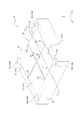
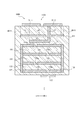
- FIG. 1 is a perspective view of a resonant structure 10 according to an embodiment.
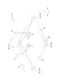
- FIG. 2 is a perspective view of the resonant structure 10 shown in FIG. 1 viewed from the negative direction of the Z axis.
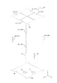
- FIG. 3 is a perspective view in which a part of the resonant structure 10 shown in FIG. 1 is exploded.
- FIG. 4 is a cross-sectional view of the resonant structure 10 taken along the line L1-L1 shown in FIG.
- the positive direction of the X-axis and the negative direction of the X-axis are collectively described as “X direction”.
- the positive direction of the Y axis and the negative direction of the Y axis are collectively described as “Y direction”.
- the positive direction of the Z-axis and the negative direction of the Z-axis are collectively described as “Z direction”.
- the first plane is shown as the XY plane in the XYZ coordinate system.
- the first direction is shown as the X direction.
- the second direction intersecting the first direction is shown as the Y direction.
- the resonance structure 10 is configured to resonate at one or a plurality of resonance frequencies. As shown in FIGS. 1 and 2, the resonance structure 10 includes a base body 20, a conductor portion 30, and a ground conductor 40. The resonance structure 10 has connection conductors 60-1, 60-2, 60-3, 60-4. In the following, if the connection conductors 60-1 to 60-4 are not particularly distinguished, the connection conductors 60-1 to 60-4 will be collectively referred to as "connection conductor 60". The number of connecting conductors 60 included in the resonant structure 10 is not limited to four. The resonant structure 10 may have the first predetermined number of connection conductors 60. The first predetermined number is three or more. The resonant structure 10 may include at least one of the first power supply line 51 and the second power supply line 52 illustrated in FIG. 1.
- the base body 20 may include a dielectric material.
- the relative permittivity of the base body 20 may be appropriately adjusted according to the desired resonance frequency of the resonant structure 10.
- the base body 20 is configured to support the conductor portion 30 and the ground conductor 40.
- the base body 20 is a quadrangular prism, as shown in FIGS. However, the base body 20 may have any shape as long as it can support the conductor portion 30 and the ground conductor 40.
- the base body 20 has an upper surface 21 and a lower surface 22, as shown in FIG. The upper surface 21 and the lower surface 22 spread along the XY plane.
- the conductor portion 30 shown in FIG. 1 may include a conductive material.
- the conductor portion 30, the ground conductor 40, the first power supply line 51, the second power supply line 52, and the connection conductor 60 may include the same conductive material or may include different conductive materials.
- the conductor portion 30 shown in FIG. 1 is configured to function as a part of the resonator.
- the conductor portion 30 extends along the XY plane.
- the conductor portion 30 has a substantially square shape including two sides substantially parallel to the X direction and two sides substantially parallel to the Y direction. However, the conductor portion 30 may have any shape.
- the conductor portion 30 is located on the upper surface 21 of the base body 20.
- the resonant structure 10 can exhibit artificial magnetic wall characteristics with respect to electromagnetic waves of a predetermined frequency that are incident on the upper surface 21 of the base body 20 on which the conductor portion 30 is located.
- “Artificial Magnetic Conductor Character” means the characteristic of a surface where the phase difference between the incident wave that is incident and the reflected wave that is reflected is 0 degree. On the surface having the artificial magnetic wall characteristic, the phase difference between the incident wave and the reflected wave is ⁇ 90 degrees to +90 degrees in the frequency band.
- the conductor portion 30 includes a gap Sx and a gap Sy.
- the gap Sx extends along the Y direction.
- the gap Sx is located near the center of the side of the conductor portion 30 substantially parallel to the X direction in the X direction.
- the gap Sy extends along the X direction.
- the gap Sy is located near the center of the side of the conductor portion 30 substantially parallel to the Y direction in the Y direction.
- the width of the gap Sx and the width of the gap Sy may be appropriately adjusted according to the desired resonance frequency of the resonant structure 10.
- the conductor portion 30 includes first conductors 31-1, 31-2, 31-3, 31-4 as shown in FIG.
- first conductor 31 when the first conductors 31-1 to 31-4 are not particularly distinguished, the first conductors 31-1 to 31-4 are collectively referred to as “first conductor 31”.
- the number of the first conductors 31 included in the conductor portion 30 is not limited to four.
- the conductor portion 30 may include any number of first conductors 31.
- the first conductor 31 shown in FIG. 1 may be a flat conductor.
- the first conductor 31 is of a substantially square shape having the same shape and including two sides substantially parallel to the X direction and two sides substantially parallel to the Y direction.
- each of the first conductors 31-1 to 31-4 may have any shape.
- Each of the first conductors 31-1 to 31-4 is configured to be connected to one of the different connection conductors 60-1 to 60-4 as shown in FIGS. 1 and 3.
- the first conductor 31 may include a connecting portion 31a at one corner of the four corners of the square.
- the connection portion 31a is configured to be connected to the connection conductor 60.
- the first conductor 31 may omit the connecting portion 31a.
- Part of the first conductor 31 may include the connecting portion 31a, and the other part may omit the connecting portion 31a.
- the connecting portion 31a shown in FIG. 1 has a circular shape. However, the connecting portion 31a is not limited to a circular shape and may have any shape.
- Each of the first conductors 31-1 to 31-4 spreads along the XY plane. As shown in FIG. 1, each of the first conductor 31-1 to the first conductor 31-4 can be arranged in a square lattice shape along the X direction and the Y direction.
- the first conductor 31-1 and the first conductor 31-2 are arranged along the X direction of a square lattice along the X direction and the Y direction.
- the first conductor 31-3 and the first conductor 31-4 are arranged along the X direction of the square lattice along the X direction and the Y direction.
- the first conductor 31-1 and the first conductor 31-4 are arranged along the Y direction of the square lattice along the X direction and the Y direction.
- the first conductor 31-2 and the first conductor 31-3 are arranged along the Y direction of the square lattice along the X direction and the Y direction.
- the first conductor 31-1 and the first conductor 31-3 are arranged along the first diagonal direction of the square lattice along the X and Y directions.
- the first diagonal direction is a direction inclined by 45 degrees from the positive direction of the X axis toward the positive direction of the Y axis.
- the first conductor 31-2 and the first conductor 31-4 are arranged along the second diagonal line of the square lattice along the X direction and the Y direction.
- the second diagonal direction is a direction inclined by 135 degrees from the positive direction of the X axis toward the positive direction of the Y axis.
- the grid in which the first conductors 31-1 to 31-4 are arranged is not limited to the square grid.
- the first conductor 31-1 to the first conductor 31-4 may be arranged arbitrarily.
- the first conductors 31 may be arranged in a diagonal grid pattern, a rectangular grid pattern, a triangular grid pattern, and a hexagonal grid pattern.
- the first conductor 31 may include a portion configured to be capacitively connected to the different first conductor 31 by having a gap between the different first conductor 31.
- the first conductor 31-1 and the first conductor 31-2 can be configured to be capacitively connected by having a gap Sx between them.
- the first conductor 31-3 and the first conductor 31-4 can be configured to be capacitively connected by having a gap Sx between them.
- the first conductor 31-1 and the first conductor 31-4 can be configured to be capacitively connected by having a gap Sy between them.
- the first conductor 31-2 and the first conductor 31-3 can be configured to be capacitively connected by having a gap Sy between them.
- the first conductor 31-1 and the first conductor 31-3 can be configured to be capacitively connected by having the gap Sx and the gap Sy between them.
- the first conductor 31-1 and the first conductor 31-3 may be configured to be capacitively connected via the first conductor 31-2 and the first conductor 31-4.
- the first conductor 31-2 and the first conductor 31-4 can be configured to be capacitively connected by having the gap Sx and the gap Sy between them.
- the first conductor 31-2 and the first conductor 31-4 may be configured to be capacitively connected via the first conductor 31-1 and the first conductor 31-3.
- the resonant structure 10 may have the capacitive elements C1 and C2 in the gap Sx.
- the resonant structure 10 may have the capacitive elements C3 and C4 in the gap Sy.
- the capacitive elements C1 to C4 may be chip capacitors or the like.
- the capacitive element C1 is located between the first conductor 31-1 and the first conductor 31-2 in the gap Sx.
- the capacitive element C1 is configured to capacitively connect the first conductor 31-1 and the first conductor 31-2.
- the capacitive element C2 is located between the first conductor 31-3 and the first conductor 31-4 in the gap Sx.
- the capacitive element C2 is configured to capacitively connect the first conductor 31-3 and the first conductor 31-4.
- the capacitive element C3 is located between the first conductor 31-2 and the first conductor 31-3 in the gap Sy.
- the capacitive element C3 is configured to capacitively connect the first conductor 31-2 and the first conductor 31-3.
- the capacitive element C4 is located between the first conductor 31-1 and the first conductor 31-4 in the gap Sy.
- the capacitive element C4 is configured to capacitively connect the first conductor 31-1 and the first conductor 31-4.
- the positions of the capacitive elements C1 and C2 in the gap Sx and the positions of the capacitive elements C3 and C4 in the gap Sy may be appropriately adjusted according to the desired resonance frequency of the resonant structure 10.
- the capacitance values of the capacitive elements C1 to C4 may be appropriately adjusted according to the desired resonance frequency of the resonant structure 10. When the capacitance value of the capacitive elements C1 to C4 is increased, the resonant frequency of the resonant structure 10 can be lowered. When the capacitance value of the capacitive elements C1 to C4 is reduced, the resonant frequency of the resonant structure 10 can be increased.
- the ground conductor 40 shown in FIG. 2 may include a conductive material.
- the ground conductor 40 is configured to provide a reference electric potential in the resonant structure 10.
- the ground conductor 40 may be configured to be connected to the ground of the device including the resonant structure 10.
- the ground conductor 40 may be a flat conductor.
- the ground conductor 40 is located on the lower surface 22 of the base 20, as shown in FIG. 2.
- Various components of the device including the resonant structure 10 may be located on the negative side of the ground conductor 40 in the Z-axis direction.
- the metal plate may be located on the negative side of the ground conductor 40 in the Z-axis direction.
- the resonant structure 10 as an antenna may be configured to maintain the radiation efficiency at a predetermined frequency even when the metal plate is located on the negative side of the ground conductor 40 in the Z-axis direction.
- the ground conductor 40 extends along the XY plane, as shown in FIGS. 2 and 3.
- the ground conductor 40 is located apart from the conductor portion 30.
- the base body 20 is interposed between the ground conductor 40 and the conductor portion 30.
- the ground conductor 40 faces the conductor portion 30 in the Z direction.
- the ground conductor 40 has a shape corresponding to the shape of the conductor portion 30.
- the ground conductor 40 has a substantially square shape corresponding to the substantially square conductor portion 30.
- the ground conductor 40 may have any shape according to the shape of the conductor portion 30.
- the ground conductor 40 includes a connecting portion 40a at each of the four corners of the square.
- the connection portion 40a is configured to be connected to the connection conductor 60.
- the ground conductor 40 may omit a part of the connecting portion 40a.
- the connecting portion 40a shown in FIG. 2 has a circular shape. However, the connecting portion 40a is not limited to a circular shape and may have any shape.
- the first power supply line 51 and the second power supply line 52 shown in FIG. 3 may include a conductive material.
- Each of the first feeder line 51 and the second feeder line 52 may be a through-hole conductor, a via conductor, or the like.
- the first feeder line 51 and the second feeder line 52 may be located in the base body 20.
- the first power supply line 51 shown in FIG. 3 is configured to be electromagnetically connected to the first conductor 31-1 included in the conductor section 30 shown in FIG.
- electroagnetic connection may be an electrical connection or a magnetic connection.
- the first feeder line 51 can extend from the opening 41 of the ground conductor 40 shown in FIG. 2 to an external device or the like.
- the first power supply line 51 is configured to supply power to the conductor portion 30 via the first conductor 31-1.
- the first power supply line 51 is configured to supply power from the conductor portion 30 to the external device or the like via the first conductor 31-1.
- the second power supply line 52 shown in FIG. 3 is configured to be electromagnetically connected to the first conductor 31-2 included in the conductor section 30 shown in FIG.
- the second power supply line 52 is configured to be electromagnetically connected to the conductor portion 30 at a position different from the first power supply line 51.
- the second power supply line 52 can extend from the opening 42 of the ground conductor 40 to an external device or the like.
- the second power supply line 52 is configured to supply power to the conductor portion 30 via the first conductor 31-2.
- the second power supply line 52 is configured to supply the power from the conductor portion 30 via the first conductor 31-2 to an external device or the like.
- the connecting conductor 60 shown in FIG. 3 may include a conductive material.
- the connection conductor 60 extends from the ground conductor 40 toward the conductor portion 30.
- the connecting conductor 60 can be a through-hole conductor, a via conductor, or the like.
- Each of the connection conductors 60-1 to 60-4 is configured to connect the first conductor 31-1 to 31-4 and the ground conductor 40, respectively.
- connection conductor 60-1 and the connection conductor 60-4 shown in FIG. 1 can be one set.
- the connection conductor 60-2 and the connection conductor 60-3 can be one set.
- the set of connection conductors 60-1 and 60-4 and the set of connection conductors 60-2 and 60-3 form a first connection pair arranged along the X direction as the first direction.
- the set of the connection conductors 60-1 and 60-4 and the set of the connection conductors 60-2 and 60-3 are the first set of the first conductors 31-1 and 31-4 and the first set of the first conductors 31 arranged in a square lattice.
- the first connection pair is arranged along the X direction in which the set of conductors 31-2 and 31-3 is arranged.
- the resonant structure 10 is configured to resonate at the first frequency along the first path parallel to the X direction.
- the first path is a part of the first current path passing through the set of the connection conductors 60-1 and 60-4 and the set of the connection conductors 60-2 and 60-3 of the first connection pair.
- the first current path includes a ground conductor 40, a set of first conductors 31-1 and 31-4, a set of first conductors 31-2 and 31-3, and a connection conductor 60-1 of a first connection pair.
- a set of 60-4 and a set of connecting conductors 60-2, 60-3 are included.
- a part of the first current path is shown as a current path I.
- the set of the connection conductors 60-1 and 60-4 and the set of the connection conductors 60-2 and 60-3 are It can be configured to function as a pair of electrical walls.
- the current flowing through the first current path including the first path causes the connection conductors 60-1 and 60-2 to have
- the set and the set of connection conductors 60-3 and 60-4 may be configured to function as a pair of magnetic walls.
- connection conductors 60-1, 60-4 and the set of the connection conductors 60-2, 60-3 function as a pair of electric walls
- the set of the connection conductors 60-1, 60-2 and the connection conductor 60-3 Since the set of 60-4 functions as a pair of magnetic walls, the resonant structure 10 polarizes along the first path of the first frequency incident from the outside onto the upper surface 21 of the base body 20 on which the conductor portion 30 is located. It can be configured to exhibit artificial magnetic wall characteristics with respect to generated electromagnetic waves.
- the resonance structure 10 is configured as an antenna to radiate a polarized electromagnetic wave along a first path parallel to the X direction when power is supplied from the first power supply line 51 to the conductor portion 30. obtain.
- connection conductor 60-1 and the connection conductor 60-2 can be one set.
- the connection conductor 60-3 and the connection conductor 60-4 can be one set.
- the set of connection conductors 60-1 and 60-2 and the set of connection conductors 60-3 and 60-4 form a second connection pair arranged along the Y direction as the second direction.
- the set of the connection conductors 60-1 and 60-2 and the set of the connection conductors 60-3 and 60-4 are the first set of the first conductors 31-1 and 31-2 and the first set of the first conductors 31 arranged in a square lattice.
- a second connection pair is formed along the Y direction in which the set of conductors 31-3 and 31-4 is arranged.
- the resonance structure 10 is configured to resonate at the second frequency along the second path parallel to the Y direction.
- the second path is a part of the second current path passing through the set of the connection conductors 60-1 and 60-2 and the set of the connection conductors 60-3 and 60-4 of the second connection pair.
- the second current path includes a ground conductor 40, a set of first conductors 31-1 and 31-2, a set of first conductors 31-3 and 31-4, and a connection conductor 60-1 of a second connection pair.
- a set of 60-2 and a set of connecting conductors 60-3 and 60-4 are included.
- the set of the connection conductors 60-1 and 60-2 and the set of the connection conductors 60-3 and 60-4 are , Can be configured to function as a pair of electrical walls.
- the set of the connection conductors 60-2 and 60-3 and the connection conductor are viewed from the current flowing through the second current path including the second path.
- the set of 60-1 and 60-4 may be configured to function as a pair of magnetic walls.
- connection conductors 60-1 and 60-2 and the set of the connection conductors 60-3 and 60-4 function as a pair of electric walls
- the set of the connection conductors 60-2 and 60-3 and the connection conductor 60-1 Since the set of 60-4 functions as a pair of magnetic walls, the resonant structure 10 polarizes along the second path of the second frequency incident from the outside onto the upper surface 21 of the base body 20 on which the conductor portion 30 is located. It can be configured to exhibit artificial magnetic wall characteristics with respect to generated electromagnetic waves.
- the resonance structure 10 can radiate a polarized electromagnetic wave along the second path substantially parallel to the Y direction when power is supplied from the second power supply line 52 to the conductor portion 30.
- the conductor portion 30 has a substantially square shape.
- the length of the first current path and the length of the second current path can be equal.
- the first frequency and the second frequency can be equal.
- the resonant structure 10 may be configured so that the first frequency and the second frequency are different depending on the application and the like.
- the resonant structure 10 by making the conductor portion 30 into a rectangular shape, the length of the first current path is made different from the length of the second current path so that the first frequency and the second frequency are made different. May be configured to.
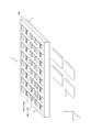
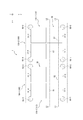
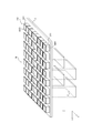
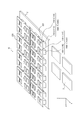
- FIG. 5 is a perspective view of the array antenna 1 according to the embodiment.
- FIG. 6 is an enlarged view of the array antenna 1 in the range A shown in FIG.
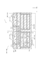
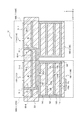
- FIG. 7 is a sectional view of the array antenna 1 taken along the line L2-L2 shown in FIG.
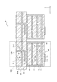
- FIG. 8 is a sectional view of the array antenna 1 taken along the line L3-L3 shown in FIG.
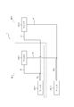
- FIG. 9 is a circuit diagram of the antenna elements 100-1 and 100-2 shown in FIG.
- the xyz coordinate system is used.
- the positive direction of the x-axis and the negative direction of the x-axis are not particularly distinguished, the positive direction of the x-axis and the negative direction of the x-axis are collectively described as “x direction”.
- the positive direction of the y-axis and the negative direction of the y-axis are not particularly distinguished, the positive direction of the y-axis and the negative direction of the y-axis are collectively described as “y direction”.
- the positive direction of the z axis and the negative direction of the z axis are collectively described as “z direction”.
- the fourth direction is shown as the x direction.
- the fifth direction intersecting the fourth direction is shown as the y direction.
- the eighth direction is shown as the z direction.
- the xyz coordinate system shown in FIG. 5 and the like may correspond to the XYZ coordinate system shown in FIG. 1 and the like.
- the fourth direction, that is, the x direction shown in FIG. 5 may correspond to the X direction shown in FIG. 1 that is the first direction or the Y direction shown in FIG. 1 that is the second direction.
- the array antenna 1 shown in FIG. 5 may be located on the circuit board 2.
- the array antenna 1 may be configured to be connected to the integrated circuit 3 via the circuit board 2.
- the integrated circuit 3 may be an RFIC (Radio Frequency Integrated Circuit).
- the array antenna 1 may be directly connected to the integrated circuit 3 without the circuit board 2. In the configuration in which the antenna 1 is directly connected to the integrated circuit 3, the array antenna 1 does not have to be located on the circuit board 2.
- the array antenna 1 includes an antenna element 100-1 (first antenna element), an antenna element 100-2 (second antenna element), and an antenna substrate 200.
- antenna elements 100-1 and 100-2 are not particularly distinguished, the antenna elements 100-1 and 100-2 are collectively referred to as "antenna element 100".
- the array antenna 1 may include any number of antenna elements 100.
- the plurality of antenna elements 100 are arranged in a square lattice along the x and y directions.
- the grid in which the plurality of antenna elements 100 are arranged is not limited to the square grid.
- the plurality of antenna elements 100 may be arranged arbitrarily.
- the plurality of antenna elements 100 may be arranged in a diagonal grid pattern, a rectangular grid pattern, a triangular grid pattern, and a hexagonal grid pattern.
- the plurality of antenna elements 100 may be integrated with the antenna substrate 200 as shown in FIGS. 7 and 8.
- the antenna element 100-1 and the antenna element 100-2 can be arranged along the x direction as shown in FIG.
- the antenna element 100-1 and the antenna element 100-2 may be adjacent to each other.
- the antenna element 100-1 has an antenna 110-1 (first antenna) and a filter 120-1 (first filter).
- the antenna element 100-2 has an antenna 110-2 (second antenna) and a filter 120-2 (second filter).
- antennas 110-1 and 110-2 are not particularly distinguished, the antennas 110-1 and 110-2 are collectively referred to as “antenna 110”.
- filters 120-1 and 120-2 are not particularly distinguished, the filters 120-1 and 120-2 are collectively referred to as “filter 120”.
- the resonance structure 10 shown in FIG. 1 is adopted as the antenna 110.
- the antenna 110 includes a conductor portion 30 including the first conductors 31-1 to 31-4, a ground conductor 40, a first feeder line 51, and a second feeder line 52. It has connection conductors 60-1 to 60-4.
- the ground conductor 40 of the antenna 110-1 and the ground conductor 40 of the antenna 110-2 may be integrated.
- the first feed line 51 of the antenna 110-1 and the first feed line 51 of the antenna 110-2 are configured to be electrically connected to the wiring 51a.
- the wiring 51a is located between the ground conductor 40 and the ground conductor 121 of the filter 120.
- the wiring 51a is configured to be electromagnetically connected to the filter 120-1.
- the wiring 51a is configured to be magnetically connected to the filter 12-1.
- the wiring 51a covers the opening 121a of the ground conductor 121 of the filter 120-1 on the xy plane.
- the wiring 51a may be configured to be magnetically connected to the filter 120-1 by covering the opening 121a of the ground conductor 121 of the filter 120-1.
- the antenna 110-1 is connected to the filter 120- via the wiring 51a and the first feeder line 51 of the antenna 110-1 as shown in FIG. 1 may be configured to be electromagnetically connected. Since the wiring 51a is electromagnetically connected to the filter 120-1, the antenna 110-2 is electromagnetically connected to the filter 120-1 via the wiring 51a and the first feeder line 51 of the antenna 110-2. Can be configured to.
- the antenna 110-1 is configured to radiate the electric power supplied from the filter 120-1 shown in FIG. 9 via the first power supply line 51 as an electromagnetic wave polarized in the x direction shown in FIG. There is.
- the antenna 110-1 supplies an electromagnetic wave, which is polarized from the outside to the antenna 110-1 along the x direction, to the filter 120-1 via the first power supply line 51 shown in FIG. Is configured.
- the antenna 110-2 is configured to radiate the electric power supplied from the filter 120-1 shown in FIG. 9 via the first feeder line 51 as an electromagnetic wave polarized in the x direction shown in FIG. There is.
- the antenna 110-2 supplies an electromagnetic wave, which is polarized along the x direction, out of electromagnetic waves entering the antenna 110-2 from the outside, to the filter 120-1 via the first power supply line 51 shown in FIG. Is configured.
- the second power supply line 52 of the antenna 110-1 and the second power supply line 52 of the antenna 110-2 are configured to be electrically connected to the wiring 52a.
- the wiring 52a is located between the ground conductor 40 and the ground conductor 121 of the filter 120.
- the wiring 52a is configured to be electromagnetically connected to the filter 120-2.
- the wiring 52a is configured to be magnetically connected to the filter 120-2.
- the wiring 52a covers the opening 121a of the ground conductor 121 of the filter 120-2 on the xy plane.
- the wiring 52a may be configured to be magnetically connected to the filter 120-2 by covering the opening 121a of the ground conductor 121 of the filter 120-2.
- the antenna 110-1 is connected to the filter 120- via the wiring 52a and the second power supply line 52 of the antenna 110-1 as shown in FIG. 2 may be configured to be electromagnetically connected. Since the wiring 52a is electromagnetically connected to the filter 120-2, the antenna 110-2 is electromagnetically connected to the filter 120-2 via the wiring 52a and the second power supply line 52 of the antenna 110-2. Can be configured to.
- the antenna 110-1 is configured to radiate the electric power supplied from the filter 120-2 shown in FIG. 9 through the second power supply line 52 as an electromagnetic wave polarized in the y direction shown in FIG. There is.
- the antenna 110-1 supplies an electromagnetic wave, which is polarized along the y direction, out of electromagnetic waves entering the antenna 110-1 from the outside, to the filter 120-2 via the second power supply line 52 shown in FIG. Is configured.
- the antenna 110-2 is configured to radiate the electric power supplied from the filter 120-2 shown in FIG. 9 via the second power supply line 52 as an electromagnetic wave polarized in the y direction shown in FIG. There is.
- the antenna 110-2 supplies an electromagnetic wave, which is polarized along the y direction, of the electromagnetic waves incident on the antenna 110-2 from the outside to the filter 120-2 via the second power supply line 52 shown in FIG. Is configured.
- the filter 120-1 is configured to be electromagnetically connected to the first feeding line 51 of the antenna 110-1 and the first feeding line 51 of the antenna 110-2 via the wiring 51a. Has been done.
- the filter 120-1 is located so as to overlap with the ground conductor 40 of the antenna 110-1.
- the position of the filter 120-1 in the xy plane may be the same as or near the position of the antenna 110-1 in the xy plane.
- the filter 120-1 may be located in the antenna substrate 200.
- the filter 120-2 is configured to be electromagnetically connected to the second power supply line 52 of the antenna 110-1 and the second power supply line 52 of the antenna 110-2 via the wiring 52a. Has been done.
- the filter 120-2 is located so as to overlap with the ground conductor 40 of the antenna 110-2.
- the position of the filter 120-2 in the xy plane may be the same as or near the position of the antenna 110-2 in the xy plane.
- the filter 120-2 may be located in the antenna substrate 200.
- the filter 120 is a laminated waveguide type filter. However, the filter 120 is not limited to the laminated waveguide type filter.
- the filter 120 may have any structure depending on the application of the array antenna 1. As shown in FIGS. 7 and 8, the filter 120 includes a ground conductor 121, a wiring 122, conductors 123, 124 and 125, and conductors 126 and 127. Filter 120 may include any number of conductors 123 or the like.
- Ground conductor 121 may include a conductive material.
- the members included in the ground conductor 121, the wiring 122, the conductors 123 to 125, the conductors 126 and 127, and the antenna 110 may include the same conductive material or different conductive materials. As shown in FIGS. 7 and 8, the ground conductor 121 includes an opening 121a.
- the ground conductor 121 of the filter 120-1 and the ground conductor 121 of the filter 120-2 may be integrated.
- the ground conductor 121 of the filter 120-1 is superposed on the ground conductor 40 of the antenna 110-1.
- the opening 121a of the ground conductor 121 of the filter 120-1 faces the wiring 51a.
- the ground conductor 121 of the filter 120-2 is superposed on the ground conductor 40 of the antenna 110-2.
- the opening 121a of the ground conductor 121 of the filter 120-2 faces the wiring 52a.
- the wiring 122 shown in FIGS. 7 and 8 may include a conductive material.
- the wiring 122 covers the opening 125a of the conductor 125 on the xy plane.
- the wiring 122 is configured to be electrically connected to the circuit board 2 shown in FIG.
- the wiring 122 is configured to be electrically connected to the integrated circuit 3 via the circuit board 2 shown in FIG. In the configuration in which the array antenna 1 shown in FIG. 5 is directly connected to the integrated circuit 3, the wiring 122 may be configured to be electrically directly connected to the integrated circuit 3.
- the conductors 123 to 125 may include a conductive material.
- the conductors 123 to 125 are configured to function as a part of the laminated waveguide.
- Each of the conductors 123, 124, 125 includes an opening 123a, 124a, 125a, respectively.
- the conductors 123 to 125 are located so that the openings 123a to 125a face each other in the z direction.
- Each of the conductors 123 to 125 is configured to be electromagnetically coupled through the respective opening 123a to 125a.
- the conductor 126 shown in FIGS. 7 and 8 extends in the z direction near one end of the filter 120.
- the plurality of conductors 126 arranged in the y direction are configured to be electrically connected via the conductors 123 to 125 extending in the y direction.
- the conductor 127 illustrated in FIGS. 7 and 8 extends along the z direction near the other end of the filter 120.
- the plurality of conductors 126 arranged in the y direction are configured to be electrically connected via the conductors 123 to 125 extending in the y direction.
- the antenna substrate 200 shown in FIGS. 7 and 8 may include a dielectric material, the same as or similar to the base body 20 shown in FIG. A plurality of antenna elements 100 are arranged on the antenna substrate 200.
- the antenna element 100 includes the antenna 110 and the filter 120 that is positioned so as to be superposed on the ground conductor 40 of the antenna 110, as shown in FIG. 7.
- the antenna element 100 can be downsized. Therefore, an improved antenna element 100 may be provided.
- the array antenna 1 can be downsized by downsizing the antenna element 100. Therefore, an improved array antenna 1 can be provided.
- FIG. 10 is a sectional view of an array antenna 1A according to another embodiment.
- FIG. 11 is a circuit diagram of the antenna element 100A shown in FIG.
- Array antenna 1A is another embodiment of array antenna 1 shown in FIG.
- the sectional view shown in FIG. 10 corresponds to the sectional view taken along line L3-L3 shown in FIG.
- the array antenna 1A has a plurality of antenna elements 100A and an antenna substrate 200.
- the external configuration of the array antenna 1A is the same as or similar to that of the array antenna 1 shown in FIG.
- the plurality of antenna elements 100A may be arranged in a square lattice pattern on the antenna substrate 200, the same as or similar to the antenna element 100 shown in FIG.
- the antenna element 100A has an antenna 110A and a filter 120, as shown in FIGS.
- the first feeding line 51 of the antenna 110A and the second feeding line 52 of the antenna 110A are configured to be electrically connected to the wiring 53.
- the wiring 53 is located between the ground conductor 40 and the ground conductor 121 of the filter 120.
- the wiring 53 is configured to be electromagnetically connected to the filter 120.
- the wiring 53 is configured to be magnetically connected to the filter 120.
- the wiring 53 covers the opening 121a of the ground conductor 121 of the filter 120.
- the wiring 53 may be configured to be magnetically connected to the filter 120 by covering the opening 121a of the ground conductor 121 of the filter 120.
- the antenna 110A is electromagnetically connected to the filter 120 via the first power supply line 51 and the second power supply line 52, as shown in FIG. 11. Can be configured to.
- the antenna 110A is configured to radiate the electric power supplied from the filter 120 via the first power supply line 51 and the second power supply line 52 as an electromagnetic wave.
- the antenna 110A is configured to supply an electromagnetic wave incident on the antenna 110A from the outside to the filter 120 via the first power supply line 51 and the second power supply line 52.
- the filter 120 is configured to be electromagnetically connected to the first power supply line 51 and the second power supply line 52 of the antenna 110A via the wiring 53.
- FIG. 12 is a perspective view of the array antenna 1B according to the embodiment.
- FIG. 13 is a sectional view of the array antenna 1B shown in FIG. The sectional view shown in FIG. 13 corresponds to the sectional view taken along the line L3-L3 shown in FIG.
- the array antenna 1B shown in FIG. 12 is configured to be electrically connected to the integrated circuit 3 via the circuit board 2 in the same or similar manner to the configuration shown in FIG.
- the array antenna 1B has a plurality of antenna elements 100B and an antenna substrate 210.
- the antenna element 100B has an antenna 110A and a filter 130, as shown in FIG.
- the circuit configuration of the antenna element 100B can be the same as or similar to the configuration shown in FIG.
- the antenna 110A may be configured to be electromagnetically connected to the filter 130 via the first power supply line 51 and the second power supply line.
- the first feeding line 51 of the antenna 110A and the second feeding line 52 of the antenna 110A are configured to be electrically connected to the wiring 53.
- the wiring 53 is located between the ground conductor 40 and the ground conductor 131 of the filter 130.
- the wiring 53 is configured to be electromagnetically connected to the filter 130, which is the same as or similar to the structure shown in FIG. Since the wiring 53 is electromagnetically connected to the filter 130, the antenna 110A can be configured to be electromagnetically connected to the filter 130 via the first power supply line 51 and the second power supply line 52.
- the antenna 110A is configured to radiate the electric power supplied from the filter 130 via the first power supply line 51 and the second power supply line 52 as an electromagnetic wave.
- the antenna 110A is configured to supply an electromagnetic wave incident on the antenna 110A from the outside to the filter 130 via the first power supply line 51 and the second power supply line 52.
- the filter 130 is configured to be electromagnetically connected to the first feeding line 51 and the second feeding line 52 of the antenna 110A via the wiring 53.
- the filter 130 is located so as to overlap with the ground conductor 40 of the antenna 110A.
- the position of the filter 130 in the xy plane may be the same as or near the position of the antenna 110A in the xy plane.
- the filter 130 may be located in the substrate portion 211 of the antenna substrate 210.
- the filter 130 is a dielectric filter. However, the filter 130 is not limited to the dielectric filter.
- the filter 130 may have an arbitrary structure depending on the application of the array antenna 1B and the like. As shown in FIG. 13, the filter 130 includes a ground conductor 131, a wiring 132, three dielectric blocks 133, conductors 134, 135 and 136, and conductors 137 and 138.
- the filter 130 may include any number of dielectric blocks 133.
- the ground conductor 131 may include a conductive material.
- the members included in the ground conductor 131, the wiring 132, the conductors 134 to 136, the conductors 137 and 138, and the antenna 110A may include the same conductive material or different conductive materials.
- the ground conductor 131 includes an opening 131a. The opening 131 a of the ground conductor 131 faces the wiring 53.
- the wiring 132 may include a conductive material.
- the wiring 132 covers the opening 136a of the conductor 136 on the xy plane.
- the wiring 132 is configured to be electrically connected to the circuit board 2 shown in FIG.
- the wiring 132 is configured to be electrically connected to the integrated circuit 3 via the circuit board 2 shown in FIG. In the configuration in which the array antenna 1B shown in FIG. 12 is directly connected to the integrated circuit 3, the wiring 132 may be configured to be electrically directly connected to the integrated circuit 3.
- the dielectric block 133 may include a dielectric material.
- the dielectric constant of the dielectric block 133 may be appropriately selected according to the application of the array antenna 1B and the like.
- Conductors 134-136 may include conductive materials. Each of the conductors 134, 135, 136 includes an opening 134a, 135a, 136a, respectively. The conductors 134 to 136 are located so that the openings 134a to 136a face each other in the z direction. Each of the conductors 134 to 136 is configured to be electromagnetically coupled through the respective opening 134a to 136a.
- the conductors 137 and 138 may include a conductive material.
- the conductor 137 is located on one surface of the dielectric block 133 of the two surfaces substantially parallel to the zy plane included in the dielectric block 133.
- the conductor 138 is located on the other surface of the dielectric block 133 among the two surfaces substantially parallel to the zy plane included in the dielectric block 133.
- Each of the conductors 137 and 138 extends along the zy plane.
- the antenna substrate 210 shown in FIG. 12 may include a dielectric material, the same as or similar to the base body 20 shown in FIG.
- the antenna substrate 210 includes a plurality of substrate parts 211. As shown in FIGS. 12 and 13, one antenna element 100B is arranged on the board portion 211. However, an arbitrary number of antenna elements 100B may be arranged on the substrate portion 211 shown in FIG.
- the board parts 211 may be arranged appropriately in the array antenna 1B depending on the manner in which the antenna elements 100B are arranged.
- the plurality of substrate parts 211 may be arranged in a square lattice shape along the x direction and the y direction.
- the plurality of substrate parts 211 may be arranged along the x direction or the y direction.
- FIG. 14 is a perspective view of the array antenna 1C according to the embodiment.
- FIG. 15 is a sectional view of the array antenna 1C shown in FIG. 14 (No. 1).
- the cross-sectional view shown in FIG. 15 corresponds to the cross-sectional view taken along line L2-L2 shown in FIG.
- FIG. 16 is a cross-sectional view of the array antenna 1C shown in FIG. 14 (No. 2).
- the sectional view shown in FIG. 16 corresponds to the sectional view taken along line L3-L3 shown in FIG.
- the array antenna 1C shown in FIG. 14 is electrically connected to the integrated circuit 3 via the circuit board 2.
- the array antenna 1C has an antenna element 100C-1 (first antenna element) and an antenna element 100C-2 (second antenna element), and an antenna substrate 220.
- antenna elements 100C-1 and 100C-2 are not particularly distinguished, the antenna elements 100C-1 and 100C-2 are collectively referred to as "antenna element 100C".
- the array antenna 1 may include any number of antenna elements 100C.
- the plurality of antenna elements 100C are arranged in a grid on the antenna substrate 220.
- four antenna elements 100C are arranged in a square lattice pattern on the substrate portion 221 of the antenna substrate 220.
- the antenna element 100C-1 includes an antenna 110-1 and a filter 140-1.
- the antenna element 100C-2 includes an antenna 110-2 and a filter 140-2.
- the filters 140-1 and 140-2 are not particularly distinguished, the filters 140-1 and 140-2 are collectively referred to as “filter 140”.
- the circuit configuration of the antenna elements 100C-1 and 100C-2 may be the same as or similar to the circuit configuration shown in FIG.
- the antenna elements 100C-1 and 100C-2 are configured to be electromagnetically connected to the filter 140-1 via the first power supply line 51 and the wiring 51a.
- the antenna elements 100C-1 and 100C-2 are configured to be electromagnetically connected to the filter 140-2 via the second power supply line 52 and the wiring 52a.
- the filter 140-1 is configured to be electromagnetically connected to the first power supply line 51 of the antenna 110-1 and the first power supply line 51 of the antenna 110-2 via the wiring 51a. Has been done.
- the filter 140-1 is located so as to overlap with the ground conductor 40 of the antenna 110-1.
- the position of the filter 140-1 in the xy plane may be the same as or near the position of the antenna 110-1 in the xy plane.
- the filter 140-2 is configured to be electromagnetically connected to the second power supply line 52 of the antenna 110-1 and the second power supply line 52 of the antenna 110-2 via the wiring 52a. Has been done.
- the filter 140-2 is located so as to overlap with the ground conductor 40 of the antenna 110-2.
- the position of the filter 140-2 in the xy plane may be the same as or near the position of the antenna 110-2 in the xy plane.
- the filter 140 is a dielectric filter. However, the filter 140 is not limited to the dielectric filter.
- the filter 140 may have an arbitrary structure depending on the application of the array antenna 1C and the like. As shown in FIGS. 15 and 16, the filter 140 includes a ground conductor 141, a wiring 142, three dielectric blocks 143, conductors 144, 145, 146, and conductors 147, 148. Filter 140 may include any number of dielectric blocks 143.
- Ground conductor 141 may include a conductive material.
- the members included in the ground conductor 141, the wiring 142, the conductors 144 to 146, the conductors 147 and 148, and the antenna 110 may include the same conductive material or different conductive materials. As shown in FIGS. 15 and 16, the ground conductor 141 includes an opening 141a.
- the ground conductor 141 of the filter 140-1 is superposed on the ground conductor 40 of the antenna 110-1.
- the opening 141a of the ground conductor 141 of the filter 140-1 faces the wiring 51a.
- the ground conductor 141 of the filter 140-2 is overlaid on the ground conductor 40 of the antenna 110-2.
- the opening 141a of the ground conductor 141 of the filter 140-2 faces the wiring 52a.
- the wiring 142 shown in FIGS. 15 and 16 may include a conductive material.
- the wiring 142 covers the opening 146a of the conductor 146 on the xy plane.
- the wiring 142 is configured to be electrically connected to the circuit board 2 shown in FIG.
- the wiring 142 is configured to be electrically connected to the integrated circuit 3 via the circuit board 2 shown in FIG. In the configuration in which the array antenna 1 shown in FIG. 14 is directly connected to the integrated circuit 3, the wiring 142 may be configured to be electrically directly connected to the integrated circuit 3.
- the dielectric block 143 may include a dielectric material.
- the dielectric constant of the dielectric block 143 may be appropriately selected depending on the application of the array antenna 1C and the like.
- Conductors 144-146 may include conductive materials. Each of conductors 144, 145, 146 includes an opening 144a, 145a, 146a, respectively. The conductors 144 to 146 are located so that the openings 144a to 146a face each other in the z direction. Each of the conductors 144-146 is configured to be electromagnetically coupled through a respective opening 144a-146a.
- the conductors 147 and 148 may include a conductive material.
- the conductor 147 is located on one surface of the dielectric block 143 of the two surfaces substantially parallel to the zy plane included in the dielectric block 143.
- the conductor 148 is located on the other surface of the dielectric block 143 among the two surfaces substantially parallel to the zy plane included in the dielectric block 143.
- Each of the conductors 147 and 148 extends along the zy plane.
- the antenna substrate 220 shown in FIG. 14 may include a dielectric material, the same as or similar to the base body 20 shown in FIG.
- the antenna substrate 220 includes a plurality of substrate parts 221.
- Four antenna elements 100C are arranged on the substrate portion 221.
- the four antenna elements 100C are arranged in a square lattice shape along the x direction and the y direction.
- the number of antenna elements 100C arranged on the substrate portion 221 is not limited to four. At least one antenna element 100C may be located on the board portion 221.
- the board portions 221 may be arranged appropriately in the array antenna 1C depending on the manner in which the antenna elements 100 are arranged. For example, in a configuration in which the antenna elements 100C are arranged in a square lattice shape along the x direction and the y direction, the plurality of substrate parts 221 can be arranged in a square lattice shape along the x direction and the y direction.
- FIG. 17 is a sectional view of an array antenna 1D according to another embodiment.
- the cross-sectional view shown in FIG. 17 corresponds to the cross-sectional view taken along the line L3-L3 shown in FIG.
- the array antenna 1D is another embodiment of the array antenna 1C shown in FIG.
- the array antenna 1D has a plurality of antenna elements 100D and an antenna substrate 220.
- the plurality of antenna elements 100D may be arranged in a square lattice pattern on the substrate portion 221 of the antenna substrate 220, the same or similar to the configuration shown in FIG.
- the antenna element 100D has an antenna 110A and a filter 140.
- the circuit configuration of the antenna element 100D can be the same as or similar to the circuit configuration shown in FIG.
- the antenna 110A is configured to be electromagnetically connected to the filter 140 via the first power supply line 51 and the second power supply line 52.
- the first feeding line 51 of the antenna 110A and the second feeding line 52 of the antenna 110A are configured to be electrically connected to the wiring 53.
- the wiring 53 is located between the ground conductor 40 and the ground conductor 141 of the filter 140.
- the wiring 53 is configured to be electromagnetically connected to the filter 140, the same as or similar to the configuration illustrated in FIG. 10. Since the wiring 53 is electromagnetically connected to the filter 140, the antenna 110 ⁇ / b> A can be configured to be electromagnetically connected to the filter 140 via the first power supply line 51 and the second power supply line 52.
- FIG. 18 is a block diagram of the communication unit 4 according to the embodiment. 19 is a sectional view of the communication unit 4 shown in FIG.
- the communication unit 4 includes an array antenna 1, an integrated circuit 3, a battery 8A, and a sensor 8B as functional blocks.
- the communication unit 4 has an RF module 5, a memory 6A, and a controller 6B as the components of the integrated circuit 3.
- the communication unit 4 includes an array antenna 1, a circuit board 2, and a heat sink 7 in a housing 4A.
- the integrated circuit 3, the battery 8A, and the sensor 8C may be mounted on the circuit board 2.
- the communication unit 4 includes a memory 6A and a controller 6B inside the integrated circuit 3.
- the communication unit 4 may include the memory 6A and the controller 6B outside the integrated circuit 3.
- the communication unit 4 may include any of the array antenna 1A shown in FIG. 1, the array antenna 1B shown in FIG. 12, the array antenna 1C shown in FIG. 14, and the array antenna 1D shown in FIG. 17, instead of the array antenna 1. ..
- the RF module 5 may include a modulation circuit and a demodulation circuit.
- the RF module 5 may be configured to control the power supplied to the array antenna 1 under the control of the controller 6B.
- the RF module 5 may be configured to modulate a baseband signal and supply the baseband signal to the array antenna 1 under the control of the controller 6B.
- the RF module 5 may be configured to modulate the electric signal received by the array antenna 1 into a baseband signal under the control of the controller 6B.
- the memory 6A shown in FIG. 18 may include, for example, a semiconductor memory or the like.
- the memory 6A may be configured to function as a work memory for the controller 6B.
- the memory 6A may be included in the controller 6B.
- the memory 6A stores a program describing the processing content for realizing each function of the communication unit 4, information used for the processing in the communication unit 4, and the like.
- the controller 6B shown in FIG. 18 may include a processor, for example.
- the controller 6B may include one or more processors.
- the processor may include a general-purpose processor that loads a specific program and executes a specific function, and a dedicated processor that is specialized for a specific process.
- the dedicated processor may include an application specific IC.
- An application-specific IC is called an ASIC.
- the processor may include a programmable logic device.
- the programmable logic device is called PLD.
- the PLD may include an FPGA.
- the controller 6B may be either SoC or SiP in which one or more processors cooperate.
- the controller 6B may store various kinds of information, a program for operating each component of the communication unit 4, or the like in the memory 6A.
- the controller 6B shown in FIG. 18 is configured to be connected to the filter 120 of the antenna element 100 via the RF module 5.
- the controller 6B is configured to control the RF module 5 to radiate a transmission signal as an electric signal as an electromagnetic wave by the array antenna 1.
- the controller 6B is configured to control the RF module 5 so that the array antenna 1 acquires a reception signal as an electromagnetic wave as an electric signal.
- the controller 6B can be configured to generate a transmission signal to be transmitted from the communication unit 4.
- the controller 6B may be configured to obtain the measurement data from the sensor 8B.
- the controller 6B may be configured to generate a transmission signal according to the measurement data.
- the heat sink 7 shown in FIG. 19 may include any heat conducting member.
- the heat sink 7 may contact the integrated circuit 3.
- the heat sink 7 is configured to release the heat generated from the integrated circuit 3 and the like to the outside of the communication unit 4.
- the battery 8A is configured to supply power to the communication unit 4.
- Battery 8A may be configured to power at least one of memory 6A, controller 6B and sensor 8B.
- Battery 8A may include at least one of a primary battery and a secondary battery.
- the negative electrode of the battery 8A is configured to be electrically connected to the ground terminal of the circuit board 2.
- the negative pole of the battery 8A is configured to be electrically connected to the ground conductor 40 of the array antenna 1.
- the sensor 8B is, for example, a speed sensor, a vibration sensor, an acceleration sensor, a gyro sensor, a rotation angle sensor, an angular velocity sensor, a geomagnetic sensor, a magnet sensor, a temperature sensor, a humidity sensor, an atmospheric pressure sensor, an optical sensor, an illuminance sensor, a UV sensor, a gas sensor.
- Gas concentration sensor, atmosphere sensor, level sensor, odor sensor, pressure sensor, air pressure sensor, contact sensor, wind sensor, infrared sensor, human sensor, displacement sensor, image sensor, weight sensor, smoke sensor, leak sensor It may include a vital sensor, a battery remaining amount sensor, an ultrasonic sensor, a GPS (Global Positioning System) signal receiving device, or the like.
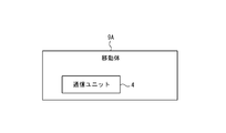
- FIG. 20 is a block diagram of the moving body 9A according to one embodiment.
- a moving body in the present disclosure may include, for example, a vehicle, a ship, an aircraft, and the like.
- the vehicle may include, for example, an automobile, an industrial vehicle, a railway vehicle, a living vehicle, and a fixed-wing aircraft that runs on a runway.
- Vehicles may include, for example, passenger cars, trucks, buses, motorcycles, trolleybuses, and the like.
- Industrial vehicles may include, for example, industrial vehicles for agriculture and construction.
- Industrial vehicles may include, for example, forklifts and golf carts and the like.
- Industrial vehicles for agriculture may include, for example, tractors, tillers, transplanters, binders, combines, and lawn mowers.
- Industrial vehicles for construction may include, for example, bulldozers, scrapers, excavators, mobile cranes, dump trucks, and road rollers. Vehicles may include those that are manually driven.
- the classification of vehicles is not limited to the example described above.
- an automobile may include an industrial vehicle capable of traveling on a road. The same vehicle may be included in multiple classifications.
- the ship may include, for example, a marine jet, a boat, a tanker, and the like.
- Aircraft may include, for example, fixed-wing aircraft, rotary-wing aircraft, and the like.
- the mobile unit 9A includes the communication unit 4.
- the mobile unit 9A may include arbitrary components in order to perform the desired function of the mobile unit 9A, for example.
- the moving body 9A when the moving body 9A is an automobile, the moving body 9A may include an engine, a brake, a steering wheel, and the like.
- FIG. 21 is a block diagram of the base station 9B according to one embodiment.
- Base station in the present disclosure indicates a fixed base or the like capable of wireless communication with the mobile unit 9A.
- the “base station” in the present disclosure may include wireless equipment managed by a telecommunications carrier, a wireless operator, or the like.
- the base station 9B includes the communication unit 4.
- the base station 9B may include at least the array antenna 1 and the controller 6B connected to the array antenna 1 among the components of the communication unit 4 shown in FIG.
- the base station 9B may include arbitrary components in order to perform the desired function of the base station 9B, for example.
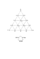
- the antenna elements 100 shown in FIG. 5 may be arranged in a triangular lattice pattern in the array antenna 1A.
- FIG. 22 shows an example in which the antenna elements 100 are arranged in a triangular lattice shape.
- the position P1 shown in FIG. 22 indicates the position of the antenna element 100.
- the sixth direction shown in FIG. 22 is a direction that forms an angle of less than 90 degrees with the fourth direction.
- the seventh direction is a direction intersecting with the fourth direction and the sixth direction.
- the antenna element 100A shown in FIG. 1, the antenna element 100B shown in FIG. 12, the antenna element 100C shown in FIG. 14 and the antenna element 100D shown in FIG. 17 may be arranged in a triangular lattice shape.
- descriptions such as “first”, “second”, and “third” are examples of identifiers for distinguishing the configuration.
- the configurations distinguished by the description such as “first” and “second” in the present disclosure can exchange the numbers in the configurations.
- the first frequency can exchange the identifiers “first” and “second” for the second frequency.
- the exchange of identifiers is done simultaneously. Even after exchanging the identifiers, the configurations are distinguished.
- the identifier may be deleted.
- the configuration in which the identifier is deleted is distinguished by the code.
Landscapes
- Details Of Aerials (AREA)
- Aerials With Secondary Devices (AREA)
- Support Of Aerials (AREA)
- Variable-Direction Aerials And Aerial Arrays (AREA)
Abstract
La présente invention concerne un élément d'antenne amélioré, une antenne réseau, une unité de communication, un corps mobile et une station de base. Un élément d'antenne selon la présente invention comprend : une partie conductrice; un conducteur de masse; un premier nombre prédéterminé de conducteurs de connexion, ledit premier nombre prédéterminé étant supérieur ou égal à 3; une première ligne d'alimentation électrique; une seconde ligne d'alimentation électrique; et un filtre. La partie conductrice s'étend le long d'un premier plan et comprend une pluralité de premiers conducteurs. Le conducteur de masse est positionné à une certaine distance de la partie conductrice et s'étire le long du premier plan. Les conducteurs de connexion s'étendent du conducteur de masse en direction de la partie conductrice. La première ligne d'alimentation électrique est configurée de manière à être connectée électromagnétiquement à la partie conductrice La seconde ligne d'alimentation électrique est configurée de manière à être connectée électromagnétiquement à la partie conductrice au niveau d'une position qui est différente de la position dans laquelle la première ligne d'alimentation électrique est connectée. Le filtre est configuré de façon à être électriquement connecté à la première ligne d'alimentation électrique et/ou la seconde ligne d'alimentation électrique. Le filtre est superposé sur le conducteur de masse.
Priority Applications (3)
| Application Number | Priority Date | Filing Date | Title |
|---|---|---|---|
| EP19879975.1A EP3876348A4 (fr) | 2018-11-02 | 2019-10-24 | Élément d'antenne, antenne réseau, unité de communication, corps mobile et station de base |
| US17/290,769 US11843174B2 (en) | 2018-11-02 | 2019-10-24 | Antenna element, array antenna, communication unit, mobile body, and base station |
| CN201980069229.1A CN112930623B (zh) | 2018-11-02 | 2019-10-24 | 天线元件、阵列天线、通信单元、移动体以及基站 |
Applications Claiming Priority (2)
| Application Number | Priority Date | Filing Date | Title |
|---|---|---|---|
| JP2018207430A JP7064428B2 (ja) | 2018-11-02 | 2018-11-02 | アンテナ素子、アレイアンテナ、通信ユニット、移動体及び基地局 |
| JP2018-207430 | 2018-11-02 |
Publications (1)
| Publication Number | Publication Date |
|---|---|
| WO2020090630A1 true WO2020090630A1 (fr) | 2020-05-07 |
Family
ID=70464442
Family Applications (1)
| Application Number | Title | Priority Date | Filing Date |
|---|---|---|---|
| PCT/JP2019/041788 Ceased WO2020090630A1 (fr) | 2018-11-02 | 2019-10-24 | Élément d'antenne, antenne réseau, unité de communication, corps mobile et station de base |
Country Status (5)
| Country | Link |
|---|---|
| US (1) | US11843174B2 (fr) |
| EP (1) | EP3876348A4 (fr) |
| JP (1) | JP7064428B2 (fr) |
| CN (1) | CN112930623B (fr) |
| WO (1) | WO2020090630A1 (fr) |
Cited By (1)
| Publication number | Priority date | Publication date | Assignee | Title |
|---|---|---|---|---|
| JPWO2023149479A1 (fr) * | 2022-02-03 | 2023-08-10 |
Families Citing this family (4)
| Publication number | Priority date | Publication date | Assignee | Title |
|---|---|---|---|---|
| WO2020262384A1 (fr) * | 2019-06-25 | 2020-12-30 | 京セラ株式会社 | Antenne, module de communication sans fil et dispositif de communication sans fil |
| JP6926174B2 (ja) * | 2019-11-26 | 2021-08-25 | 京セラ株式会社 | アンテナ、無線通信モジュール及び無線通信機器 |
| WO2021252059A1 (fr) * | 2020-06-11 | 2021-12-16 | Commscope Technologies Llc | Ensemble déphaseur pour éléments rayonnants dipôles à base de polymère |
| EP4583647A4 (fr) | 2022-10-07 | 2026-04-22 | Samsung Electronics Co Ltd | Structure de connexion utilisant un élément élastique et dispositif électronique la comprenant |
Citations (7)
| Publication number | Priority date | Publication date | Assignee | Title |
|---|---|---|---|---|
| JP2004514364A (ja) * | 2000-11-14 | 2004-05-13 | エイチアールエル ラボラトリーズ,エルエルシー | 多重周波数帯域における電磁インピーダンスの大きいテクスチャ化表面 |
| JP2005094360A (ja) * | 2003-09-17 | 2005-04-07 | Kyocera Corp | アンテナ装置および無線通信装置 |
| JP2007037109A (ja) * | 2004-09-30 | 2007-02-08 | Toto Ltd | マイクロストリップアンテナ |
| JP2009535942A (ja) * | 2006-04-27 | 2009-10-01 | レイスパン コーポレーション | メタマテリアル構造に基づくアンテナ、デバイス、及びシステム |
| JP2011109414A (ja) * | 2009-11-17 | 2011-06-02 | Toshiba Tec Corp | 周期構造体 |
| US20170125895A1 (en) * | 2014-08-13 | 2017-05-04 | International Business Machines Corporation | Wireless communications package with integrated antennas and air cavity |
| JP2018074583A (ja) * | 2016-10-28 | 2018-05-10 | サムソン エレクトロ−メカニックス カンパニーリミテッド. | アンテナ及びこれを備えるアンテナモジュール |
Family Cites Families (11)
| Publication number | Priority date | Publication date | Assignee | Title |
|---|---|---|---|---|
| JPH06350322A (ja) * | 1993-06-02 | 1994-12-22 | Uniden Corp | 複数送受アンテナ給電装置 |
| JP3863464B2 (ja) * | 2002-07-05 | 2006-12-27 | 株式会社ヨコオ | フィルタ内蔵アンテナ |
| JP4009230B2 (ja) * | 2003-05-28 | 2007-11-14 | 京セラ株式会社 | 円偏波アレーアンテナおよびそれを用いたアンテナ付き基板 |
| CN1875520A (zh) | 2003-10-30 | 2006-12-06 | 松下电器产业株式会社 | 天线装置 |
| JP4557169B2 (ja) | 2005-10-03 | 2010-10-06 | 株式会社デンソー | アンテナ |
| WO2010116675A1 (fr) * | 2009-03-30 | 2010-10-14 | 日本電気株式会社 | Antenne de résonateur |
| CN102576940B (zh) * | 2010-03-12 | 2016-05-04 | 株式会社村田制作所 | 无线通信器件及金属制物品 |
| JP5408166B2 (ja) * | 2011-03-23 | 2014-02-05 | 株式会社村田製作所 | アンテナ装置 |
| JP2013197986A (ja) * | 2012-03-21 | 2013-09-30 | Panasonic Corp | アンテナ装置 |
| JP2017011369A (ja) * | 2015-06-17 | 2017-01-12 | キヤノン株式会社 | 構造体及びアンテナ |
| JP6658705B2 (ja) * | 2017-09-20 | 2020-03-04 | Tdk株式会社 | アンテナモジュール |
-
2018
- 2018-11-02 JP JP2018207430A patent/JP7064428B2/ja active Active
-
2019
- 2019-10-24 EP EP19879975.1A patent/EP3876348A4/fr not_active Withdrawn
- 2019-10-24 WO PCT/JP2019/041788 patent/WO2020090630A1/fr not_active Ceased
- 2019-10-24 US US17/290,769 patent/US11843174B2/en active Active
- 2019-10-24 CN CN201980069229.1A patent/CN112930623B/zh not_active Expired - Fee Related
Patent Citations (7)
| Publication number | Priority date | Publication date | Assignee | Title |
|---|---|---|---|---|
| JP2004514364A (ja) * | 2000-11-14 | 2004-05-13 | エイチアールエル ラボラトリーズ,エルエルシー | 多重周波数帯域における電磁インピーダンスの大きいテクスチャ化表面 |
| JP2005094360A (ja) * | 2003-09-17 | 2005-04-07 | Kyocera Corp | アンテナ装置および無線通信装置 |
| JP2007037109A (ja) * | 2004-09-30 | 2007-02-08 | Toto Ltd | マイクロストリップアンテナ |
| JP2009535942A (ja) * | 2006-04-27 | 2009-10-01 | レイスパン コーポレーション | メタマテリアル構造に基づくアンテナ、デバイス、及びシステム |
| JP2011109414A (ja) * | 2009-11-17 | 2011-06-02 | Toshiba Tec Corp | 周期構造体 |
| US20170125895A1 (en) * | 2014-08-13 | 2017-05-04 | International Business Machines Corporation | Wireless communications package with integrated antennas and air cavity |
| JP2018074583A (ja) * | 2016-10-28 | 2018-05-10 | サムソン エレクトロ−メカニックス カンパニーリミテッド. | アンテナ及びこれを備えるアンテナモジュール |
Non-Patent Citations (4)
| Title |
|---|
| L. JIANG ET AL.: "A CMOS UWB On-Chip Antenna With a MIM Capacitor Loading AMC", IEEE TRANS. ELECTRON DEVICES, vol. 59, no. 6, 2012, pages 1757 - 1764, XP011444194, DOI: 10.1109/TED.2012.2191589 * |
| MURAKAMI ET AL.: "Low-attitude design and band characteristic of artificial magnetic conductor using dielectric substrate", IEICE ACADEMIC JOURNAL (B, vol. J98-B, no. 2, pages 172 - 179 |
| MURAKAMI ET AL.: "Optimum configuration of reflector for dipole antenna with AMC reflector", IEICE ACADEMIC JOURNAL (B, vol. J98-B, no. 11, pages 1212 - 1220 |
| See also references of EP3876348A4 |
Cited By (2)
| Publication number | Priority date | Publication date | Assignee | Title |
|---|---|---|---|---|
| JPWO2023149479A1 (fr) * | 2022-02-03 | 2023-08-10 | ||
| JP7660723B2 (ja) | 2022-02-03 | 2025-04-11 | 京セラ株式会社 | アンテナ素子およびアレイアンテナ |
Also Published As
| Publication number | Publication date |
|---|---|
| US20210376489A1 (en) | 2021-12-02 |
| JP2020072452A (ja) | 2020-05-07 |
| CN112930623A (zh) | 2021-06-08 |
| EP3876348A1 (fr) | 2021-09-08 |
| JP7064428B2 (ja) | 2022-05-10 |
| EP3876348A4 (fr) | 2022-07-27 |
| US11843174B2 (en) | 2023-12-12 |
| CN112930623B (zh) | 2024-03-12 |
Similar Documents
| Publication | Publication Date | Title |
|---|---|---|
| WO2020090630A1 (fr) | Élément d'antenne, antenne réseau, unité de communication, corps mobile et station de base | |
| US11387572B2 (en) | Antenna element, array antenna, communication unit, mobile object, and base station | |
| CN111630714B (zh) | 天线、无线通信设备、车轮、轮胎气压监视系统以及车辆 | |
| US11831076B2 (en) | Antenna, wireless communication module, and wireless communication device | |
| US11916294B2 (en) | Antenna, wireless communication module, and wireless communication device | |
| US11764479B2 (en) | Antenna, bicycle, display apparatus, and unmanned aircraft | |
| US11955736B2 (en) | Antenna, wireless communication module, and wireless communication device | |
| WO2020090837A1 (fr) | Antenne, antenne réseau, module de communication radio et équipement de communication radio | |
| US12074385B2 (en) | Antenna, wireless communication module, and wireless communication device | |
| US11784402B2 (en) | Antenna, wireless communication module, and wireless communication device | |
| US12160055B2 (en) | Antenna, wireless communication module, and wireless communication device | |
| JP7137012B2 (ja) | アンテナ、無線通信モジュール及び無線通信機器 |
Legal Events
| Date | Code | Title | Description |
|---|---|---|---|
| 121 | Ep: the epo has been informed by wipo that ep was designated in this application |
Ref document number: 19879975 Country of ref document: EP Kind code of ref document: A1 |
|
| NENP | Non-entry into the national phase |
Ref country code: DE |
|
| ENP | Entry into the national phase |
Ref document number: 2019879975 Country of ref document: EP Effective date: 20210602 |