WO2020095924A1 - Corps assemblé de substrat de matériau piézoélectrique et substrat de support, son procédé de fabrication et élément d'onde acoustique - Google Patents
Corps assemblé de substrat de matériau piézoélectrique et substrat de support, son procédé de fabrication et élément d'onde acoustique Download PDFInfo
- Publication number
- WO2020095924A1 WO2020095924A1 PCT/JP2019/043392 JP2019043392W WO2020095924A1 WO 2020095924 A1 WO2020095924 A1 WO 2020095924A1 JP 2019043392 W JP2019043392 W JP 2019043392W WO 2020095924 A1 WO2020095924 A1 WO 2020095924A1
- Authority
- WO
- WIPO (PCT)
- Prior art keywords
- piezoelectric material
- substrate
- silicon
- material substrate
- silicon oxide
- Prior art date
- Legal status (The legal status is an assumption and is not a legal conclusion. Google has not performed a legal analysis and makes no representation as to the accuracy of the status listed.)
- Ceased
Links
Images



Classifications
-
- H—ELECTRICITY
- H03—ELECTRONIC CIRCUITRY
- H03H—IMPEDANCE NETWORKS, e.g. RESONANT CIRCUITS; RESONATORS
- H03H9/00—Networks comprising electromechanical or electro-acoustic elements; Electromechanical resonators
- H03H9/02—Details
- H03H9/02535—Details of surface acoustic wave devices
- H03H9/02543—Characteristics of substrate, e.g. cutting angles
- H03H9/02574—Characteristics of substrate, e.g. cutting angles of combined substrates, multilayered substrates, piezoelectrical layers on not-piezoelectrical substrate
-
- H—ELECTRICITY
- H03—ELECTRONIC CIRCUITRY
- H03H—IMPEDANCE NETWORKS, e.g. RESONANT CIRCUITS; RESONATORS
- H03H3/00—Apparatus or processes specially adapted for the manufacture of impedance networks, resonating circuits, resonators
- H03H3/007—Apparatus or processes specially adapted for the manufacture of impedance networks, resonating circuits, resonators for the manufacture of electromechanical resonators or networks
- H03H3/08—Apparatus or processes specially adapted for the manufacture of impedance networks, resonating circuits, resonators for the manufacture of electromechanical resonators or networks for the manufacture of resonators or networks using surface acoustic waves
-
- H—ELECTRICITY
- H03—ELECTRONIC CIRCUITRY
- H03H—IMPEDANCE NETWORKS, e.g. RESONANT CIRCUITS; RESONATORS
- H03H9/00—Networks comprising electromechanical or electro-acoustic elements; Electromechanical resonators
- H03H9/02—Details
- H03H9/02535—Details of surface acoustic wave devices
- H03H9/02543—Characteristics of substrate, e.g. cutting angles
- H03H9/02559—Characteristics of substrate, e.g. cutting angles of lithium niobate or lithium-tantalate substrates
-
- H—ELECTRICITY
- H03—ELECTRONIC CIRCUITRY
- H03H—IMPEDANCE NETWORKS, e.g. RESONANT CIRCUITS; RESONATORS
- H03H9/00—Networks comprising electromechanical or electro-acoustic elements; Electromechanical resonators
- H03H9/25—Constructional features of resonators using surface acoustic waves
-
- H—ELECTRICITY
- H10—SEMICONDUCTOR DEVICES; ELECTRIC SOLID-STATE DEVICES NOT OTHERWISE PROVIDED FOR
- H10N—ELECTRIC SOLID-STATE DEVICES NOT OTHERWISE PROVIDED FOR
- H10N30/00—Piezoelectric or electrostrictive devices
- H10N30/01—Manufacture or treatment
- H10N30/07—Forming of piezoelectric or electrostrictive parts or bodies on an electrical element or another base
- H10N30/072—Forming of piezoelectric or electrostrictive parts or bodies on an electrical element or another base by laminating or bonding of piezoelectric or electrostrictive bodies
-
- H—ELECTRICITY
- H10—SEMICONDUCTOR DEVICES; ELECTRIC SOLID-STATE DEVICES NOT OTHERWISE PROVIDED FOR
- H10N—ELECTRIC SOLID-STATE DEVICES NOT OTHERWISE PROVIDED FOR
- H10N30/00—Piezoelectric or electrostrictive devices
- H10N30/01—Manufacture or treatment
- H10N30/07—Forming of piezoelectric or electrostrictive parts or bodies on an electrical element or another base
- H10N30/072—Forming of piezoelectric or electrostrictive parts or bodies on an electrical element or another base by laminating or bonding of piezoelectric or electrostrictive bodies
- H10N30/073—Forming of piezoelectric or electrostrictive parts or bodies on an electrical element or another base by laminating or bonding of piezoelectric or electrostrictive bodies by fusion of metals or by adhesives
-
- H—ELECTRICITY
- H10—SEMICONDUCTOR DEVICES; ELECTRIC SOLID-STATE DEVICES NOT OTHERWISE PROVIDED FOR
- H10N—ELECTRIC SOLID-STATE DEVICES NOT OTHERWISE PROVIDED FOR
- H10N30/00—Piezoelectric or electrostrictive devices
- H10N30/80—Constructional details
- H10N30/85—Piezoelectric or electrostrictive active materials
- H10N30/853—Ceramic compositions
Definitions
- the present invention relates to a bonded body of a piezoelectric material substrate and a support substrate, a manufacturing method thereof, and an acoustic wave device.
- SOI substrates are widely used to realize higher speed and lower power consumption of CMOS devices.
- the high frequency characteristics of the CMOS device are deteriorated due to the fixed charges of SiO 2 .
- SiO 2 the fixed charges of SiO 2 .
- the effective resistivity decreases, the electric field leaks, and the parasitic capacitance occurs.
- Non-Patent Document 2 a trap level is formed by forming a polycrystalline silicon layer. Further, it has been reported that by reducing the crystallite size of the polycrystalline silicon layer, the level density is improved and the suppression effect is enhanced (Non-Patent Document 3).
- Non-Patent Document 4 a high-performance acoustic wave filter using a bonded substrate made of a piezoelectric body, a SiO 2 film and a silicon substrate has been realized (Non-Patent Document 4).
- a high-performance acoustic wave filter using a bonded substrate made of a piezoelectric body, a SiO 2 film and a silicon substrate has been realized (Non-Patent Document 4).
- deterioration of characteristics due to fixed charges of the SiO 2 film is predicted, as in the CMOS device.
- Patent Document 1 discloses a structure for forming an amorphous Si film or a polycrystalline Si film on the surface of a silicon substrate as a method of suppressing the problem.
- the amorphous Si film and the polycrystalline Si film are formed by the CVD method at a temperature of 400 to 1000 ° C. Therefore, a large film stress remains after the film formation. It has been found that the bonded substrate composed of the piezoelectric body, the SiO 2 film and the silicon substrate has a large difference in thermal expansion coefficient, so that the bonded body frequently breaks in the process involving heating, which is a problem. It has been found that the problem of cracks and cracks becomes more serious when the film stress is inherent.
- An object of the present invention is to bond a piezoelectric material substrate and a silicon substrate via a bonding layer made of silicon oxide, while preventing damage and cracks in the bonded body, and at the same time, to provide an effective resistance of the bonded body in a wide frequency range. It is to improve the rate.
- the manufacturing method of the joined body according to the present invention A silicon film forming step of providing a silicon film on a supporting substrate made of silicon by a physical vapor deposition method, A heat treatment step of forming an intermediate layer by heat-treating the silicon film at a temperature of 400 ° C. or more and 600 ° C. or less, and a piezoelectric material substrate on the supporting substrate via a bonding layer made of silicon oxide and the intermediate layer. It is characterized by having a joining step of joining to each other.
- the joined body according to the present invention A support substrate made of silicon, Piezoelectric material substrate, An intermediate layer provided by heat-treating a silicon film provided on the support substrate by a physical vapor deposition method at a temperature of 400 ° C. or more and 600 ° C. or less, and provided between the intermediate layer and the piezoelectric material substrate.
- An electrode is provided on the bonded body and the piezoelectric material substrate.
- the present inventor when joining a piezoelectric material substrate and a silicon substrate via a joining layer made of silicon oxide, provides a silicon film on a supporting substrate made of silicon by a sputtering method, and makes this film made of silicon oxide. Attempts were made to bond to the piezoelectric material substrate via the bonding layer. Since the physical vapor deposition method is a low temperature process, unlike the case where a polycrystalline silicon film or an amorphous silicon film is provided as in the manufacturing method described in the prior art document, the residual stress in the silicon film is small, and as a result, It was thought that cracks and breaks could be suppressed.
- the present inventor tried to form a silicon film on a silicon substrate by physical vapor deposition, and then heat-treat this silicon film at a temperature of 400 ° C. or more and 600 ° C. or less.
- the heat-treated silicon film was bonded to the piezoelectric material substrate via the bonding layer made of silicon oxide, it was found that cracks or cracks were unlikely to occur in the bonded body.
- the effective resistivity was kept high over a wide temperature range, and the present invention was reached.
- the present inventor observed the microstructure of a silicon film formed on a silicon substrate by physical vapor deposition before and after the heat treatment with a microscope. However, no clear difference in the microstructure could be found before and after the heat treatment. On the other hand, when the silicon film is heat-treated, the effective resistivity of the bonded body is kept high over a wide temperature range, so that the microstructure of the silicon film or the microstructure at the interface between the silicon film and the silicon substrate is not changed. It is clear that this is happening. However, at this time, the method of clarifying this microstructural change by physical means is unknown, and it is considered that it is difficult and impractical to clarify such a change.
- (A) shows the supporting substrate 1, (b) shows a state where the silicon film 2 is formed on the supporting substrate 1, and (c) shows a state where the silicon film 2 is heat-treated to form the intermediate layer 3. And (d) shows a state in which the first silicon oxide layer 4 is provided on the intermediate layer 3.
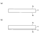
- (A) shows the piezoelectric material substrate 5, and (b) shows a state in which the second silicon oxide layer 6 is provided on the piezoelectric material substrate 5.
- (A) shows a state where the first silicon oxide layer 4 and the second silicon oxide layer 6 are in contact with each other, and (b) shows a bonded body 8.
- (A) shows a state in which the piezoelectric material substrate 5A of the bonded body 8A is thinned, and (b) shows the acoustic wave element 9.
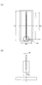
- (A) shows the CPW type electrode used in the examples, and (b) shows an enlarged view of the Vb portion of (a).
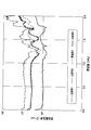
- 7 is a graph showing changes in effective resistivity with respect to frequency for elements of Examples and Comparative Examples.
- a support substrate 1 having a pair of main surfaces 1a and 1b is prepared.
- the support substrate 1 is made of silicon.
- a silicon film 2 is formed on the main surface 1a of the support substrate 1 by a physical vapor deposition method.
- the silicon film 2 and the supporting substrate 1 are heat-treated at a temperature of 400 ° C. or higher and 600 ° C. or lower to provide the intermediate layer 3 made of silicon (FIG. 1C).
- the first silicon oxide layer 4 can be provided on the intermediate layer 3 (FIG. 1D).
- a piezoelectric material substrate 5 having a pair of main surfaces 5a and 5b is prepared.
- a second bonding layer 6 made of silicon oxide is provided on the main surface 5b of the piezoelectric material substrate 5.
- the surface of the first silicon oxide layer 4 and the surface of the second silicon oxide layer 6 are respectively surface-activated by irradiating plasma to form an activated bonding surface.
- the activation surface of the first silicon oxide layer 4 on the support substrate 1 and the activation surface of the second silicon oxide layer 6 on the piezoelectric material substrate 5 are separated. Contact and bond directly.
- the bonded body 8 can be obtained as shown in FIG.
- the first silicon oxide layer 4 and the second silicon oxide layer 6 are usually integrated to form an integrated bonding layer 7.
- electrodes may be provided on the piezoelectric material substrate 5.
- the main surface 5a of the piezoelectric material substrate 5 is processed to make the substrate 5 thin, and a thinned piezoelectric material substrate 5A is obtained.
- 5c is a processed surface.
- a predetermined electrode 10 is formed on the processed surface 5c of the piezoelectric material substrate 5A of the bonded body 8A, and the acoustic wave element 9 can be obtained.
- a silicon film is provided on a supporting substrate made of silicon by a physical vapor deposition method.
- the type of silicon forming the support substrate is not particularly limited, but single crystal silicon is preferable, and silicon may be doped with phosphorus or boron.
- the silicon constituting the support substrate is preferably high resistance silicon having a volume resistivity of 1000 ⁇ ⁇ cm or more.
- the silicon film is formed on the supporting substrate by physical vapor deposition.
- physical vapor deposition is preferably performed at a temperature of 200 ° C. or lower, more preferably 150 ° C. or lower, and particularly preferably 100 ° C. or lower.
- the physical vapor deposition method includes a sputtering method and a vacuum vapor deposition method.
- the sputtering method the reactive sputtering method is preferable from the viewpoint of stability of film quality and film formation rate.
- a target made of metallic Si is sputtered with Ar ions and then reacted with oxygen plasma to form a silicon oxide film.
- a vacuum vapor deposition method using ion beam assist is preferable in order to improve film density and surface smoothness.
- the temperature rise during film formation can be suppressed to 150 ° C or lower.
- the intermediate layer is formed by heat-treating the silicon film at a temperature of 400 ° C. or higher and 600 ° C. or lower. This not only prevents cracks and cracks in the bonded body, but also improves the effective resistivity of the bonded body over a wide frequency range.
- the thickness of the intermediate layer is preferably 50 nm or more, and particularly preferably 100 nm or more.
- the thickness of the intermediate layer is preferably 2 ⁇ m or less, more preferably 1 ⁇ m or less.
- the time for heat treatment is preferably 2 to 10 hours, and the atmosphere for heat treatment is preferably an atmosphere of an inert gas such as nitrogen or argon, or a vacuum environment.
- the piezoelectric material substrate is bonded to the supporting substrate via the bonding layer made of silicon oxide and the intermediate layer.
- a silicon oxide layer can be provided on the intermediate layer, and this silicon oxide layer can be directly bonded to the piezoelectric material substrate.
- the first silicon oxide layer is provided on the intermediate layer on the supporting substrate, the second silicon oxide layer is provided on the piezoelectric material substrate, and the first silicon oxide layer and the second silicon oxide layer are provided.
- the bonding layer can be generated by directly bonding.
- the method for forming this silicon oxide layer is not limited, but sputtering, chemical vapor deposition (CVD), and vapor deposition can be exemplified.
- the silicon oxide layer can be formed by sputtering oxygen into the intermediate layer, ion implantation, or heating in an oxidizing atmosphere.
- the thickness of the bonding layer made of silicon oxide is preferably 0.05 ⁇ m or more, more preferably 0.1 ⁇ m or more, and particularly preferably 0.2 ⁇ m or more.
- the thickness of the bonding layer is preferably 3 ⁇ m or less, preferably 2.5 ⁇ m or less, and more preferably 2.0 ⁇ m or less.
- the piezoelectric material substrate is preferably lithium tantalate (LT) single crystal, lithium niobate (LN) single crystal, or lithium niobate-lithium tantalate solid solution. These are suitable as surface acoustic wave devices for high frequencies and wideband frequencies because they have a high propagation speed of elastic waves and a large electromechanical coupling coefficient.
- each main surface 5a, 5b of the piezoelectric material substrate 5 is not particularly limited.
- the X axis that is the propagation direction of the surface acoustic wave is It is preferable to use the one rotated in the direction of 32 to 55 ° from the Y axis to the Z axis at the center and (180 °, 58 to 35 °, 180 °) in Euler angle display because the propagation loss is small.
- the piezoelectric material substrate is made of lithium niobate
- the size of the piezoelectric material substrate is not particularly limited, but for example, the diameter is 100 to 200 mm and the thickness is 0.15 to 1 ⁇ m.
- the silicon layer Before directly bonding the surface of the piezoelectric material substrate and the silicon oxide layer on the intermediate layer or directly bonding the first silicon oxide layer and the second silicon oxide layer, It is preferable to irradiate the silicon layer with oxygen plasma at 150 ° C. or lower to activate each surface.
- the pressure during such surface activation is preferably 100 Pa or less, more preferably 80 Pa or less. Further, the atmosphere may be only oxygen, but nitrogen gas may be contained in addition to oxygen.
- the temperature during oxygen plasma irradiation is set to 150 ° C. or lower. This makes it possible to obtain a bonded body having high bonding strength and without deterioration of the piezoelectric material. From this viewpoint, the temperature during oxygen plasma irradiation is set to 150 ° C. or lower, It is more preferable that the temperature is 100 ° C. or lower.
- the energy when irradiating the surface of the piezoelectric material substrate with oxygen plasma is preferably 100 to 150 W.
- the product of energy and irradiation time during oxygen plasma irradiation is preferably 20 to 50 Wh. Further, the irradiation time of oxygen plasma is preferably 30 minutes or more.
- the pressure during plasma irradiation on the surface of the silicon oxide layer is preferably 100 Pa or lower, more preferably 80 Pa or lower.
- the energy at this time is preferably 30 to 120 W.
- the product of energy and irradiation time during plasma irradiation is preferably 1 Wh or less.
- the surface of the piezoelectric material substrate and the surface of each silicon oxide layer are flattened before the plasma treatment.
- Methods for flattening each surface include lap polishing and chemical mechanical polishing (CMP).
- the arithmetic average roughness Ra of the flat surface is preferably 1.0 nm or less, more preferably 0.3 nm or less.
- the first silicon oxide layer and the second silicon oxide layer are brought into contact with each other, or the silicon oxide layer and the piezoelectric material substrate are brought into contact with each other to directly bond them. After that, it is preferable to improve the bonding strength by performing an annealing treatment.
- the temperature during the annealing treatment is preferably 100 ° C. or higher and 300 ° C. or lower.
- the joined body of the present invention can be suitably used for acoustic wave devices.
- Known surface acoustic wave devices include surface acoustic wave devices, Lamb wave devices, thin film resonators (FBARs), and the like.
- FBARs thin film resonators
- a surface acoustic wave device has an IDT (Interdigital Transducer) electrode (also called a comb-shaped electrode or a comb-shaped electrode) on the input side for exciting surface acoustic waves and an output side for receiving surface acoustic waves on the surface of a piezoelectric material substrate.
- IDT electrode Interdigital Transducer
- the material forming the electrodes (electrode pattern) on the piezoelectric material substrate is preferably aluminum, aluminum alloy, copper or gold, and more preferably aluminum or aluminum alloy.
- the aluminum alloy it is preferable to use Al mixed with 0.3 to 5% by weight of Cu.
- Ti, Mg, Ni, Mo, or Ta may be used instead of Cu.
- Example 1 As described with reference to FIGS. 1 to 4, bonded bodies according to examples of the present invention were obtained. Specifically, a high resistance ( ⁇ 2 k ⁇ ⁇ cm) Si substrate (supporting substrate) 1 having a thickness of 0.23 mm and a diameter of 150 mm was prepared. This supporting substrate 1 was introduced into a sputtering device (“RAS-1100BII” manufactured by Syncron Corporation), and a silicon film 2 having a thickness of about 500 nm was formed. The film forming conditions at this time are as follows. Bias power: 6000W Ar gas flow rate: 100sccm Microwave power: 1500W Rate: 0.3nm / sec Chamber pressure during film formation: 0.1Pa
- the support substrate 1 on which the silicon film 2 was formed was taken out of the chamber and heat-treated in a clean oven at a temperature of 500 ° C. for 10 hours to form the intermediate layer 3.
- the atmosphere during the heat treatment is a nitrogen atmosphere, and the atmosphere pressure is 1 atm.
- the support substrate 1 after the heat treatment was again introduced into the sputtering apparatus, and then the first silicon oxide layer 4 made of SiO 2 was formed to a thickness of 600 nm.
- a piezoelectric material substrate 5 made of a 42 ° Y-cut black lithium tantalate substrate having a mirror surface of 0.25 mm in thickness was introduced into the same chamber to form a second silicon oxide layer 6.
- the film forming conditions at this time are as follows. However, when forming a silicon film by sputtering, O 2 gas was introduced at a flow rate of 200 sccm in order to oxidize the silicon.
- Bias power 6000W Ar gas flow rate: 100sccm
- Microwave power 1500W Rate: 0.3nm / sec Chamber pressure during film formation: 0.1Pa
- the support substrate 1 and the piezoelectric material substrate 5 after film formation were taken out from the chamber, and the first silicon oxide layer 4 and the second silicon oxide layer 6 were each subjected to CMP (chemical mechanical polishing) over a thickness of about 100 nm. Ra of each surface after this was about 0.2 nm, and a very smooth smooth surface was obtained.
- CMP chemical mechanical polishing
- each surface of the first silicon oxide layer 4 and the second silicon oxide layer 6 was cleaned, and particles were removed from each surface.
- the cleaned first and second silicon oxide layers were brought into contact with each other as shown in FIG. In order to obtain sufficient bonding strength, it was kept in an oven at 120 ° C for 10 hours.
- the piezoelectric material substrate of the bonded body 8 taken out from the oven was ground and polished to finally reduce the thickness to 1 ⁇ m.
- FIGS. 5A and 5B For the purpose of evaluating the high frequency characteristics of the bonded body 8A manufactured in this way, a coplanar waveguide (CPW) having a configuration as shown in FIGS. 5A and 5B was manufactured on a piezoelectric material substrate.
- FIG. 5A shows a planar pattern of CPW
- FIG. 5B shows the shape of the CPW end portion of FIG. 5A.
- the design specifications of CPW are shown below.
- L3 3100 ⁇ m W1: 60 ⁇ m W2: 3000 ⁇ m
- FIG. 6 shows the frequency change of the effective resistivity (Example 1).
- Example 1 Comparative Example 1
- the silicon oxide layer 4 was formed on the supporting substrate without forming the intermediate layer 3 that functions as a trap rich layer. Others were the same as in Example 1 to obtain a joined body. With respect to this joined body, the frequency change of the effective resistivity was measured in the same manner as in Example 1, and the results are shown in FIG.
- Example 1 As compared with Comparative Example 1 having no trap rich layer, the effective resistivity was significantly higher over the entire frequency range. For example, at 1 GHz, the effective resistivity in Comparative Example 1 was 1 ⁇ 10 4 ⁇ ⁇ cm, but in Example 1, it was 3 ⁇ 10 4 ⁇ ⁇ cm, and the effective resistivity was tripled. That is, in Example 1, it was confirmed that the characteristics were improved particularly in the high frequency region.
- Example 2 a bonded body was prepared in the same manner as in Example 1, except that the silicon layer 2 formed by the sputtering method was not heat-treated. With respect to this joined body, the frequency change of the effective resistivity was measured in the same manner as in Example 1, and the results are shown in FIG.
- Example 1 As compared with Comparative Example 2, the effective resistivity was significantly higher over the entire frequency range.
- the effective resistivity in Comparative Example 2 is 2 ⁇ 10 4 ⁇ ⁇ cm, but in Example 1, it is 3 ⁇ 10 4 ⁇ ⁇ cm, and the effective resistivity is 1.5 times higher. It was This means that the silicon layer formed on the silicon substrate by sputtering changes its properties by heat treatment and improves the effective resistivity.
- Example 3 A bonded body was prepared in the same manner as in Example 1. However, the silicon film 2 was not formed on the supporting substrate by the sputtering method. Instead, polycrystalline silicon was deposited on the support substrate at 700 ° C. to a thickness of 500 nm by the LP-CVD method. With respect to this joined body, the frequency change of the effective resistivity was measured in the same manner as in Example 1, and the results are shown in FIG.
- Example 1 and Comparative Examples 1, 2, and 3 were placed in a clean oven at a temperature of 250 ° C., and each joined body was taken out after 20 hours. As a result, the bonded bodies of Example 1 and Comparative Examples 1 and 2 were free from cracks and cracks, and the effect of suppressing residual stress by low temperature film formation was confirmed. On the other hand, the joined body of Comparative Example 3 was split into two.
Landscapes
- Physics & Mathematics (AREA)
- Acoustics & Sound (AREA)
- Engineering & Computer Science (AREA)
- Manufacturing & Machinery (AREA)
- Chemical & Material Sciences (AREA)
- Materials Engineering (AREA)
- Ceramic Engineering (AREA)
- Surface Acoustic Wave Elements And Circuit Networks Thereof (AREA)
- Crystals, And After-Treatments Of Crystals (AREA)
- Physical Vapour Deposition (AREA)
- Piezo-Electric Transducers For Audible Bands (AREA)
- Piezo-Electric Or Mechanical Vibrators, Or Delay Or Filter Circuits (AREA)
Abstract
Priority Applications (6)
| Application Number | Priority Date | Filing Date | Title |
|---|---|---|---|
| CN201980005268.5A CN112913139A (zh) | 2018-11-09 | 2019-11-06 | 压电性材料基板与支撑基板的接合体、其制造方法以及弹性波元件 |
| EP19882081.3A EP3713085A4 (fr) | 2018-11-09 | 2019-11-06 | Corps assemblé de substrat de matériau piézoélectrique et substrat de support, son procédé de fabrication et élément d'onde acoustique |
| JP2020511833A JPWO2020095924A1 (ja) | 2018-11-09 | 2019-11-06 | 圧電性材料基板と支持基板との接合体、その製造方法および弾性波素子 |
| KR1020207014752A KR102413294B1 (ko) | 2018-11-09 | 2019-11-06 | 압전성 재료 기판과 지지 기판의 접합체, 그 제조 방법 및 탄성파 소자 |
| US16/898,925 US12101079B2 (en) | 2018-11-09 | 2020-06-11 | Method of producing a bonded body of piezoelectric material substrate |
| JP2023042726A JP7503167B2 (ja) | 2018-11-09 | 2023-03-17 | 圧電性材料基板と支持基板との接合体、その製造方法および弾性波素子 |
Applications Claiming Priority (2)
| Application Number | Priority Date | Filing Date | Title |
|---|---|---|---|
| JP2018211338 | 2018-11-09 | ||
| JP2018-211338 | 2018-11-09 |
Related Child Applications (1)
| Application Number | Title | Priority Date | Filing Date |
|---|---|---|---|
| US16/898,925 Continuation US12101079B2 (en) | 2018-11-09 | 2020-06-11 | Method of producing a bonded body of piezoelectric material substrate |
Publications (1)
| Publication Number | Publication Date |
|---|---|
| WO2020095924A1 true WO2020095924A1 (fr) | 2020-05-14 |
Family
ID=70612025
Family Applications (1)
| Application Number | Title | Priority Date | Filing Date |
|---|---|---|---|
| PCT/JP2019/043392 Ceased WO2020095924A1 (fr) | 2018-11-09 | 2019-11-06 | Corps assemblé de substrat de matériau piézoélectrique et substrat de support, son procédé de fabrication et élément d'onde acoustique |
Country Status (7)
| Country | Link |
|---|---|
| US (1) | US12101079B2 (fr) |
| EP (1) | EP3713085A4 (fr) |
| JP (2) | JPWO2020095924A1 (fr) |
| KR (1) | KR102413294B1 (fr) |
| CN (1) | CN112913139A (fr) |
| TW (1) | TWI815970B (fr) |
| WO (1) | WO2020095924A1 (fr) |
Cited By (6)
| Publication number | Priority date | Publication date | Assignee | Title |
|---|---|---|---|---|
| JPWO2022168498A1 (fr) * | 2021-02-05 | 2022-08-11 | ||
| JPWO2022201627A1 (fr) * | 2021-03-25 | 2022-09-29 | ||
| WO2024004333A1 (fr) * | 2022-06-27 | 2024-01-04 | 日本碍子株式会社 | Substrat composite et procédé de production de substrat composite |
| US12239022B2 (en) * | 2018-01-22 | 2025-02-25 | Ngk Insulators, Ltd. | Assembly of piezoelectric material substrate and supporting substrate |
| WO2026048449A1 (fr) * | 2024-08-30 | 2026-03-05 | グローバルウェーハズ・ジャパン株式会社 | Procédé de fabrication de substrat composite, substrat composite et dispositif à ondes acoustiques |
| WO2026074869A1 (fr) * | 2024-10-04 | 2026-04-09 | 日本碍子株式会社 | Substrat composite, son procédé de fabrication et élément à ondes acoustiques de surface |
Families Citing this family (7)
| Publication number | Priority date | Publication date | Assignee | Title |
|---|---|---|---|---|
| TWI815970B (zh) * | 2018-11-09 | 2023-09-21 | 日商日本碍子股份有限公司 | 壓電性材料基板與支持基板的接合體、及其製造方法 |
| CN112420914B (zh) * | 2020-11-23 | 2022-09-16 | 济南晶正电子科技有限公司 | 一种复合薄膜、制备方法及电子元器件 |
| KR102741639B1 (ko) | 2021-11-19 | 2024-12-16 | (주)위드멤스 | 기판 접합체 및 기판 접합 방법 |
| TW202544875A (zh) * | 2023-11-09 | 2025-11-16 | 日商日本碍子股份有限公司 | 接合體、元件及接合體之製造方法 |
| US12566343B2 (en) * | 2023-11-10 | 2026-03-03 | HyperLight Corporation | Thin film lithium-containing photonics wafer having a trap-rich substrate |
| WO2026074868A1 (fr) * | 2024-10-04 | 2026-04-09 | 日本碍子株式会社 | Substrat composite, son procédé de fabrication et élément à ondes acoustiques de surface |
| CN119997789A (zh) * | 2025-02-08 | 2025-05-13 | 达波科技(上海)有限公司 | 一种复合压电衬底及其制备方法与应用 |
Citations (5)
| Publication number | Priority date | Publication date | Assignee | Title |
|---|---|---|---|---|
| JP2011061269A (ja) * | 2009-09-07 | 2011-03-24 | Seiko Epson Corp | 弾性表面波デバイスの製造方法 |
| US20170063332A1 (en) | 2015-08-25 | 2017-03-02 | Avago Technologies General Ip (Singapore) Pte. Ltd. | Surface acoustic wave (saw) resonator having trap-rich region |
| WO2017163722A1 (fr) * | 2016-03-25 | 2017-09-28 | 日本碍子株式会社 | Procédé de liage |
| WO2018016169A1 (fr) * | 2016-07-20 | 2018-01-25 | 信越化学工業株式会社 | Procédé de fabrication d'un substrat composite de dispositif à ondes acoustiques de surface |
| WO2018180827A1 (fr) * | 2017-03-31 | 2018-10-04 | 日本碍子株式会社 | Corps lié et élément à ondes acoustiques |
Family Cites Families (15)
| Publication number | Priority date | Publication date | Assignee | Title |
|---|---|---|---|---|
| JP2001260099A (ja) * | 2000-03-22 | 2001-09-25 | Shimadzu Corp | 高抵抗シリコン膜の製造方法及び微細加工構造体 |
| CN102002673B (zh) * | 2010-09-17 | 2011-10-26 | 陕西师范大学 | 纳米晶硅-氧化铝/氧化硅热电薄膜材料的制备方法 |
| CN110554561B (zh) * | 2013-01-15 | 2023-03-21 | Hoya株式会社 | 掩膜板坯料、相移掩膜板及半导体器件的制造方法 |
| JP5934424B2 (ja) * | 2013-02-19 | 2016-06-15 | 日本碍子株式会社 | 弾性波デバイスの製法 |
| FR3037443B1 (fr) * | 2015-06-12 | 2018-07-13 | Soitec | Heterostructure et methode de fabrication |
| US10381998B2 (en) * | 2015-07-28 | 2019-08-13 | Qorvo Us, Inc. | Methods for fabrication of bonded wafers and surface acoustic wave devices using same |
| FR3049763B1 (fr) * | 2016-03-31 | 2018-03-16 | Soitec | Substrat semi-conducteur sur isolant pour applications rf |
| JP6250856B1 (ja) | 2016-07-20 | 2017-12-20 | 信越化学工業株式会社 | 表面弾性波デバイス用複合基板及びその製造方法とこの複合基板を用いた表面弾性波デバイス |
| JP2018058738A (ja) * | 2016-10-07 | 2018-04-12 | 旭硝子株式会社 | 表示装置用カバーガラスおよび電子機器 |
| CN109891747B (zh) | 2016-11-11 | 2023-07-14 | 信越化学工业株式会社 | 复合基板、表面弹性波器件及复合基板的制造方法 |
| JP2018125325A (ja) * | 2017-01-30 | 2018-08-09 | パナソニック・タワージャズセミコンダクター株式会社 | 半導体装置及びその製造方法 |
| TWI780103B (zh) * | 2017-05-02 | 2022-10-11 | 日商日本碍子股份有限公司 | 彈性波元件及其製造方法 |
| TWI787475B (zh) * | 2018-03-29 | 2022-12-21 | 日商日本碍子股份有限公司 | 接合體及彈性波元件 |
| CN112074622B (zh) * | 2018-05-16 | 2021-07-27 | 日本碍子株式会社 | 压电性材料基板与支撑基板的接合体 |
| TWI815970B (zh) * | 2018-11-09 | 2023-09-21 | 日商日本碍子股份有限公司 | 壓電性材料基板與支持基板的接合體、及其製造方法 |
-
2019
- 2019-09-23 TW TW108134168A patent/TWI815970B/zh active
- 2019-11-06 CN CN201980005268.5A patent/CN112913139A/zh active Pending
- 2019-11-06 JP JP2020511833A patent/JPWO2020095924A1/ja active Pending
- 2019-11-06 KR KR1020207014752A patent/KR102413294B1/ko active Active
- 2019-11-06 EP EP19882081.3A patent/EP3713085A4/fr active Pending
- 2019-11-06 WO PCT/JP2019/043392 patent/WO2020095924A1/fr not_active Ceased
-
2020
- 2020-06-11 US US16/898,925 patent/US12101079B2/en active Active
-
2023
- 2023-03-17 JP JP2023042726A patent/JP7503167B2/ja active Active
Patent Citations (5)
| Publication number | Priority date | Publication date | Assignee | Title |
|---|---|---|---|---|
| JP2011061269A (ja) * | 2009-09-07 | 2011-03-24 | Seiko Epson Corp | 弾性表面波デバイスの製造方法 |
| US20170063332A1 (en) | 2015-08-25 | 2017-03-02 | Avago Technologies General Ip (Singapore) Pte. Ltd. | Surface acoustic wave (saw) resonator having trap-rich region |
| WO2017163722A1 (fr) * | 2016-03-25 | 2017-09-28 | 日本碍子株式会社 | Procédé de liage |
| WO2018016169A1 (fr) * | 2016-07-20 | 2018-01-25 | 信越化学工業株式会社 | Procédé de fabrication d'un substrat composite de dispositif à ondes acoustiques de surface |
| WO2018180827A1 (fr) * | 2017-03-31 | 2018-10-04 | 日本碍子株式会社 | Corps lié et élément à ondes acoustiques |
Non-Patent Citations (4)
| Title |
|---|
| "A Nanocrystalline Silicon Surface-Passivation Layer on an HR-Si Substrate for RFICs", IEEE ELECTRON DEVICE LETTERS, vol. 32, no. 3, March 2011 (2011-03-01), pages 369 - 371 |
| "Impact of Si substrate resistivity on the non-linear behavior of RF CPW transmission lines", PROCEEDINGS OF THE 3RD EUROPEAN MICROWAVE INTEGRATED CIRCUITS CONFERENCE, pages 36 - 39 |
| "Low-Loss CPW Lines on surface Stabilized High-Resistivity Silicon", IEEE MICROWAVE AND GUIDED WAVE LETTERS, vol. 9, no. 10, October 1999 (1999-10-01), pages 395 - 397 |
| I. H. P. SAW TECHNOLOGY AND ITS APPLICATION TO MICROACOUSTIC COMPOUNDS (INVITED), PROCEEDINGS OF IUS, 2017 |
Cited By (9)
| Publication number | Priority date | Publication date | Assignee | Title |
|---|---|---|---|---|
| US12239022B2 (en) * | 2018-01-22 | 2025-02-25 | Ngk Insulators, Ltd. | Assembly of piezoelectric material substrate and supporting substrate |
| JPWO2022168498A1 (fr) * | 2021-02-05 | 2022-08-11 | ||
| JP7612721B2 (ja) | 2021-02-05 | 2025-01-14 | 日本碍子株式会社 | 複合基板、弾性表面波素子および複合基板の製造方法 |
| JPWO2022201627A1 (fr) * | 2021-03-25 | 2022-09-29 | ||
| JP7526260B2 (ja) | 2021-03-25 | 2024-07-31 | 日本碍子株式会社 | 接合体およびその製造方法 |
| WO2024004333A1 (fr) * | 2022-06-27 | 2024-01-04 | 日本碍子株式会社 | Substrat composite et procédé de production de substrat composite |
| JPWO2024004333A1 (fr) * | 2022-06-27 | 2024-01-04 | ||
| WO2026048449A1 (fr) * | 2024-08-30 | 2026-03-05 | グローバルウェーハズ・ジャパン株式会社 | Procédé de fabrication de substrat composite, substrat composite et dispositif à ondes acoustiques |
| WO2026074869A1 (fr) * | 2024-10-04 | 2026-04-09 | 日本碍子株式会社 | Substrat composite, son procédé de fabrication et élément à ondes acoustiques de surface |
Also Published As
| Publication number | Publication date |
|---|---|
| EP3713085A1 (fr) | 2020-09-23 |
| KR20200078571A (ko) | 2020-07-01 |
| JP2023080110A (ja) | 2023-06-08 |
| TW202038489A (zh) | 2020-10-16 |
| JP7503167B2 (ja) | 2024-06-19 |
| TWI815970B (zh) | 2023-09-21 |
| JPWO2020095924A1 (ja) | 2021-02-15 |
| US20200304095A1 (en) | 2020-09-24 |
| EP3713085A4 (fr) | 2021-01-13 |
| KR102413294B1 (ko) | 2022-06-27 |
| US12101079B2 (en) | 2024-09-24 |
| CN112913139A (zh) | 2021-06-04 |
Similar Documents
| Publication | Publication Date | Title |
|---|---|---|
| JP7503167B2 (ja) | 圧電性材料基板と支持基板との接合体、その製造方法および弾性波素子 | |
| CN111066243B (zh) | 弹性波元件及其制造方法 | |
| KR102287003B1 (ko) | 접합체 및 탄성파 소자 | |
| JP6648346B1 (ja) | 圧電性材料基板と支持基板との接合体 | |
| KR102867683B1 (ko) | 표면 탄성파 디바이스용 복합 기판 및 그 제조 방법 | |
| JP6648339B2 (ja) | 圧電性材料基板と支持基板との接合体およびその製造方法 | |
| JP6621561B1 (ja) | 圧電性材料基板と支持基板との接合体および弾性波素子 | |
| CN110574290A (zh) | 弹性波元件及其制造方法 | |
| JP6648338B2 (ja) | 圧電性材料基板と支持基板との接合体およびその製造方法 | |
| WO2024004333A1 (fr) | Substrat composite et procédé de production de substrat composite | |
| KR102961427B1 (ko) | 복합 기판 및 복합 기판의 제조 방법 | |
| JP7526260B2 (ja) | 接合体およびその製造方法 | |
| JP6621574B1 (ja) | 接合体および弾性波素子 | |
| EP4068625A1 (fr) | Corps assemblé d'un substrat de matériau piézoélectrique et d'un substrat de support |
Legal Events
| Date | Code | Title | Description |
|---|---|---|---|
| ENP | Entry into the national phase |
Ref document number: 2020511833 Country of ref document: JP Kind code of ref document: A |
|
| ENP | Entry into the national phase |
Ref document number: 20207014752 Country of ref document: KR Kind code of ref document: A |
|
| 121 | Ep: the epo has been informed by wipo that ep was designated in this application |
Ref document number: 19882081 Country of ref document: EP Kind code of ref document: A1 |
|
| ENP | Entry into the national phase |
Ref document number: 2019882081 Country of ref document: EP Effective date: 20200618 |
|
| NENP | Non-entry into the national phase |
Ref country code: DE |