WO2020095959A1 - Substrat à film réfléchissant multicouche, ébauche de masque réfléchissant, procédé de production de masque réfléchissant, et procédé de production de dispositif semi-conducteur - Google Patents
Substrat à film réfléchissant multicouche, ébauche de masque réfléchissant, procédé de production de masque réfléchissant, et procédé de production de dispositif semi-conducteur Download PDFInfo
- Publication number
- WO2020095959A1 WO2020095959A1 PCT/JP2019/043546 JP2019043546W WO2020095959A1 WO 2020095959 A1 WO2020095959 A1 WO 2020095959A1 JP 2019043546 W JP2019043546 W JP 2019043546W WO 2020095959 A1 WO2020095959 A1 WO 2020095959A1
- Authority
- WO
- WIPO (PCT)
- Prior art keywords
- film
- defect
- substrate
- coordinates
- coordinate
- Prior art date
- Legal status (The legal status is an assumption and is not a legal conclusion. Google has not performed a legal analysis and makes no representation as to the accuracy of the status listed.)
- Ceased
Links
Images


Classifications
-
- G—PHYSICS
- G01—MEASURING; TESTING
- G01N—INVESTIGATING OR ANALYSING MATERIALS BY DETERMINING THEIR CHEMICAL OR PHYSICAL PROPERTIES
- G01N21/00—Investigating or analysing materials by the use of optical means, i.e. using sub-millimetre waves, infrared, visible or ultraviolet light
- G01N21/84—Systems specially adapted for particular applications
- G01N21/88—Investigating the presence of flaws or contamination
- G01N21/95—Investigating the presence of flaws or contamination characterised by the material or shape of the object to be examined
- G01N21/956—Inspecting patterns on the surface of objects
-
- G—PHYSICS
- G03—PHOTOGRAPHY; CINEMATOGRAPHY; ANALOGOUS TECHNIQUES USING WAVES OTHER THAN OPTICAL WAVES; ELECTROGRAPHY; HOLOGRAPHY
- G03F—PHOTOMECHANICAL PRODUCTION OF TEXTURED OR PATTERNED SURFACES, e.g. FOR PRINTING, FOR PROCESSING OF SEMICONDUCTOR DEVICES; MATERIALS THEREFOR; ORIGINALS THEREFOR; APPARATUS SPECIALLY ADAPTED THEREFOR
- G03F1/00—Originals for photomechanical production of textured or patterned surfaces, e.g., masks, photo-masks, reticles; Mask blanks or pellicles therefor; Containers specially adapted therefor; Preparation thereof
- G03F1/22—Masks or mask blanks for imaging by radiation of 100nm or shorter wavelength, e.g. X-ray masks, extreme ultraviolet [EUV] masks; Preparation thereof
- G03F1/24—Reflection masks; Preparation thereof
-
- G—PHYSICS
- G03—PHOTOGRAPHY; CINEMATOGRAPHY; ANALOGOUS TECHNIQUES USING WAVES OTHER THAN OPTICAL WAVES; ELECTROGRAPHY; HOLOGRAPHY
- G03F—PHOTOMECHANICAL PRODUCTION OF TEXTURED OR PATTERNED SURFACES, e.g. FOR PRINTING, FOR PROCESSING OF SEMICONDUCTOR DEVICES; MATERIALS THEREFOR; ORIGINALS THEREFOR; APPARATUS SPECIALLY ADAPTED THEREFOR
- G03F1/00—Originals for photomechanical production of textured or patterned surfaces, e.g., masks, photo-masks, reticles; Mask blanks or pellicles therefor; Containers specially adapted therefor; Preparation thereof
- G03F1/68—Preparation processes not covered by groups G03F1/20 - G03F1/50
- G03F1/82—Auxiliary processes, e.g. cleaning or inspecting
- G03F1/84—Inspecting
-
- G—PHYSICS
- G03—PHOTOGRAPHY; CINEMATOGRAPHY; ANALOGOUS TECHNIQUES USING WAVES OTHER THAN OPTICAL WAVES; ELECTROGRAPHY; HOLOGRAPHY
- G03F—PHOTOMECHANICAL PRODUCTION OF TEXTURED OR PATTERNED SURFACES, e.g. FOR PRINTING, FOR PROCESSING OF SEMICONDUCTOR DEVICES; MATERIALS THEREFOR; ORIGINALS THEREFOR; APPARATUS SPECIALLY ADAPTED THEREFOR
- G03F7/00—Photomechanical, e.g. photolithographic, production of textured or patterned surfaces, e.g. printing surfaces; Materials therefor, e.g. comprising photoresists; Apparatus specially adapted therefor
- G03F7/20—Exposure; Apparatus therefor
Definitions
- the present invention relates to a substrate with a multilayer reflective film, a reflective mask blank, a reflective mask manufacturing method, and a semiconductor device manufacturing method.
- EUV lithography which is an exposure technology using extreme ultra violet (hereinafter referred to as EUV) light
- EUV light refers to light in the wavelength band of the soft X-ray region or the vacuum ultraviolet region, specifically, light having a wavelength of about 0.2 to 100 nm.
- a reflective mask has been proposed as a mask used in EUV lithography.
- the reflective mask has a multilayer reflective film that reflects exposure light formed on a substrate such as glass or silicon, and an absorber film pattern that absorbs exposure light is formed on the multilayer reflective film.
- a reflective mask mounted on the exposure machine In an exposure machine that performs pattern transfer, light incident on a reflective mask mounted on the exposure machine is absorbed in a portion having an absorber film pattern and reflected by a multilayer reflective film in a portion having no absorber film pattern. Then, the reflected light image is transferred onto a semiconductor substrate such as a silicon wafer via a reflection optical system.
- One of the problems is a problem regarding defect information of a mask blank substrate used in a lithography process.
- the position of the defect on the board is specified by the distance from the origin using the coordinate system managed by the defect inspection device with the board center as the origin (0, 0). For this reason, the reference of the absolute value coordinates is not clear, the position accuracy is low, and there are variations in detection among devices. Further, even when the pattern forming thin film is patterned while avoiding defects during pattern writing, it is difficult to avoid defects on the order of ⁇ m. For this reason, the pattern transfer direction is changed, or the transfer position is roughly shifted in the mm order to avoid defects.
- defect position information In order to accurately specify the position of the defect on the multilayer reflective film, it is preferable to obtain defect position information by performing a defect inspection after forming the multilayer reflective film. For that purpose, it is preferable to form the reference mark on the multilayer reflective film formed on the substrate.
- Patent Document 1 in order to accurately specify the position of a minute defect having a sphere-equivalent diameter of about 30 nm, a reflective mask blank substrate for EUV lithography having at least a sphere-equivalent diameter of 30 to 100 nm is used. Forming three marks is disclosed.
- the technology that corrects the drawing data so that the absorber film pattern is formed at the location where the defect exists and reduces the defect Proposed.
- a pattern is formed on the resist film formed on the absorber film by using an electron beam drawing machine.
- the electron beam writer also detects the reference mark with the electron beam and draws a pattern based on the corrected / corrected drawing data based on the detected reference point.
- the coordinate system of the defect inspection device for acquiring the defect data of the mask blank is different from the coordinate system of the electron beam writer. Therefore, when performing electron beam drawing using the reference mark and defect data acquired by the defect inspection apparatus, it is necessary to convert the data into the coordinate system of the electron beam drawing machine.
- the present invention is a substrate with a multilayer reflective film and a reflective mask blank capable of improving the conversion accuracy from the coordinate system of a defect inspection device that detects defects on a multilayer reflective film to the coordinate system of other devices. It is an object of the present invention to provide a method for manufacturing a reflective mask and a method for manufacturing a semiconductor device.
- the present inventors have earnestly studied to improve the accuracy of conversion from the coordinate system of the defect inspection device that detects defects on the multilayer reflective film to the coordinate system of other devices. As a result, they found that there is a correlation between the number of reference marks serving as the reference of the defect position and the coordinate conversion accuracy, and completed the present invention.
- a substrate with a multilayer reflective film comprising: a substrate; and a multilayer reflective film formed on the substrate for reflecting EUV light, It is provided with a reference mark serving as a reference for the position of a defect in the substrate with the multilayer reflective film,
- the multilayer reflective film coated substrate wherein the number of the reference marks is the number previously determined by the following procedures (1) to (7).
- (1) Obtain a first defect coordinate of a defect and a first reference mark coordinate of the reference mark in another substrate with a multilayer reflection film having a plurality of reference marks by the defect inspection device having the first coordinate system. To do.
- the coordinate measuring instrument having the second coordinate system acquires the second defect coordinate of the defect and the second reference mark coordinate of the reference mark in the another multilayer reflective film coated substrate.
- a conversion coefficient for converting the coordinates from the first coordinate system to the second coordinate system is calculated based on the first reference mark coordinates and the second reference mark coordinates.
- the first defect coordinates acquired by the defect inspection apparatus in (1) above can be converted into a third coordinate system based on the second coordinate system. Convert to the defect coordinates of.
- a value of 3 ⁇ is obtained for the difference between the second defect coordinates acquired by the coordinate measuring instrument in (2) above and the third defect coordinates converted in (4) above.
- a value of 3 ⁇ is obtained.
- the number of reference marks having a value of 3 ⁇ of less than 50 nm is determined.
- a reflective mask blank comprising: the substrate with a multilayer reflective film according to any one of configurations 1 to 3; and a laminated film formed on the substrate with a multilayer reflective film.
- a reflective mask blank comprising a substrate and a substrate with a multilayer reflective film having a multilayer reflective film formed on the substrate for reflecting EUV light, and a laminated film formed on the substrate with the multilayer reflective film,
- the substrate with a multilayer reflective film is provided with a reference mark serving as a reference for the position of a defect in the substrate with a multilayer reflective film
- the laminated film includes a transfer reference mark to which the reference mark is transferred
- the reflective mask blank is characterized in that the number of the reference marks is the number determined in advance by the following steps (1) to (7).
- (1) Obtain a first defect coordinate of a defect and a first reference mark coordinate of the reference mark in another substrate with a multilayer reflection film having a plurality of reference marks by the defect inspection device having the first coordinate system. To do.
- (2) Second coordinate coordinates of defects in a reflective mask blank having a laminated film formed on another substrate having a multilayer reflective film and a transfer reference mark by a coordinate measuring instrument having a second coordinate system To obtain the second fiducial mark coordinates of.
- a conversion coefficient for converting the coordinates from the first coordinate system to the second coordinate system is calculated based on the first reference mark coordinates and the second reference mark coordinates.
- the first defect coordinates acquired by the defect inspection apparatus in (1) above can be converted into a third coordinate system based on the second coordinate system. Convert to the defect coordinates of. (5) For the difference between the second defect coordinates acquired by the coordinate measuring instrument in (2) above and the third defect coordinates converted in (4) above, a value of 3 ⁇ is obtained. (6) Obtain the correspondence between the number of reference marks and 3 ⁇ . (7) The number of reference marks having a value of 3 ⁇ of less than 50 nm is determined.
- (Configuration 9) A method of manufacturing a reflective mask, comprising the step of forming a laminated film pattern on the laminated film in the reflective mask blank according to Structure 4 or Structure 8.
- Configuration 10 A method for manufacturing a semiconductor device, comprising the step of forming a transfer pattern on a semiconductor substrate using the reflective mask manufactured by the method for manufacturing a reflective mask according to configuration 9.
- substrate with a multilayer reflective film and reflective type which can improve the conversion precision from the coordinate system of the defect inspection apparatus for detecting the defect on a multilayer reflective film to the coordinate system of other apparatuses.
- a mask blank can be provided.
- a method for manufacturing a reflective mask in which defects are reduced by using these substrates with a multilayer reflective film or a reflective mask blank and correcting writing data based on the defect information thereof, and A method for manufacturing a semiconductor device can be provided.
- FIG. 3 is a plan view of a substrate with a multilayer reflective film and an enlarged view of a reference mark. It is a schematic diagram which shows the cross section of a reflective mask blank. It is a schematic diagram which shows the manufacturing method of a reflective mask. 1 shows a pattern transfer device. The location where the FM is formed when the number of FMs is 8 is shown. 9 is a graph showing the value of 3 ⁇ when the number of FMs is 3 to 8. 9 is a graph showing a calculation result of 3 ⁇ when the number N of reference marks is increased to 200. The formation location of the FM when the number of FMs is 16 is shown. The locations where the AM and FM are formed when the number of AMs is 28 and the number of FMs is 4 are shown. The formation location of the FM when the number of FMs is 3 is shown.
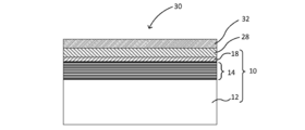
- FIG. 1 is a schematic view showing a cross section of a substrate with a multilayer reflective film according to this embodiment.
- the substrate 10 with a multilayer reflective film includes a substrate 12 and a multilayer reflective film 14 that reflects EUV light that is exposure light.
- the substrate 10 with a multilayer reflective film may include a protective film 18 for protecting the multilayer reflective film 14.
- the multilayer reflective film 14 is formed on the substrate 12, and the protective film 18 is formed on the multilayer reflective film 14.
- the substrate with a multilayer reflective film 10 has four or more reference marks that serve as references for defect positions.
- “on” a substrate or a film includes not only the case where the substrate or the film is in contact with the upper surface but also the case where the substrate or the film is not in contact with the upper surface. That is, “on” the substrate or film includes a case where a new film is formed above the substrate or film, a case where another film is interposed between the substrate and the film, and the like. .. In addition, “upward” does not necessarily mean an upper side in the vertical direction. The term "on top” merely indicates a relative positional relationship between the substrate and the film.
- the substrate 12 used in the substrate 10 with the multilayer reflective film of the present embodiment has a low heat within the range of 0 ⁇ 5 ppb / ° C. in order to prevent distortion of the absorber film pattern due to heat during exposure.
- Those having a coefficient of expansion are preferably used.
- As a material having a low coefficient of thermal expansion in this range for example, SiO 2 —TiO 2 glass, multi-component glass ceramics, etc. can be used.
- the main surface on the side of the substrate 12 where the transfer pattern (the absorber film pattern described later corresponds to this) is preferably processed to enhance the flatness.
- the flatness is preferably 0.1 ⁇ m or less, more preferably 0.05 ⁇ m or less, particularly preferably 0.05 ⁇ m or less in a 132 mm ⁇ 132 mm area of the main surface of the substrate 12 on the side where the transfer pattern is formed. It is preferably 0.03 ⁇ m or less.
- the main surface on the side opposite to the side on which the transfer pattern is formed is a surface fixed to the exposure device by an electrostatic chuck and has a flatness of 1 ⁇ m or less, more preferably 0, in an area of 142 mm ⁇ 142 mm. It is 0.5 ⁇ m or less, particularly preferably 0.03 ⁇ m or less.
- the flatness is a value representing the warp (deformation amount) of the surface indicated by TIR (Total Indicated Reading), and the plane determined by the least squares method with the substrate surface as a reference is the focal plane. It is the absolute value of the height difference between the highest position of the substrate surface above the plane and the lowest position of the substrate surface below the focal plane.
- the surface roughness of the main surface of the substrate 12 on which the transfer pattern is formed is preferably 0.1 nm or less in terms of root mean square roughness (RMS).
- the surface roughness can be measured with an atomic force microscope.
- the substrate 12 preferably has high rigidity in order to prevent the film (such as the multilayer reflective film 14) formed thereon from being deformed due to film stress.
- the substrate 12 preferably has a high Young's modulus of 65 GPa or more.
- the substrate 10 with a multilayer reflective film includes a substrate 12 and a multilayer reflective film 14 formed on the substrate 12.
- the multilayer reflective film 14 is, for example, a multilayer film in which elements having different refractive indexes are periodically stacked.
- the multilayer reflective film 14 has a function of reflecting EUV light.
- the multilayer reflective film 14 includes a thin film of a light element or its compound (high refractive index layer) which is a high refractive index material and a thin film of a heavy element or its compound (low refractive index layer) which is a low refractive index material. ) And are alternately laminated for about 40 to 60 cycles.
- the high refractive index layer and the low refractive index layer may be laminated in this order for a plurality of cycles from the substrate 12 side. In this case, one (high refractive index layer / low refractive index layer) laminated structure has one cycle.
- a plurality of low refractive index layers and a plurality of high refractive index layers may be laminated in this order from the substrate 12 side in this order.
- one (low refractive index layer / high refractive index layer) laminated structure has one cycle.
- the uppermost layer of the multilayer reflective film 14, that is, the surface layer of the multilayer reflective film 14 opposite to the substrate 12 is preferably a high refractive index layer.
- the uppermost layer is the low refractive index layer.
- the low-refractive index layer is the surface of the multi-layer reflective film 14
- the low-refractive index layer is easily oxidized and the reflectivity of the multi-layer reflective film is reduced.
- a high refractive index layer is formed.
- the uppermost layer is the high refractive index layer. In that case, the uppermost high refractive index layer becomes the surface of the multilayer reflective film 14.
- the high refractive index layer may be a layer containing Si.
- the high refractive index layer may include a simple substance of Si or may include a Si compound.
- the Si compound may include Si and at least one element selected from the group consisting of B, C, N, and O.
- the low refractive index material is at least one element selected from the group consisting of Mo, Ru, Rh, and Pt, or at least selected from the group consisting of Mo, Ru, Rh, and Pt. Alloys containing one element can be used.
- a Mo / Si multilayer film in which Mo films and Si films are alternately laminated for about 40 to 60 cycles can be preferably used.
- the multilayer reflective film used in the EUV light region for example, Ru / Si periodic multilayer film, Mo / Be periodic multilayer film, Mo compound / Si compound periodic multilayer film, Si / Nb periodic multilayer film, Si / A Mo / Ru periodic multilayer film, a Si / Mo / Ru / Mo periodic multilayer film, a Si / Ru / Mo / Ru periodic multilayer film, or the like can be used.
- the material of the multilayer reflective film can be selected in consideration of the exposure wavelength.
- the reflectance of such a multilayer reflective film 14 alone is, for example, 65% or more.
- the upper limit of the reflectance of the multilayer reflective film 14 is 73%, for example.
- the thickness and period of the layers included in the multilayer reflective film 14 can be selected so as to satisfy Bragg's law.
- the multilayer reflective film 14 can be formed by a known method.
- the multilayer reflective film 14 can be formed by, for example, an ion beam sputtering method.
- the multilayer reflection film 14 is a Mo / Si multilayer film
- a Mo film having a thickness of about 3 nm is formed on the substrate 12 by using an Mo target by an ion beam sputtering method.
- a Si target is used to form a Si film having a thickness of about 4 nm.
- the multilayer reflective film 14 in which Mo / Si films are laminated for 40 to 60 cycles.
- the surface layer of the multilayer reflective film 14 on the side opposite to the substrate 12 is a layer containing Si (Si film).
- the thickness of the Mo / Si film for one cycle is 7 nm.
- the substrate 10 with a multilayer reflective film of the present embodiment may include a protective film 18 formed on the multilayer reflective film 14.
- the protective film 18 has a function of protecting the multilayer reflective film 14 at the time of patterning or pattern modification of the absorber film described later.
- the protective film 18 is provided, for example, between the multilayer reflective film 14 and the absorber film.
- the material of the protective film 18 examples include Ru, Ru- (Nb, Zr, Y, B, Ti, La, Mo, Co or Re) compounds, Si- (Ru, Rh, Cr or B) compounds, Si, Materials such as Zr, Nb, La and B can be used. Further, a compound in which nitrogen, oxygen, or carbon is added to these can be used. Of these, when a material containing ruthenium (Ru) is applied, the reflectance characteristic of the multilayer reflective film becomes better.
- the material of the protective film 18 is preferably Ru or a Ru- (Nb, Zr, Y, B, Ti, La, Mo, Co or Re) compound.
- the thickness of the protective film 18 is, for example, 1 nm to 5 nm.
- the protective film 18 can be formed by a known method.
- the protective film 18 can be formed by, for example, a magnetron sputtering method or an ion beam sputtering method.
- the substrate 10 with a multilayer reflection film may further have a back surface conductive film on the main surface of the substrate 12 opposite to the side where the multilayer reflection film 14 is formed.
- the back surface conductive film is used when the substrate 10 with a multilayer reflective film or the reflective mask blank is attracted by an electrostatic chuck.
- the substrate 10 with a multilayer reflective film may include a base film formed between the substrate 12 and the multilayer reflective film 14.
- the base film is formed for the purpose of improving the smoothness of the surface of the substrate 12, for example.
- the base film is formed for the purpose of, for example, reducing defects, improving the reflectance of the multilayer reflective film, and correcting the stress of the multilayer reflective film.
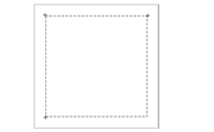
- FIG. 2 is a plan view of the substrate 10 with a multilayer reflective film according to this embodiment.
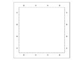
- reference marks 20 are formed in the vicinity of the four corners of the substantially rectangular substrate 10 with a multilayer reflective film.
- the reference mark 20 is a mark used as a reference for the defect position in the defect information.
- FIG. 2 shows an example in which four reference marks 20 are formed, the number of reference marks 20 may be four or more. Further, the four or more reference marks 20 may be arranged on at least two axes.
- an absorber film pattern is formed in a region inside the broken line A (a region of 132 mm ⁇ 132 mm) when a reflective mask is manufactured. In the region outside the broken line A, the absorber film pattern is not formed when the reflective mask is manufactured.
- the reference mark 20 is preferably formed in a region where the absorber film pattern is not formed, that is, in the region above the broken line A or outside the broken line A.
- the reference mark 20 has a substantially cross shape.
- the widths W1 and W2 of the reference mark 20 having a substantially cross shape are, for example, 200 nm or more and 10 ⁇ m or less.
- the length L of the reference mark 20 is, for example, 100 ⁇ m or more and 1500 ⁇ m or less.
- FIG. 2 shows an example of the reference mark 20 having a substantially cross shape, the shape of the reference mark 20 is not limited to this.
- the shape of the reference mark 20 may be, for example, a substantially L shape, a circle, a triangle, a quadrangle, or the like in plan view.
- the cross-sectional shape of the reference mark 20 is, for example, concave.
- concave as used herein means that when the cross section of the substrate 10 with a multilayer reflection film (a cross section perpendicular to the main surface of the substrate 10 with a multilayer reflection film) is viewed, the reference mark 20 faces downward, for example, a step shape or It means that it is formed so as to be concave in a curved shape.
- the depth D of the reference mark 20 formed in a concave shape is preferably 30 nm or more.
- the depth D of the reference mark 20 may be the depth at which the substrate 12 is exposed, but is preferably 100 nm or less, and more preferably 50 nm or less. When the depth D is small, the effect of the present invention can be obtained more significantly.
- the depth D means the distance in the vertical direction from the surface of the substrate with a multilayer reflective film 10 to the deepest position of the bottom of the reference mark 20.
- the method of forming the reference mark 20 is not particularly limited.
- the reference mark 20 can be formed, for example, by laser processing on the surface of the substrate 10 with a multilayer reflective film. At this time, the reference mark 20 may be formed after the multilayer reflective film 14 is formed, and then the protective film 18 may be formed. Alternatively, the multilayer reflective film 14 and the protective film 18 may be formed and then the reference mark 20 is formed. It may be formed.
- the laser processing conditions are as follows, for example.
- Laser power 1 to 120 mW
- Scan speed 0.1-20 mm / s
- Pulse frequency 1 to 100 MHz Pulse width: 3ns to 1000s
- the laser used for laser processing the reference mark 20 may be continuous wave or pulse wave.
- the width W of the reference mark 20 can be made smaller than that of the continuous wave even if the depth D of the reference mark 20 is about the same. Therefore, when the pulse wave is used, it is possible to form the reference mark 20 which has a higher contrast than the continuous wave and is easily detected by the defect inspection device or the electron beam drawing device.
- the method of forming the reference mark 20 is not limited to the laser.
- the reference mark 20 can be formed by, for example, a photolithography method, an FIB (focused ion beam), a processing mark obtained by scanning with a diamond stylus, an indentation by a minute indenter, or an embossing by an imprint method.
- FIB focused ion beam
- the cross-sectional shape of the reference mark 20 is not limited to the concave shape.
- the cross-sectional shape of the reference mark 20 may be a convex shape protruding upward.
- the reference mark 20 has a convex cross-sectional shape, it can be formed by partial film formation by FIB or sputtering.
- the height H of the reference mark 20 formed in a convex shape is preferably 30 nm or more.
- the height H of the reference mark 20 is preferably 100 nm or less, and more preferably 50 nm or less. When the height H is small, the effect of the present invention can be more remarkably obtained.
- the height H means the distance in the vertical direction from the surface of the substrate 10 with the multilayer reflective film to the highest position of the reference mark 20.
- the defect inspection apparatus acquires the reference mark 20 and the coordinates of the defect with high accuracy.
- an absorber film is formed on the protective film 18 of the substrate 10 with the multilayer reflective film.
- a resist film is formed on the absorber film.
- a hard mask film (or an etching mask film) may be formed between the absorber film and the resist film.
- the concave reference mark 20 formed on the substrate 10 with the multilayer reflective film is transferred to the absorber film and the resist film.
- the concave reference mark 20 formed on the substrate 10 with the multilayer reflection film is transferred to the absorber film, the hard mask film and the resist film. ..
- the reference mark 20 formed on the substrate 10 with the multilayer reflective film needs to have a high contrast that can be detected by the defect inspection apparatus.
- a mask substrate / blank defect inspection device "MAGICSM7360" for EUV exposure made by Lasertec which has an inspection light source wavelength of 266 nm
- an EUV made by KLA-Tencor which has an inspection light source wavelength of 193 nm
- a mask / blank defect inspection apparatus “Teron 600 series, for example, Teron 610” or an ABI (Actinic Blank Inspection) apparatus whose inspection light source wavelength is the same as the exposure light source wavelength of 13.5 nm can be used.
- the reference mark 20 transferred to the absorber film and / or the resist film thereon needs to have a high contrast that can be detected by the coordinate measuring device and / or the electron beam drawing device.
- the coordinate measuring device for example, "LAMS-IPRO4" manufactured by KLA-Tencor Co., which measures coordinates with a laser having a wavelength of 365 nm, "PROVE” manufactured by Carl Zeiss Co., which measures coordinates with a laser having a wavelength of 193 nm, and / or A coordinate measuring device mounted on the electron beam drawing apparatus can be used.
- the effect of the present invention can be more remarkably obtained when the coordinate measuring device has a wavelength different from that of the above-described defect inspection device.
- the reference mark 20 can be used as an FM (fiducial mark), for example.
- the FM is a mark used as a reference for defect coordinates when a pattern is drawn by an electron beam drawing apparatus.
- the FM usually has a cross shape as shown in FIG.
- the reference mark 20 By using the reference mark 20 as an FM, defect coordinates can be managed with high accuracy.
- the reference mark 20 transferred to the resist film is used as an FM that is a reference for the defect position.
- the defect coordinates acquired by the defect inspection apparatus can be converted into the coordinate system of the electron beam drawing apparatus by detecting the FM with the electron beam drawing apparatus.
- the drawing data of the pattern drawn by the electron beam drawing apparatus can be corrected so that the defect is arranged under the absorber film pattern. By correcting the writing data, it is possible to reduce the influence of defects on the finally manufactured reflective mask.
- the reference mark 20 can also be used as an AM (alignment mark).
- AM is a mark that can be used as a reference for defect coordinates when inspecting a defect on the substrate 10 with a multilayer reflection film by a defect inspection device.
- AM is not directly used when drawing a pattern by an electron beam drawing apparatus.
- the shape of the AM in plan view is, for example, a circle, a quadrangle, or a cross.
- the FM is formed on the laminated film described later on the substrate 10 with the multilayer reflective film.
- the AM is transferred to the laminated film, but the detection accuracy of the AM can be improved by partially removing the laminated film on the AM.
- AM can be detected by a defect inspection device and a coordinate measuring device.
- the FM can be detected by the coordinate measuring device and the electron beam drawing device. Since both AM and FM can be detected by the coordinate measuring device, their relative positional relationship can be managed with high accuracy. Therefore, it is possible to highly accurately convert the AM-based defect coordinates acquired by the defect inspection apparatus into the FM-based defect coordinates used in the electron beam drawing apparatus.
- the number of AMs is larger than the number of FMs.
- the substrate 10 with a multilayer reflection film of the present embodiment has four or more (for example, N) reference marks 20 (four reference marks in FIG. 2) that serve as references for the positions of defects in the substrate 10 with a multilayer reflection film.
- the value of 3 ⁇ obtained by the following procedures (1) to (5) is less than 50 nm.
- the defect inspection apparatus having the first coordinate system acquires the first defect coordinate of the defect in the substrate 10 with the multilayer reflection film and the first reference mark coordinate of the reference mark 20.
- the coordinate measuring instrument having the second coordinate system acquires the second defect coordinate of the defect and the second reference mark coordinate of the reference mark 20 in the substrate 10 with the multilayer reflection film.
- the defect inspection apparatus obtains the first defect coordinates of the defect in the multilayer reflection film coated substrate 10 and the first reference mark coordinates (x, y) of the N reference marks 20. ..
- the defect inspection device for example, the defect inspection device described above can be used.
- the number of defects for obtaining the value of 3 ⁇ is preferably 3 or more, more preferably 9 or more, and further preferably 15 or more.
- the variation in the size of the N reference marks is small.
- the size of the N reference marks is preferably within ⁇ 5% of their average value, and more preferably within ⁇ 3%.
- the “size” here means, for example, the area of the reference mark in plan view.
- the coordinate measuring instrument acquires the second defect coordinate of the defect in the substrate 10 with the multilayer reflective film and the second reference mark coordinate (u, v) of the N reference marks 20. ..
- the coordinate measuring device for example, the above-mentioned coordinate measuring device can be used.
- the origin can be set at the center of the board.
- the origin may be set at an arbitrary corner of the substrate after acquiring edge coordinates at eight positions (two positions per side) on the four sides of the substrate and performing appropriate tilt correction.
- the coordinates of the reference mark 20 are determined by detecting the edges of the reference mark 20. It can be set at the intersection with the center line of.
- the conversion coefficient for converting the coordinates from the first coordinate system of the defect inspection device to the second coordinate system of the coordinate measuring device is calculated.
- linear conversion affine conversion
- an example of the method of calculating the transform coefficient using the affine transform will be described.
- this function ⁇ is a quadratic function, in order to find a, b, c that minimizes this function, this expression is partially differentiated by a, b, c.
- Partial differentiation is a function that represents the gradient of the error function, so the point where the partially differentiated function is 0 is the minimum value, which is also the minimum value. This can be expressed as follows.
- the conversion coefficient calculated in the above (3) is used to transfer the first defect coordinates acquired by the defect inspection device in the above (1) to the second coordinate system of the coordinate measuring instrument. Convert.
- a value of 3 ⁇ is set for the difference between the second defect coordinate acquired by the coordinate measuring instrument in the above (2) and the third defect coordinate converted in the above (4).
- the difference between the second defect coordinates “actually” acquired by the coordinate measuring device and the third defect coordinate converted into the second coordinate system of the coordinate measuring device using the conversion coefficient is 3 ⁇ .
- Find the value. 3 ⁇ is three times the standard deviation ⁇ . The fact that 3 ⁇ is small means that the conversion accuracy from the first coordinate system of the defect inspection apparatus to the second coordinate system of the coordinate measuring instrument is high.
- the second defect coordinate acquired by the coordinate measuring instrument in (2) above is (s j , t j ), and the third defect coordinate converted into the second coordinate system of the coordinate measuring instrument in (4) above. If the defect coordinates of (S j , T j ) are (S j , T j ), the difference between these coordinates is (s j -S j , t j -T j ). In this case, the value of 3 ⁇ can be obtained by calculating the standard deviation ⁇ of j pieces of data for each of the x-coordinate and the y-coordinate.
- the value of ⁇ can be obtained by the least squares method by applying the result obtained by actually measuring the number of reference marks 20 and measuring 3 ⁇ to the above equation (1).
- the number of reference marks 20 increases, the conversion accuracy of defect coordinates can be improved, and the number of reference marks 20 can be determined based on a desired 3 ⁇ .
- the number of reference marks 20 is preferably 4 or more, and 3 ⁇ can be set to less than 50 nm. Further, the number of reference marks 20 is more preferably 8 or more, and 3 ⁇ can be set to less than 25 nm. The number of reference marks 20 is more preferably 16 or more, and 3 ⁇ can be set to less than 20 nm. Further, from the viewpoint of increasing the number of processes for forming the reference marks 20 and increasing the number of defects when the number of the reference marks 20 is too large, the number of the reference marks 20 is preferably 100 or less. Further, when the number of reference marks 20 exceeds 60, the decrease width of 3 ⁇ tends to be small, and therefore the number of reference marks 20 is more preferably 60 or less.
- the value of 3 ⁇ obtained by the above steps (1) to (5) is less than 50 nm.
- the value of 3 ⁇ is less than 50 nm for both the x-coordinate and y-coordinate data.
- the conversion accuracy from the first coordinate system of the defect inspection apparatus to the second coordinate system of the coordinate measuring device can be improved.
- a user who is provided with the substrate with a multilayer reflective film 10 can collate the defect position specified by the defect inspection device with the drawing data with high accuracy, and in the finally manufactured reflective mask. Defects can be surely reduced.
- the second embodiment uses another substrate with a multilayer reflection film to obtain the correspondence between the number of reference marks and 3 ⁇ , and to provide the multilayer reflection having the number of reference marks determined based on the correspondence. It is different from the first embodiment in that it is a substrate with a film. Other than that, it is the same as the first embodiment. That is, the substrate 10 with a multilayer reflection film of the present embodiment is provided with the reference mark 20 that serves as a reference for the position of a defect in the substrate 10 with a multilayer reflection film, and the number of the reference marks 20 is determined by the following procedure (1 )-(7).
- (1) Obtain a first defect coordinate of a defect and a first reference mark coordinate of the reference mark in another substrate with a multilayer reflection film having a plurality of reference marks by the defect inspection device having the first coordinate system. To do.
- (2) The coordinate measuring instrument having the second coordinate system acquires the second defect coordinate of the defect and the second reference mark coordinate of the reference mark in the another multilayer reflective film coated substrate.
- (3) A conversion coefficient for converting the coordinates from the first coordinate system to the second coordinate system is calculated based on the first reference mark coordinates and the second reference mark coordinates.
- the first defect coordinates acquired by the defect inspection apparatus in (1) above can be converted into a third coordinate system based on the second coordinate system. Convert to the defect coordinates of.
- steps (1) to (5) are the same as the steps (1) to (5) of the first embodiment, except that another substrate with a multilayer reflective film is used.
- Defects in another substrate with a multilayer reflective film may be real defects or programmed defects.
- another substrate with a multilayer reflection film may be one substrate with a multilayer reflection film on which N reference marks are formed.
- the above steps (1) to (6) are performed on one substrate with a multilayer reflection film to obtain the correspondence between the number of reference marks and 3 ⁇ , and the above correspondence is performed in step (7).
- the number of reference marks is determined based on the relationship.
- the other substrate with a multilayer reflective film may be a plurality of substrates with a multilayer reflective film on which 4 to N different reference marks are formed.
- the above steps (1) to (5) are performed for each substrate with a multilayer reflective film, and in step (6), the correspondence between the number of reference marks and 3 ⁇ is acquired, and step (7) At, the number of reference marks is determined based on the correspondence.
- an optimum number of reference marks 20 is provided according to the shape of the reference mark, the defect inspection device and / or the coordinate measuring instrument.
- the substrate 10 with a multilayer reflective film can be obtained.
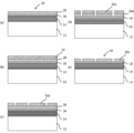
- FIG. 3 is a schematic view showing a cross section of the reflective mask blank 30 of this embodiment.
- the reflective mask blank 30 of the present embodiment can be manufactured by forming the laminated film 28 on the protective film 18 of the substrate 10 with the multilayer reflective film described above.
- the laminated film 28 may be an absorber film that absorbs EUV light.
- the laminated film 28 is an absorber film will be described.
- the absorber film has a function of absorbing EUV light which is exposure light. That is, the difference between the EUV light reflectance of the multilayer reflective film 14 (including the protective film 18 if there is a protective film 18) and the EUV light reflectance of the absorber film is a predetermined value or more. ..
- the reflectance of the absorber film for EUV light is 0.1% or more and 40% or less.
- the absorber film in the reflective mask blank 30 may be called a phase shift film.
- the absorber film preferably has a function of absorbing EUV light and can be removed by etching or the like. It is preferable that the absorber film can be etched by dry etching using a chlorine (Cl) -based gas or a fluorine (F) -based gas.
- the material of the absorber film is not particularly limited as long as the absorber film has such a function.
- the absorber film may have a single layer or a laminated structure.
- a plurality of films made of the same material may be laminated or a plurality of films made of different materials may be laminated.
- the material and composition may change stepwise and / or continuously in the thickness direction of the film.
- the material of the absorber film is preferably tantalum (Ta) alone or a material containing Ta, for example.
- the material containing Ta is, for example, a material containing Ta and B, a material containing Ta and N, a material containing Ta and B and at least one of O and N, a material containing Ta and Si, and Ta and Si.
- the absorber film is composed of, for example, Ni simple substance, Ni-containing material, Cr simple substance, Cr-containing material, Ru simple substance, Ru-containing material, Pd simple substance, Pd-containing material, Mo simple substance, and Mo-containing material. It may include at least one selected from the group.
- the thickness of the absorber film is preferably 30 nm to 100 nm.
- the absorber film can be formed by a known method such as a magnetron sputtering method or an ion beam sputtering method.
- the resist film 32 may be formed on the absorber film (laminated film 28). This aspect is shown in FIG. A resist pattern can be formed by drawing and exposing a pattern on the resist film 32 with an electron beam drawing apparatus and then performing a developing process. By performing dry etching on the absorber film using this resist pattern as a mask, a pattern can be formed on the absorber film.
- the laminated film 28 may include an absorber film and a hard mask film formed on the absorber film.
- the hard mask film is used as a mask when patterning the absorber film.
- the hard mask film and the absorber film are formed of materials having different etching selectivity.
- the material of the absorber film contains tantalum or a tantalum compound
- the material of the hard mask film preferably contains chromium or a chromium compound.
- the chromium compound preferably contains Cr and at least one selected from the group consisting of N, O, C, and H.
- the reflective mask blank 30 of the present embodiment includes four or more (for example, N) reference marks 20 that serve as a reference for the position of a defect on the substrate 10 with a multilayer reflective film.
- the absorber film (laminated film 28) formed on the substrate 10 with the multilayer reflective film may include a transfer reference mark to which the shape of the reference mark 20 is transferred.
- a transfer reference mark to which the shape of the reference mark 20 is transferred.
- the reference mark 20 is concave
- a concave transfer reference mark is formed on the absorber film (laminated film 28) formed thereon.
- a convex transfer reference mark is formed on the absorber film (laminated film 28) formed thereon.
- the reference mark 20 of this embodiment is the same as the reference mark 20 of the first embodiment.
- the transfer reference mark also has a substantially cross shape.
- the widths W1 'and W2' of the transfer reference mark having a substantially cross shape are, for example, 200 nm or more and 10 ⁇ m or less.
- the deviation ⁇ W ( (
- / W1) ⁇ 100) of the width W1 ′ (W2 ′) of the transfer reference mark from the width W1 (W2) of the reference mark 20 may be 10% or less. preferable.
- the deviation ⁇ W is 1% or more, and further the ⁇ W is 3% or more, the effect of the present invention can be more remarkably obtained.
- the length L ′ of the transfer reference mark is, for example, 100 ⁇ m or more and 1500 ⁇ m or less.
- the deviation ⁇ L ( (
- / L) ⁇ 100) of the length L ′ of the transfer reference mark from the length L of the reference mark 20 is preferably 1% or less. Further, when the deviation ⁇ L is 0.05% or more, the effect of the present invention can be more remarkably obtained.
- the transfer reference mark 20 when the reference mark 20 has a substantially circular shape, the transfer reference mark also has a substantially circular shape.
- the deviation (absolute value) of the diameter of the transfer reference mark from the diameter of the reference mark 20 is preferably 10% or less. Further, when the deviation is 1% or more, and further the deviation is 3% or more, the effect of the present invention is more remarkably obtained.
- the transfer reference mark 20 When the reference mark 20 is concave (convex), the transfer reference mark is also concave (convex).
- the depth D '(height H') of the transfer reference mark is preferably 30 nm or more.
- the depth D '(height H') is preferably 100 nm or less, and more preferably 50 nm or less.
- the deviation ⁇ D ( ⁇ H) of the depth D ′ (height H ′) of the transfer reference mark from the depth D (height H) of the reference mark 20 is preferably 10% or less. Further, when the deviation ⁇ D ( ⁇ H) is 0.05% or more, and further when ⁇ D ( ⁇ H) is 1% or more, the effect of the present invention can be more remarkably obtained.
- the value of 3 ⁇ obtained by the following procedures (1) to (5) may be less than 50 nm.
- the defect inspection apparatus having the first coordinate system acquires the first defect coordinate of the defect in the substrate 10 with the multilayer reflection film and the first reference mark coordinate of the reference mark 20.
- the coordinate measuring instrument having the second coordinate system acquires the second defect coordinate of the defect in the reflective mask blank 30 and the second reference mark coordinate of the transfer reference mark.
- the first defect coordinates acquired by the defect inspection apparatus in the above (1) are compared with the second coordinate system of the coordinate measuring machine as a reference. Convert to 3 defect coordinates.
- a value of 3 ⁇ is obtained.
- steps (1) to (5) are the same as the steps (1) to (5) in the substrate 10 with a multilayer reflective film according to the first embodiment described above, but in the step (2), the coordinate measuring device is used. The difference is that the second defect coordinate of the defect in the reflective mask blank 30 and the second reference mark coordinate of the transfer reference mark are acquired.
- the number of reference marks 20 can be determined based on the desired 3 ⁇ .
- the number of reference marks 20 is preferably 4 or more, and 3 ⁇ can be set to less than 50 nm. Further, the number of reference marks 20 is more preferably 8 or more, and 3 ⁇ can be set to less than 25 nm.
- the number of reference marks 20 is more preferably 16 or more, and 3 ⁇ can be set to less than 20 nm.
- the number of the reference marks 20 is preferably 100 or less. Further, when the number of reference marks 20 exceeds 60, the decrease width of 3 ⁇ tends to be small, and therefore the number of reference marks 20 is more preferably 60 or less.
- the value of 3 ⁇ obtained by the above steps (1) to (5) is less than 50 nm.
- the value of 3 ⁇ is less than 50 nm for both the x-coordinate and y-coordinate data.
- the conversion accuracy from the first coordinate system of the defect inspection apparatus to the second coordinate system of the coordinate measuring device can be improved.
- the user who is provided with the reflective mask blank 30 can collate the defect position specified by the defect inspection device with the drawing data with high accuracy, and the defect is produced in the finally manufactured reflective mask. Can be reliably reduced.
- the second fiducial mark coordinates of the transcription fiducial mark transferred to the absorber film (laminated film 28) are acquired in the above procedure (2). Since the FM on the absorber film is used as a reference when a pattern is drawn on the resist film by the electron beam drawing apparatus, by using the second reference mark coordinates of the transfer reference mark transferred to the absorber film, The coordinate conversion accuracy can be further improved. That is, when the absorber film (laminated film 28) is formed on the reference mark, the width and depth of the transfer reference mark transferred to the absorber film are changed, so that the position of the detected reference mark is changed. There are cases.
- the second reference mark coordinates of the transfer reference mark transferred to the absorber film are acquired, and the conversion coefficient is calculated based on the acquired second reference mark coordinates to consider the effect of the reference mark position deviation.
- the converted coefficient can be calculated. As a result, it becomes possible to further improve the coordinate conversion accuracy in the procedure (4).
- the fourth embodiment uses another substrate with a multilayer reflective film and another reflective mask blank having a laminated film on the other substrate with a multilayer reflective film to determine the number of reference marks and 3 ⁇ .
- the reflective mask blank 30 is different from the third embodiment in that the reflective mask blank 30 has the reference marks the number of which is obtained based on the corresponding relationship. Other than that, it is the same as the third embodiment.
- the reflective mask blank 30 of this embodiment includes the reference mark 20 that serves as a reference for the position of a defect in the substrate 10 with a multilayer reflective film.
- the absorber film (laminated film 28) formed on the substrate 10 with the multilayer reflection film includes a transfer reference mark to which the shape of the reference mark 20 is transferred.
- the number of the reference marks 20 is the number obtained in advance by the following procedures (1) to (7). (1) Obtain a first defect coordinate of a defect and a first reference mark coordinate of the reference mark in another substrate with a multilayer reflection film having a plurality of reference marks by the defect inspection device having the first coordinate system. To do.
- a conversion coefficient for converting the coordinates from the first coordinate system to the second coordinate system is calculated based on the first reference mark coordinates and the second reference mark coordinates.
- the first defect coordinates acquired by the defect inspection apparatus in (1) above can be converted into a third coordinate system based on the second coordinate system. Convert to the defect coordinates of.
- the steps (1) to (5) are the same as the steps (1) to (5) of the third embodiment, except that another substrate with a multilayer reflective film and another reflective mask blank are used. is there.
- Another multilayer reflective film coated substrate is the same as that of the third embodiment.
- Another reflective mask blank has a plurality of transfer reference marks to which the reference marks formed on another substrate with a multilayer reflective film are transferred.
- the number of reference marks is obtained using another substrate with a multilayer reflective film and another reflective mask blank, the shape of the reference mark, the shape of the transfer reference mark, the defect inspection device and / or the coordinate measuring instrument. According to the above, it is possible to obtain the substrate 10 with a multilayer reflective film having the optimum number of reference marks 20.
- the reflective mask blank 30 of this embodiment can be used to manufacture the reflective mask 40 of this embodiment.
- a method for manufacturing the reflective mask 40 will be described.
- FIG. 4 is a schematic view showing a method of manufacturing the reflective mask 40.
- a reflective mask blank 30 having the absorber film (laminated film 28) is prepared (FIG. 4A).
- the resist film 32 is formed on the absorber film (FIG. 4B).
- a pattern is drawn on the resist film 32 by an electron beam drawing apparatus, and a development / rinse process is performed to form a resist pattern 32a (FIG. 4C).
- the absorber film (laminated film 28) is dry-etched. As a result, the portion of the absorber film that is not covered with the resist pattern 32a is etched to form the absorber film pattern 28a (FIG. 4D).
- etching gas for example, chlorine-based gas such as Cl 2 , SiCl 4 , CHCl 3 and CCl 4 , a mixed gas containing these chlorine-based gas and O 2 in a predetermined ratio, chlorine-based gas and He are predetermined.
- the resist pattern 32a is removed with, for example, a resist stripping solution.
- the reflective mask 40 of the present embodiment is obtained by performing a wet cleaning process using an acidic or alkaline aqueous solution (FIG. 4E).
- a transfer pattern can be formed on the semiconductor substrate by lithography using the reflective mask 40 of this embodiment. This transfer pattern has a shape obtained by transferring the absorber film pattern 28a of the reflective mask 40.
- a semiconductor device can be manufactured by forming a transfer pattern on the semiconductor substrate using the reflective mask 40.
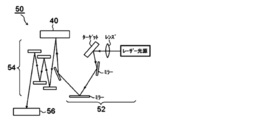
- FIG. 5 shows the pattern transfer device 50.
- the pattern transfer device 50 includes a laser plasma X-ray source 52, a reflective mask 40, and a reduction optical system 54.
- An X-ray reflection mirror is used as the reduction optical system 54.
- the pattern reflected by the reflective mask 40 is normally reduced to about 1/4 by the reduction optical system 54.
- a wavelength band of 13 to 14 nm is used as the exposure wavelength, and it is preset so that the optical path is in vacuum.
- the EUV light generated by the laser plasma X-ray source 52 is made incident on the reflective mask 40.
- the light reflected by the reflective mask 40 is transferred onto the semiconductor substrate 56 with resist via the reduction optical system 54.
- the light incident on the reflective mask 40 is absorbed by the absorber film and is not reflected at the portion where the absorber film pattern 28a is present. On the other hand, the light incident on the portion without the absorber film pattern 28a is reflected by the multilayer reflective film 14.
- the light reflected by the reflective mask 40 enters the reduction optical system 54.
- the light incident on the reduction optical system 54 forms a transfer pattern on the resist layer on the semiconductor substrate 56 with resist.
- a resist pattern can be formed on the semiconductor substrate 56 with resist.
- etching the semiconductor substrate 56 using the resist pattern as a mask for example, a predetermined wiring pattern can be formed on the semiconductor substrate.
- a semiconductor device is manufactured through these steps and other necessary steps.
- the reflective mask blank of this embodiment determines the number of FMs according to, for example, the second embodiment or the fourth embodiment described above.
- a method for manufacturing a reflective mask blank comprising: A step of forming a multilayer reflective film on the substrate to form a substrate with the multilayer reflective film; Forming a number of FMs determined on the basis of a desired 3 ⁇ on the surface of the substrate with a multilayer reflective film; Using the defect inspection apparatus, the first defect coordinates of the defect on the surface of the substrate with the multilayer reflection film and the first FM coordinates of the FM are acquired, and the first FM coordinates are used as a reference. Obtaining a defect map showing the first defect coordinates; A method of manufacturing a reflective mask blank, comprising: forming a laminated film having a transfer FM on which the FM is transferred, on the substrate having the multilayer reflective film.
- the user provided with the reflective mask blank and the defect map can collate the defect position specified by the defect inspection device with the drawing data with high accuracy based on the transfer FM, and finally manufactured. It is possible to reliably reduce defects in the reflective mask.
- the reflective mask blank of the present embodiment determines the number of AMs according to, for example, the second embodiment or the fourth embodiment described above.
- a method for manufacturing a reflective mask blank comprising: A step of forming a multilayer reflective film on the substrate to form a substrate with the multilayer reflective film; Forming a number of AMs determined on the basis of a desired 3 ⁇ on the surface of the substrate with the multilayer reflective film;
- the defect inspection apparatus is used to acquire the first defect coordinates of the defects on the surface of the substrate with the multilayer reflection film and the first AM coordinates of the AM, and thus the first AM coordinates are used as a reference.
- the user provided with the reflective mask blank and the second defect map can collate the defect position specified by the defect inspection apparatus with the drawing data with high accuracy based on FM, and finally, It is possible to surely reduce defects in the manufactured reflective mask.
- Example 1 An SiO 2 —TiO 2 glass substrate (6 inch square, thickness 6.35 mm) was prepared. The end face of this glass substrate was chamfered and ground, and then rough-polished with a polishing liquid containing cerium oxide abrasive grains. The glass substrate after these treatments was set in a carrier of a double-sided polishing machine, and precision polishing was performed under a predetermined polishing condition using an alkaline aqueous solution containing colloidal silica abrasive grains as a polishing liquid. After finishing the precision polishing, the glass substrate was washed.
- the surface roughness of the main surface of the obtained glass substrate was a root mean square roughness (RMS) of 0.10 nm or less.
- the flatness of the main surface of the obtained glass substrate was 30 nm or less in a measurement area of 132 mm ⁇ 132 mm.
- a multilayer reflective film was formed by periodically stacking a Mo film / Si film on the main surface of the glass substrate opposite to the side where the back surface conductive film was formed.
- a Mo target and a Si target were used, and a Mo film and a Si film were alternately laminated on the substrate by ion beam sputtering (using Ar).
- the Mo film has a thickness of 2.8 nm.
- the thickness of the Si film is 4.2 nm.
- the thickness of the Mo / Si film for one cycle is 7.0 nm.
- Such Mo / Si films were laminated for 40 cycles, and finally a Si film was formed to a thickness of 4.0 nm to form a multilayer reflective film.
- a protective film containing a Ru compound was formed on the multilayer reflective film. Specifically, a RuNb target (Ru: 80 atomic%, Nb: 20 atomic%) is used, and a protective film made of a RuNb film is formed on the multilayer reflective film by DC magnetron sputtering in an Ar gas atmosphere. did. The protective film had a thickness of 2.5 nm.
- An FM was formed on the protective film by laser processing.
- the laser processing conditions were as follows.
- Laser type Semiconductor laser with a wavelength of 405 nm
- Laser output 20 mW (continuous wave)
- Spot size 430nm ⁇
- the shape and dimensions of the FM were as follows. Shape: Almost cross-shaped Depth D: 40 nm Width W1, W2: 1 ⁇ m Length L: 1 mm
- the FM formation location was as shown in FIG. 6, and was outside the 132 mm ⁇ 132 mm effective area (area indicated by the broken line).
- the defect inspection device (ABI manufactured by Lasertec Co., Ltd.), the first defect coordinate of the defect in the substrate with the multilayer reflective film and the first FM coordinate of the FM were acquired.
- the number of defects was four.
- An absorber film was formed on the protective film of the substrate with the multilayer reflective film to manufacture a reflective mask blank. Specifically, an absorber film made of a laminated film of TaBN (thickness 56 nm) and TaBO (thickness 14 nm) was formed by DC magnetron sputtering.
- the TaBN film was formed using a TaB target by reactive sputtering in a mixed gas atmosphere of Ar gas and N 2 gas.
- the TaBO film was formed by reactive sputtering in a mixed gas atmosphere of Ar gas and O 2 gas using a TaB target.
- the transfer FM to which the FM was transferred was formed on the laminated film.
- the second defect coordinates of the defects in the reflective mask blank and the second FM coordinates of the transfer FM were acquired.
- a conversion coefficient for converting the coordinates from the first coordinate system of the defect inspection apparatus to the second coordinate system of the coordinate measuring instrument was calculated using the acquired first FM coordinates and second FM coordinates. ..
- the above-mentioned affine transformation formula was used to calculate the transformation coefficient.
- the first defect coordinates acquired by the defect inspection apparatus were converted into the second coordinate system of the coordinate measuring instrument to acquire the third defect coordinates.
- the difference between the third defect coordinate obtained by the conversion and the second defect coordinate obtained by the coordinate measuring instrument was obtained for each of the X coordinate and the Y coordinate.
- Such “difference” absolute value
- ⁇ and 3 ⁇ of this “difference” were calculated.
- 3 ⁇ was 24.2 nm in X coordinate and 23.3 nm in Y coordinate, and both were less than 50 nm.
- a resist film was formed on the absorber film of the reflective mask blank manufactured above.
- a pattern was drawn on the resist film using an electron beam drawing apparatus. When drawing a pattern, four transfer FMs were used as a reference for defect coordinates. After drawing the pattern, a predetermined development process was performed to form a resist pattern on the absorber film.
- a pattern was formed on the absorber film using the resist pattern as a mask. Specifically, the upper TaBO film was dry-etched with a fluorine-based gas (CF 4 gas), and then the lower TaBN film was dry-etched with a chlorine-based gas (Cl 2 gas).
- CF 4 gas fluorine-based gas
- Cl 2 gas chlorine-based gas
- the reflective mask according to Example 1 was obtained by removing the resist pattern remaining on the absorber film pattern with hot sulfuric acid.
- a mask defect inspection apparatus Teon 600 series manufactured by KLA-Tencor
- Example 2 A substrate with a multilayer reflective film and a reflective mask blank were manufactured in the same manner as in Example 1 except that the number of FMs was changed from 8 to 16.
- the FM formation location was as shown in FIG. 9, and was outside the 132 mm ⁇ 132 mm effective area (area indicated by the broken line).
- 3 ⁇ was calculated in the same manner as in Example 1. As a result, in the case of 16 FMs, 3 ⁇ was X coordinate of 18.2 nm and Y coordinate of 18.0 nm, and both were less than 50 nm.
- Example 2 Similar to Example 1, a reflection type mask of Example 2 was obtained by drawing a pattern on a resist film by an electron beam drawing device based on the position information of defects with the transfer FM as a reference.
- a mask defect inspection apparatus Teon 600 series manufactured by KLA-Tencor
- Example 3 A multilayer reflective film-coated substrate of Example 3 using the multilayer reflective film-coated substrate and the reflective mask blank having the eight FMs of Example 1 as another multilayer reflective film-coated substrate and another reflective mask blank. And a reflective mask blank was produced. From the correspondence between the number of FMs obtained in Example 1 and 3 ⁇ , the number of FMs with 3 ⁇ of less than 30 nm was calculated, and the number of FMs was set to 7. In the same manner as in Example 1, the multilayer reflective film and the protective film were formed on the main surface of the glass substrate opposite to the side where the back surface conductive film was formed. FM was formed on the protective film by laser processing, and a substrate with a multilayer reflective film having 7 FMs was manufactured. The shape and dimensions of the FM were as follows. Shape: Almost cross-shaped Depth D: 40 nm Width W1, W2: 1 ⁇ m Length L: 1m
- Example 2 In the same manner as in Example 1, a defect inspection apparatus (ABI, manufactured by Lasertec Co., Ltd.) was used to obtain the first defect coordinates of the defects in the substrate with the multilayer reflective film and the first FM coordinates of the FM, A defect map showing the first defect coordinates with respect to the first FM coordinates was obtained. The number of defects was 5.
- Example 2 In the same manner as in Example 1, a laminated film in which the transfer FM was formed was formed on the protective film, and a reflective mask blank was produced.
- the deviation ⁇ D of the transfer FM depth D ′ from the FM depth D was almost zero.
- the deviations ⁇ W1 and ⁇ W2 of the transfer FM widths W1 ′ and W2 ′ from the FM widths W1 and W2 were 7%, respectively.
- the deviation ⁇ L of the transfer FM length L ′ from the FM length L was 0.1%.
- the second defect coordinates of the defects in the reflective mask blank and the second FM coordinates of the transfer FM were acquired. Similar to the first embodiment, the first defect coordinate is converted into the second coordinate system of the coordinate measuring instrument, and the third defect coordinate obtained by the conversion and the second defect coordinate obtained by the coordinate measuring instrument are converted. The difference from the defect coordinate was obtained for each of the X coordinate and the Y coordinate. As a result, 3 ⁇ was less than 30 nm.
- a reflective mask was manufactured in the same manner as in Example 1.
- a mask defect inspection apparatus Teon 600 series manufactured by KLA-Tencor
- Example 4 Based on the results of FIG. 8 described above, 28 AMs were calculated as the number of AMs having 3 ⁇ of less than 20 nm, and a substrate with a multilayer reflective film and a reflective mask blank of Example 4 were produced. In the same manner as in Example 1, the multilayer reflective film and the protective film were formed on the main surface of the glass substrate opposite to the side where the back surface conductive film was formed.
- AM was formed on the protective film by laser processing.
- the laser processing conditions were as follows.
- Laser type Semiconductor laser with a wavelength of 405 nm
- Laser output 20 mW (continuous wave)
- Spot size 430nm ⁇
- the shape and dimensions of the AM were as follows. Shape: almost circular Depth: 40 nm Diameter: 0.9 ⁇ m
- the AM formation location was as shown in FIG. 10, and was outside the 132 mm ⁇ 132 mm effective area (the area indicated by the broken line).
- the first defect coordinates of the defects in the substrate with the multilayer reflective film and the first AM coordinates of 28 AMs were acquired.
- An absorber film was formed on the protective film of the substrate with the multilayer reflective film to manufacture a reflective mask blank. Specifically, an absorber film made of a laminated film of TaBN (thickness 56 nm) and TaBO (thickness 14 nm) was formed by DC magnetron sputtering.
- the TaBN film was formed using a TaB target by reactive sputtering in a mixed gas atmosphere of Ar gas and N 2 gas.
- the TaBO film was formed by reactive sputtering in a mixed gas atmosphere of Ar gas and O 2 gas using a TaB target.
- 28 transfer AMs to which AMs were transferred were formed.
- the deviation ⁇ D of the transfer AM depth D ′ from the AM depth D was almost zero.
- the deviation of the diameter of the transferred AM from the diameter of the AM was 6%.
- FM was formed on the surface of the absorber film by FIB processing.
- the conditions for FIB processing were as follows. Accelerating voltage: 50kV Beam current value: 20pA
- the shape and dimensions of the FM were as follows. Shape: Almost cross-shaped Depth D: 70 nm Width W1, W2: 5 ⁇ m Length L: 1 mm
- LMS-IPRO4 manufactured by KLA-Tencor
- the first defect coordinates acquired by the defect inspection device were converted into the second coordinate system of the coordinate measuring instrument, and the third defect coordinates were acquired.
- a resist film was formed on the absorber film of the reflective mask blank manufactured above.
- a pattern was drawn on the resist film using an electron beam drawing apparatus.
- FM was used as a reference for defect coordinates.
- the relative positional relationship between the transfer AM and FM was acquired by a coordinate measuring device.
- the position information of the defect with AM as a reference was converted into the position information of the defect with FM as a reference.
- a pattern was drawn on the resist film by an electron beam drawing apparatus based on the position information of the defect based on the FM.
- a pattern was formed on the absorber film using the resist pattern as a mask. Specifically, the upper TaBO film was dry-etched with a fluorine-based gas (CF 4 gas), and then the lower TaBN film was dry-etched with a chlorine-based gas (Cl 2 gas).
- CF 4 gas fluorine-based gas
- Cl 2 gas chlorine-based gas
- the reflective mask according to Example 4 was obtained by removing the resist pattern remaining on the absorber film pattern with hot sulfuric acid.
- a mask defect inspection apparatus Teon 600 series manufactured by KLA-Tencor
- Example 1 A substrate with a multilayer reflective film and a reflective mask blank were manufactured in the same manner as in Example 1 except that the number of FMs was changed from 8 to 3.
- the FM formation location was as shown in FIG. 11, and was outside the 132 mm ⁇ 132 mm effective area (the area indicated by the broken line).
- a reflection type mask of Comparative Example 1 was obtained by drawing a pattern on a resist film by an electron beam drawing apparatus based on the position information of the defect based on the transfer FM.
- the obtained EUV reflective mask was inspected by a mask defect inspection device (Teron 600 series manufactured by KLA-Tencor), the accuracy of coordinate conversion was poor, and therefore the defect could not be hidden under the absorber film pattern. Defects were confirmed in the exposed areas of the multilayer reflective film.
Landscapes
- Physics & Mathematics (AREA)
- General Physics & Mathematics (AREA)
- General Health & Medical Sciences (AREA)
- Chemical & Material Sciences (AREA)
- Analytical Chemistry (AREA)
- Biochemistry (AREA)
- Life Sciences & Earth Sciences (AREA)
- Health & Medical Sciences (AREA)
- Immunology (AREA)
- Pathology (AREA)
- Preparing Plates And Mask In Photomechanical Process (AREA)
- Exposure And Positioning Against Photoresist Photosensitive Materials (AREA)
- Exposure Of Semiconductors, Excluding Electron Or Ion Beam Exposure (AREA)
Abstract
La présente invention permet d'améliorer la précision de conversion à partir d'un système de coordonnées d'un dispositif d'inspection de défaut pour détecter des défauts sur un film réfléchissant multicouche dans un système de coordonnées d'un dispositif autre que le dispositif d'inspection de défaut. Ce substrat à film réfléchissant multicouche comprend des repères de référence dont le nombre est prédéfini par les étapes (1) à (7). À l'étape (1), le dispositif d'inspection de défaut acquiert des premières coordonnées de défaut de défauts et des premières coordonnées de repère de référence de repères de référence sur un substrat à film réfléchissant multicouche différent. À l'étape (2), un dispositif de mesure de coordonnées acquiert des deuxièmes coordonnées de défaut des défauts et des deuxièmes coordonnées de repère de référence des repères de référence sur le substrat à film réfléchissant multicouche différent. À l'étape (3), un coefficient de conversion pour effectuer une conversion de coordonnées à partir d'un système de coordonnées du dispositif d'inspection de défaut dans un système de coordonnées du dispositif de mesure de coordonnées est calculé sur la base des premières coordonnées de repère de référence et des deuxièmes coordonnées de repère de référence. À l'étape (4), les premières coordonnées de défaut sont converties en troisièmes coordonnées de défaut à l'aide du coefficient de conversion calculé à l'étape (3). À l'étape (5), la valeur de 3σ est obtenue pour la différence entre les deuxièmes coordonnées de défaut et les troisièmes coordonnées de défaut. À l'étape (6), la relation de correspondance entre le nombre des repères de référence et 3σ est acquise. À l'étape (7), le nombre des repères de référence auxquels la valeur de 3σ devient inférieure à 50 nm, est déterminé.
Priority Applications (1)
| Application Number | Priority Date | Filing Date | Title |
|---|---|---|---|
| JP2020555553A JP7492456B2 (ja) | 2018-11-07 | 2019-11-06 | 多層反射膜付き基板、反射型マスクブランク、反射型マスクの製造方法、及び半導体装置の製造方法 |
Applications Claiming Priority (2)
| Application Number | Priority Date | Filing Date | Title |
|---|---|---|---|
| JP2018-209973 | 2018-11-07 | ||
| JP2018209973 | 2018-11-07 |
Publications (1)
| Publication Number | Publication Date |
|---|---|
| WO2020095959A1 true WO2020095959A1 (fr) | 2020-05-14 |
Family
ID=70612060
Family Applications (1)
| Application Number | Title | Priority Date | Filing Date |
|---|---|---|---|
| PCT/JP2019/043546 Ceased WO2020095959A1 (fr) | 2018-11-07 | 2019-11-06 | Substrat à film réfléchissant multicouche, ébauche de masque réfléchissant, procédé de production de masque réfléchissant, et procédé de production de dispositif semi-conducteur |
Country Status (3)
| Country | Link |
|---|---|
| JP (1) | JP7492456B2 (fr) |
| TW (1) | TWI829797B (fr) |
| WO (1) | WO2020095959A1 (fr) |
Cited By (4)
| Publication number | Priority date | Publication date | Assignee | Title |
|---|---|---|---|---|
| CN113674250A (zh) * | 2021-08-25 | 2021-11-19 | 长鑫存储技术有限公司 | 光罩缺陷检测方法、装置、电子设备、存储介质及芯片 |
| US20220308438A1 (en) * | 2021-03-24 | 2022-09-29 | Hoya Corporation | Method for manufacturing multilayered-reflective-film-provided substrate, reflective mask blank and method for manufacturing the same, and method for manufacturing reflective mask |
| JP2022151654A (ja) * | 2021-03-24 | 2022-10-07 | Hoya株式会社 | 多層反射膜付き基板の製造方法、反射型マスクブランク及びその製造方法、並びに反射型マスクの製造方法 |
| JP2022165217A (ja) * | 2021-04-19 | 2022-10-31 | Agc株式会社 | 多層反射膜付き基板の検査方法、及び反射型マスクブランクの製造方法 |
Citations (4)
| Publication number | Priority date | Publication date | Assignee | Title |
|---|---|---|---|---|
| JP2003248299A (ja) * | 2002-02-26 | 2003-09-05 | Toshiba Corp | マスク基板およびその製造方法 |
| WO2008129914A1 (fr) * | 2007-04-17 | 2008-10-30 | Asahi Glass Company, Limited | Pièce à masque euv |
| JP2013191733A (ja) * | 2012-03-14 | 2013-09-26 | Lasertec Corp | 欠陥座標測定装置、欠陥座標測定方法、マスクの製造方法、及び基準マスク |
| JP2015090421A (ja) * | 2013-11-06 | 2015-05-11 | Hoya株式会社 | 薄膜付き基板及び転写用マスクの製造方法 |
Family Cites Families (4)
| Publication number | Priority date | Publication date | Assignee | Title |
|---|---|---|---|---|
| JP5133087B2 (ja) * | 2007-02-23 | 2013-01-30 | 株式会社ニューフレアテクノロジー | 半導体装置の製造方法 |
| JP2011108942A (ja) * | 2009-11-19 | 2011-06-02 | Renesas Electronics Corp | 反射型露光用マスク、反射型露光用マスクの製造方法、および、半導体装置の製造方法 |
| KR101877896B1 (ko) * | 2013-09-27 | 2018-07-12 | 호야 가부시키가이샤 | 도전막 부착 기판, 다층 반사막 부착 기판, 반사형 마스크 블랭크 및 반사형 마스크, 그리고 반도체 장치의 제조방법 |
| JP6339807B2 (ja) * | 2014-01-16 | 2018-06-06 | 株式会社ニューフレアテクノロジー | 露光用マスクの製造方法、露光用マスクの製造システム、及び半導体装置の製造方法 |
-
2019
- 2019-11-06 JP JP2020555553A patent/JP7492456B2/ja active Active
- 2019-11-06 TW TW108140273A patent/TWI829797B/zh active
- 2019-11-06 WO PCT/JP2019/043546 patent/WO2020095959A1/fr not_active Ceased
Patent Citations (4)
| Publication number | Priority date | Publication date | Assignee | Title |
|---|---|---|---|---|
| JP2003248299A (ja) * | 2002-02-26 | 2003-09-05 | Toshiba Corp | マスク基板およびその製造方法 |
| WO2008129914A1 (fr) * | 2007-04-17 | 2008-10-30 | Asahi Glass Company, Limited | Pièce à masque euv |
| JP2013191733A (ja) * | 2012-03-14 | 2013-09-26 | Lasertec Corp | 欠陥座標測定装置、欠陥座標測定方法、マスクの製造方法、及び基準マスク |
| JP2015090421A (ja) * | 2013-11-06 | 2015-05-11 | Hoya株式会社 | 薄膜付き基板及び転写用マスクの製造方法 |
Cited By (7)
| Publication number | Priority date | Publication date | Assignee | Title |
|---|---|---|---|---|
| US20220308438A1 (en) * | 2021-03-24 | 2022-09-29 | Hoya Corporation | Method for manufacturing multilayered-reflective-film-provided substrate, reflective mask blank and method for manufacturing the same, and method for manufacturing reflective mask |
| KR20220133122A (ko) | 2021-03-24 | 2022-10-04 | 호야 가부시키가이샤 | 다층 반사막 구비 기판의 제조 방법, 반사형 마스크 블랭크 및 그 제조 방법, 그리고 반사형 마스크의 제조 방법 |
| JP2022151654A (ja) * | 2021-03-24 | 2022-10-07 | Hoya株式会社 | 多層反射膜付き基板の製造方法、反射型マスクブランク及びその製造方法、並びに反射型マスクの製造方法 |
| JP2022165217A (ja) * | 2021-04-19 | 2022-10-31 | Agc株式会社 | 多層反射膜付き基板の検査方法、及び反射型マスクブランクの製造方法 |
| JP7589633B2 (ja) | 2021-04-19 | 2024-11-26 | Agc株式会社 | 多層反射膜付き基板の検査方法、及び反射型マスクブランクの製造方法 |
| CN113674250A (zh) * | 2021-08-25 | 2021-11-19 | 长鑫存储技术有限公司 | 光罩缺陷检测方法、装置、电子设备、存储介质及芯片 |
| CN113674250B (zh) * | 2021-08-25 | 2023-10-20 | 长鑫存储技术有限公司 | 光罩缺陷检测方法、装置、电子设备、存储介质及芯片 |
Also Published As
| Publication number | Publication date |
|---|---|
| TWI829797B (zh) | 2024-01-21 |
| TW202036668A (zh) | 2020-10-01 |
| JP7492456B2 (ja) | 2024-05-29 |
| JPWO2020095959A1 (ja) | 2021-10-07 |
Similar Documents
| Publication | Publication Date | Title |
|---|---|---|
| US11852964B2 (en) | Method for manufacturing reflective mask blank, reflective mask blank, method for manufacturing reflective mask, reflective mask, and method for manufacturing semiconductor device | |
| JP7688763B2 (ja) | 多層反射膜付き基板、反射型マスクブランク、反射型マスク、及び半導体装置の製造方法 | |
| JP6357143B2 (ja) | 反射型マスクブランクの製造方法、及び反射型マスクの製造方法 | |
| JP6460617B2 (ja) | 反射型マスクブランク、反射型マスクの製造方法、及び反射型マスクブランクの製造方法 | |
| JP6509987B2 (ja) | 反射型マスクブランク及びその製造方法、並びに反射型マスク及びその製造方法 | |
| JP6561099B2 (ja) | 多層反射膜付き基板の製造方法、反射型マスクブランクの製造方法及び反射型マスクの製造方法 | |
| JP7492456B2 (ja) | 多層反射膜付き基板、反射型マスクブランク、反射型マスクの製造方法、及び半導体装置の製造方法 | |
| JP7168573B2 (ja) | 多層反射膜付き基板、反射型マスクブランク、反射型マスク、及び半導体装置の製造方法 | |
| JP2024007417A (ja) | 薄膜付き基板の製造方法、薄膜付き基板、多層反射膜付き基板の製造方法、多層反射膜付き基板、反射型マスクブランク、反射型マスクの製造方法、及び半導体装置の製造方法 |
Legal Events
| Date | Code | Title | Description |
|---|---|---|---|
| 121 | Ep: the epo has been informed by wipo that ep was designated in this application |
Ref document number: 19881619 Country of ref document: EP Kind code of ref document: A1 |
|
| ENP | Entry into the national phase |
Ref document number: 2020555553 Country of ref document: JP Kind code of ref document: A |
|
| NENP | Non-entry into the national phase |
Ref country code: DE |
|
| 122 | Ep: pct application non-entry in european phase |
Ref document number: 19881619 Country of ref document: EP Kind code of ref document: A1 |