WO2020100611A1 - Dispositif optique à nanofils - Google Patents
Dispositif optique à nanofils Download PDFInfo
- Publication number
- WO2020100611A1 WO2020100611A1 PCT/JP2019/042779 JP2019042779W WO2020100611A1 WO 2020100611 A1 WO2020100611 A1 WO 2020100611A1 JP 2019042779 W JP2019042779 W JP 2019042779W WO 2020100611 A1 WO2020100611 A1 WO 2020100611A1
- Authority
- WO
- WIPO (PCT)
- Prior art keywords
- nanowire
- region
- electrode
- type region
- optical device
- Prior art date
- Legal status (The legal status is an assumption and is not a legal conclusion. Google has not performed a legal analysis and makes no representation as to the accuracy of the status listed.)
- Ceased
Links
Images






Classifications
-
- H—ELECTRICITY
- H10—SEMICONDUCTOR DEVICES; ELECTRIC SOLID-STATE DEVICES NOT OTHERWISE PROVIDED FOR
- H10H—INORGANIC LIGHT-EMITTING SEMICONDUCTOR DEVICES HAVING POTENTIAL BARRIERS
- H10H20/00—Individual inorganic light-emitting semiconductor devices having potential barriers, e.g. light-emitting diodes [LED]
- H10H20/80—Constructional details
- H10H20/83—Electrodes
- H10H20/831—Electrodes characterised by their shape
- H10H20/8316—Multi-layer electrodes comprising at least one discontinuous layer
-
- H—ELECTRICITY
- H10—SEMICONDUCTOR DEVICES; ELECTRIC SOLID-STATE DEVICES NOT OTHERWISE PROVIDED FOR
- H10H—INORGANIC LIGHT-EMITTING SEMICONDUCTOR DEVICES HAVING POTENTIAL BARRIERS
- H10H20/00—Individual inorganic light-emitting semiconductor devices having potential barriers, e.g. light-emitting diodes [LED]
- H10H20/80—Constructional details
- H10H20/81—Bodies
- H10H20/817—Bodies characterised by the crystal structures or orientations, e.g. polycrystalline, amorphous or porous
-
- G—PHYSICS
- G02—OPTICS
- G02B—OPTICAL ELEMENTS, SYSTEMS OR APPARATUS
- G02B6/00—Light guides; Structural details of arrangements comprising light guides and other optical elements, e.g. couplings
- G02B6/10—Light guides; Structural details of arrangements comprising light guides and other optical elements, e.g. couplings of the optical waveguide type
- G02B6/12—Light guides; Structural details of arrangements comprising light guides and other optical elements, e.g. couplings of the optical waveguide type of the integrated circuit kind
- G02B6/122—Basic optical elements, e.g. light-guiding paths
-
- G—PHYSICS
- G02—OPTICS
- G02B—OPTICAL ELEMENTS, SYSTEMS OR APPARATUS
- G02B6/00—Light guides; Structural details of arrangements comprising light guides and other optical elements, e.g. couplings
- G02B6/10—Light guides; Structural details of arrangements comprising light guides and other optical elements, e.g. couplings of the optical waveguide type
- G02B6/12—Light guides; Structural details of arrangements comprising light guides and other optical elements, e.g. couplings of the optical waveguide type of the integrated circuit kind
- G02B6/122—Basic optical elements, e.g. light-guiding paths
- G02B6/1225—Basic optical elements, e.g. light-guiding paths comprising photonic band-gap structures or photonic lattices
-
- G—PHYSICS
- G02—OPTICS
- G02F—OPTICAL DEVICES OR ARRANGEMENTS FOR THE CONTROL OF LIGHT BY MODIFICATION OF THE OPTICAL PROPERTIES OF THE MEDIA OF THE ELEMENTS INVOLVED THEREIN; NON-LINEAR OPTICS; FREQUENCY-CHANGING OF LIGHT; OPTICAL LOGIC ELEMENTS; OPTICAL ANALOGUE/DIGITAL CONVERTERS
- G02F1/00—Devices or arrangements for the control of the intensity, colour, phase, polarisation or direction of light arriving from an independent light source, e.g. switching, gating or modulating; Non-linear optics
- G02F1/01—Devices or arrangements for the control of the intensity, colour, phase, polarisation or direction of light arriving from an independent light source, e.g. switching, gating or modulating; Non-linear optics for the control of the intensity, phase, polarisation or colour
- G02F1/015—Devices or arrangements for the control of the intensity, colour, phase, polarisation or direction of light arriving from an independent light source, e.g. switching, gating or modulating; Non-linear optics for the control of the intensity, phase, polarisation or colour based on semiconductor elements having potential barriers, e.g. having a PN or PIN junction
-
- H—ELECTRICITY
- H01—ELECTRIC ELEMENTS
- H01S—DEVICES USING THE PROCESS OF LIGHT AMPLIFICATION BY STIMULATED EMISSION OF RADIATION [LASER] TO AMPLIFY OR GENERATE LIGHT; DEVICES USING STIMULATED EMISSION OF ELECTROMAGNETIC RADIATION IN WAVE RANGES OTHER THAN OPTICAL
- H01S5/00—Semiconductor lasers
- H01S5/10—Construction or shape of the optical resonator, e.g. extended or external cavity, coupled cavities, bent-guide, varying width, thickness or composition of the active region
-
- H—ELECTRICITY
- H01—ELECTRIC ELEMENTS
- H01S—DEVICES USING THE PROCESS OF LIGHT AMPLIFICATION BY STIMULATED EMISSION OF RADIATION [LASER] TO AMPLIFY OR GENERATE LIGHT; DEVICES USING STIMULATED EMISSION OF ELECTROMAGNETIC RADIATION IN WAVE RANGES OTHER THAN OPTICAL
- H01S5/00—Semiconductor lasers
- H01S5/30—Structure or shape of the active region; Materials used for the active region
-
- H—ELECTRICITY
- H10—SEMICONDUCTOR DEVICES; ELECTRIC SOLID-STATE DEVICES NOT OTHERWISE PROVIDED FOR
- H10H—INORGANIC LIGHT-EMITTING SEMICONDUCTOR DEVICES HAVING POTENTIAL BARRIERS
- H10H20/00—Individual inorganic light-emitting semiconductor devices having potential barriers, e.g. light-emitting diodes [LED]
- H10H20/80—Constructional details
- H10H20/81—Bodies
- H10H20/811—Bodies having quantum effect structures or superlattices, e.g. tunnel junctions
- H10H20/812—Bodies having quantum effect structures or superlattices, e.g. tunnel junctions within the light-emitting regions, e.g. having quantum confinement structures
-
- H—ELECTRICITY
- H10—SEMICONDUCTOR DEVICES; ELECTRIC SOLID-STATE DEVICES NOT OTHERWISE PROVIDED FOR
- H10H—INORGANIC LIGHT-EMITTING SEMICONDUCTOR DEVICES HAVING POTENTIAL BARRIERS
- H10H20/00—Individual inorganic light-emitting semiconductor devices having potential barriers, e.g. light-emitting diodes [LED]
- H10H20/80—Constructional details
- H10H20/81—Bodies
- H10H20/819—Bodies characterised by their shape, e.g. curved or truncated substrates
-
- H—ELECTRICITY
- H10—SEMICONDUCTOR DEVICES; ELECTRIC SOLID-STATE DEVICES NOT OTHERWISE PROVIDED FOR
- H10H—INORGANIC LIGHT-EMITTING SEMICONDUCTOR DEVICES HAVING POTENTIAL BARRIERS
- H10H20/00—Individual inorganic light-emitting semiconductor devices having potential barriers, e.g. light-emitting diodes [LED]
- H10H20/80—Constructional details
- H10H20/83—Electrodes
- H10H20/832—Electrodes characterised by their material
- H10H20/833—Transparent materials
-
- B—PERFORMING OPERATIONS; TRANSPORTING
- B82—NANOTECHNOLOGY
- B82Y—SPECIFIC USES OR APPLICATIONS OF NANOSTRUCTURES; MEASUREMENT OR ANALYSIS OF NANOSTRUCTURES; MANUFACTURE OR TREATMENT OF NANOSTRUCTURES
- B82Y20/00—Nanooptics, e.g. quantum optics or photonic crystals
-
- G—PHYSICS
- G02—OPTICS
- G02B—OPTICAL ELEMENTS, SYSTEMS OR APPARATUS
- G02B6/00—Light guides; Structural details of arrangements comprising light guides and other optical elements, e.g. couplings
- G02B6/10—Light guides; Structural details of arrangements comprising light guides and other optical elements, e.g. couplings of the optical waveguide type
- G02B6/12—Light guides; Structural details of arrangements comprising light guides and other optical elements, e.g. couplings of the optical waveguide type of the integrated circuit kind
- G02B2006/12083—Constructional arrangements
- G02B2006/12107—Grating
-
- H—ELECTRICITY
- H10—SEMICONDUCTOR DEVICES; ELECTRIC SOLID-STATE DEVICES NOT OTHERWISE PROVIDED FOR
- H10H—INORGANIC LIGHT-EMITTING SEMICONDUCTOR DEVICES HAVING POTENTIAL BARRIERS
- H10H20/00—Individual inorganic light-emitting semiconductor devices having potential barriers, e.g. light-emitting diodes [LED]
- H10H20/80—Constructional details
- H10H20/83—Electrodes
- H10H20/831—Electrodes characterised by their shape
-
- H—ELECTRICITY
- H10—SEMICONDUCTOR DEVICES; ELECTRIC SOLID-STATE DEVICES NOT OTHERWISE PROVIDED FOR
- H10H—INORGANIC LIGHT-EMITTING SEMICONDUCTOR DEVICES HAVING POTENTIAL BARRIERS
- H10H20/00—Individual inorganic light-emitting semiconductor devices having potential barriers, e.g. light-emitting diodes [LED]
- H10H20/80—Constructional details
- H10H20/872—Periodic patterns for optical field-shaping, e.g. photonic bandgap structures
Definitions
- the present invention relates to a nanowire optical device, and more specifically to a nanowire optical device including a nanowire made of a semiconductor.
- Nano-wires using semiconductors are drawing attention as optical elements with extremely small one-dimensional structures.
- This nanowire can be made of various semiconductor materials, and in the light emitting device, the emission wavelength can be freely changed. Further, since the nanowire can have a pin structure or a quantum well / quantum dot embedding structure, it can be applied to a laser, a single photon source, an optical receiver, or the like.
- CMOS Complementary metal oxide silicon
- the nanowire can be made into a single mode waveguide by designing the wire diameter appropriately.
- the nanowire can be operated as a laser by utilizing end face reflection.
- optical elements such as photodetectors.
- the operation of the nanowire alone has a problem that the threshold value of laser oscillation becomes high because the resonator Q value is small and multimode oscillation occurs. Therefore, in recent years, single-mode oscillation of a nanowire laser has been realized by combining a compound nanowire with a two-dimensional photonic crystal having a large optical confinement effect that can freely control optical characteristics (see Non-Patent Document 1). ).
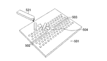
- a two-dimensional photonic crystal body 501 is formed with an optical waveguide 502 by a line defect, and a nanowire 504 is arranged in a groove 503 formed in the optical waveguide 502. It has a structure.
- the two-dimensional photonic crystal main body 501 is composed of a plate-shaped base portion 505 and a plurality of lattice elements 506 that are periodically provided on the base portion 505.
- the nanowire 504 is arranged in the groove 503 using the probe 521 of the atomic force microscope. Light is strongly confined at the portion of the groove 503 where the nanowire 504 is arranged.
- the nanowires are placed on the substrate.
- This technique includes a method using an inkjet method and a method using a micromanipulator. Further, in order to arrange the nanowire arranged on the substrate in the groove, the nanowire is manipulated by using the atomic force microscope, the optical tweezers or the micromanipulator described above. It is also possible to directly grow the nanowires of different materials on the silicon substrate so that the nanowires are arranged in the grooves.
- the technique for arranging nanowires in the grooves of the photonic crystal described above has achieved certain success in that it makes it possible to observe laser oscillation and quantum optical effects.
- -It is important to form an appropriate electrode structure, for example, a current injection structure, in the nanowire optical device using such a photonic crystal in order to realize future on-chip optical integrated devices.
- an appropriate electrode structure for example, a current injection structure
- the capacitance of the nanowire itself is very small, and thus the nanowire optical device can be operated at high speed.
- This nanowire optical device has an optical waveguide 502 provided in the photonic crystal body 501, a groove 503 formed in the optical waveguide 502, similar to the photonic crystal body 501 described with reference to FIGS. 9A and 9B.
- the photonic crystal body 501 includes a plate-shaped base 505 and a plurality of lattice elements 506.
- n-type region 507 is formed on one end side of the nanowire 504, and a p-type region 508 is formed on the other end side of the nanowire 504.
- N-type region 507 and p-type region 508 are formed by introducing corresponding impurities.
- an active region 509 is formed in a region sandwiched between the n-type region 507 and the p-type region 508 of the nanowire 504.
- the active region 509 has, for example, a multiple quantum well structure.
- a first electrode 510 made of metal is connected to the n-type region 507, and a second electrode 511 made of metal is connected to the p-type region 508.
- the first electrode 510 and the second electrode 511 are connected to a power source (not shown), a current is passed through the nanowire 504, and carriers are injected into the active region 509, so that the active region 509 can emit light.
- the detour optical waveguide 502a due to the line defect is provided, and the light generated in the active region 509 is guided to the detour optical waveguide 502a and extracted.
- the detour optical waveguide 502a even when the detour optical waveguide 502a is used, there is a problem that the guided light loss due to the detour optical waveguide 502a having the bending structure occurs and the band of the guided light becomes narrow. Further, in order to suppress the absorption of light by the electrode made of metal, the electrode is separated from the active region 509. However, the longer the distance between the electrode and the active region 509, the higher the resistance value between the active region 509 and the electrode, and the lower the efficiency of current injection.
- the present invention has been made to solve the above problems, and an object of the present invention is to suppress light loss in a nanowire optical device without increasing the distance between the active region and the electrode.
- the nanowire optical device comprises a base and a plurality of columnar grating elements having a refractive index different from that of the base, and the plurality of grating elements are periodically arranged on the base at intervals equal to or less than the wavelength of light of interest.
- a plate-shaped photonic crystal body provided in the optical waveguide, an optical waveguide by a line defect in which a plurality of defects composed of a portion without a lattice element of the photonic crystal body are linearly arranged, and a waveguide direction in the optical waveguide.
- the n-type region of the first electrode includes an active region sandwiched between an n-type region and a p-type region, a first electrode connected to the n-type region, and a second electrode connected to the p-type region. At least one of the region in contact with the p-type region and the region in contact with the p-type region of the second electrode is made of a transparent electrode material.
- the groove is formed to be wider than the width of the nanowire in a region formed of the transparent electrode material of at least one of the first electrode and the second electrode in plan view. Has been done.
- At least one of the region connected to the n-type region of the first electrode and the region connected to the p-type region of the second electrode is a nanowire region.
- the transparent electrode material is formed in contact with the side surface of the nanowire facing the side surface of the groove in addition to the upper surface of the transparent electrode material.
- the width of the groove becomes wider in a plan view in a region formed of the transparent electrode material of at least one of the first electrode and the second electrode, as the distance from the active region increases. ..
- the configuration example of the nanowire optical device further includes an optical confinement structure for confining light in the active region, and the optical confinement structure is formed by sandwiching the active region in an optical waveguide.
- At least one of the region connected to the n-type region of the first electrode and the region connected to the p-type region of the second electrode is made of the transparent electrode material. It is possible to obtain an excellent effect that the loss of light in the nanowire optical device can be suppressed without increasing the distance between the region and the electrode.
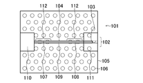
- FIG. 1A is a plan view showing the configuration of the nanowire optical device according to the first embodiment of the present invention.
- FIG. 1B is a sectional view showing the configuration of the nanowire optical device according to the first embodiment of the present invention.
- FIG. 2A is a plan view showing the configuration of the nanowire optical device according to the second embodiment of the present invention.
- FIG. 2B is a sectional view showing the configuration of the nanowire optical device according to the second embodiment of the present invention.
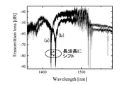
- FIG. 3 shows a case where a transparent electrode material made of ZnO having a thickness of several nm and a width of 5 ⁇ m is formed on the nanowire 104 arranged in the groove 103 (b) and a case where the transparent electrode material is not formed (a).
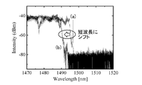
- FIG. 4 is a characteristic diagram showing the measurement results of the wavelength shift between the groove 103 having a width of 100 nm and (a) and the groove 103a having a width of 150 nm and (b).
- FIG. 5A is a plan view showing the configuration of another nanowire optical device according to the embodiment of the present invention.
- FIG. 5B is a plan view showing the configuration of another nanowire optical device according to the embodiment of the present invention.
- FIG. 5C is a plan view showing the configuration of another nanowire optical device according to the embodiment of the present invention.
- FIG. 6 is a plan view showing the configuration of another nanowire optical device according to the embodiment of the present invention.
- FIG. 7 is a plan view showing the configuration of another nanowire optical device according to the embodiment of the present invention.
- FIG. 8 is a plan view showing the configuration of another nanowire optical device according to the embodiment of the present invention.
- FIG. 9A is a perspective view showing a configuration of a conventional nanowire optical device.
- FIG. 9B is a plan view showing a configuration of a conventional nanowire optical device.
- FIG. 10 is a plan view showing a configuration of a conventional nanowire optical device.
- FIG. 1B shows a cross section taken along the line aa ′ in FIG. 1A.
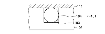
- This nanowire optical device includes a photonic crystal body 101, an optical waveguide 102 provided in the photonic crystal body 101, a groove 103 formed in the optical waveguide 102, and a nanowire 104 arranged in the groove 103.
- the photonic crystal body 101 can be made of, for example, silicon.
- the nanowire 104 is composed of a semiconductor.
- the nanowire 104 can be made of a compound semiconductor such as InP.
- the photonic crystal body 101 includes a plate-shaped base 105 and a plurality of lattice elements 106.
- the grating element 106 has a refractive index different from that of the base 105.
- the base 105 is made of, for example, InP, and the lattice element 106 is, for example, a cylindrical through hole.
- the plurality of lattice elements 106 are periodically provided at intervals equal to or less than the wavelength of the target light, and are arranged in a triangular lattice shape in plan view, for example.
- the optical waveguide 102 is composed of line defects.
- a line defect is a linear array of a plurality of defects (point defects) formed from a portion of the photonic crystal body 101 without the lattice element 106.
- the groove 103 extends in the waveguide direction of the optical waveguide 102 thus configured.
- An n-type region 107 is formed on one end side of the nanowire 104, and a p-type region 108 is formed on the other end side of the nanowire 104.
- the n-type region 107 and the p-type region 108 can be formed by introducing corresponding impurities.
- an active region 109 is formed in a region sandwiched between the n-type region 107 and the p-type region 108 of the nanowire 104.
- the active region 109 has, for example, a multiple quantum well structure.
- the active region 109 can be formed by forming a multiple quantum well structure in which quantum well layers made of InAsP and barrier layers made of InP are alternately stacked in the extending direction of the nanowires 104.
- a quantum well layer made of InAsP functions as an active layer.
- the nanowire optical device includes the first electrode 110 connected to the n-type region 107 and the second electrode 111 connected to the p-type region 108.
- the first electrode 110 is in contact with the upper surface of the n-type region 107 at the opening end of the groove 103.
- the second electrode 111 is in contact with the upper surface of the p-type region 108 at the open end of the groove 103.
- At least a region of the second electrode 111 that is in contact with the p-type region 108 is made of a transparent electrode material.
- the second electrode 111 may be entirely made of a transparent electrode material.
- the second electrode 111 made of a transparent electrode material can be arranged directly on the optical waveguide 102 or on the photonic crystal body 101.
- the transparent electrode material can be composed of, for example, ITO (Indium Tin Oxide) or ZnO. Note that at least the region of the first electrode 110 that is connected (contacted) with the n-type region 107 can be made of a transparent electrode material. Also in this case, the first electrode 110 may be wholly made of a transparent electrode material.
- the light generated in the active region 109 when the light generated in the active region 109 is guided through the optical waveguide 102 in the direction of the second electrode 111, the light is not absorbed by the second electrode 111 and is guided. No loss of wave light. Therefore, according to the first embodiment, the light generated in the active region 109 can be guided in the direction of the second electrode 111 of the optical waveguide 102 without the loss of the guided light. There is no need to introduce and there is no waveguide loss due to the use of bending waveguides.
- the second electrode 111 made of a transparent electrode material can be arranged close to the active region 109, and the resistance value between the active region 109 and the second electrode 111 can be lowered, so that the current injection The decrease in efficiency can be suppressed. It is also possible that at least a region of the second electrode 111 that influences the optical characteristics and that is connected (contacted) with the p-type region 108 is made of a transparent electrode material, and the other region of the second electrode 111 is made of a metal. Is. Although the transparent electrode material has a high resistivity with respect to a metal, by limiting the portion of the transparent electrode material to a portion that affects the optical characteristics and forming the other region from the metal, the overall resistance of the second electrode 111 can be reduced. Can be lowered. The same applies to the case where the first electrode 110 is made of a transparent electrode material. The light generated in the active region 109 can be guided in the direction of the first electrode 110 of the optical waveguide 102 without loss of guided light.
- the nanowire optical device according to the first embodiment can function as a light emitting element that causes the active region 109 to emit light by injecting a current into the active region 109 through the first electrode 110 and the second electrode 111, for example.
- the n-type region 107, the active region 109, and the p-type region 108 can function as a photodiode having a so-called pin structure.
- FIG. 2B shows a cross section taken along the line aa ′ of FIG. 2A.
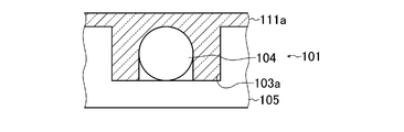
- the first electrode 110a connected to the n-type region 107 and the second electrode 111a connected to the p-type region 108 are provided. Further, at least a region of the second electrode 111a that is connected (contacted) with the p-type region 108 is made of a transparent electrode material.
- the width of the groove 103a is made wider than the width of the nanowire 104 in the region formed of the transparent electrode material in the region connected to the p-type region 108 of the second electrode 111a.
- the width of the groove 103b is made wider than the width of the nanowire 104 even in the region of the first electrode 110a connected to the n-type region 107.
- the region of the second electrode 111a made of the transparent electrode material is formed not only on the upper surface of the nanowire 104 but also on the side surface of the nanowire 104 facing the side surface of the groove 103a. It is formed in contact. Even when the first electrode 110a is made of a transparent electrode material, the region made of the transparent electrode material of the first electrode 110a is formed on the side surface of the nanowire 104 facing the side surface of the groove 103b in addition to the upper surface of the nanowire 104. It can be configured to be in contact with each other.
- the transparent electrode material is also in contact with the side surface of the nanowire 104 facing the side surface of the groove 103a, as compared with the state in which the second electrode 111a made of the transparent electrode material is connected (contacted) only on the upper surface of the nanowire 104. Therefore, the resistance value can be lowered.
- the electrode is formed by the vapor deposition method or the sputtering method, if the width of the groove 103a is made wider than the width of the nanowire 104, the electrode material can be deposited and formed on the side surface of the nanowire 104 as well.
- FIG. 3 shows the wavelength shift between the case where a transparent electrode material made of ZnO having a thickness of several nm and a width of 5 ⁇ m is formed on the nanowire 104 arranged in the groove 103 and the case where the transparent electrode material is not formed. The measurement results are shown.
- the case where the transparent electrode material is not formed (a)
- the case where the transparent electrode material is formed (b) has only a wavelength shift to the long wavelength side of about 20 nm.
- the wavelength shift is small and, as described above, the waveguide loss (transmission loss) is also small, so that the optical characteristics of the nanowire optical device are not significantly impaired.
- FIG. 4 shows the measurement results of the wavelength shift between the groove 103 having a width of 100 nm in plan view and the groove 103a having a width of 150 nm in plan view.
- the groove 103a (b) having a width of 150 nm shifts to the short wavelength side by only about 10 to 20 nm.
- the wavelength shift due to the increased width is small, and therefore the optical characteristics of the nanowire optical device are not significantly impaired.
- the wavelength shift to the short wavelength side is canceled by the wavelength shift to the long wavelength side, so that the transmission band can be narrowed. Absent.
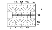
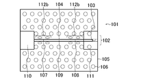
- a resonator can be formed by providing an optical confinement structure 112 for confining light in the active region 109 of the nanowire 104.
- the light confinement structure 112 may be formed by periodically disposing columnar structures having a refractive index different from that of the base 105 formed in the photonic crystal body 101 in the optical waveguide direction.
- the light confinement structure 112a may be a rectangular parallelepiped through hole.
- a light confinement structure 112b may be formed by a through hole arranged between the groove 103 and the row of the grating elements 106 adjacent to the optical waveguide 102.
- the grating element 106 a adjacent to the groove 103 is shifted in the direction away from the groove 103, so that the optics of this region are changed. It becomes possible to adjust the characteristics.
- the second electrode 111b made of a transparent electrode material can be arranged along the optical waveguide 102 on the inner side in the width direction of the optical waveguide 102 in plan view.
- the second electrode 111b is arranged between the two rows of the lattice elements 106 adjacent to the groove 103 and in parallel with the optical waveguide 102.
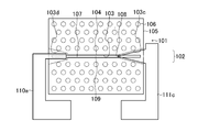
- the width of the groove 103c in the region connected to the p-type region of the second electrode 111c, can be made wider in a plan view as the distance from the active region 109 increases.
- the width of the groove 103d in the region of the first electrode 110a connected to the n-type region 107, can be made wider as it is farther from the active region 109 in a plan view.
- the groove 103c is formed in a region made of the transparent electrode material of the first electrode 110a in plan view.
- the groove 103d can also be formed in a region made of the transparent electrode material of the second electrode 111c in plan view.
- At least one of the region connected to the n-type region of the first electrode and the region connected to the p-type region of the second electrode is made of the transparent electrode material.
- the light loss in the nanowire optical device can be suppressed without increasing the distance between the active region and the electrode.
- 101 Photonic crystal body, 102 ... Optical waveguide, 103 ... Groove, 104 ... Nanowire, 105 ... Base, 106 ... Lattice element, 107 ... N-type region, 108 ... P-type region, 110 ... First electrode, 111 ... 2 electrodes.
Landscapes
- Physics & Mathematics (AREA)
- General Physics & Mathematics (AREA)
- Optics & Photonics (AREA)
- Condensed Matter Physics & Semiconductors (AREA)
- Electromagnetism (AREA)
- Engineering & Computer Science (AREA)
- Microelectronics & Electronic Packaging (AREA)
- Nonlinear Science (AREA)
- Optical Integrated Circuits (AREA)
- Semiconductor Lasers (AREA)
Abstract
La présente invention concerne un dispositif optique à nanofils comprenant : un corps de cristal photonique de type plaque disposé sur un substrat ; un guide d'ondes optiques composé d'une pluralité de défauts de ligne disposés linéairement constitués de parties sans éléments de réseau du corps de cristal photonique ; une rainure formée dans le guide d'ondes optiques le long de la direction de guide d'ondes ; un nanofil réalisé à partir d'un semi-conducteur et disposé dans la rainure ; une région de type n formée à une extrémité du nanofil ; une région de type p formée à l'autre extrémité du nanofil ; une région active formée entre la région de type n et la région de type p du nanofil ; une première électrode connectée à la région de type n ; et une seconde électrode connectée à la région de type p. Au moins une région en contact avec la région de type n de la première électrode ou une région en contact avec la région de type p de la seconde électrode est constituée d'un matériau d'électrode transparent.
Priority Applications (1)
| Application Number | Priority Date | Filing Date | Title |
|---|---|---|---|
| US17/293,399 US12155012B2 (en) | 2018-11-14 | 2019-10-31 | Nanowire optical device |
Applications Claiming Priority (2)
| Application Number | Priority Date | Filing Date | Title |
|---|---|---|---|
| JP2018213551A JP2020080389A (ja) | 2018-11-14 | 2018-11-14 | ナノワイヤ光デバイス |
| JP2018-213551 | 2018-11-14 |
Publications (1)
| Publication Number | Publication Date |
|---|---|
| WO2020100611A1 true WO2020100611A1 (fr) | 2020-05-22 |
Family
ID=70731504
Family Applications (1)
| Application Number | Title | Priority Date | Filing Date |
|---|---|---|---|
| PCT/JP2019/042779 Ceased WO2020100611A1 (fr) | 2018-11-14 | 2019-10-31 | Dispositif optique à nanofils |
Country Status (3)
| Country | Link |
|---|---|
| US (1) | US12155012B2 (fr) |
| JP (1) | JP2020080389A (fr) |
| WO (1) | WO2020100611A1 (fr) |
Cited By (1)
| Publication number | Priority date | Publication date | Assignee | Title |
|---|---|---|---|---|
| JPWO2023152873A1 (fr) * | 2022-02-10 | 2023-08-17 |
Families Citing this family (1)
| Publication number | Priority date | Publication date | Assignee | Title |
|---|---|---|---|---|
| JP7664388B2 (ja) * | 2020-10-30 | 2025-04-17 | クオンタム ヴァリー アイデアズ ラボラトリーズ | 高周波電磁放射の生成 |
Citations (9)
| Publication number | Priority date | Publication date | Assignee | Title |
|---|---|---|---|---|
| WO2007074876A1 (fr) * | 2005-12-27 | 2007-07-05 | Nec Corporation | Structure de couplage de guide d’onde |
| US7474811B1 (en) * | 2007-09-14 | 2009-01-06 | Hewlett-Packard Development Company, L.P. | Nanowire photonic apparatus employing optical field confinement |
| JP2009505415A (ja) * | 2005-08-19 | 2009-02-05 | ポステック・ファウンデーション | 伝導性ナノロッドを透明電極として含む発光素子 |
| JP2009088481A (ja) * | 2007-09-14 | 2009-04-23 | Sharp Corp | 窒化物半導体発光素子 |
| US7603016B1 (en) * | 2007-04-30 | 2009-10-13 | The United States Of America As Represented By The Secretary Of The Air Force | Semiconductor photonic nano communication link apparatus |
| JP2014027168A (ja) * | 2012-07-27 | 2014-02-06 | Nippon Telegr & Teleph Corp <Ntt> | フォトニック結晶共振器の作製方法およびフォトニック結晶共振器 |
| JP2016115783A (ja) * | 2014-12-15 | 2016-06-23 | 日本電信電話株式会社 | 光素子 |
| JP2016154164A (ja) * | 2015-02-20 | 2016-08-25 | 日本電信電話株式会社 | フォトニック結晶共振器およびその設計方法 |
| JP2018032751A (ja) * | 2016-08-25 | 2018-03-01 | 日本電信電話株式会社 | ナノワイヤレーザ |
Family Cites Families (5)
| Publication number | Priority date | Publication date | Assignee | Title |
|---|---|---|---|---|
| US7847312B2 (en) | 2007-09-14 | 2010-12-07 | Sharp Kabushiki Kaisha | Nitride semiconductor light-emitting device |
| FR2968776B1 (fr) * | 2010-12-13 | 2012-12-28 | Commissariat Energie Atomique | Procédé pour réaliser un guide optique a fente sur silicium |
| GB201613791D0 (en) * | 2016-08-11 | 2016-09-28 | Univ Southampton | Optical structure and method of fabricating an optical structure |
| EP3418784B1 (fr) * | 2017-06-21 | 2021-09-08 | ADVA Optical Networking SE | Dispositif optique/puce photonique permettant d'aligner et de connecter une fibre optique et un guide d'onde photonique intégré et son procédé de production |
| DE102021211848A1 (de) * | 2021-10-20 | 2023-04-20 | Fraunhofer-Gesellschaft zur Förderung der angewandten Forschung eingetragener Verein | Vorrichtung zur erzeugung einer laserstrahlung mit einer lateral-current-injection-laseranordnung und einem hohlraum, sowie verfahren zur herstellung derselben |
-
2018
- 2018-11-14 JP JP2018213551A patent/JP2020080389A/ja active Pending
-
2019
- 2019-10-31 WO PCT/JP2019/042779 patent/WO2020100611A1/fr not_active Ceased
- 2019-10-31 US US17/293,399 patent/US12155012B2/en active Active
Patent Citations (9)
| Publication number | Priority date | Publication date | Assignee | Title |
|---|---|---|---|---|
| JP2009505415A (ja) * | 2005-08-19 | 2009-02-05 | ポステック・ファウンデーション | 伝導性ナノロッドを透明電極として含む発光素子 |
| WO2007074876A1 (fr) * | 2005-12-27 | 2007-07-05 | Nec Corporation | Structure de couplage de guide d’onde |
| US7603016B1 (en) * | 2007-04-30 | 2009-10-13 | The United States Of America As Represented By The Secretary Of The Air Force | Semiconductor photonic nano communication link apparatus |
| US7474811B1 (en) * | 2007-09-14 | 2009-01-06 | Hewlett-Packard Development Company, L.P. | Nanowire photonic apparatus employing optical field confinement |
| JP2009088481A (ja) * | 2007-09-14 | 2009-04-23 | Sharp Corp | 窒化物半導体発光素子 |
| JP2014027168A (ja) * | 2012-07-27 | 2014-02-06 | Nippon Telegr & Teleph Corp <Ntt> | フォトニック結晶共振器の作製方法およびフォトニック結晶共振器 |
| JP2016115783A (ja) * | 2014-12-15 | 2016-06-23 | 日本電信電話株式会社 | 光素子 |
| JP2016154164A (ja) * | 2015-02-20 | 2016-08-25 | 日本電信電話株式会社 | フォトニック結晶共振器およびその設計方法 |
| JP2018032751A (ja) * | 2016-08-25 | 2018-03-01 | 日本電信電話株式会社 | ナノワイヤレーザ |
Non-Patent Citations (5)
| Title |
|---|
| BIROWOSUTO, ET AL: "Position Controlled Nanocavity Using a Single Nanowire in Photonic Crystals", 2013 CONFERENCE ON LASERS AND ELECTRO-OPTICS PACIFIC RIM, 30 June 2013 (2013-06-30), XP032481409 * |
| DANANG BIROWOSUTO MUHAMMAD ET AL: "Design for ultrahigh-Q position-controlled nanocavities of single semiconductor nanowires in two-dimensional photonic crystals", JOURNAL OF APPLIED PHYSICS, vol. 112, 113106, 6 December 2012 (2012-12-06), pages 1 - 10, XP012167100, ISSN: 0021-8979, DOI: 10.1063/1.4768437 * |
| MASATO TAKIGUCHI ET AL: "Continuous-wave operation and 10-Gb/s direct modulation of InAsP/InP sub-wavelength nanowire laser on silicon photonic crystal", APL PHOTONICS, vol. 2, no. 4, 3 April 2017 (2017-04-03), pages 1 - 10, XP012217649, DOI: 10.1063/1.4977927 * |
| MASATO TAKIGUCHI ET AL: "Movable Nanowire Laser On Silicon Photonic Crystal Using Atomic Force Microscopy", 2018 INTERNATIONAL CONFERENCE ON MANIPULATION, AUTOMATION AND ROBOTICS AT SMALL SCALES (MARSS), 4 July 2018 (2018-07-04), pages 1 - 4, XP033413146, DOI: 10.1109/MARSS.2018.8481227 * |
| YOKOO ET AL: "Semiconductor Nanowire Induced Photonic-Crystal Nanocavity with Selectable Resonant Wavelength, 2014 Conference on Lasers and Electro- Optics (CLEO", 2014 CONFERENCE ON LASERS AND ELECTRO-OPTICS (CLEO) - LASER SCIENCE TO PHOTONIC APPLICATIONS, 8 June 2014 (2014-06-08), pages 1 - 2, XP032707697, DOI: 10.1364/CLEO_SI.2014.STu2H.5 * |
Cited By (3)
| Publication number | Priority date | Publication date | Assignee | Title |
|---|---|---|---|---|
| JPWO2023152873A1 (fr) * | 2022-02-10 | 2023-08-17 | ||
| WO2023152873A1 (fr) * | 2022-02-10 | 2023-08-17 | 日本電信電話株式会社 | Procédé de fabrication d'un dispositif à nanostructure |
| JP7747078B2 (ja) | 2022-02-10 | 2025-10-01 | Ntt株式会社 | ナノ構造デバイスの作製方法 |
Also Published As
| Publication number | Publication date |
|---|---|
| JP2020080389A (ja) | 2020-05-28 |
| US12155012B2 (en) | 2024-11-26 |
| US20210408336A1 (en) | 2021-12-30 |
Similar Documents
| Publication | Publication Date | Title |
|---|---|---|
| US7263251B2 (en) | Optical switch having photonic crystal structure | |
| US9893493B2 (en) | Surface emitting quantum cascade laser | |
| CN100593889C (zh) | 垂直腔表面发射激光器 | |
| KR100792078B1 (ko) | 2차원 포토닉 결정면 발광레이저 | |
| JPWO2003067724A1 (ja) | 半導体発光素子およびその製造方法 | |
| US20080273832A1 (en) | Photonic crystal optical device | |
| JP7293348B2 (ja) | 位相結合されたレーザ装置、および位相結合されたレーザ装置を製造するための方法 | |
| WO2013183178A1 (fr) | Détecteur optique | |
| JP2011091164A (ja) | 半導体集積素子 | |
| TWI791217B (zh) | 光子晶體面射型雷射元件 | |
| JP2005159002A (ja) | 受光素子、光モジュール、及び光伝送装置 | |
| CN115882339A (zh) | 包含多主动层与光栅层的半导体激光二极体 | |
| JP4445292B2 (ja) | 半導体発光素子 | |
| JP2011091163A (ja) | 半導体集積素子 | |
| JP6669611B2 (ja) | ナノワイヤレーザ | |
| US12155012B2 (en) | Nanowire optical device | |
| KR102366164B1 (ko) | 마흐-젠더 전기 광학 변조기 및 이의 제조 방법 | |
| JP2012093584A (ja) | 光カプラ、光走査装置、分光装置、 | |
| JP4386191B2 (ja) | 光素子 | |
| JP6162465B2 (ja) | 半導体レーザ装置 | |
| JP5309877B2 (ja) | フォトニック結晶面発光レーザ素子 | |
| US10511148B2 (en) | Tunable laser device | |
| AT511032B1 (de) | Zweidimensionales distributed-feedback halbleiter laser array | |
| JP6808336B2 (ja) | 半導体レーザ装置 | |
| JP2013197502A (ja) | 変調器集積半導体レーザ |
Legal Events
| Date | Code | Title | Description |
|---|---|---|---|
| 121 | Ep: the epo has been informed by wipo that ep was designated in this application |
Ref document number: 19885565 Country of ref document: EP Kind code of ref document: A1 |
|
| NENP | Non-entry into the national phase |
Ref country code: DE |
|
| 122 | Ep: pct application non-entry in european phase |
Ref document number: 19885565 Country of ref document: EP Kind code of ref document: A1 |