WO2020111094A1 - 電気化学デバイス用負極および電気化学デバイス、並びに電気化学デバイス用負極の製造方法および電気化学デバイスの製造方法 - Google Patents
電気化学デバイス用負極および電気化学デバイス、並びに電気化学デバイス用負極の製造方法および電気化学デバイスの製造方法 Download PDFInfo
- Publication number
- WO2020111094A1 WO2020111094A1 PCT/JP2019/046294 JP2019046294W WO2020111094A1 WO 2020111094 A1 WO2020111094 A1 WO 2020111094A1 JP 2019046294 W JP2019046294 W JP 2019046294W WO 2020111094 A1 WO2020111094 A1 WO 2020111094A1
- Authority
- WO
- WIPO (PCT)
- Prior art keywords
- negative electrode
- material layer
- electrochemical device
- positive electrode
- peak
- Prior art date
- Legal status (The legal status is an assumption and is not a legal conclusion. Google has not performed a legal analysis and makes no representation as to the accuracy of the status listed.)
- Ceased
Links
Images
Classifications
-
- H—ELECTRICITY
- H01—ELECTRIC ELEMENTS
- H01G—CAPACITORS; CAPACITORS, RECTIFIERS, DETECTORS, SWITCHING DEVICES, LIGHT-SENSITIVE OR TEMPERATURE-SENSITIVE DEVICES OF THE ELECTROLYTIC TYPE
- H01G11/00—Hybrid capacitors, i.e. capacitors having different positive and negative electrodes; Electric double-layer [EDL] capacitors; Processes for the manufacture thereof or of parts thereof
- H01G11/04—Hybrid capacitors
- H01G11/06—Hybrid capacitors with one of the electrodes allowing ions to be reversibly doped thereinto, e.g. lithium ion capacitors [LIC]
-
- H—ELECTRICITY
- H01—ELECTRIC ELEMENTS
- H01G—CAPACITORS; CAPACITORS, RECTIFIERS, DETECTORS, SWITCHING DEVICES, LIGHT-SENSITIVE OR TEMPERATURE-SENSITIVE DEVICES OF THE ELECTROLYTIC TYPE
- H01G11/00—Hybrid capacitors, i.e. capacitors having different positive and negative electrodes; Electric double-layer [EDL] capacitors; Processes for the manufacture thereof or of parts thereof
- H01G11/22—Electrodes
- H01G11/30—Electrodes characterised by their material
- H01G11/32—Carbon-based
-
- H—ELECTRICITY
- H01—ELECTRIC ELEMENTS
- H01G—CAPACITORS; CAPACITORS, RECTIFIERS, DETECTORS, SWITCHING DEVICES, LIGHT-SENSITIVE OR TEMPERATURE-SENSITIVE DEVICES OF THE ELECTROLYTIC TYPE
- H01G11/00—Hybrid capacitors, i.e. capacitors having different positive and negative electrodes; Electric double-layer [EDL] capacitors; Processes for the manufacture thereof or of parts thereof
- H01G11/22—Electrodes
- H01G11/30—Electrodes characterised by their material
- H01G11/48—Conductive polymers
-
- H—ELECTRICITY
- H01—ELECTRIC ELEMENTS
- H01G—CAPACITORS; CAPACITORS, RECTIFIERS, DETECTORS, SWITCHING DEVICES, LIGHT-SENSITIVE OR TEMPERATURE-SENSITIVE DEVICES OF THE ELECTROLYTIC TYPE
- H01G11/00—Hybrid capacitors, i.e. capacitors having different positive and negative electrodes; Electric double-layer [EDL] capacitors; Processes for the manufacture thereof or of parts thereof
- H01G11/22—Electrodes
- H01G11/30—Electrodes characterised by their material
- H01G11/50—Electrodes characterised by their material specially adapted for lithium-ion capacitors, e.g. for lithium-doping or for intercalation
-
- H—ELECTRICITY
- H01—ELECTRIC ELEMENTS
- H01G—CAPACITORS; CAPACITORS, RECTIFIERS, DETECTORS, SWITCHING DEVICES, LIGHT-SENSITIVE OR TEMPERATURE-SENSITIVE DEVICES OF THE ELECTROLYTIC TYPE
- H01G11/00—Hybrid capacitors, i.e. capacitors having different positive and negative electrodes; Electric double-layer [EDL] capacitors; Processes for the manufacture thereof or of parts thereof
- H01G11/52—Separators
-
- H—ELECTRICITY
- H01—ELECTRIC ELEMENTS
- H01G—CAPACITORS; CAPACITORS, RECTIFIERS, DETECTORS, SWITCHING DEVICES, LIGHT-SENSITIVE OR TEMPERATURE-SENSITIVE DEVICES OF THE ELECTROLYTIC TYPE
- H01G11/00—Hybrid capacitors, i.e. capacitors having different positive and negative electrodes; Electric double-layer [EDL] capacitors; Processes for the manufacture thereof or of parts thereof
- H01G11/84—Processes for the manufacture of hybrid or EDL capacitors, or components thereof
- H01G11/86—Processes for the manufacture of hybrid or EDL capacitors, or components thereof specially adapted for electrodes
-
- H—ELECTRICITY
- H01—ELECTRIC ELEMENTS
- H01M—PROCESSES OR MEANS, e.g. BATTERIES, FOR THE DIRECT CONVERSION OF CHEMICAL ENERGY INTO ELECTRICAL ENERGY
- H01M10/00—Secondary cells; Manufacture thereof
- H01M10/05—Accumulators with non-aqueous electrolyte
- H01M10/052—Li-accumulators
-
- H—ELECTRICITY
- H01—ELECTRIC ELEMENTS
- H01M—PROCESSES OR MEANS, e.g. BATTERIES, FOR THE DIRECT CONVERSION OF CHEMICAL ENERGY INTO ELECTRICAL ENERGY
- H01M4/00—Electrodes
- H01M4/02—Electrodes composed of, or comprising, active material
- H01M4/36—Selection of substances as active materials, active masses, active liquids
- H01M4/362—Composites
- H01M4/366—Composites as layered products
-
- H—ELECTRICITY
- H01—ELECTRIC ELEMENTS
- H01M—PROCESSES OR MEANS, e.g. BATTERIES, FOR THE DIRECT CONVERSION OF CHEMICAL ENERGY INTO ELECTRICAL ENERGY
- H01M4/00—Electrodes
- H01M4/02—Electrodes composed of, or comprising, active material
- H01M4/36—Selection of substances as active materials, active masses, active liquids
- H01M4/38—Selection of substances as active materials, active masses, active liquids of elements or alloys
- H01M4/381—Alkaline or alkaline earth metals elements
- H01M4/382—Lithium
-
- H—ELECTRICITY
- H01—ELECTRIC ELEMENTS
- H01M—PROCESSES OR MEANS, e.g. BATTERIES, FOR THE DIRECT CONVERSION OF CHEMICAL ENERGY INTO ELECTRICAL ENERGY
- H01M4/00—Electrodes
- H01M4/02—Electrodes composed of, or comprising, active material
- H01M4/36—Selection of substances as active materials, active masses, active liquids
- H01M4/58—Selection of substances as active materials, active masses, active liquids of inorganic compounds other than oxides or hydroxides, e.g. sulfides, selenides, tellurides, halogenides or LiCoFy; of polyanionic structures, e.g. phosphates, silicates or borates
- H01M4/583—Carbonaceous material, e.g. graphite-intercalation compounds or CFx
-
- H—ELECTRICITY
- H01—ELECTRIC ELEMENTS
- H01G—CAPACITORS; CAPACITORS, RECTIFIERS, DETECTORS, SWITCHING DEVICES, LIGHT-SENSITIVE OR TEMPERATURE-SENSITIVE DEVICES OF THE ELECTROLYTIC TYPE
- H01G11/00—Hybrid capacitors, i.e. capacitors having different positive and negative electrodes; Electric double-layer [EDL] capacitors; Processes for the manufacture thereof or of parts thereof
- H01G11/54—Electrolytes
- H01G11/58—Liquid electrolytes
- H01G11/62—Liquid electrolytes characterised by the solute, e.g. salts, anions or cations therein
-
- H—ELECTRICITY
- H01—ELECTRIC ELEMENTS
- H01M—PROCESSES OR MEANS, e.g. BATTERIES, FOR THE DIRECT CONVERSION OF CHEMICAL ENERGY INTO ELECTRICAL ENERGY
- H01M4/00—Electrodes
- H01M4/02—Electrodes composed of, or comprising, active material
- H01M2004/026—Electrodes composed of, or comprising, active material characterised by the polarity
- H01M2004/027—Negative electrodes
-
- H—ELECTRICITY
- H01—ELECTRIC ELEMENTS
- H01M—PROCESSES OR MEANS, e.g. BATTERIES, FOR THE DIRECT CONVERSION OF CHEMICAL ENERGY INTO ELECTRICAL ENERGY
- H01M2300/00—Electrolytes
- H01M2300/0017—Non-aqueous electrolytes
- H01M2300/0025—Organic electrolyte
- H01M2300/0028—Organic electrolyte characterised by the solvent
- H01M2300/0037—Mixture of solvents
-
- H—ELECTRICITY
- H01—ELECTRIC ELEMENTS
- H01M—PROCESSES OR MEANS, e.g. BATTERIES, FOR THE DIRECT CONVERSION OF CHEMICAL ENERGY INTO ELECTRICAL ENERGY
- H01M2300/00—Electrolytes
- H01M2300/0017—Non-aqueous electrolytes
- H01M2300/0025—Organic electrolyte
- H01M2300/0028—Organic electrolyte characterised by the solvent
- H01M2300/0037—Mixture of solvents
- H01M2300/004—Three solvents
-
- H—ELECTRICITY
- H01—ELECTRIC ELEMENTS
- H01M—PROCESSES OR MEANS, e.g. BATTERIES, FOR THE DIRECT CONVERSION OF CHEMICAL ENERGY INTO ELECTRICAL ENERGY
- H01M4/00—Electrodes
- H01M4/02—Electrodes composed of, or comprising, active material
- H01M4/36—Selection of substances as active materials, active masses, active liquids
- H01M4/58—Selection of substances as active materials, active masses, active liquids of inorganic compounds other than oxides or hydroxides, e.g. sulfides, selenides, tellurides, halogenides or LiCoFy; of polyanionic structures, e.g. phosphates, silicates or borates
- H01M4/583—Carbonaceous material, e.g. graphite-intercalation compounds or CFx
- H01M4/587—Carbonaceous material, e.g. graphite-intercalation compounds or CFx for inserting or intercalating light metals
-
- Y—GENERAL TAGGING OF NEW TECHNOLOGICAL DEVELOPMENTS; GENERAL TAGGING OF CROSS-SECTIONAL TECHNOLOGIES SPANNING OVER SEVERAL SECTIONS OF THE IPC; TECHNICAL SUBJECTS COVERED BY FORMER USPC CROSS-REFERENCE ART COLLECTIONS [XRACs] AND DIGESTS
- Y02—TECHNOLOGIES OR APPLICATIONS FOR MITIGATION OR ADAPTATION AGAINST CLIMATE CHANGE
- Y02E—REDUCTION OF GREENHOUSE GAS [GHG] EMISSIONS, RELATED TO ENERGY GENERATION, TRANSMISSION OR DISTRIBUTION
- Y02E60/00—Enabling technologies; Technologies with a potential or indirect contribution to GHG emissions mitigation
- Y02E60/10—Energy storage using batteries
-
- Y—GENERAL TAGGING OF NEW TECHNOLOGICAL DEVELOPMENTS; GENERAL TAGGING OF CROSS-SECTIONAL TECHNOLOGIES SPANNING OVER SEVERAL SECTIONS OF THE IPC; TECHNICAL SUBJECTS COVERED BY FORMER USPC CROSS-REFERENCE ART COLLECTIONS [XRACs] AND DIGESTS
- Y02—TECHNOLOGIES OR APPLICATIONS FOR MITIGATION OR ADAPTATION AGAINST CLIMATE CHANGE
- Y02P—CLIMATE CHANGE MITIGATION TECHNOLOGIES IN THE PRODUCTION OR PROCESSING OF GOODS
- Y02P70/00—Climate change mitigation technologies in the production process for final industrial or consumer products
- Y02P70/50—Manufacturing or production processes characterised by the final manufactured product
Definitions
- the present invention relates to a negative electrode for an electrochemical device, an electrochemical device, a method for manufacturing a negative electrode for an electrochemical device, and a method for manufacturing an electrochemical device.
- Patent Documents 1 to 3 An electrochemical device using a carbon material in which lithium ions are occluded in the negative electrode material layer is known (see Patent Documents 1 to 3).
- a solid electrolyte interface coating (that is, SEI coating) is formed on the negative electrode material layer during charge/discharge.
- SEI coating plays an important role in the charge/discharge reaction, if the SEI film is formed excessively thick, the internal resistance of the electrochemical device increases.
- One aspect of the present invention comprises a negative electrode core material and a negative electrode material layer supported on the negative electrode core material, the negative electrode material layer contains a carbon material, and a surface layer portion of the negative electrode material layer is a lithium carbonate-containing region. And a negative electrode for an electrochemical device.
- the thickness of the lithium carbonate-containing region is, for example, 1 nm or more and 100 nm or less.
- Another aspect of the present invention is a positive electrode comprising a positive electrode core material and a positive electrode material layer carried on the positive electrode core material, the negative electrode, a separator interposed between the positive electrode and the negative electrode, an electrolyte,
- An electrochemical device comprising:
- Yet another aspect of the present invention comprises a step of preparing a negative electrode including a negative electrode core material and a negative electrode material layer carried on the negative electrode core material, the negative electrode material layer containing a carbon material, and the surface of the negative electrode material layer. And a step of depositing metallic lithium on the negative electrode, and exposing the negative electrode having the negative electrode material layer to which the metallic lithium is deposited to a carbon dioxide gas atmosphere to form a surface layer portion having a lithium carbonate-containing region with a thickness of 1 nm or more and 100 nm or less. And a step of forming the negative electrode material layer on the negative electrode material layer.
- Yet another aspect of the present invention comprises a step of preparing a negative electrode including a negative electrode core material and a negative electrode material layer carried on the negative electrode core material, the negative electrode material layer containing a carbon material, and the surface of the negative electrode material layer. And a step of preparing a positive electrode having a positive electrode core material and a positive electrode material layer carried on the positive electrode core material; and the negative electrode having the negative electrode material layer having the metallic lithium deposited thereon.
- the present invention relates to a method for manufacturing an electrochemical device, which includes a step of forming an electrode body with a separator interposed between the positive electrode and the positive electrode, and a step of exposing the electrode body to a carbon dioxide atmosphere.
- an increase in internal resistance of an electrochemical device can be effectively suppressed.
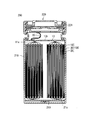
- FIG. 1 is a vertical cross-sectional view showing the configuration of an electrochemical device according to an embodiment of the present invention.
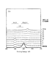
- FIG. 2 is a diagram showing a C1s spectrum in an XPS analysis of a lithium carbonate-containing region having a thickness of 30 nm.
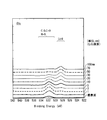
- FIG. 3 is a diagram showing an O1s spectrum in an XPS analysis of a lithium carbonate-containing region having a thickness of 30 nm.
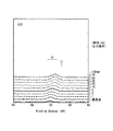
- FIG. 4 is a diagram showing a Li1s spectrum in an XPS analysis of a lithium carbonate-containing region having a thickness of 30 nm.
- the negative electrode for an electrochemical device includes a negative electrode core material and a negative electrode material layer carried on the negative electrode core material, and the negative electrode material layer contains a carbon material.
- the surface layer portion of the negative electrode material layer is composed of a coating film formed on the surface of the carbon material, and the coating film contains lithium carbonate. That is, a lithium carbonate-containing region exists in the surface layer portion of the negative electrode material layer.
- the lithium carbonate-containing region is, for example, a surface layer portion or a film region in which substantial presence of lithium carbonate is observed by analysis by X-ray photoelectron spectroscopy (XPS). The analysis method is not limited to XPS.
- the lithium carbonate-containing region is formed as a surface layer portion of the negative electrode material layer before assembling the electrochemical device. If the preformed lithium carbonate-containing region has a sufficient thickness, then in an electrochemical device assembled with the negative electrode, subsequent charge/discharge will result in a uniform and moderately thick SEI on the surface of the negative electrode material layer. It is considered that a film is formed. Therefore, the increase in internal resistance of the electrochemical device is reduced.
- the sufficient thickness may be, for example, 1 nm or more, and may be 5 nm or more in the case of expecting a longer-term action, and may be 30 nm or more in the case of expecting a more reliable action.
- the thickness of the lithium carbonate-containing region exceeds 100 nm, the lithium carbonate-containing region itself becomes a resistance component and the internal resistance of the electrochemical device increases. Therefore, the thickness of the lithium carbonate-containing region may be 100 nm or less.
- the thickness of the lithium carbonate-containing region is measured by analyzing the surface layer portion of the negative electrode material layer at multiple points (at least 5 points) of the negative electrode material layer. Then, the average of the thicknesses of the lithium carbonate-containing regions obtained at a plurality of points may be the thickness of the lithium carbonate-containing region.
- the negative electrode material layer provided for the measurement sample may be peeled off from the negative electrode core material. In this case, the coating film formed on the surface of the carbon material forming the vicinity of the surface layer portion of the negative electrode material layer may be analyzed. In this case, the carbon material covered with the coating may be collected and used for analysis from the region of the negative electrode material layer arranged on the surface side opposite to the surface bonded to the negative electrode core material.
- XPS analysis of the surface layer portion of the negative electrode material layer is performed, for example, by irradiating the coating formed on the surface layer portion or the surface of the carbon material with an argon beam in a chamber of an X-ray photoelectron spectrometer, and assigning C1s or O1s electrons to the irradiation time. Observe and record the change in each spectrum that is recorded. At this time, from the viewpoint of avoiding an analysis error, the spectrum of the outermost surface of the surface layer portion may be ignored.
- the thickness of the region where the peak attributed to lithium carbonate is stably observed corresponds to the thickness of the lithium carbonate-containing region.
- the coating formed on the surface layer portion of the negative electrode material layer or the surface of the carbon material is the SEI coating generated in the electrochemical device.
- An O1s peak attributed to lithium carbonate can also be observed in the SEI film.
- the SEI coating formed in the electrochemical device has a different composition from the preformed lithium carbonate-containing region, they can be distinguished from each other.
- the F1s peak attributed to the LiF bond is observed, but the substantial F1s peak attributed to the LiF bond is not observed in the lithium carbonate-containing region.
- the amount of lithium carbonate contained in the SEI film is very small.
- the Li1s peak for example, peaks derived from compounds such as ROCO 2 Li and ROLi can be detected.
- a second peak of O1s attributed to a Li—O bond may be observed in addition to the first peak of O1s attributed to a C ⁇ O bond.
- the region of the coating existing near the surface of the carbon material is considered to contain a slight amount of LiOH or Li 2 O.
- the first peak and the second peak are observed in the order of increasing distance from the outermost surface of the surface layer portion, and the first peak intensity May be observed in the first region, where the second peak intensity is greater than the second peak intensity, and in which the first peak and the second peak are observed and the second peak intensity is greater than the first peak intensity.
- the magnitude of the peak intensity may be determined by the height of the peak from the baseline.
- the C1s peak attributed to the CC bond is not substantially observed, or even if observed, it is less than half of the peak intensity attributed to the C ⁇ O bond. Is.
- an electrochemical device is a positive electrode including a positive electrode core material and a positive electrode material layer supported on the positive electrode core material, the negative electrode, and a separator interposed between the positive electrode and the negative electrode. And an electrolyte.
- the negative electrode and the positive electrode form an electrode body together with a separator interposed therebetween.
- the electrode body is configured as, for example, a column-shaped wound body in which a strip-shaped positive electrode and a negative electrode are wound via a separator. Further, the electrode body may be configured as a laminated body by laminating a plate-shaped positive electrode and a negative electrode with a separator interposed therebetween.
- the positive electrode material layer contains, for example, a conductive polymer as a positive electrode material.
- a conductive polymer for example, polyaniline or its derivative can be used.
- electrochemical devices utilizing lithium ions electrochemical devices in which the positive electrode material layer contains a conductive polymer and the negative electrode material layer contains a carbon material are expected to be used in various fields such as in-vehicle applications.
- lithium ions in the electrolyte are occluded in the negative electrode and anions are adsorbed (doped) in the positive electrode.
- lithium ions are released from the negative electrode into the electrolyte and anions are desorbed (dedoped) from the positive electrode into the electrolyte.
- the conductive polymer charges and discharges by doping and dedoping anions, so that the reaction resistance is small and it is easy to achieve high output.
- the conductive polymer is an organic substance, has low heat resistance, and can be dissolved in a solvent having a strong electrolyte polarity.
- the solvent in the electrolyte may decompose by a side reaction to produce alcohol.
- Conducting polymers such as polyaniline are susceptible to alcohol.
- the non-aqueous electrolyte solution decomposes on the negative electrode, and the decomposed product may react with the water in the non-aqueous electrolyte solution to generate a trace amount of alcohol. Alcohol may dissolve polyaniline.
- a lithium carbonate-containing region having a sufficient thickness is present in the surface layer portion of the negative electrode material layer, alcohol production is suppressed.
- the anion includes, for example, a fluorine-containing anion.
- An electrolyte salt having such an anion has a high degree of dissociation and provides an electrolytic solution having a low viscosity. Further, by including the fluorine-containing anion in the electrolyte, the withstand voltage characteristics of the electrochemical device can be improved.
- a method for manufacturing a negative electrode for an electrochemical device comprises a negative electrode core material and a negative electrode material layer carried on the negative electrode core material, and the negative electrode material layer prepares a negative electrode containing a carbon material.
- First step a second step of depositing metallic lithium on the surface of the negative electrode material layer, and a negative electrode having a negative electrode material layer having metallic lithium deposited thereon is exposed to a carbon dioxide gas atmosphere to form a carbon dioxide film having a thickness of 1 nm or more and 100 nm or less. It has a 3rd process of forming the surface layer part which has a lithium content field in a negative electrode material layer.
- the lithium carbonate-containing region in the surface layer portion of the negative electrode material layer is formed through the second step and the third step.
- the second step of depositing metallic lithium on the surface of the negative electrode material layer can be performed by, for example, a vapor phase method, transfer or the like.
- the vapor phase method include chemical vapor deposition, physical vapor deposition, and sputtering.
- metallic lithium may be formed into a film on the surface of the negative electrode material layer by a vacuum vapor deposition device.
- the pressure in the apparatus chamber during vapor deposition may be, for example, 10 ⁇ 2 to 10 ⁇ 5 Pa
- the temperature of the lithium evaporation source may be 400 to 600° C.
- the temperature of the negative electrode material layer may be ⁇ 20 to 80° C.
- the carbon dioxide gas atmosphere is a dry atmosphere containing no water, for example, a dew point of -40°C or lower or -50°C or lower.
- the carbon dioxide atmosphere may contain a gas other than carbon dioxide, but the carbon dioxide mole fraction is preferably 80% or more, and more preferably 95% or more. It is desirable not to include an oxidizing gas, and the oxygen mole fraction may be 0.1% or less.
- the partial pressure of carbon dioxide In order to form the lithium carbonate-containing region thicker, it is efficient to make the partial pressure of carbon dioxide larger than, for example, 0.5 atm (5.05 ⁇ 10 4 Pa), and 1 atm (1.01 ⁇ 10 4 ). 5 Pa) or more.
- the temperature of the negative electrode exposed to the carbon dioxide atmosphere may be, for example, in the range of 15°C to 120°C. The higher the temperature, the thicker the region containing lithium carbonate.
- the thickness of the lithium carbonate-containing region can be easily controlled by changing the time for exposing the negative electrode to a carbon dioxide gas atmosphere.
- the exposure time may be, for example, 12 hours or more and may be less than 10 days.
- the third step be performed before the electrode body is formed, but the case where it is performed after the electrode body is formed is not excluded. That is, in the third step, a positive electrode including a positive electrode core material and a positive electrode material layer supported on the positive electrode core material is prepared, and a separator is interposed between the negative electrode having a negative electrode material layer to which metallic lithium is attached and the positive electrode. Then, the electrode body may be formed, and the electrode body may be exposed to a carbon dioxide gas atmosphere to form a surface layer portion having a lithium carbonate-containing region having a thickness of 1 nm or more and 100 nm or less on the negative electrode material layer.
- pre-doping of lithium ions into the negative electrode material layer further proceeds by, for example, bringing the negative electrode material layer into contact with the electrolyte, and is completed by leaving it for a predetermined time.
- the electrochemical device according to the present invention includes electrochemical devices such as a lithium ion secondary battery, a lithium ion capacitor, and an electric double layer capacitor.
- electrochemical devices such as a lithium ion secondary battery, a lithium ion capacitor, and an electric double layer capacitor.
- a lithium ion secondary battery using a conductive polymer as a positive electrode material and lithium It is suitable for being constructed as an electrochemical device intermediate to an ion capacitor. ..
- FIG. 1 schematically shows a configuration of an electrochemical device 200 according to an embodiment of the present invention.
- the electrochemical device 200 includes a wound body 100, a non-aqueous electrolyte (not shown), a metal bottomed cell case 210 that houses the electrode body 100 and the non-aqueous electrolyte, and an opening of the cell case 210. And a sealing plate 220.
- a gasket 221 is arranged on the periphery of the sealing plate 220, and the inside of the cell case 210 is sealed by caulking the opening end of the cell case 210 with the gasket 221.
- the positive electrode current collector plate 13 having a through hole 13h in the center is welded to the positive electrode core material exposed portion 11x.
- the other end of the tab lead 15 whose one end is connected to the positive electrode current collector plate 13 is connected to the inner surface of the sealing plate 220. Therefore, the sealing plate 220 has a function as an external positive electrode terminal.
- the negative electrode current collector plate 23 is welded to the negative electrode core material exposed portion 21x. The negative electrode current collector plate 23 is directly welded to a welding member provided on the inner bottom surface of the cell case 210. Therefore, the cell case 210 has a function as an external negative electrode terminal.
- a sheet-shaped metal material is used for the positive electrode core material.
- the sheet-shaped metal material may be a metal foil, a porous metal body, an etching metal, or the like. Aluminum, an aluminum alloy, nickel, titanium, etc. can be used as a metal material.
- the thickness of the positive electrode core material is, for example, 10 to 100 ⁇ m.
- a carbon layer may be formed on the positive electrode core material. The carbon layer is interposed between the positive electrode core material and the positive electrode material layer, and has a function of improving current collecting performance from the positive electrode material layer to the positive electrode core material, for example.
- the carbon layer is formed, for example, by depositing a conductive carbon material on the surface of the positive electrode core material or forming a coating film of a carbon paste containing the conductive carbon material and drying the coating film.
- the carbon paste contains, for example, a conductive carbon material, a polymer material, and water or an organic solvent.
- the thickness of the carbon layer may be, for example, 1 to 20 ⁇ m.
- the conductive carbon material graphite, hard carbon, soft carbon, carbon black or the like can be used. Among them, carbon black can form a thin carbon layer having excellent conductivity.
- the polymer material fluororesin, acrylic resin, polyvinyl chloride, styrene-butadiene rubber (SBR) or the like can be used.
- the positive electrode material layer contains a conductive polymer.
- the positive electrode material layer is formed, for example, by immersing a positive electrode core material having a carbon layer in a reaction liquid containing a raw material monomer of a conductive polymer, and electrolytically polymerizing the raw material monomer in the presence of the positive electrode core material. At this time, electrolytic polymerization is performed using the positive electrode core material as an anode, whereby a positive electrode material layer containing a conductive polymer is formed so as to cover the carbon layer.
- the thickness of the positive electrode material layer can be controlled by the electrolytic current density, the polymerization time and the like. The thickness of the positive electrode material layer is, for example, 10 to 300 ⁇ m per one surface.
- ⁇ Conjugated polymer is preferable as the conductive polymer.
- the ⁇ -conjugated polymer for example, polypyrrole, polythiophene, polyfuran, polyaniline, polythiophene vinylene, polypyridine or derivatives thereof can be used. These may be used alone or in combination of two or more.
- the weight average molecular weight of the conductive polymer is, for example, 1000 to 100,000.
- the derivative of ⁇ -conjugated polymer means a polymer having ⁇ -conjugated polymer such as polypyrrole, polythiophene, polyfuran, polyaniline, polythiophene vinylene, and polypyridine as a basic skeleton.
- polythiophene derivatives include poly(3,4-ethylenedioxythiophene) (PEDOT) and the like.
- the positive electrode material layer may be formed by a method other than electrolytic polymerization.
- the positive electrode material layer containing a conductive polymer may be formed by chemical polymerization of raw material monomers.
- the positive electrode material layer may be formed using a conductive polymer synthesized in advance or a dispersion thereof.
- the raw material monomer used in electrolytic polymerization or chemical polymerization may be any polymerizable compound capable of forming a conductive polymer by polymerization.
- the raw material monomer may include an oligomer.
- As the raw material monomer for example, aniline, pyrrole, thiophene, furan, thiophene vinylene, pyridine or derivatives thereof are used. These may be used alone or in combination of two or more. Among them, aniline is easy to grow on the surface of the carbon layer by electrolytic polymerization.
- Electrolytic or chemical polymerization can be performed using a reaction solution containing anions (dopants). Excellent conductivity is exhibited by doping the ⁇ -electron conjugated polymer with a dopant.
- the positive electrode core material may be immersed in a reaction liquid containing a dopant, an oxidant, and a raw material monomer, and then lifted from the reaction liquid and dried.
- the positive electrode core material and the counter electrode may be dipped in a reaction solution containing a dopant and a raw material monomer, and an electric current may be applied between the positive electrode core material and the counter electrode as an anode.
- the dopant may be a polymer ion.
- the polymer ions include polyvinyl sulfonic acid, polystyrene sulfonic acid, polyallyl sulfonic acid, polyacryl sulfonic acid, polymethacryl sulfonic acid, poly(2-acrylamido-2-methylpropane sulfonic acid), polyisoprene sulfonic acid, polyacrylic Examples include ions such as acids. These may be homopolymers or copolymers of two or more types of monomers. These may be used alone or in combination of two or more.
- the positive electrode current collector plate is a substantially disk-shaped metal plate. It is preferable to form a through hole serving as a passage for the non-aqueous electrolyte in the center of the positive electrode current collector plate.
- the material of the positive electrode current collector plate is, for example, aluminum, aluminum alloy, titanium, stainless steel, or the like. The material of the positive electrode current collector plate may be the same as the material of the positive electrode core material.
- a sheet-shaped metal material is also used for the negative electrode core material.
- the sheet-shaped metal material may be a metal foil, a porous metal body, an etching metal, or the like.
- As the metal material copper, copper alloy, nickel, stainless steel or the like can be used.
- the thickness of the negative electrode core material is smaller than the thickness of the positive electrode core material, and is, for example, 10 to 100 ⁇ m.
- the negative electrode material layer includes, as a negative electrode active material, a carbon material that electrochemically occludes and releases lithium ions.
- a carbon material that electrochemically occludes and releases lithium ions.
- the carbon material graphite, non-graphitizable carbon (hard carbon), and easily graphitizable carbon (soft carbon) are preferable, and graphite and hard carbon are particularly preferable. You may use together a carbon material and other materials.
- the negative electrode material layer may contain a conductive agent, a binder, etc. in addition to the negative electrode active material.
- a conductive agent include carbon black and carbon fiber.
- the binder include fluororesin, acrylic resin, rubber material, and cellulose derivative.
- the negative electrode material layer for example, a negative electrode active material, a conductive agent and a binder, etc., is mixed with a dispersion medium to prepare a negative electrode mixture paste, and after applying the negative electrode mixture paste to the negative electrode current collector, It is formed by drying.
- the thickness of the negative electrode material layer is, for example, 10 to 300 ⁇ m per one surface.
- the negative electrode material layer is pre-doped with lithium ions.
- the potential of the negative electrode decreases, and the potential difference (that is, voltage) between the positive electrode and the negative electrode increases, and the energy density of the electrochemical device improves.
- pre-doping of the lithium ions into the negative electrode material layer proceeds by applying metallic lithium in a film form on the surface of the negative electrode material layer and then impregnating the negative electrode with the non-aqueous electrolyte. Lithium ions are eluted from metallic lithium into the non-aqueous electrolyte and occluded in the negative electrode material layer.
- the amount of pre-doped lithium may be, for example, about 50% to 95% of the maximum amount that can be stored in the negative electrode material layer.
- the negative electrode current collector plate is a substantially disk-shaped metal plate.
- the material of the negative electrode current collector plate is, for example, copper, copper alloy, nickel, stainless steel, or the like.
- the material of the negative electrode current collector may be the same as the material of the negative electrode core material.
- separator As the separator, a non-woven fabric made of cellulose fiber, a non-woven fabric made of glass fiber, a microporous membrane made of polyolefin, a woven fabric or a non-woven fabric can be used.
- the thickness of the separator is, for example, 10 to 300 ⁇ m, preferably 10 to 40 ⁇ m.
- the electrolyte has lithium ion conductivity and includes a lithium salt and a solvent that dissolves the lithium salt.
- the anion of the lithium salt reversibly repeats doping and dedoping of the positive electrode.
- Lithium ions derived from the lithium salt are reversibly occluded and released in the negative electrode.
- lithium salt examples include LiClO 4 , LiBF 4 , LiPF 6 , LiAlCl 4 , LiSbF 6 , LiSCN, LiCF 3 SO 3 , LiFSO 3 , LiCF 3 CO 2 , LiAsF 6 , LiB 10 Cl 10 , LiCl, LiBr, LiI. , LiBCl 4 , LiN(FSO 2 ) 2 , LiN(CF 3 SO 2 ) 2 and the like. These may be used alone or in combination of two or more. Of these, salts having a fluorine-containing anion are preferable.
- the concentration of the lithium salt in the non-aqueous electrolyte in the charged state is, for example, 0.2 to 5 mol/L.
- solvent examples include cyclic carbonates such as ethylene carbonate, propylene carbonate and butylene carbonate, chain carbonates such as dimethyl carbonate, diethyl carbonate and ethyl methyl carbonate, aliphatic carbonates such as methyl formate, methyl acetate, methyl propionate and ethyl propionate.
- cyclic carbonates such as ethylene carbonate, propylene carbonate and butylene carbonate
- chain carbonates such as dimethyl carbonate, diethyl carbonate and ethyl methyl carbonate
- aliphatic carbonates such as methyl formate, methyl acetate, methyl propionate and ethyl propionate.
- Lactones such as acid esters, ⁇ -butyrolactone and ⁇ -valerolactone, chain ethers such as 1,2-dimethoxyethane (DME), 1,2-diethoxyethane (DEE) and ethoxymethoxyethane (EME), tetrahydrofuran , Cyclic ethers such as 2-methyltetrahydrofuran, dimethyl sulfoxide, 1,3-dioxolane, formamide, acetamide, dimethylformamide, dioxolane, acetonitrile, propionitrile, nitromethane, ethylmonoglyme, trimethoxymethane, sulfolane, methylsulfolane, 1 , 3-propane sultone and the like can be used. These may be used alone or in combination of two or more.
- chain ethers such as 1,2-dimethoxyethane (DME), 1,2-diethoxyethane (DEE)
- the electrolyte may contain various additives.
- an unsaturated carbonate such as vinylene carbonate, vinyl ethylene carbonate or divinyl ethylene carbonate may be added as an additive for forming a lithium ion conductive film on the surface of the negative electrode.
- Example 1 Preparation of Positive Electrode A carbon layer containing carbon black (thickness 2 ⁇ m) was formed on both surfaces of a 25 ⁇ m thick aluminum foil (positive electrode core material). Meanwhile, an aniline aqueous solution containing aniline and sulfuric acid was prepared. The positive electrode core material and the counter electrode were immersed in an aniline aqueous solution, and electropolymerization was performed at a current density of 10 mA/cm 2 for 20 minutes to obtain a conductive polymer (polyaniline) doped with sulfate ion (SO 4 2 ⁇ ). The film was grown on the carbon layer as a positive electrode material layer.
- a conductive polymer polyaniline
- SO 4 2 ⁇ sulfate ion
- a positive electrode core material exposed portion having a width of 10 mm was formed at the end portion along the longitudinal direction of the positive electrode core material.
- the sulfate ion-doped conductive polymer was reduced to undo the doped sulfate ion, and then the positive electrode material layer was thoroughly washed and dried.
- the thickness of the positive electrode material layer was 50 ⁇ m on each side.
- Negative Electrode A copper foil (negative electrode core material) having a thickness of 10 ⁇ m was prepared.
- a negative electrode mixture paste obtained by kneading 97 parts by mass of hard carbon, 1 part by mass of carboxycellulose, and 2 parts by mass of styrene-butadiene rubber, and water at a mass ratio of 40:60. was prepared.
- the negative electrode mixture paste was applied to both surfaces of the negative electrode core material and dried to form a negative electrode material layer having a thickness of 50 ⁇ m.
- An exposed portion of the negative electrode core material having a width of 10 mm was formed at the end portion along the longitudinal direction of the negative electrode core material.
- a thin film of metallic lithium was formed on the entire surface of the negative electrode material layer by vacuum evaporation.
- the amount of lithium to be pre-doped was set so that the negative electrode potential in the non-aqueous electrolyte after completion of pre-doping was 0.2 V or less with respect to metallic lithium.
- the inside of the chamber of the apparatus was purged with carbon dioxide to create a carbon dioxide gas atmosphere.
- the carbon dioxide atmosphere had a dew point of ⁇ 40° C., a carbon dioxide mole fraction of 100%, and a chamber pressure of 1 atm (1.01 ⁇ 10 5 Pa).
- the temperature of the negative electrode exposed to a carbon dioxide atmosphere of 1 atm was set to 25°C.
- the time of exposing the negative electrode to the carbon dioxide gas atmosphere was changed as shown in Table 1 to obtain negative electrodes A1 to A4 of Examples and negative electrodes B1 to B3 of Comparative Examples.
- the electrochemical device B3 of Comparative Example 3 was not purged with carbon dioxide in the chamber of the apparatus.
- Electrode Body The positive electrode and the negative electrode were wound in a columnar shape with a cellulose nonwoven fabric separator (thickness 35 ⁇ m) interposed therebetween to form an electrode body. At this time, the positive electrode core material exposed portion was projected from one end surface of the wound body, and the negative electrode core material exposed portion was projected from the other end surface of the electrode body. A disk-shaped positive electrode current collector plate and a disk-shaped negative electrode current collector plate were welded to the positive electrode core material exposed portion and the negative electrode core material exposed portion, respectively.
- Evaluation 1 The surface layer portion of the negative electrode material layer was subjected to XPS analysis to measure the thickness of the lithium carbonate-containing region.
- An X-ray photoelectron spectrometer (trade name: Model 5600, manufactured by ULVAC-PHI Co., Ltd.) was used for XPS analysis. The measurement conditions are shown below.
- X-ray source Al-mono (1486.6eV) 14kV/200W Measurement diameter: 800 ⁇ m ⁇ Photoelectron take-off angle: 45° Etching conditions: acceleration voltage 3 kV, etching rate about 3.1 nm/min (SiO 2 conversion), raster area 3.1 mm ⁇ 3.4 mm
- FIG. 2 is a diagram showing a C1s spectrum obtained by XPS analysis of the surface layer portion of the negative electrode material layer of the negative electrode A3 of Example 3.
- FIG. 3 is a diagram showing an O1s spectrum obtained by XPS analysis of the surface layer portion of the negative electrode material layer of the negative electrode A3 of Example 3.
- FIG. 4 is a diagram showing a Li1s spectrum obtained by XPS analysis of the surface layer portion of the negative electrode material layer of the negative electrode A3 of Example 3.
- peaks such as C—C bonds which are presumed to be impurity carbon, are found on the outermost surface of the surface layer, but the peak decreases sharply in the vicinity of the depth of 1 to 3 nm of the surface layer, and the depth of 10 to 20 nm. Almost disappears.
- the peaks such as C—C bonds found in the deep part are presumed to be peaks derived from hard carbon of the active material.
- the first peak attributed to the C ⁇ O bond can be seen from the outermost surface of the surface layer to a depth of 30 nm.
- a second peak attributed to the Li—O bond is observed from around the depth of 5 nm. Further, in order of increasing distance from the outermost surface of the surface layer portion, the first peak is observed, and the third region in which the second peak is not observed, the first peak and the second peak are observed, and the first peak intensity is also observed. Is larger than the second peak intensity, the first peak and the second peak are observed, and the second peak intensity is larger than the first peak intensity.
- the electrochemical device was charged at a voltage of 3.8 V, and then the capacitance was calculated. Further, the electrochemical device was discharged from the voltage of 3.8 V for a predetermined time, and the internal resistance (initial DCR) was obtained from the voltage drop amount at that time. The results are shown in Table 1.
- the numerical values of DCR and capacity in Table 1 are relative values when the numerical value of Comparative Example 3 is 100. It can be understood that the DCR is significantly reduced and the capacity is improved by setting the thickness of the lithium carbonate-containing region to 1 nm or more. However, when the thickness of the lithium carbonate-containing region exceeds 100 nm, the effect of reducing DCR is significantly reduced. Further, it is understood that it is necessary to expose the negative electrode material layer to the carbon dioxide gas atmosphere for a considerable time in order to form the lithium carbonate-containing region having a sufficient thickness.
- the electrochemical device according to the present invention is suitable for in-vehicle use, for example.
- Electrode body 10 Positive electrode 11x: Positive electrode core material exposed part 13: Positive electrode current collector plate 15: Tab lead 20: Negative electrode 21x: Negative electrode core material exposed part 23: Negative electrode current collector plate 30: Separator 200: Electrochemical device 210: Cell Case 220: Sealing plate 221: Gasket
Landscapes
- Engineering & Computer Science (AREA)
- Power Engineering (AREA)
- Chemical & Material Sciences (AREA)
- Materials Engineering (AREA)
- Microelectronics & Electronic Packaging (AREA)
- Electrochemistry (AREA)
- Chemical Kinetics & Catalysis (AREA)
- General Chemical & Material Sciences (AREA)
- Manufacturing & Machinery (AREA)
- Composite Materials (AREA)
- Inorganic Chemistry (AREA)
- Secondary Cells (AREA)
- Battery Electrode And Active Subsutance (AREA)
- Physics & Mathematics (AREA)
- Condensed Matter Physics & Semiconductors (AREA)
- General Physics & Mathematics (AREA)
Abstract
本発明の電気化学デバイス用負極は、負極芯材および負極芯材に担持された負極材料層を具備し、負極材料層は、炭素材料を含み、負極材料層の表層部が、例えば厚さ1nm以上、100nm以下の炭酸リチウム含有領域を有する。この負極を備える電気化学デバイスは、内部抵抗が上昇し難にくくなる。
Description
本発明は、電気化学デバイス用負極および電気化学デバイス、並びに電気化学デバイス用負極の製造方法および電気化学デバイスの製造方法に関する。
負極材料層にリチウムイオンが吸蔵された炭素材料を用いる電気化学デバイスが知られている(特許文献1~3参照)。
リチウムイオンを利用する電気化学デバイスでは、充放電の際に負極材料層に固体電解質界面被膜(すなわちSEI被膜)が形成される。SEI被膜は充放電反応において重要な役割を果たすが、SEI被膜が過剰に厚く形成されると、電気化学デバイスの内部抵抗が大きくなる。
本発明の一側面は、負極芯材および前記負極芯材に担持された負極材料層を具備し、前記負極材料層は、炭素材料を含み、前記負極材料層の表層部が、炭酸リチウム含有領域を有する、電気化学デバイス用負極に関する。炭酸リチウム含有領域の厚さは、例えば1nm以上、100nm以下である。
本発明の別の側面は、正極芯材および前記正極芯材に担持された正極材料層を具備する正極と、上記負極と、前記正極と前記負極との間に介在するセパレータと、電解質と、を具備する、電気化学デバイスに関する。
本発明の更に別の側面は、負極芯材および前記負極芯材に担持された負極材料層を具備し、前記負極材料層が炭素材料を含む負極を準備する工程と、前記負極材料層の表面に金属リチウムを付着させる工程と、前記金属リチウムを付着させた前記負極材料層を有する前記負極を炭酸ガス雰囲気に暴露して、厚さ1nm以上、100nm以下の炭酸リチウム含有領域を有する表層部を前記負極材料層に形成する工程と、を有する、電気化学デバイス用負極の製造方法に関する。
本発明の更に別の側面は、負極芯材および前記負極芯材に担持された負極材料層を具備し、前記負極材料層が炭素材料を含む負極を準備する工程と、前記負極材料層の表面に金属リチウムを付着させる工程と、正極芯材および前記正極芯材に担持された正極材料層を具備する正極を準備する工程と、前記金属リチウムを付着させた前記負極材料層を有する前記負極と前記正極との間にセパレータを介在させて電極体を形成する工程と、前記電極体を、炭酸ガス雰囲気に暴露する工程と、を有する、電気化学デバイスの製造方法に関する。
本発明によれば、電気化学デバイスの内部抵抗の上昇を効果的に抑制し得る。
本発明の一実施形態に係る電気化学デバイス用負極は、負極芯材および負極芯材に担持された負極材料層を具備し、負極材料層は炭素材料を含む。負極材料層の表層部は、炭素材料の表面に形成された被膜により構成され、被膜には炭酸リチウムが含まれている。すなわち、負極材料層の表層部には、炭酸リチウム含有領域が存在する。炭酸リチウム含有領域とは、例えば、X線光電子分光法(XPS)による分析により、炭酸リチウムの実質的な存在が観測される表層部もしくは被膜の領域である。なお、分析方法はXPSに限定されるものではない。
ここで、炭酸リチウム含有領域は、電気化学デバイスを組み立てる前に負極材料層の表層部として形成される。予め形成された炭酸リチウム含有領域が十分な厚さを有する場合、その負極を用いて組み立てられた電気化学デバイスでは、その後の充放電によって、負極材料層の表面に均質かつ適度な厚さのSEI被膜が形成されるものと考えられる。よって、電気化学デバイスの内部抵抗の上昇が低減される。ここで、十分な厚さとは、例えば1nm以上であればよく、より長期的な作用を期待する場合は5nm以上とすればよく、より確実な作用を期待する場合は30nm以上とすればよい。ただし、炭酸リチウム含有領域の厚さが100nmを超えると、炭酸リチウム含有領域自体が抵抗成分となり、電気化学デバイスの内部抵抗が大きくなる。よって、炭酸リチウム含有領域の厚さは100nm以下とすればよい。
炭酸リチウム含有領域の厚さは、負極材料層の複数箇所(少なくとも5箇所)において、負極材料層の表層部を分析することにより測定される。そして、複数箇所で得られた炭酸リチウム含有領域の厚さの平均を、炭酸リチウム含有領域の厚さとすればよい。なお、測定試料に供される負極材料層は、負極芯材から剥がされてもよい。この場合、負極材料層の表層部の近傍を構成していた炭素材料の表面に形成された被膜を分析すればよい。この場合、負極芯材と接合していた面とは反対の面側に配されていた負極材料層の領域から、被膜で覆われた炭素材料を採取して分析に用いればよい。
負極材料層の表層部のXPS分析は、例えば、X線光電子分光計のチャンバ内で表層部もしくは炭素材料の表面に形成された被膜にアルゴンビームを照射し、照射時間に対するC1sもしくはO1s電子に帰属される各スペクトルの変化を観測し、記録する。このとき、分析誤差を避ける観点から、表層部の最表面のスペクトルは無視してもよい。炭酸リチウムに帰属されるピークが安定して観察される領域の厚さが、炭酸リチウム含有領域の厚さに対応する。
なお、少なくとも一回の充放電を経た電気化学デバイス内から取り出された負極の場合、負極材料層の表層部もしくは炭素材料の表面に形成された被膜は、電気化学デバイス内で生成されたSEI被膜を有する。SEI被膜にも炭酸リチウムに帰属されるO1sピークが観測され得る。ただし、電気化学デバイス内で生成されたSEI被膜は、予め形成された炭酸リチウム含有領域とは異なる組成を有するため、両者を区別可能である。例えば、SEI被膜のXPS分析では、LiF結合に帰属されるF1sピークが観測されるが、炭酸リチウム含有領域にはLiF結合に帰属される実質的なF1sピークは観測されない。また、SEI被膜に含有される炭酸リチウムは微量である。なお、Li1sピークとしては、例えばROCO2Li、ROLiのような化合物に由来するピークが検出され得る。
炭酸リチウム含有領域をXPSで分析するとき、C=O結合に帰属されるO1sの第1ピーク以外に、Li-O結合に帰属されるO1sの第2ピークが観測されてもよい。炭素材料の表面の近傍に存在する被膜の領域は、僅かなLiOHもしくはLi2Oを含有していると考えられる。
具体的には、負極材料層の表層部を深さ方向に分析するとき、表層部の最表面からの距離が深くなる順に、第1ピークと第2ピークとが観測され、かつ第1ピーク強度が第2ピーク強度より大きい第1領域と、第1ピークと第2ピークとが観測され、かつ第2ピーク強度が第1ピーク強度より大きい第2領域とが観測されてもよい。また、第1領域よりも表層部の最表面からの距離が近く、かつ第1ピークが観測され、第2ピークが観測されない第3領域が更に存在してもよい。第3領域は、炭酸リチウム含有領域の厚さが大きい場合に観測されやすい。なお、ピーク強度の大小は、ベースラインからのピークの高さで判断すればよい。
炭酸リチウム含有領域の厚さ方向の中央では、通常、C-C結合に帰属されるC1sピークは実質的に観測されないか、観測される場合でもC=O結合に帰属されるピーク強度の半分以下である。
次に、本発明の一実施形態に係る電気化学デバイスは、正極芯材および正極芯材に担持された正極材料層を具備する正極と、上記負極と、正極と負極との間に介在するセパレータと、電解質とを具備する。負極および正極は、これらの間に介在するセパレータとともに電極体を構成している。電極体は、例えば、それぞれ帯状の正極と負極とをセパレータを介して捲回して柱状の捲回体として構成される。また、電極体は、それぞれ板状の正極と負極とをセパレータを介して積層して積層体として構成してもよい。
正極材料層は、正極材料として、例えば導電性高分子を含む。導電性高分子としては、例えば、ポリアニリンもしくはその誘導体等を用い得る。リチウムイオンを利用する電気化学デバイスの中でも、正極材料層が導電性高分子を含み、負極材料層が炭素材料を含む電気化学デバイスは、車載用途などの様々な分野で利用が期待されている。このような電気化学デバイスでは、充電時に、電解質中のリチウムイオンが負極に吸蔵され、アニオンが正極に吸着(ドープ)される。また、放電時には、負極からリチウムイオンが電解質中に放出され、正極からアニオンが電解質中に脱離(脱ドープ)される。導電性高分子は、アニオンのドープと脱ドープにより充放電を行ため、反応抵抗が小さく、高出力を達成しやすい。
ただし、導電性高分子は有機物であり、耐熱性が低く、かつ電解質の極性が強い溶媒に溶解し得る。例えば、電解質中の溶媒が副反応で分解してアルコールが生成することがある。ポリアニリンのような導電性高分子は、アルコールの影響を受けやすい。具体的には、非水電解液が負極上で分解し、分解物が非水電解液中の水分と反応し、微量のアルコールが生成し得る。アルコールによりポリアニリンが溶解する可能性がある。一方、負極材料層の表層部に十分な厚さを有する炭酸リチウム含有領域が存在する場合、アルコールの生成が抑制される。
アニオンは、例えば、フッ素含有アニオンを含む。このようなアニオンを有する電解質塩は、解離度が高く、かつ低粘度の電解液が得られる。また、電解質にフッ素含有アニオンを含ませることで、電気化学デバイスの耐電圧特性を向上させ得る。
次に、本発明の一実施形態に係る電気化学デバイス用負極の製造方法は、負極芯材および負極芯材に担持された負極材料層を具備し、負極材料層が炭素材料を含む負極を準備する第1工程、負極材料層の表面に金属リチウムを付着させる第2工程、金属リチウムを付着させた負極材料層を有する負極を炭酸ガス雰囲気に暴露して、厚さ1nm以上、100nm以下の炭酸リチウム含有領域を有する表層部を負極材料層に形成する第3工程を有する。この方法では、負極材料層の表層部における炭酸リチウム含有領域は、第2工程と第3工程を経ることにより形成される。これらの工程は、負極材料層へのリチウムイオンのプレドープ工程の少なくとも一部を兼ねている。
負極材料層の表面に金属リチウムを付着させる第2工程は、例えば、気相法、転写等により行い得る。気相法としては、化学蒸着、物理蒸着、スパッタリング等の方法が挙げられる。例えば、真空蒸着装置によって金属リチウムを負極材料層の表面に膜状に形成すればよい。蒸着時の装置チャンバ内の圧力は、例えば10-2~10-5Paとすればよく、リチウム蒸発源の温度は400~600℃であればよく、負極材料層の温度は-20~80℃であればよい。
炭酸ガス雰囲気は、水分を含まない乾燥雰囲気であることが望ましく、例えば露点-40℃以下もしくは-50℃以下であればよい。炭酸ガス雰囲気は、二酸化炭素以外のガスを含み得るが、二酸化炭素のモル分率が80%以上であることが望ましく、95%以上であることがより望ましい。酸化性のガスは含まないことが望ましく、酸素のモル分率は0.1%以下とすればよい。
炭酸リチウム含有領域をより厚く形成するには、二酸化炭素の分圧を、例えば0.5気圧(5.05×10⁴Pa)より大きくすれば効率的であり、1気圧(1.01×10⁵Pa)以上であってもよい。
炭酸ガス雰囲気に暴露される負極の温度は、例えば15℃~120℃の範囲であればよい。温度が高いほど、炭酸リチウム含有領域の厚さが厚くなる。
炭酸ガス雰囲気に負極を暴露する時間を変更することで、炭酸リチウム含有領域の厚さを容易に制御し得る。暴露時間は、例えば12時間以上であればよく、10日未満であればよい。
第3工程は、電極体を構成する前に行うことが望ましいが、電極体を構成した後に行う場合を排除するものではない。すなわち、第3工程は、正極芯材および正極芯材に担持された正極材料層を具備する正極を準備し、金属リチウムを付着させた負極材料層を有する負極と正極との間にセパレータを介在させて電極体を形成し、電極体を炭酸ガス雰囲気に暴露して、厚さ1nm以上、100nm以下の炭酸リチウム含有領域を有する表層部を負極材料層に形成する工程であってもよい。
なお、負極材料層へのリチウムイオンのプレドープは、例えば、その後、負極材料層と電解質とを接触させることで更に進行し、所定時間放置することで完了する。
本発明に係る電気化学デバイスは、リチウムイオン二次電池、リチウムイオンキャパシタ、電気二重層コンデンサなどの電気化学デバイスを包含するが、特に正極材料に導電性高分子を用いるリチウムイオン二次電池とリチウムイオンキャパシタとの中間的な電気化学デバイスとして構成するのに適している。
図1は、本発明の一実施形態に係る電気化学デバイス200の構成を概略的に示している。電気化学デバイス200は、捲回体100と、非水電解質(図示せず)と、電極体100および非水電解質を収容する金属製の有底のセルケース210と、セルケース210の開口を封口する封口板220とを具備する。封口板220の周縁部にはガスケット221が配されており、セルケース210の開口端部をガスケット221にかしめることでセルケース210の内部が密閉されている。中央に貫通孔13hを有する正極集電板13は、正極芯材露出部11xと溶接されている。正極集電板13に一端が接続されているタブリード15の他端は、封口板220の内面に接続されている。よって、封口板220は、外部正極端子としての機能を有する。一方、負極集電板23は、負極芯材露出部21xと溶接されている。負極集電板23は、セルケース210の内底面に設けられた溶接用部材に直接溶接されている。よって、セルケース210は、外部負極端子としての機能を有する。
以下、正極材料に導電性高分子を用い、負極材料に炭素材料を用いる電気化学デバイスを例にとって、本発明の実施形態に係る電気化学デバイスの各構成要素について更に詳細に説明する。
(正極芯材)
正極芯材には、シート状の金属材料が用いられる。シート状の金属材料は、金属箔、金属多孔体、エッチングメタルなどであればよい。金属材料としては、アルミニウム、アルミニウム合金、ニッケル、チタンなどを用い得る。正極芯材の厚みは、例えば10~100μmである。正極芯材には、カーボン層を形成してもよい。カーボン層は、正極芯材と正極材料層との間に介在して、例えば、正極材料層から正極芯材への集電性を向上させる機能を有する。
正極芯材には、シート状の金属材料が用いられる。シート状の金属材料は、金属箔、金属多孔体、エッチングメタルなどであればよい。金属材料としては、アルミニウム、アルミニウム合金、ニッケル、チタンなどを用い得る。正極芯材の厚みは、例えば10~100μmである。正極芯材には、カーボン層を形成してもよい。カーボン層は、正極芯材と正極材料層との間に介在して、例えば、正極材料層から正極芯材への集電性を向上させる機能を有する。
(カーボン層)
カーボン層は、例えば、正極芯材の表面に導電性炭素材料を蒸着し、もしくは、導電性炭素材料を含むカーボンペーストの塗膜を形成し、塗膜を乾燥することで形成される。カーボンペーストは、例えば、導電性炭素材料と、高分子材料と、水または有機溶媒とを含む。カーボン層の厚みは、例えば1~20μmであればよい。導電性炭素材料には、黒鉛、ハードカーボン、ソフトカーボン、カーボンブラックなどを用い得る。中でも、カーボンブラックは、薄くて導電性に優れたカーボン層を形成し得る。高分子材料には、フッ素樹脂、アクリル樹脂、ポリ塩化ビニル、スチレン-ブタジエンゴム(SBR)などを用い得る。
カーボン層は、例えば、正極芯材の表面に導電性炭素材料を蒸着し、もしくは、導電性炭素材料を含むカーボンペーストの塗膜を形成し、塗膜を乾燥することで形成される。カーボンペーストは、例えば、導電性炭素材料と、高分子材料と、水または有機溶媒とを含む。カーボン層の厚みは、例えば1~20μmであればよい。導電性炭素材料には、黒鉛、ハードカーボン、ソフトカーボン、カーボンブラックなどを用い得る。中でも、カーボンブラックは、薄くて導電性に優れたカーボン層を形成し得る。高分子材料には、フッ素樹脂、アクリル樹脂、ポリ塩化ビニル、スチレン-ブタジエンゴム(SBR)などを用い得る。
(正極材料層)
正極材料層は、導電性高分子を含む。正極材料層は、例えば、カーボン層を備える正極芯材を導電性高分子の原料モノマーを含む反応液に浸漬し、正極芯材の存在下で原料モノマーを電解重合することにより形成される。このとき、正極芯材をアノードとして電解重合を行うことにより、導電性高分子を含む正極材料層がカーボン層を覆うように形成される。正極材料層の厚みは、電解電流密度、重合時間等により制御し得る。正極材料層の厚みは、片面あたり、例えば10~300μmである。
正極材料層は、導電性高分子を含む。正極材料層は、例えば、カーボン層を備える正極芯材を導電性高分子の原料モノマーを含む反応液に浸漬し、正極芯材の存在下で原料モノマーを電解重合することにより形成される。このとき、正極芯材をアノードとして電解重合を行うことにより、導電性高分子を含む正極材料層がカーボン層を覆うように形成される。正極材料層の厚みは、電解電流密度、重合時間等により制御し得る。正極材料層の厚みは、片面あたり、例えば10~300μmである。
導電性高分子としては、π共役系高分子が好ましい。π共役系高分子としては、例えば、ポリピロール、ポリチオフェン、ポリフラン、ポリアニリン、ポリチオフェンビニレン、ポリピリジンまたはこれらの誘導体を用い得る。これらは単独で用いてもよく、2種以上を組み合わせてもよい。導電性高分子の重量平均分子量は、例えば1000~100000である。なお、π共役系高分子の誘導体とは、ポリピロール、ポリチオフェン、ポリフラン、ポリアニリン、ポリチオフェンビニレン、ポリピリジン等のπ共役系高分子を基本骨格とする高分子を意味する。例えば、ポリチオフェン誘導体には、ポリ(3,4-エチレンジオキシチオフェン)(PEDOT)などが含まれる。
正極材料層は、電解重合以外の方法で形成されてもよい。例えば、原料モノマーの化学重合により導電性高分子を含む正極材料層を形成してもよい。また、予め合成された導電性高分子もしくはその分散体(dispersion)を用いて正極材料層を形成してもよい。
電解重合または化学重合で用いられる原料モノマーは、重合により導電性高分子を生成し得る重合性化合物であればよい。原料モノマーは、オリゴマ―を含んでもよい。原料モノマーとしては、例えばアニリン、ピロール、チオフェン、フラン、チオフェンビニレン、ピリジンまたはこれらの誘導体が用いられる。これらは単独で用いてもよく、2種以上を組み合わせてもよい。中でもアニリンは、電解重合によりカーボン層の表面に成長させやすい。
電解重合または化学重合は、アニオン(ドーパント)を含む反応液を用いて行い得る。π電子共役系高分子にドーパントをドープすることで優れた導電性を発現される。例えば化学重合では、ドーパントと酸化剤と原料モノマーとを含む反応液に正極芯材を浸漬し、その後、反応液から引き揚げて乾燥させればよい。電解重合では、ドーパントと原料モノマーとを含む反応液に正極芯材と対向電極とを浸漬し、正極芯材をアノードとして両者の間に電流を流せばよい。
ドーパントとしては、硫酸イオン、硝酸イオン、燐酸イオン、硼酸イオン、ベンゼンスルホン酸イオン、ナフタレンスルホン酸イオン、トルエンスルホン酸イオン、メタンスルホン酸イオン(CF3SO3
-)、過塩素酸イオン(ClO4
-)、テトラフルオロ硼酸イオン(BF4
-)、ヘキサフルオロ燐酸イオン(PF6
-)、フルオロ硫酸イオン(FSO3
-)、ビス(フルオロスルホニル)イミドイオン(N(FSO2)2
-)、ビス(トリフルオロメタンスルホニル)イミドイオン(N(CF3SO2)2
-)などが挙げられる。これらは単独で用いてもよく、2種以上を組み合わせてもよい。
ドーパントは、高分子イオンであってもよい。高分子イオンとしては、ポリビニルスルホン酸、ポリスチレンスルホン酸、ポリアリルスルホン酸、ポリアクリルスルホン酸、ポリメタクリルスルホン酸、ポリ(2-アクリルアミド-2-メチルプロパンスルホン酸)、ポリイソプレンスルホン酸、ポリアクリル酸などのイオンが挙げられる。これらは単独重合体であってもよく、2種以上のモノマーの共重合体であってもよい。これらは単独で用いてもよく、2種以上を組み合わせてもよい。
(正極集電板)
正極集電板は、概ね円盤状の金属板である。正極集電板の中央部には非水電解質の通路となる貫通孔を形成することが好ましい。正極集電板の材質は、例えばアルミニウム、アルミニウム合金、チタン、ステンレス鋼などである。正極集電板の材質は、正極芯材の材質と同じでもよい。
正極集電板は、概ね円盤状の金属板である。正極集電板の中央部には非水電解質の通路となる貫通孔を形成することが好ましい。正極集電板の材質は、例えばアルミニウム、アルミニウム合金、チタン、ステンレス鋼などである。正極集電板の材質は、正極芯材の材質と同じでもよい。
(負極芯材)
負極芯材にもシート状の金属材料が用いられる。シート状の金属材料は、金属箔、金属多孔体、エッチングメタルなどであればよい。金属材料としては、銅、銅合金、ニッケル、ステンレス鋼などを用い得る。負極芯材の厚みは、正極芯材の厚みよりも小さく、例えば10~100μmである。
負極芯材にもシート状の金属材料が用いられる。シート状の金属材料は、金属箔、金属多孔体、エッチングメタルなどであればよい。金属材料としては、銅、銅合金、ニッケル、ステンレス鋼などを用い得る。負極芯材の厚みは、正極芯材の厚みよりも小さく、例えば10~100μmである。
(負極材料層)
負極材料層は、負極活物質として、電気化学的にリチウムイオンを吸蔵および放出する炭素材料を備える。炭素材料としては、黒鉛、難黒鉛化炭素(ハードカーボン)、易黒鉛化炭素(ソフトカーボン)が好ましく、特に黒鉛やハードカーボンが好ましい。炭素材料とそれ以外の材料とを併用してもよい。
負極材料層は、負極活物質として、電気化学的にリチウムイオンを吸蔵および放出する炭素材料を備える。炭素材料としては、黒鉛、難黒鉛化炭素(ハードカーボン)、易黒鉛化炭素(ソフトカーボン)が好ましく、特に黒鉛やハードカーボンが好ましい。炭素材料とそれ以外の材料とを併用してもよい。
負極材料層には、負極活物質の他に、導電剤、結着剤などを含ませ得る。導電剤としては、カーボンブラック、炭素繊維などが挙げられる。結着剤としては、フッ素樹脂、アクリル樹脂、ゴム材料、セルロース誘導体などが挙げられる。
負極材料層は、例えば、負極活物質と、導電剤および結着剤などとを、分散媒とともに混合して負極合剤ペーストを調製し、負極合剤ペーストを負極集電体に塗布した後、乾燥することにより形成される。負極材料層の厚みは、片面あたり、例えば10~300μmである。
負極材料層には、予めリチウムイオンがプレドープされる。これにより、負極の電位が低下するため、正極と負極の電位差(すなわち電圧)が大きくなり、電気化学デバイスのエネルギー密度が向上する。リチウムイオンの負極材料層へのプレドープは、先述したように、金属リチウムを負極材料層の表面に膜状に付与した後、負極を非水電解質に含浸させることにより進行する。リチウムイオンは、金属リチウムから非水電解質中に溶出し、負極材料層に吸蔵される。プレドープされるリチウム量は、例えば、負極材料層に吸蔵可能な最大量の50%~95%程度とすればよい。
(負極集電板)
負極集電板は、概ね円盤状の金属板である。負極集電板の材質は、例えば銅、銅合金、ニッケル、ステンレス鋼などである。負極集電板の材質は、負極芯材の材質と同じでもよい。
負極集電板は、概ね円盤状の金属板である。負極集電板の材質は、例えば銅、銅合金、ニッケル、ステンレス鋼などである。負極集電板の材質は、負極芯材の材質と同じでもよい。
(セパレータ)
セパレータとしては、セルロース繊維製の不織布、ガラス繊維製の不織布、ポリオレフィン製の微多孔膜、織布もしくは不織布などを用い得る。セパレータの厚みは、例えば10~300μmであり、10~40μmが好ましい。
セパレータとしては、セルロース繊維製の不織布、ガラス繊維製の不織布、ポリオレフィン製の微多孔膜、織布もしくは不織布などを用い得る。セパレータの厚みは、例えば10~300μmであり、10~40μmが好ましい。
(電解質)
電解質は、リチウムイオン伝導性を有し、リチウム塩と、リチウム塩を溶解させる溶媒とを含む。リチウム塩のアニオンは、正極へのドープと脱ドープとを可逆的に繰り返す。リチウム塩に由来するリチウムイオンは、可逆的に負極に吸蔵および放出される。
電解質は、リチウムイオン伝導性を有し、リチウム塩と、リチウム塩を溶解させる溶媒とを含む。リチウム塩のアニオンは、正極へのドープと脱ドープとを可逆的に繰り返す。リチウム塩に由来するリチウムイオンは、可逆的に負極に吸蔵および放出される。
リチウム塩としては、例えば、LiClO4、LiBF4、LiPF6、LiAlCl4、LiSbF6、LiSCN、LiCF3SO3、LiFSO3、LiCF3CO2、LiAsF6、LiB10Cl10、LiCl、LiBr、LiI、LiBCl4、LiN(FSO2)2、LiN(CF3SO2)2などが挙げられる。これらは1種を単独で用いても、2種以上を組み合わせてもよい。中でもフッ素含有アニオンを有する塩が好ましい。充電状態(充電率(SOC)90~100%)における非水電解質中のリチウム塩の濃度は、例えば0.2~5mol/Lである。
溶媒としては、エチレンカーボネート、プロピレンカーボネート、ブチレンカーボネートなどの環状カーボネート、ジメチルカーボネート、ジエチルカーボネート、エチルメチルカーボネートなどの鎖状カーボネート、ギ酸メチル、酢酸メチル、プロピオン酸メチル、プロピオン酸エチルなどの脂肪族カルボン酸エステル、γ-ブチロラクトン、γ-バレロラクトンなどのラクトン類、1,2-ジメトキシエタン(DME)、1,2-ジエトキシエタン(DEE)、エトキシメトキシエタン(EME)などの鎖状エーテル、テトラヒドロフラン、2-メチルテトラヒドロフランなどの環状エーテル、ジメチルスルホキシド、1,3-ジオキソラン、ホルムアミド、アセトアミド、ジメチルホルムアミド、ジオキソラン、アセトニトリル、プロピオニトリル、ニトロメタン、エチルモノグライム、トリメトキシメタン、スルホラン、メチルスルホラン、1,3-プロパンサルトンなどを用いることができる。これらは単独で用いてもよく、2種以上を組み合わせてもよい。
電解質に、必要に応じて、種々の添加剤を含ませてもよい。例えば、負極表面にリチウムイオン伝導性の被膜を形成する添加剤として、ビニレンカーボネート、ビニルエチレンカーボネート、ジビニルエチレンカーボネートなどの不飽和カーボネートを添加してもよい。
[実施例]
以下、実施例に基づいて、本発明をより具体的に説明するが、本発明は実施例に限定されるものではない。
以下、実施例に基づいて、本発明をより具体的に説明するが、本発明は実施例に限定されるものではない。
(実施例1)
(1)正極の作製
厚み25μmのアルミニウム箔(正極芯材)の両面に、カーボンブラックを含むカーボン層(厚み2μm)を形成した。一方、アニリンおよび硫酸を含むアニリン水溶液を準備した。正極芯材と対向電極とをアニリン水溶液に浸漬し、10mA/cm2の電流密度で20分間の電解重合を行ない、硫酸イオン(SO4 2-)がドープされた導電性高分子(ポリアニリン)の膜を正極材料層としてカーボン層上に成長させた。このとき、正極芯材の長手方向に沿う端部には、幅10mmの正極芯材露出部を形成した。次に、硫酸イオンがドープされた導電性高分子を還元し、ドープされていた硫酸イオンを脱ドープし、その後、正極材料層を十分に洗浄し、乾燥させた。正極材料層の厚みは、片面あたり50μmとした。
(1)正極の作製
厚み25μmのアルミニウム箔(正極芯材)の両面に、カーボンブラックを含むカーボン層(厚み2μm)を形成した。一方、アニリンおよび硫酸を含むアニリン水溶液を準備した。正極芯材と対向電極とをアニリン水溶液に浸漬し、10mA/cm2の電流密度で20分間の電解重合を行ない、硫酸イオン(SO4 2-)がドープされた導電性高分子(ポリアニリン)の膜を正極材料層としてカーボン層上に成長させた。このとき、正極芯材の長手方向に沿う端部には、幅10mmの正極芯材露出部を形成した。次に、硫酸イオンがドープされた導電性高分子を還元し、ドープされていた硫酸イオンを脱ドープし、その後、正極材料層を十分に洗浄し、乾燥させた。正極材料層の厚みは、片面あたり50μmとした。
(2)負極の作製
厚み10μmの銅箔(負極芯材)を準備した。一方、ハードカーボン97質量部と、カルボキシセルロース1質量部と、スチレンブタジエンゴム2質量部とを混合した混合粉末と、水とを、質量比で40:60の割合で混錬した負極合剤ペーストを調製した。負極合剤ペーストを負極芯材の両面に塗布し、乾燥して、厚さ50μmの負極材料層を形成した。負極芯材の長手方向に沿う端部には、幅10mmの負極芯材露出部を形成した。
厚み10μmの銅箔(負極芯材)を準備した。一方、ハードカーボン97質量部と、カルボキシセルロース1質量部と、スチレンブタジエンゴム2質量部とを混合した混合粉末と、水とを、質量比で40:60の割合で混錬した負極合剤ペーストを調製した。負極合剤ペーストを負極芯材の両面に塗布し、乾燥して、厚さ50μmの負極材料層を形成した。負極芯材の長手方向に沿う端部には、幅10mmの負極芯材露出部を形成した。
次に、負極材料層の全面に、真空蒸着により金属リチウムの薄膜を形成した。プレドープするリチウム量は、プレドープ完了後の非水電解質中での負極電位が金属リチウムに対して0.2V以下となるように設定した。
その後、装置のチャンバ内を二酸化炭素でパージし、炭酸ガス雰囲気とした。炭酸ガス雰囲気の露点は-40℃、二酸化炭素のモル分率は100%、チャンバ内の圧力は1気圧(1.01×10⁵Pa)とした。1気圧の炭酸ガス雰囲気に暴露される負極の温度は25℃とした。炭酸ガス雰囲気に負極を暴露する時間は、表1に記載のように変化させ、実施例の負極A1~A4と比較例の負極B1~B3を得た。なお、比較例3の電気化学デバイスB3は、装置のチャンバ内の二酸化炭素によるパージを行わなかった。
(3)電極体の作製
正極と負極とをセルロース製不織布のセパレータ(厚さ35μm)を介して柱状に捲回して電極体を形成した。このとき、正極芯材露出部を捲回体の一方の端面から突出させ、負極芯材露出部を電極体の他方の端面から突出させた。正極芯材露出部および負極芯材露出部にそれぞれ円盤状の正極集電板および負極集電板を溶接した。
正極と負極とをセルロース製不織布のセパレータ(厚さ35μm)を介して柱状に捲回して電極体を形成した。このとき、正極芯材露出部を捲回体の一方の端面から突出させ、負極芯材露出部を電極体の他方の端面から突出させた。正極芯材露出部および負極芯材露出部にそれぞれ円盤状の正極集電板および負極集電板を溶接した。
(4)非水電解液の調製
プロピレンカーボネートとジメチルカーボネートとの体積比1:1の混合物に、ビニレンカーボネートを0.2質量%添加して溶媒を調製した。得られた溶媒にリチウム塩としてLiPF6を所定濃度で溶解させて、アニオンとしてヘキサフルオロリン酸イオン(PF6 -)を有する非水電解質を調製した。
プロピレンカーボネートとジメチルカーボネートとの体積比1:1の混合物に、ビニレンカーボネートを0.2質量%添加して溶媒を調製した。得られた溶媒にリチウム塩としてLiPF6を所定濃度で溶解させて、アニオンとしてヘキサフルオロリン酸イオン(PF6 -)を有する非水電解質を調製した。
(5)評価1
負極材料層の表層部をXPS分析して、炭酸リチウム含有領域の厚さを測定した。XPS分析には、X線光電子分光装置(商品名:Model 5600、アルバック・ファイ(株)製)を使用した。測定条件を以下に示す。
負極材料層の表層部をXPS分析して、炭酸リチウム含有領域の厚さを測定した。XPS分析には、X線光電子分光装置(商品名:Model 5600、アルバック・ファイ(株)製)を使用した。測定条件を以下に示す。
X線源:Al-mono(1486.6eV)14kV/200W
測定径:800μmφ
光電子取り出し角:45°
エッチング条件:加速電圧3kV、エッチングレート約3.1nm/min(SiO2換算)、ラスター面積3.1mm×3.4mm
測定径:800μmφ
光電子取り出し角:45°
エッチング条件:加速電圧3kV、エッチングレート約3.1nm/min(SiO2換算)、ラスター面積3.1mm×3.4mm
図2は、実施例3の負極A3の負極材料層の表層部のXPS分析で得られたC1sスペクトルを示す図である。図3は、実施例3の負極A3の負極材料層の表層部のXPS分析で得られたO1sスペクトルを示す図である。図4は、実施例3の負極A3の負極材料層の表層部のXPS分析で得られたLi1sスペクトルを示す図である。
図2によれば、表層部の最表面に不純物炭素と推察されるC-C結合等のピークが見られるが、表層部の1~3nm深さ付近で急激に小さくなり、10~20nm深さでほぼ消失する。深部に見られるC-C結合等のピークは、活物質のハードカーボンに由来するピークと推察される。一方、C=O結合に帰属されるピークは、表層部の最表面から30nm深さまで定常的に観測される。
図3によれば、表層部の最表面から30nm深さまでC=O結合に帰属される第1ピークが見られる。5nm深さ付近からはLi-O結合に帰属される第2ピークが観測される。また、表層部の最表面からの距離が深くなる順に、第1ピークが観測され、かつ第2ピークが観測されない第3領域、第1ピークと第2ピークとが観測され、かつ第1ピーク強度が第2ピーク強度より大きい第1領域、第1ピークと第2ピークとが観測され、かつ第2ピーク強度が第1ピーク強度より大きい第2領域が存在する。
図4では、表層部の最表面から100nm深さに定常的にLiの存在が確認できる。なお、LiFに帰属されるピークは観測されなかった。
(6)電気化学デバイスの組み立て
開口を有する有底のセルケースに捲回体を収容し、正極集電板と接続されているタブリードを封口板の内面に接続し、更に、負極集電板をセルケースの内底面に溶接した。セルケース内に非水電解質を注液した後、セルケースの開口を封口板で塞ぎ、図1に示すような電気化学デバイスを組み立てた。その後、正極と負極との端子間に3.8Vの充電電圧を印加しながら25℃で24時間エージングし、リチウムイオンの負極へのプレドープを完了させた。
開口を有する有底のセルケースに捲回体を収容し、正極集電板と接続されているタブリードを封口板の内面に接続し、更に、負極集電板をセルケースの内底面に溶接した。セルケース内に非水電解質を注液した後、セルケースの開口を封口板で塞ぎ、図1に示すような電気化学デバイスを組み立てた。その後、正極と負極との端子間に3.8Vの充電電圧を印加しながら25℃で24時間エージングし、リチウムイオンの負極へのプレドープを完了させた。
エージング直後において、電気化学デバイスを3.8Vの電圧で充電した後、静電容量を求めた。また、電気化学デバイスを3.8Vの電圧から所定時間放電し、その際の電圧降下量から内部抵抗(初期DCR)を求めた。結果を表1に示す。

表1のDCRおよび容量の数値は、比較例3の数値を100としたときの相対値である。炭酸リチウム含有領域の厚さを1nm以上にすることで、DCRが大きく低減され、容量が向上することが理解できる。ただし、炭酸リチウム含有領域の厚さが100nmを超えると、DCRの低減効果が顕著に小さくなっている。また、十分な厚さの炭酸リチウム含有領域を形成するには、相当の時間をかけて炭酸ガス雰囲気に負極材料層を暴露する必要があることがわかる。
本発明に係る電気化学デバイスは、例えば車載用途として好適である。
100:電極体
10:正極
11x:正極芯材露出部
13:正極集電板
15:タブリード
20:負極
21x:負極芯材露出部
23:負極集電板
30:セパレータ
200:電気化学デバイス
210:セルケース
220:封口板
221:ガスケット
10:正極
11x:正極芯材露出部
13:正極集電板
15:タブリード
20:負極
21x:負極芯材露出部
23:負極集電板
30:セパレータ
200:電気化学デバイス
210:セルケース
220:封口板
221:ガスケット
Claims (13)
- 負極芯材および前記負極芯材に担持された負極材料層を具備し、
前記負極材料層は、炭素材料を含み、
前記負極材料層の表層部が、炭酸リチウム含有領域を有する、
電気化学デバイス用負極。 - 前記炭酸リチウム含有領域の厚さは、1nm以上、100nm以下である、
請求項1に記載の電気化学デバイス用負極。 - 前記炭酸リチウム含有領域をX線光電子分光法で測定するとき、C=O結合に帰属されるO1sの第1ピークと、Li-O結合に帰属されるO1sの第2ピークとが観測され、
前記表層部を深さ方向に分析するとき、前記表層部の最表面からの距離が深くなる順に、
前記第1ピークと前記第2ピークとが観測され、かつ前記第1ピーク強度が前記第2ピーク強度より大きい第1領域と、
前記第1ピークと前記第2ピークとが観測され、かつ前記第2ピーク強度が前記第1ピーク強度より大きい第2領域と、が観測される、
請求項1または2に記載の電気化学デバイス用負極。 - 前記第1領域よりも前記表層部の最表面からの距離が近く、かつ前記第1ピークが観測され、前記第2ピークが観測されない第3領域が更に存在する、
請求項3に記載の電気化学デバイス用負極。 - 前記炭酸リチウム含有領域をX線光電子分光法で測定するとき、LiF結合に帰属される実質的なF1sのピークが観測されない、
請求項1~4のいずれか1項に記載の電気化学デバイス用負極。 - 正極芯材および前記正極芯材に担持された正極材料層を具備する正極と、
請求項1~5のいずれか1項に記載の負極と、
前記正極と前記負極との間に介在するセパレータと、
電解質と、を具備する、
電気化学デバイス。 - 前記正極材料層が、導電性高分子を含む、
請求項6に記載の電気化学デバイス。 - 前記電解質が、フッ素含有アニオンを含む、
請求項6または7に記載の電気化学デバイス。 - 負極芯材および前記負極芯材に担持された負極材料層を具備し、前記負極材料層が炭素材料を含む負極を準備する工程と、
前記負極材料層の表面に金属リチウムを付着させる工程と、
前記金属リチウムを付着させた前記負極材料層を有する前記負極を炭酸ガス雰囲気に暴露して、厚さ1nm以上、100nm以下の炭酸リチウム含有領域を有する表層部を前記負極材料層に形成する工程と、を有する、
電気化学デバイス用負極の製造方法。 - 前記炭酸ガス雰囲気における炭酸ガスの分圧が、0.5気圧を超える、
請求項9に記載の電気化学デバイス用負極の製造方法。 - 前記炭酸ガス雰囲気に暴露される前記負極の温度は、15℃~120℃の範囲である、
請求項9または10に記載の電気化学デバイス用負極の製造方法。 - 前記炭酸ガス雰囲気に前記負極を暴露する時間は、12時間以上である、
請求項9~11のいずれか1項に記載の電気化学デバイス用負極の製造方法。 - 負極芯材および前記負極芯材に担持された負極材料層を具備し、前記負極材料層が炭素材料を含む負極を準備する工程と、
前記負極材料層の表面に金属リチウムを付着させる工程と、
正極芯材および前記正極芯材に担持された正極材料層を具備する正極を準備する工程と、
前記金属リチウムを付着させた前記負極材料層を有する前記負極と前記正極との間にセパレータを介在させて電極体を形成する工程と、
前記電極体を、炭酸ガス雰囲気に暴露して、厚さ1nm以上、100nm以下の炭酸リチウム含有領域を有する表層部を前記負極材料層に形成する工程と、を有する、
電気化学デバイスの製造方法。
Priority Applications (3)
| Application Number | Priority Date | Filing Date | Title |
|---|---|---|---|
| US17/295,008 US12154719B2 (en) | 2018-11-30 | 2019-11-27 | Electrochemical device negative electrode and electrochemical device, and method for manufacturing electrochemical device negative electrode and method for manufacturing electrochemical device |
| CN201980077948.8A CN113169306A (zh) | 2018-11-30 | 2019-11-27 | 电化学器件用负极及电化学器件、以及电化学器件用负极的制造方法及电化学器件的制造方法 |
| JP2020557759A JP7507381B2 (ja) | 2018-11-30 | 2019-11-27 | 電気化学デバイス用負極および電気化学デバイス、並びに電気化学デバイス用負極の製造方法および電気化学デバイスの製造方法 |
Applications Claiming Priority (2)
| Application Number | Priority Date | Filing Date | Title |
|---|---|---|---|
| JP2018-225727 | 2018-11-30 | ||
| JP2018225727 | 2018-11-30 |
Publications (1)
| Publication Number | Publication Date |
|---|---|
| WO2020111094A1 true WO2020111094A1 (ja) | 2020-06-04 |
Family
ID=70853817
Family Applications (1)
| Application Number | Title | Priority Date | Filing Date |
|---|---|---|---|
| PCT/JP2019/046294 Ceased WO2020111094A1 (ja) | 2018-11-30 | 2019-11-27 | 電気化学デバイス用負極および電気化学デバイス、並びに電気化学デバイス用負極の製造方法および電気化学デバイスの製造方法 |
Country Status (4)
| Country | Link |
|---|---|
| US (1) | US12154719B2 (ja) |
| JP (1) | JP7507381B2 (ja) |
| CN (1) | CN113169306A (ja) |
| WO (1) | WO2020111094A1 (ja) |
Cited By (5)
| Publication number | Priority date | Publication date | Assignee | Title |
|---|---|---|---|---|
| WO2021192453A1 (ja) * | 2020-03-24 | 2021-09-30 | 株式会社日立製作所 | リチウムイオン二次電池用の負極材料 |
| JPWO2022181608A1 (ja) * | 2021-02-25 | 2022-09-01 | ||
| WO2022202580A1 (ja) * | 2021-03-26 | 2022-09-29 | パナソニックIpマネジメント株式会社 | 電気化学デバイス |
| CN115917688A (zh) * | 2020-06-09 | 2023-04-04 | 松下知识产权经营株式会社 | 电化学器件 |
| WO2023053849A1 (ja) * | 2021-09-29 | 2023-04-06 | パナソニックIpマネジメント株式会社 | 電気化学デバイス |
Families Citing this family (2)
| Publication number | Priority date | Publication date | Assignee | Title |
|---|---|---|---|---|
| CN115836414A (zh) * | 2020-05-29 | 2023-03-21 | 密执安州立大学董事会 | 用于锂电池快速充电的离子导电涂层的原子层沉积法 |
| CN115842090A (zh) * | 2021-09-18 | 2023-03-24 | 宁德时代新能源科技股份有限公司 | 负极极片及其制备方法、二次电池、电池模块、电池包、用电装置 |
Citations (3)
| Publication number | Priority date | Publication date | Assignee | Title |
|---|---|---|---|---|
| JPH06124700A (ja) * | 1992-10-08 | 1994-05-06 | Matsushita Electric Ind Co Ltd | 非水電解液二次電池並びにその製造方法 |
| JP2009277650A (ja) * | 2008-04-18 | 2009-11-26 | Panasonic Corp | リチウム一次電池用負極およびリチウム一次電池 |
| JP2014146448A (ja) * | 2013-01-28 | 2014-08-14 | Nec Corp | リチウムイオン二次電池 |
Family Cites Families (8)
| Publication number | Priority date | Publication date | Assignee | Title |
|---|---|---|---|---|
| WO2007088604A1 (ja) | 2006-02-01 | 2007-08-09 | Eamex Corporation | 導電性高分子を電極に含む蓄電素子 |
| JP5370630B2 (ja) * | 2006-10-26 | 2013-12-18 | ソニー株式会社 | リチウムイオン二次電池用負極およびリチウムイオン二次電池 |
| KR101607233B1 (ko) * | 2009-08-25 | 2016-03-29 | 삼성전자주식회사 | 양극 활물질, 이를 포함하는 양극 및 상기 양극을 채용한 리튬 전지 |
| US9159496B2 (en) | 2010-09-16 | 2015-10-13 | Shin-Kobe Electric Machinery Co., Ltd. | Method of manufacturing electrode group unit for lithium ion capacitor and lithium ion capacitor |
| JP5856946B2 (ja) | 2012-12-21 | 2016-02-10 | 太陽誘電株式会社 | 電気化学デバイス |
| JPWO2015136922A1 (ja) * | 2014-03-14 | 2017-04-06 | 三洋電機株式会社 | 非水電解質二次電池 |
| JP6938914B2 (ja) * | 2017-01-04 | 2021-09-22 | 昭和電工マテリアルズ株式会社 | リチウムイオン二次電池用負極材、リチウムイオン二次電池用負極及びリチウムイオン二次電池 |
| CN108493434A (zh) | 2018-05-30 | 2018-09-04 | 陕西煤业化工技术研究院有限责任公司 | 一种导电聚合物包覆的镍钴铝酸锂正极材料及其制备方法 |
-
2019
- 2019-11-27 WO PCT/JP2019/046294 patent/WO2020111094A1/ja not_active Ceased
- 2019-11-27 CN CN201980077948.8A patent/CN113169306A/zh active Pending
- 2019-11-27 US US17/295,008 patent/US12154719B2/en active Active
- 2019-11-27 JP JP2020557759A patent/JP7507381B2/ja active Active
Patent Citations (3)
| Publication number | Priority date | Publication date | Assignee | Title |
|---|---|---|---|---|
| JPH06124700A (ja) * | 1992-10-08 | 1994-05-06 | Matsushita Electric Ind Co Ltd | 非水電解液二次電池並びにその製造方法 |
| JP2009277650A (ja) * | 2008-04-18 | 2009-11-26 | Panasonic Corp | リチウム一次電池用負極およびリチウム一次電池 |
| JP2014146448A (ja) * | 2013-01-28 | 2014-08-14 | Nec Corp | リチウムイオン二次電池 |
Cited By (8)
| Publication number | Priority date | Publication date | Assignee | Title |
|---|---|---|---|---|
| WO2021192453A1 (ja) * | 2020-03-24 | 2021-09-30 | 株式会社日立製作所 | リチウムイオン二次電池用の負極材料 |
| CN115917688A (zh) * | 2020-06-09 | 2023-04-04 | 松下知识产权经营株式会社 | 电化学器件 |
| CN115917688B (zh) * | 2020-06-09 | 2025-12-05 | 松下知识产权经营株式会社 | 电化学器件 |
| JPWO2022181608A1 (ja) * | 2021-02-25 | 2022-09-01 | ||
| WO2022181608A1 (ja) * | 2021-02-25 | 2022-09-01 | パナソニックIpマネジメント株式会社 | 電気化学デバイス |
| WO2022202580A1 (ja) * | 2021-03-26 | 2022-09-29 | パナソニックIpマネジメント株式会社 | 電気化学デバイス |
| JPWO2022202580A1 (ja) * | 2021-03-26 | 2022-09-29 | ||
| WO2023053849A1 (ja) * | 2021-09-29 | 2023-04-06 | パナソニックIpマネジメント株式会社 | 電気化学デバイス |
Also Published As
| Publication number | Publication date |
|---|---|
| CN113169306A (zh) | 2021-07-23 |
| JPWO2020111094A1 (ja) | 2021-10-21 |
| JP7507381B2 (ja) | 2024-06-28 |
| US12154719B2 (en) | 2024-11-26 |
| US20220013764A1 (en) | 2022-01-13 |
Similar Documents
| Publication | Publication Date | Title |
|---|---|---|
| JP7507381B2 (ja) | 電気化学デバイス用負極および電気化学デバイス、並びに電気化学デバイス用負極の製造方法および電気化学デバイスの製造方法 | |
| JPWO2017130855A1 (ja) | 電気化学デバイス用正極活物質、電気化学デバイス用正極および電気化学デバイスならびに電気化学デバイス用正極活物質の製造方法 | |
| US20260045503A1 (en) | Electrochemical device | |
| US11621424B2 (en) | Electrochemical device and method for manufacturing electrochemical device | |
| US20210119261A1 (en) | Electrochemical device | |
| WO2022181608A1 (ja) | 電気化学デバイス | |
| JP7656836B2 (ja) | 電気化学デバイス用負極および電気化学デバイス | |
| WO2021200777A1 (ja) | 電気化学デバイス | |
| CN110462887B (zh) | 电化学装置用正极和具备其的电化学装置 | |
| CN110100332B (zh) | 电化学装置 | |
| JP7738269B2 (ja) | 電気化学デバイス | |
| US20230223206A1 (en) | Electrochemical device | |
| US11211602B2 (en) | Electrochemical device | |
| US20230129000A1 (en) | Electrochemical device | |
| JP2023125850A (ja) | 電気化学デバイス | |
| WO2021200778A1 (ja) | 電気化学デバイス | |
| CN117043903A (zh) | 电化学器件 | |
| WO2020262440A1 (ja) | 電気化学デバイス | |
| WO2018181874A1 (ja) | 電気化学デバイス用正極およびそれを備える電気化学デバイス |
Legal Events
| Date | Code | Title | Description |
|---|---|---|---|
| 121 | Ep: the epo has been informed by wipo that ep was designated in this application |
Ref document number: 19890045 Country of ref document: EP Kind code of ref document: A1 |
|
| ENP | Entry into the national phase |
Ref document number: 2020557759 Country of ref document: JP Kind code of ref document: A |
|
| NENP | Non-entry into the national phase |
Ref country code: DE |
|
| 122 | Ep: pct application non-entry in european phase |
Ref document number: 19890045 Country of ref document: EP Kind code of ref document: A1 |