WO2020116618A1 - Procédé et dispositif de formation de film, unité suscepteur, et ensemble entretoise utilisé dans une unité suscepteur - Google Patents
Procédé et dispositif de formation de film, unité suscepteur, et ensemble entretoise utilisé dans une unité suscepteur Download PDFInfo
- Publication number
- WO2020116618A1 WO2020116618A1 PCT/JP2019/047840 JP2019047840W WO2020116618A1 WO 2020116618 A1 WO2020116618 A1 WO 2020116618A1 JP 2019047840 W JP2019047840 W JP 2019047840W WO 2020116618 A1 WO2020116618 A1 WO 2020116618A1
- Authority
- WO
- WIPO (PCT)
- Prior art keywords
- wafer
- film
- spacer
- film forming
- guide
- Prior art date
- Legal status (The legal status is an assumption and is not a legal conclusion. Google has not performed a legal analysis and makes no representation as to the accuracy of the status listed.)
- Ceased
Links
Images









Classifications
-
- C—CHEMISTRY; METALLURGY
- C23—COATING METALLIC MATERIAL; COATING MATERIAL WITH METALLIC MATERIAL; CHEMICAL SURFACE TREATMENT; DIFFUSION TREATMENT OF METALLIC MATERIAL; COATING BY VACUUM EVAPORATION, BY SPUTTERING, BY ION IMPLANTATION OR BY CHEMICAL VAPOUR DEPOSITION, IN GENERAL; INHIBITING CORROSION OF METALLIC MATERIAL OR INCRUSTATION IN GENERAL
- C23C—COATING METALLIC MATERIAL; COATING MATERIAL WITH METALLIC MATERIAL; SURFACE TREATMENT OF METALLIC MATERIAL BY DIFFUSION INTO THE SURFACE, BY CHEMICAL CONVERSION OR SUBSTITUTION; COATING BY VACUUM EVAPORATION, BY SPUTTERING, BY ION IMPLANTATION OR BY CHEMICAL VAPOUR DEPOSITION, IN GENERAL
- C23C16/00—Chemical coating by decomposition of gaseous compounds, without leaving reaction products of surface material in the coating, i.e. chemical vapour deposition [CVD] processes
- C23C16/44—Chemical coating by decomposition of gaseous compounds, without leaving reaction products of surface material in the coating, i.e. chemical vapour deposition [CVD] processes characterised by the method of coating
- C23C16/458—Chemical coating by decomposition of gaseous compounds, without leaving reaction products of surface material in the coating, i.e. chemical vapour deposition [CVD] processes characterised by the method of coating characterised by the method used for supporting substrates in the reaction chamber
- C23C16/4582—Rigid and flat substrates, e.g. plates or discs
- C23C16/4583—Rigid and flat substrates, e.g. plates or discs the substrate being supported substantially horizontally
- C23C16/4585—Devices at or outside the perimeter of the substrate support, e.g. clamping rings, shrouds
-
- H—ELECTRICITY
- H10—SEMICONDUCTOR DEVICES; ELECTRIC SOLID-STATE DEVICES NOT OTHERWISE PROVIDED FOR
- H10P—GENERIC PROCESSES OR APPARATUS FOR THE MANUFACTURE OR TREATMENT OF DEVICES COVERED BY CLASS H10
- H10P14/00—Formation of materials, e.g. in the shape of layers or pillars
- H10P14/60—Formation of materials, e.g. in the shape of layers or pillars of insulating materials
- H10P14/63—Formation of materials, e.g. in the shape of layers or pillars of insulating materials characterised by the formation processes
- H10P14/6326—Deposition processes
- H10P14/6328—Deposition from the gas or vapour phase
- H10P14/6334—Deposition from the gas or vapour phase using decomposition or reaction of gaseous or vapour phase compounds, i.e. chemical vapour deposition
-
- C—CHEMISTRY; METALLURGY
- C23—COATING METALLIC MATERIAL; COATING MATERIAL WITH METALLIC MATERIAL; CHEMICAL SURFACE TREATMENT; DIFFUSION TREATMENT OF METALLIC MATERIAL; COATING BY VACUUM EVAPORATION, BY SPUTTERING, BY ION IMPLANTATION OR BY CHEMICAL VAPOUR DEPOSITION, IN GENERAL; INHIBITING CORROSION OF METALLIC MATERIAL OR INCRUSTATION IN GENERAL
- C23C—COATING METALLIC MATERIAL; COATING MATERIAL WITH METALLIC MATERIAL; SURFACE TREATMENT OF METALLIC MATERIAL BY DIFFUSION INTO THE SURFACE, BY CHEMICAL CONVERSION OR SUBSTITUTION; COATING BY VACUUM EVAPORATION, BY SPUTTERING, BY ION IMPLANTATION OR BY CHEMICAL VAPOUR DEPOSITION, IN GENERAL
- C23C16/00—Chemical coating by decomposition of gaseous compounds, without leaving reaction products of surface material in the coating, i.e. chemical vapour deposition [CVD] processes
- C23C16/22—Chemical coating by decomposition of gaseous compounds, without leaving reaction products of surface material in the coating, i.e. chemical vapour deposition [CVD] processes characterised by the deposition of inorganic material, other than metallic material
- C23C16/30—Deposition of compounds, mixtures or solid solutions, e.g. borides, carbides, nitrides
- C23C16/32—Carbides
- C23C16/325—Silicon carbide
-
- C—CHEMISTRY; METALLURGY
- C23—COATING METALLIC MATERIAL; COATING MATERIAL WITH METALLIC MATERIAL; CHEMICAL SURFACE TREATMENT; DIFFUSION TREATMENT OF METALLIC MATERIAL; COATING BY VACUUM EVAPORATION, BY SPUTTERING, BY ION IMPLANTATION OR BY CHEMICAL VAPOUR DEPOSITION, IN GENERAL; INHIBITING CORROSION OF METALLIC MATERIAL OR INCRUSTATION IN GENERAL
- C23C—COATING METALLIC MATERIAL; COATING MATERIAL WITH METALLIC MATERIAL; SURFACE TREATMENT OF METALLIC MATERIAL BY DIFFUSION INTO THE SURFACE, BY CHEMICAL CONVERSION OR SUBSTITUTION; COATING BY VACUUM EVAPORATION, BY SPUTTERING, BY ION IMPLANTATION OR BY CHEMICAL VAPOUR DEPOSITION, IN GENERAL
- C23C16/00—Chemical coating by decomposition of gaseous compounds, without leaving reaction products of surface material in the coating, i.e. chemical vapour deposition [CVD] processes
- C23C16/44—Chemical coating by decomposition of gaseous compounds, without leaving reaction products of surface material in the coating, i.e. chemical vapour deposition [CVD] processes characterised by the method of coating
- C23C16/458—Chemical coating by decomposition of gaseous compounds, without leaving reaction products of surface material in the coating, i.e. chemical vapour deposition [CVD] processes characterised by the method of coating characterised by the method used for supporting substrates in the reaction chamber
- C23C16/4581—Chemical coating by decomposition of gaseous compounds, without leaving reaction products of surface material in the coating, i.e. chemical vapour deposition [CVD] processes characterised by the method of coating characterised by the method used for supporting substrates in the reaction chamber characterised by material of construction or surface finish of the means for supporting the substrate
-
- C—CHEMISTRY; METALLURGY
- C23—COATING METALLIC MATERIAL; COATING MATERIAL WITH METALLIC MATERIAL; CHEMICAL SURFACE TREATMENT; DIFFUSION TREATMENT OF METALLIC MATERIAL; COATING BY VACUUM EVAPORATION, BY SPUTTERING, BY ION IMPLANTATION OR BY CHEMICAL VAPOUR DEPOSITION, IN GENERAL; INHIBITING CORROSION OF METALLIC MATERIAL OR INCRUSTATION IN GENERAL
- C23C—COATING METALLIC MATERIAL; COATING MATERIAL WITH METALLIC MATERIAL; SURFACE TREATMENT OF METALLIC MATERIAL BY DIFFUSION INTO THE SURFACE, BY CHEMICAL CONVERSION OR SUBSTITUTION; COATING BY VACUUM EVAPORATION, BY SPUTTERING, BY ION IMPLANTATION OR BY CHEMICAL VAPOUR DEPOSITION, IN GENERAL
- C23C16/00—Chemical coating by decomposition of gaseous compounds, without leaving reaction products of surface material in the coating, i.e. chemical vapour deposition [CVD] processes
- C23C16/44—Chemical coating by decomposition of gaseous compounds, without leaving reaction products of surface material in the coating, i.e. chemical vapour deposition [CVD] processes characterised by the method of coating
- C23C16/458—Chemical coating by decomposition of gaseous compounds, without leaving reaction products of surface material in the coating, i.e. chemical vapour deposition [CVD] processes characterised by the method of coating characterised by the method used for supporting substrates in the reaction chamber
- C23C16/4582—Rigid and flat substrates, e.g. plates or discs
- C23C16/4583—Rigid and flat substrates, e.g. plates or discs the substrate being supported substantially horizontally
- C23C16/4584—Rigid and flat substrates, e.g. plates or discs the substrate being supported substantially horizontally the substrate being rotated
-
- C—CHEMISTRY; METALLURGY
- C23—COATING METALLIC MATERIAL; COATING MATERIAL WITH METALLIC MATERIAL; CHEMICAL SURFACE TREATMENT; DIFFUSION TREATMENT OF METALLIC MATERIAL; COATING BY VACUUM EVAPORATION, BY SPUTTERING, BY ION IMPLANTATION OR BY CHEMICAL VAPOUR DEPOSITION, IN GENERAL; INHIBITING CORROSION OF METALLIC MATERIAL OR INCRUSTATION IN GENERAL
- C23C—COATING METALLIC MATERIAL; COATING MATERIAL WITH METALLIC MATERIAL; SURFACE TREATMENT OF METALLIC MATERIAL BY DIFFUSION INTO THE SURFACE, BY CHEMICAL CONVERSION OR SUBSTITUTION; COATING BY VACUUM EVAPORATION, BY SPUTTERING, BY ION IMPLANTATION OR BY CHEMICAL VAPOUR DEPOSITION, IN GENERAL
- C23C16/00—Chemical coating by decomposition of gaseous compounds, without leaving reaction products of surface material in the coating, i.e. chemical vapour deposition [CVD] processes
- C23C16/44—Chemical coating by decomposition of gaseous compounds, without leaving reaction products of surface material in the coating, i.e. chemical vapour deposition [CVD] processes characterised by the method of coating
- C23C16/52—Controlling or regulating the coating process
-
- H—ELECTRICITY
- H10—SEMICONDUCTOR DEVICES; ELECTRIC SOLID-STATE DEVICES NOT OTHERWISE PROVIDED FOR
- H10P—GENERIC PROCESSES OR APPARATUS FOR THE MANUFACTURE OR TREATMENT OF DEVICES COVERED BY CLASS H10
- H10P14/00—Formation of materials, e.g. in the shape of layers or pillars
- H10P14/60—Formation of materials, e.g. in the shape of layers or pillars of insulating materials
- H10P14/69—Inorganic materials
- H10P14/6903—Inorganic materials containing silicon
- H10P14/6905—Inorganic materials containing silicon being a silicon carbide or silicon carbonitride and not containing oxygen, e.g. SiC or SiC:H
-
- H—ELECTRICITY
- H10—SEMICONDUCTOR DEVICES; ELECTRIC SOLID-STATE DEVICES NOT OTHERWISE PROVIDED FOR
- H10P—GENERIC PROCESSES OR APPARATUS FOR THE MANUFACTURE OR TREATMENT OF DEVICES COVERED BY CLASS H10
- H10P72/00—Handling or holding of wafers, substrates or devices during manufacture or treatment thereof
- H10P72/06—Apparatus for monitoring, sorting, marking, testing or measuring
- H10P72/0604—Process monitoring, e.g. flow or thickness monitoring
-
- H—ELECTRICITY
- H10—SEMICONDUCTOR DEVICES; ELECTRIC SOLID-STATE DEVICES NOT OTHERWISE PROVIDED FOR
- H10P—GENERIC PROCESSES OR APPARATUS FOR THE MANUFACTURE OR TREATMENT OF DEVICES COVERED BY CLASS H10
- H10P72/00—Handling or holding of wafers, substrates or devices during manufacture or treatment thereof
- H10P72/50—Handling or holding of wafers, substrates or devices during manufacture or treatment thereof for positioning, orientation or alignment
-
- H—ELECTRICITY
- H10—SEMICONDUCTOR DEVICES; ELECTRIC SOLID-STATE DEVICES NOT OTHERWISE PROVIDED FOR
- H10P—GENERIC PROCESSES OR APPARATUS FOR THE MANUFACTURE OR TREATMENT OF DEVICES COVERED BY CLASS H10
- H10P72/00—Handling or holding of wafers, substrates or devices during manufacture or treatment thereof
- H10P72/70—Handling or holding of wafers, substrates or devices during manufacture or treatment thereof for supporting or gripping
- H10P72/76—Handling or holding of wafers, substrates or devices during manufacture or treatment thereof for supporting or gripping using mechanical means, e.g. clamps or pinches
- H10P72/7604—Handling or holding of wafers, substrates or devices during manufacture or treatment thereof for supporting or gripping using mechanical means, e.g. clamps or pinches the wafers being placed on a susceptor, stage or support
- H10P72/7611—Handling or holding of wafers, substrates or devices during manufacture or treatment thereof for supporting or gripping using mechanical means, e.g. clamps or pinches the wafers being placed on a susceptor, stage or support characterised by edge profile or support profile
-
- H—ELECTRICITY
- H10—SEMICONDUCTOR DEVICES; ELECTRIC SOLID-STATE DEVICES NOT OTHERWISE PROVIDED FOR
- H10P—GENERIC PROCESSES OR APPARATUS FOR THE MANUFACTURE OR TREATMENT OF DEVICES COVERED BY CLASS H10
- H10P14/00—Formation of materials, e.g. in the shape of layers or pillars
- H10P14/20—Formation of materials, e.g. in the shape of layers or pillars of semiconductor materials
- H10P14/24—Formation of materials, e.g. in the shape of layers or pillars of semiconductor materials using chemical vapour deposition [CVD]
-
- H—ELECTRICITY
- H10—SEMICONDUCTOR DEVICES; ELECTRIC SOLID-STATE DEVICES NOT OTHERWISE PROVIDED FOR
- H10P—GENERIC PROCESSES OR APPARATUS FOR THE MANUFACTURE OR TREATMENT OF DEVICES COVERED BY CLASS H10
- H10P14/00—Formation of materials, e.g. in the shape of layers or pillars
- H10P14/20—Formation of materials, e.g. in the shape of layers or pillars of semiconductor materials
- H10P14/34—Deposited materials, e.g. layers
- H10P14/3402—Deposited materials, e.g. layers characterised by the chemical composition
- H10P14/3404—Deposited materials, e.g. layers characterised by the chemical composition being Group IVA materials
- H10P14/3408—Silicon carbide
-
- H—ELECTRICITY
- H10—SEMICONDUCTOR DEVICES; ELECTRIC SOLID-STATE DEVICES NOT OTHERWISE PROVIDED FOR
- H10P—GENERIC PROCESSES OR APPARATUS FOR THE MANUFACTURE OR TREATMENT OF DEVICES COVERED BY CLASS H10
- H10P14/00—Formation of materials, e.g. in the shape of layers or pillars
- H10P14/20—Formation of materials, e.g. in the shape of layers or pillars of semiconductor materials
- H10P14/34—Deposited materials, e.g. layers
- H10P14/3438—Doping during depositing
- H10P14/3441—Conductivity type
- H10P14/3442—N-type
Definitions
- the embodiment relates to a film forming method, a film forming apparatus, a susceptor unit, and a spacer set used for the susceptor unit.
- a film forming apparatus that deposits a film on the upper surface (surface to be formed) of a wafer by epitaxial growth.
- a film forming process For example, a film forming apparatus using a chemical vapor deposition (CVD) method is provided with a film forming chamber in which the concentration of process gas and the chemical reaction temperature are controlled.
- CVD chemical vapor deposition
- the wafer is placed on the susceptor inside the film formation chamber, and the process gas is supplied to the upper surface of the wafer. As a result, a predetermined film is formed on the upper surface of the wafer.
- the susceptor is made of, for example, carbon, SiC (silicon carbide), carbon coated with SiC, carbon coated with TaC (tantalum carbide), or the like.
- a predetermined film is formed on the upper surface of the wafer, not only a film is formed on the upper surface of the wafer, but also a deposit is formed on the upper surface of the susceptor.
- the deposit formed on the upper surface of the susceptor at this time is not necessarily the same film as the film formed on the upper surface of the wafer.
- the film forming process is repeated using the susceptor, the deposit on the upper surface of the susceptor becomes thick.
- the position in the height direction (hereinafter referred to as position) of the upper surface of the susceptor on which the film is deposited is changed by repeating the film forming process with respect to the upper surface of the wafer before the epitaxial film is formed, and
- the film processing conditions may change. Such changes in the film forming conditions may affect the thickness and properties of the obtained film.
- Patent Document 1 discloses a susceptor device including a motor for adjusting the position of the upper surface of the susceptor on which the deposit is formed with respect to the upper surface of the wafer.
- the embodiment aims to realize a stable film forming process while maintaining the film forming conditions for the wafer even if a deposit is formed on the susceptor unit.
- a film forming method includes a supporting member for mounting a wafer, a side guide provided on the supporting member and surrounding at least a part of an outer periphery of the wafer, and an upper surface of the wafer. And mounting the wafer on a susceptor unit including a spacer for adjusting the position of the upper surface of the side guide, and forming a predetermined film on the upper surface of the mounted wafer and Forming a film on the side surface guide, adjusting the position of the upper surface of the side surface guide with respect to the upper surface of the wafer using the spacer based on the thickness of the predetermined film formed, Placing a new wafer on the susceptor unit whose position has been adjusted to form a new predetermined film.
- a stable film forming process can be realized while maintaining the film forming conditions for the wafer.
- FIG. 1 is a diagram showing an outline of a configuration example of a film forming system according to an embodiment.
- FIG. 2 is a diagram schematically showing a configuration example of the film forming apparatus according to the embodiment.
- FIG. 3 is a perspective view showing an outline of a configuration example of the susceptor unit according to the embodiment.
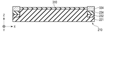
- FIG. 4 is a sectional view showing an outline of a configuration example of the susceptor unit according to the embodiment.
- FIG. 5A is a schematic diagram for explaining the flow of the process gas during the film forming process, and is a diagram showing a case where the height difference between the upper surface of the side guide of the susceptor unit and the upper surface of the wafer is small.
- FIG. 5B is a schematic diagram for explaining the flow of the process gas during the film forming process, and is a diagram showing a case where the height difference between the upper surface of the side guide of the susceptor unit and the upper surface of the wafer is large.
- FIG. 6A is a cross-sectional view showing an outline of a configuration example of a susceptor unit according to an embodiment, and is a view showing a case where a deposit is formed on a side surface guide of the susceptor unit.
- FIG. 6B is a schematic cross-sectional view of a configuration example of the susceptor unit according to the embodiment, and is a diagram showing a case where a deposit is further formed on the side surface guide of the susceptor unit.
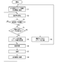
- FIG. 7 is a flowchart showing an outline of an example of a procedure when the film forming process is repeated in the embodiment.
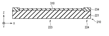
- FIG. 8A is a cross-sectional view schematically showing a configuration example of a susceptor unit according to the first modification.
- FIG. 8B is a cross-sectional view schematically showing a configuration example of the susceptor unit according to the first modification, and is a diagram showing a case where a deposit is formed on the side surface guide of the susceptor unit.
- FIG. 8C is a cross-sectional view schematically showing a configuration example of the susceptor unit according to the first modification, and is a diagram showing a case where a deposit is further formed on the side surface guide of the susceptor unit.
- FIG. 8A is a cross-sectional view schematically showing a configuration example of a susceptor unit according to the first modification.
- FIG. 8B is a cross-sectional view schematically showing a configuration example of the susceptor unit according to the first modification, and
- FIG. 9A is a cross-sectional view showing an outline of a configuration example of a susceptor unit according to the second modification.
- FIG. 9B is a cross-sectional view schematically showing a configuration example of the susceptor unit according to the second modification, and is a diagram showing a case where a deposit is formed on the side surface guide of the susceptor unit.
- FIG. 9C is a cross-sectional view schematically showing a configuration example of the susceptor unit according to the second modification, and is a diagram showing a case where a deposit is further formed on the side surface guide of the susceptor unit.
- FIG. 10A is a sectional view showing a part of the outline of the configuration example of the susceptor unit according to the third modification.
- FIG. 10B is a cross-sectional view showing a part of the outline of the configuration example of the susceptor unit according to the third modified example, and is a view showing a case where a film is deposited on the side surface guide of the susceptor unit.
- FIG. 10C is a cross-sectional view showing a part of the outline of the configuration example of the susceptor unit according to the third modification, and is a diagram showing a case where a deposit is further formed on the side surface guide of the susceptor unit.
- FIG. 11A is a cross-sectional view showing a part of the outline of the configuration example of the susceptor unit according to the fourth modification.
- FIG. 11B is a cross-sectional view showing a part of the outline of the configuration example of the susceptor unit according to the fourth modification, and is a diagram showing a case where a deposit is formed on the side surface guide of the susceptor unit.
- FIG. 11C is a cross-sectional view showing a part of the outline of the configuration example of the susceptor unit according to the fourth modified example, and is a view showing a case where a deposit is further formed on the side surface guide of the susceptor unit.
- the film forming system according to the embodiment will be described with reference to the drawings.
- the film forming system of this embodiment is a system for forming a film by using a CVD method.
- the wafer on which the film is formed is held by the susceptor unit and placed in the film forming chamber. Although a film is formed on the upper surface of the wafer in the film forming chamber, a deposit is also formed on the upper surface of the susceptor unit.
- the film forming system when the film formation on the wafer is completed, the wafer is removed from the susceptor unit. Then, in the film forming system, another wafer is held in the susceptor unit to form a film.
- the deposit on the upper surface of the susceptor unit becomes thick.
- This embodiment is devised so that the deposition conditions on the wafer do not change even if a deposit is formed on the upper surface of the susceptor unit.
- the spacer (adjustment member) provided on the susceptor unit is appropriately changed to a spacer having a different thickness so that the height difference between the upper surface of the wafer and the upper surface of the susceptor unit does not change beyond an allowable value. Can be replaced.
- the technique according to the present embodiment can be used for a film forming process using a CVD method, another vapor phase growth method, or another epitaxial growth method.
- the film forming system 1 includes a preparation chamber 10 and a transfer chamber 20. Further, the film forming system 1 includes a first load lock chamber 30a, a second load lock chamber 30b, a first susceptor replacement chamber 40a, a second susceptor replacement chamber 40b, and a first film formation chamber. 50a and the 2nd film formation chamber 50b are provided. The first load lock chamber 30a and the second load lock chamber 30b are equivalent to each other, the first susceptor exchange chamber 40a and the second susceptor exchange chamber 40b are equivalent to each other, and The film chamber 50a and the second film forming chamber 50b are equivalent.
- the film forming system 1 has two systems of film forming apparatuses for forming a film.
- the film forming system 1 includes a first load lock chamber 30a, a first susceptor replacement chamber 40a, and a first film forming chamber 50a, a first system, a second load lock chamber 30b, and a first load lock chamber 30b.
- the second system includes a second susceptor replacement chamber 40b and a second film formation chamber 50b.
- the first load lock chamber 30a is connected to the preparation chamber 10 via the first gate valve 32a, and is connected to the transfer chamber 20 via the second gate valve 34a.
- the second load lock chamber 30b is connected to the preparation chamber 10 via the third gate valve 32b, and is connected to the transfer chamber 20 via the fourth gate valve 34b. Wafers can be transferred between the preparation chamber 10 and the transfer chamber 20 by the first load lock chamber 30a and the second load lock chamber 30b.
- the first susceptor exchange chamber 40a is connected to the outside via the fifth gate valve 42a, and is also connected to the transfer chamber 20 via the sixth gate valve 44a.
- the second susceptor exchange chamber 40b is connected to the outside via the seventh gate valve 42b, and is connected to the transfer chamber 20 via the eighth gate valve 44b.
- the first susceptor replacement chamber 40a and the second susceptor replacement chamber 40b allow the susceptor unit to be transported between the outside and the transfer chamber 20.
- the first film forming chamber 50a is connected to the transfer chamber 20 via the ninth gate valve 52a.
- the second film forming chamber 50b is connected to the transfer chamber 20 via the tenth gate valve 52b.
- a robot 22 is provided in the transfer chamber 20.
- the robot 22 mounts the wafer or the susceptor unit on which the wafer is placed on the first load lock chamber 30a, the second load lock chamber 30b, the first susceptor replacement chamber 40a, the second susceptor replacement chamber 40b, and the first susceptor replacement chamber 40b.
- the film forming chamber 50a or the second film forming chamber 50b is configured to be transported in and out.
- the preparation room 10 is provided with a robot 12, an aligner 14, a first cassette 16a, and a second cassette 16b.
- a wafer transferred via the first load lock chamber 30a is placed on the first cassette 16a.
- a wafer transferred via the second load lock chamber 30b is placed on the second cassette 16b.
- the wafer is transferred between the preparation chamber 10 and the first load lock chamber 30a and between the preparation chamber 10 and the second load lock chamber 30b.
- a susceptor unit is loaded into the first susceptor replacement chamber 40a from the outside via the fifth gate valve 42a. Similarly, the susceptor unit is loaded into the second susceptor exchange chamber 40b from the outside via the seventh gate valve 42b.
- the robot 22 of the transfer chamber 20 takes out the wafer in the first load lock chamber 30a via the second gate valve 34a and places it on the susceptor unit carried into the first susceptor exchange chamber 40a.
- the robot 22 takes out the susceptor unit in which the wafer in the first susceptor exchange chamber 40a is placed from the first susceptor exchange chamber 40a and places it in the first film formation chamber 50a.
- a CVD method is used to form an epitaxial film of, for example, SiC on the upper surface of the wafer.
- the susceptor unit is composed of carbon, SiC, carbon coated with SiC, carbon coated with TaC, or the like. Further, for the individual parts constituting the susceptor unit, these materials can be individually selected according to the purpose.
- the robot 22 of the transfer chamber 20 takes out the susceptor unit holding the film-formed wafer from the first film-forming chamber 50a and places it in the first susceptor exchange chamber 40a.
- the robot 22 takes out the film-formed wafer from the susceptor unit in the first susceptor exchange chamber 40a and puts it in the first load lock chamber 30a.
- the film-formed wafer in the first load lock chamber 30a is taken out by the robot 12 in the preparation chamber 10 and placed in the first cassette 16a.
- a cassette may be provided in the first load lock chamber 30a and the first susceptor replacement chamber 40a, and a plurality of wafers may be placed in each chamber.
- the film forming system 1 includes a control device 80 that controls the operation of each unit of the film forming system 1.
- the control device 80 includes a CPU (Central Processing Unit) 81, a RAM (Random Access Memory) 82, a ROM (Read Only Memory) 83, a storage 84, an input device 85, which are connected to each other via a bus line.
- a display device 86 and an interface (I/F) 87 are provided.
- the CPU 81 performs various signal processing and the like.
- the operation of the CPU 81 is performed according to the programs and data stored in the RAM 82 and the ROM 83, for example.
- the storage 84 for example, an HDD (Hard Disk Drive), an SSD (Solid State Drive), or the like is used.
- the storage 84 stores various kinds of information such as programs and parameters necessary for executing the functions of the control device 80.
- the programs required for the operation of the control device 80 are loaded from the storage 84 into the RAM 82 and executed by the CPU 81.
- the ROM 83 loads the program from the storage 84 to the RAM 82 when the control device 80 is activated, and thus may store the boot processing program. Any type of device may be used for each device as long as it has an equivalent function.
- the control device 80 is connected to each part of the film forming system 1 via the I/F 87 in order to control each part of the film forming system 1, and inputs and outputs information necessary for the control.
- the X direction and the Y direction are parallel to the upper surface of the wafer to be deposited, and the Z direction (orthogonal to the X direction and the Y direction) are It corresponds to the vertical direction with respect to the upper surface.
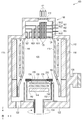
- FIG. 2 is a diagram schematically showing a configuration example of the film forming apparatus 100 provided in the first film forming chamber 50a and the second film forming chamber 50b.
- the film forming apparatus 100 shown in FIG. 2 is a hot wall type thermal CVD apparatus.
- the film forming apparatus 100 is used for forming a SiC epitaxial film, for example.
- the film forming apparatus 100 includes a chamber 112 as a film forming chamber.
- a cylindrical hot wall 116 for example, is provided in the chamber 112, and the inside of the hot wall 116 serves as a film formation region 120 as a reaction chamber.
- the wafer 310 is placed on the susceptor unit 210 below the film formation region 120 in the Z direction.
- Process gas is supplied to the film formation region 120 from a gas supply unit 160 (supply port) provided above in the Z direction.
- the process gas reacts on the upper surface of the wafer 310 held by the susceptor unit 210, and a SiC epitaxial film, for example, is formed by a vapor phase growth reaction.
- the susceptor unit 210 is placed on the rotation holder 150.
- the rotation holder 150 has a cylindrical portion 152 and a rotation shaft 154 fixed to the lower portion of the cylindrical portion 152.
- the cylindrical portion 152 is configured such that the susceptor unit 210 is placed on the upper portion thereof.
- the cylindrical portion 152 has a large opening on the side on which the susceptor unit 210 is placed.
- a motor (not shown) is connected to the rotating shaft 154.
- the rotation holder 150 is configured to rotate by this motor.
- the rotation holder 150 rotates, so that the wafer 310 held by the susceptor unit 210 placed thereon rotates.
- the susceptor unit 210 holding the wafer 310 is transferred to the chamber 112 via the carry-in port 126.
- a bottom heater 132 is provided inside the cylindrical portion 152.
- the bottom heater 132 heats the wafer 310 from its back surface through the opening of the cylindrical portion 152 and the lower portion of the susceptor unit 210.
- the bottom heater 132 includes a disc-shaped in-heater 133 arranged in the center and an annular out-heater 134 arranged on the outer periphery of the in-heater 133.
- a heating heater with electric resistance can be used as the in-heater 133 and the out-heater 134.
- the in-heater 133 and the out-heater 134 can be made of carbon having a predetermined resistance value, SiC, carbon coated with SiC, carbon coated with TaC, or the like.
- the bottom heater 132 is powered by wiring (not shown) provided in the rotating shaft 154.
- the reflector 142 is made of a material having a high heat resistance such as carbon, SiC, carbon coated with SiC, carbon coated with TaC, or the like.
- the reflector 142 may be composed of one plate, or may be composed of a plurality of plates laminated. The reflector 142 contributes to suppressing power consumption of the heater during heating.
- a heat insulating material 144 is provided below the reflector 142 in the Z direction.
- the reflector 142 and the heat insulating material 144 prevent the heat of the bottom heater 132 from being transferred downward in the Z direction of the film forming apparatus 100.
- the hot wall 116 provided laterally in the chamber 112 is made of a highly heat-resistant material such as carbon, SiC, carbon coated with SiC, carbon coated with TaC, or the like.
- a side heater 138 is provided outside the hot wall 116 in the chamber 112. The side heater 138 can also be a heater that uses electrical resistance. The heat generated by the side surface heater 138 heats the film formation region 120, the wafer 310, the susceptor unit 210, and the like via the hot wall 116.
- a heat insulating material 118 is provided between the side heater 138 and the inner wall of the chamber 112. The heat insulating material 118 prevents the heat of the side heater 138 from being transferred to the wall of the chamber 112.
- an exhaust port 122 for exhausting gas is provided.
- the exhaust port 122 is connected to an exhaust mechanism having a regulating valve and a vacuum pump (not shown).
- the inside of the chamber 112 is adjusted to a predetermined pressure via an exhaust mechanism.
- a reflector 124 that reflects radiant heat from the bottom heater 132 and the side heater 138 is provided above the film formation region 120 in the chamber 112 in order to improve thermal efficiency.
- the reflector 124 can be composed of a plate using carbon, SiC, carbon covered with SiC, carbon covered with TaC, or the like.
- the reflector 124 may be configured by one plate or may be configured by stacking a plurality of plates.
- a plurality of gas holes (not shown) may be provided in the reflector 124 to supply the rectifying gas from the upper space of the reflector 124 to the film formation region 120.
- the rectifying gas By supplying the rectifying gas, the convection of the gas in the vicinity of the reflector 124 in the film formation region 120 is suppressed, and the deposition of the deposit on the reflector 124 is suppressed.
- Gas can be introduced into the upper space of the reflector from a gas pipe (not shown). Hydrogen gas, argon gas, or the like is used as the rectifying gas.
- a gas supply unit 160 is provided above the chamber 112.
- the gas supply unit 160 supplies a process gas such as a carrier gas, a source gas, or a doping gas to the film formation region 120.
- the gas supply unit 160 includes, for example, a first gas pipe 1611, a first partition plate 1612, a first gas pipe 161, a second gas pipe 1621, a second partition plate 1622, and a second gas.
- a pipe 162, a third gas pipe 1631, a third partition plate 1632, and a third gas pipe 163 are provided. Gas is supplied from the first gas pipe 161 to the first gas pipe 1611, gas is supplied from the second gas pipe 162 to the second gas pipe 1621, and gas is supplied to the third gas pipe 1631 by the third gas pipe 1631.
- Gas is supplied from the gas pipe 163.
- the partition plates 1612, 1622, 1632 prevent the gases supplied from the gas pipes 161, 162, 163 from being mixed inside the gas supply unit 160.
- the first gas pipe 1611 supplies, for example, hydrogen gas to the deposition region 120.
- the second gas pipe 1621 supplies, for example, a silane gas as a SiC source gas, an HCl gas for improving a growth rate, and a hydrogen gas as a carrier gas thereof to the film formation region 120.
- the third gas pipe 1631 supplies, for example, propane gas as a SiC source gas, nitrogen gas as a doping gas, and hydrogen gas as a carrier gas thereof to the film formation region 120. Note that FIG.
- the actual gas supply unit 160 includes a first gas pipe 1611, a second gas pipe 1621, and a third gas pipe 1631, respectively. It is possible to have a plurality. Further, the arrangement of the first gas pipe 1611, the second gas pipe 1621, and the third gas pipe 1631 is not particularly limited, and any arrangement that can enhance the uniformity such as the film thickness distribution and the carrier concentration distribution can be arbitrarily set. You can choose.
- a radiation thermometer 171 is provided above the gas supply unit 160 for the purpose of measuring the temperature of the wafer 310.
- the radiation thermometer 171 measures the temperature of the wafer 310 through a window 172 made of quartz glass provided on the gas supply unit 160 and a pipe 173.
- the radiation thermometer 171 monitors the temperature at a plurality of points from the central portion of the wafer 310 to the outer peripheral portion.
- the pressure inside the chamber 112 is adjusted to 26.7 kPa, for example.
- the wafer 310 is heated to 1500° C. or higher using the bottom heater 132 and the side heater 138.
- the temperature of the upper surface of the wafer 310 is monitored by using the radiation thermometer 171.
- the temperature is maintained at 1620° C. within ⁇ 1° C.
- the wafer 310 is rotated by the rotation holder 150 at, for example, 600 rpm.
- the SiC epitaxial film is formed on the upper surface of the wafer 310.
- a SiC film having a thickness of, for example, 5 ⁇ m to 10 ⁇ m (hereinafter, the length in the Z direction) is formed over about 30 to 45 minutes.
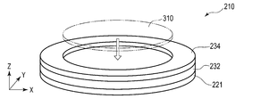
- FIG. 3 is a perspective view showing an outline of a configuration example of the susceptor unit 210.
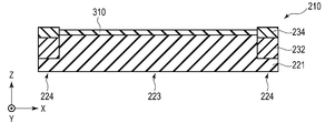
- FIG. 4 is a sectional view showing an outline of a configuration example of the susceptor unit 210.
- the susceptor unit 210 includes at least a back surface support member 221, a spacer 232, and a side surface guide 234.
- the back surface support member 221 is a support member that supports the wafer 310.
- the back surface support member 221 as an example has a substantially disc shape.
- the back surface supporting member 221 has a disk-shaped central portion 223 having a top surface and a bottom surface that are parallel to each other and is flat, and has a diameter substantially the same as that of the wafer 310, and is around the central portion 223 and slightly thinner than the central portion 223. And a peripheral portion 224.
- the spacer 232 as an example has an annular shape.
- the spacer 232 is configured to be placed on the peripheral edge portion 224 of the back surface support member 221. That is, the inner diameter of the spacer 232 is, for example, substantially the same as the diameter of the central portion 223 of the back surface support member 221.
- the outer diameter of the spacer 232 is, for example, substantially the same as the outer diameter of the back surface support member 221.
- the spacer 232 is fitted into the back surface support member 221 so as to surround the central portion 223 of the back surface support member 221.
- the thickness of the spacer 232 is thinner than the difference in thickness between the central portion 223 and the peripheral portion 224 of the back surface support member 221.
- the spacer is an adjusting member for adjusting the position of the upper surface of the side surface guide 234 with respect to the upper surface of the wafer 310, as described later.
- the side guide 234 as an example has an annular shape.
- the side surface guide 234 is configured to be placed on the spacer 232. That is, the inner diameter of the side surface guide 234 is, for example, substantially the same as the diameter of the central portion 223 of the back surface support member 221.
- the outer diameter of the side surface guide 234 is, for example, substantially the same as the outer diameter of the back surface support member 221.
- the side surface guide 234 is fitted into the back surface support member 221 so as to surround the central portion 223 of the back surface support member 221.
- the side surface guide 234 is configured to be provided on the support member so as to surround the outer periphery of the wafer 310 when viewed from the direction (Z direction) perpendicular to the film formation surface of the wafer 310. ..
- the upper surface of the side surface guide 234 is configured to be higher than the central portion 223 of the back surface support member 221. That is, when the spacer 232 and the side surface guide 234 are fitted into the back surface support member 221, a recess is formed on the central portion 223 of the back surface support member 221.
- the wafer 310 is placed in this recess. Since the outer periphery of the wafer 310 is surrounded by the side guides 234, even when the susceptor unit 210 that holds the wafer 310 is rotated by the rotation holder 150 during film formation, the wafer 310 does not shift due to centrifugal force.
- the thickness of the wafer 310 is not limited to this, but is, for example, about 350 ⁇ m.
- the thickness of the spacer 232 is the thickest, and is set to, for example, about 3 mm. Considering the strength, the thickness of the spacer 232 is preferably 300 ⁇ m or more.
- the thickness of the side surface guide 234 is, for example, about 1 mm.
- the diameter of the wafer 310 is, for example, about 100 to 150 mm.
- the width of the annular spacer 232 and the side guide 234 is, for example, about 10 mm.
- the position of the upper surface of the wafer 310 is preferably substantially the same as the position of the upper surface of the side surface guide 234 or slightly higher than the upper surface of the side surface guide 234. ..
- the position of the upper surface of the side guide 234 may be adjusted to be higher than the position of the upper surface of the wafer 310 by, for example, about 150 ⁇ m so that the wafer 310 is not displaced (FIG. 4). That is, the position of the upper surface of the side surface guide 234 with respect to the film formation surface of the wafer 310 is preferably within the above-described predetermined range.
- the back surface support member 221 can be made of, for example, carbon, SiC, carbon coated with SiC, carbon coated with TaC, or the like.
- carbon or carbon coated with TaC is preferably used as the back surface support member 221. This is because SiC or SiC-coated carbon may sublime SiC at a high temperature, and the sublimated SiC may be transferred to the back surface of the wafer 310.
- the side guide 234 can be made of, for example, carbon, SiC, carbon coated with SiC, carbon coated with TaC, or the like.
- the spacer 232 can be made of, for example, carbon, SiC, carbon covered with SiC, carbon covered with TaC, or the like.
- SiC can be used as the side surface guide 234.
- carbon, carbon coated with SiC, and carbon coated with TaC tend to warp during cooling due to the difference in coefficient of thermal expansion with the deposit (SiC) formed on the side surface guide 234.
- carbon or carbon coated with TaC can be used as the spacer 232. This is because one of the SiC and the carbon coated with SiC sublimes between the SiC and the SiC of the side guide 234 and is easily transferred to the other.
- the side guide 234 and the spacer 232 have the same specific heat and the same thermal conductivity.
- the difference between the specific heat of the side surface guide 234 and the specific heat of the spacer 232 is preferably 0.3 J/gK or less, for example.
- the specific heat of SiC varies depending on the manufacturing method, it is approximately 0.65 to 0.67 J/gK, whereas the specific heat of carbon is approximately 0.60 to 0.85 J/gK, which varies depending on the manufacturing method.
- the combination of SiC and carbon is suitable.
- the members that form the susceptor unit 210 need to have heat resistance that can withstand the temperature during the film formation process. Further, it is preferable that the specific heat of the spacer 232 and the specific heat of the material to be deposited are also the same.
- the difference between the specific heat of the spacer 232 and the specific heat of the material to be deposited is preferably 0.3 J/gK or less, for example.
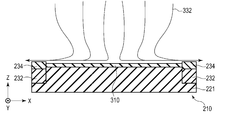
- FIG. 5A is a diagram schematically showing the flow of the process gas 332 on the upper surface of the wafer 310 during film formation.
- the process gas 332 flows from the center toward the outside along the upper surface of the wafer 310.
- the process gas 332 smoothly flows to the outside of the susceptor unit 210 without being disturbed around the side surface guide 234. In this case, the process gas 332 does not stay in the peripheral portion of the wafer 310, and a good film thickness distribution and carrier concentration distribution can be obtained on the upper surface of the wafer 310.
- the film forming process not only the film is formed on the upper surface of the wafer 310, but also the deposit is formed on the upper surface of the side guide 234.
- deposits are successively formed on the upper surface of the side surface guide 234 and become thicker.
- the deposit formed and deposited on the upper surface of the side guide 234 becomes thicker.
- the height difference between the upper surface of the side surface guide 234 on which the deposit 334 is formed and the upper surface of the wafer 310 before the film forming process that is exchanged each time the film forming process is gradually increased.
- this height difference becomes large, turbulence occurs in the flow of the process gas 332.
- the process gas 332 accumulates in the peripheral portion of the wafer 310.
- Such a change in the flow of the process gas 332 may change the film thickness distribution of the film formed on the wafer 310, the carrier concentration distribution, and the like.
- the spacer 232 is replaced with a thinner one, as shown in FIGS. 6A and 6B. In this way, the height difference between the upper surface of the side guide 234 on which the deposit is formed and the upper surface of the wafer 310 is adjusted so as to be within a predetermined range.
- the spacer 232 is replaced.
- the spacer 232 is replaced when the thickness of the deposit 334 increases by 150 ⁇ m, for example, when a film of 10 ⁇ m is formed in one film forming process, the spacer 232 is formed every 15th film forming process. Will be replaced.
- the spacer to be replaced next is a spacer having a thickness of 2850 ⁇ m.
- a plurality of types of spacers 232 having different thicknesses are prepared, and they are exchanged according to the number of film formation processes.
- a spacer set having a plurality of spacers 232 is prepared.
- the back surface support member 221 is composed of one member, but the present invention is not limited to this.
- the back surface support member 221 may be composed of a plurality of members.
- the back surface support member 221 may be configured such that the central portion thereof is lifted up so that the wafer 310 can be easily placed on the susceptor unit 210 and taken out from the susceptor unit 210.
- the lifting central portion and the other portions are configured as separate bodies, and function as the back surface supporting member 221 as a whole.
- 6A and 6B show a mode in which the upper surface of the back surface supporting member 221 is in contact with the back surface of the wafer 310.
- the back surface support member 221 has, for example, a stepped structure on the top surface of the back surface support member 221, so that a space is provided between the top surface of the back surface support member 221 and the back surface of the wafer 310. Good.
- a sequential film formation process for a plurality of wafers 310 using the film formation system 1 according to this embodiment will be described.
- the method described here is a continuous film forming method including replacement of the spacer 232 and the side surface guide 234. All the processes shown here may be fully automatically performed under the control of the control device 80.
- the control device 80 outputs a signal for control to each unit that operates. Further, a part of the processing shown here may be manually performed by the operator.
- the control device 80 may present information on the work to be performed by the operator on the display device 86. That is, the control device 80 outputs data or a signal for displaying the information to the display device 86.
- step S1 the total film thickness of the film deposited on the upper surface of the side surface guide 234 is set to the initial value.
- the total film thickness is set to 0 ⁇ m.
- a predetermined value is cumulatively added to the total film thickness every time the film forming process is performed until the total film thickness is reset to the initial value (step S9 ⁇ step S1). ..
- a deposit having a thickness approximately equal to the film thickness of a predetermined film thickness formed on the wafer 310 is formed on the upper surface of the side surface guide 234 by one film forming process on the wafer 310.
- the design value is used as the predetermined value added to the total film thickness. That is, since the film thickness formed on the wafer 310 by one film formation process on the wafer 310 is known as a design value, the total film thickness is calculated by repeating the film formation process every time the film formation process is repeated. (Film thickness) is added.
- the film formed on the wafer 310 and the thickness formed on the upper surface of the side surface guide 234 are significantly different from each other by one film formation process on the wafer 310, the film formed on the wafer 310.
- the total film thickness can be set by correlating the thickness with the film thickness of the deposit formed on the upper surface of the side surface guide 234.
- step S1 the spacer type indicator indicating which spacer is used among the plurality of spacers having different thicknesses is also set to the type of spacer used first.
- the new side guide 234 is used and the thickest spacer 232 is used, it is set to the indicator that indicates the thickest spacer.
- another spacer 232 is used, it is set to an indicator corresponding to that type of spacer.
- the information of the total film thickness and the indicator of the spacer type is stored in, for example, the RAM 82 or the storage 84 and used for processing. These pieces of information stored in the RAM 82 or the storage 84 can be updated by the processing of steps S5, S8, and S9 described below.
- step S2 the upper surface of the side guide 234 on which the deposit 334 is formed (the upper surface of the side guide 234 in the initial state because there is no deposit 334) and the film formation surface based on the current value of the total film thickness.
- the height difference from the upper surface of the wafer 310 is calculated.
- the position of the upper surface of the side surface guide 234 is obtained based on the total film thickness since the thickness of the spacer 232 corresponding to the type of the spacer 232 used and the thickness of the side surface guide 234 are known.
- the position of the upper surface of the wafer 310 is also determined by the known thickness of the wafer 310.
- step S3 it is determined whether or not the height difference calculated in step S2 is larger than the allowable value.
- the film forming process can be performed. Therefore, the process proceeds to S6, where the film forming preparation is performed and the film forming process is executed as described later.
- the allowable value is stored in the RAM 82 or the storage 84, for example, and can be set appropriately.
- step S3 When it is determined in step S3 that the height difference is larger than the allowable value, the process proceeds to step S4.
- step S4 it is determined whether there is a replaceable spacer. Replaceable spacers are spacers that are thinner than the spacers currently in use. When it is determined in step S4 that there is a replaceable spacer, the process proceeds to step S5.
- the spacer 232 is replaced in step S5. That is, in the susceptor replacement chamber, the side guide 234 and the spacer 232 are removed from the back surface supporting member 221, and a thinner spacer is placed instead of the spacer that has been used until then and the spacer that has been used is removed. The side guide 234 is placed. At this time, the stored indicator showing the type of spacer in use is changed to the indicator showing the type of spacer after replacement.
- the replacement of the spacer 232 may be performed manually by an operator, or a dedicated device may be provided. Thereafter, the process proceeds to step S6. That is, as shown below, the film formation preparation is performed and the film formation process is executed.
- step S6 film forming preparations such as transfer of the wafer 310 and the susceptor unit 210 into the chamber 112 and adjustment of the temperature in the chamber 112 are performed.
- step S7 a film forming process is executed. That is, the susceptor unit 210 is rotated using the rotation holder 150 in the chamber 112 heated to an appropriate temperature. In this state, the process gas is supplied, and a film such as a SiC crystal film is formed on the wafer 310. At the same time, a deposit of SiC, for example, is also formed on the upper surface of the side guide 234.
- step S8 for example, the total film thickness is formed on the wafer 310 by the film forming process of step S7. Formed on the upper surface of the side surface guide 234, which is obtained from the relationship between the film thickness of the deposited film formed on the upper surface of the side surface guide 234 and the film thickness of the film formed on the wafer 310 which has been examined in advance. The thickness of the deposited deposit is added. The stored total film thickness is updated to a value indicating the film thickness of the deposit on the side surface guide 234 after the film forming process. That is, the total film thickness is updated based on the film thickness formed on the wafer 310. After that, the process returns to step S2 to calculate the height difference and determine whether the next film formation is allowed.
- step S9 the side surface guide 234 and the spacer 232 are exchanged. That is, in the spacer exchange chamber, the side guides 234 and the spacers 232 which have been used until now are removed from the back surface supporting member 221, and instead, the thickest spacers 232 are placed and the deposit 334 is formed thereon. A new or cleaned side guide 234 is placed. The spacers used so far can be used repeatedly. Then, the process proceeds to step S1.
- the stored total film thickness is reset to 0 ⁇ m, and the indicator corresponding to the type of the thickest spacer is set to the stored indicator indicating the type of spacer in use.
- the subsequent processing is the same as described above. These procedures are repeated while the series of film forming processes are repeated, and are ended when the series of film forming processes is completed.
- the height difference between the upper surface of the side guide 234 (the upper surface of the deposit 334) and the upper surface of the wafer 310 falls within a predetermined range by replacing the spacer 232. Therefore, in the film forming process, the flow of the process gas on the upper surface of the wafer 310 does not change even if the film forming process is repeated, which influences the film thickness and the properties of the film to be formed.
- the specific heat of the spacer 232, the side guide 234, and the deposit 334 is almost the same. Further, even if the thickness of the deposit 334 is increased, the total volume of the spacer 232, the side surface guide 234, and the deposit 334 is within the allowable range. Therefore, the heat capacity of the spacer 232, the side guides 234, and the deposit 334 together becomes constant within an allowable range even if the deposit 334 becomes thick. That is, the temperature of the outer peripheral portion of the wafer 310 can be kept constant within an allowable range.
- the position of the upper surface of the wafer 310, which is the target of the film formation process, in the chamber 112 does not change during the repeated film formation processes. Further, the form in which the wafer 310 is placed on the susceptor unit 210 does not change. From the above, even if the deposit 334 becomes thicker or the spacer 232 is replaced, the film forming conditions can be made constant through repeated film forming processes. As a result, the film formed on the wafer 310 also becomes uniform.
- the position of the wafer 310 that is the target of the film formation process in the chamber 112 does not change during the repeated film formation processes. That is, even if the film forming process is repeated, the position of the upper surface of the wafer 310 to be film formed does not change with respect to the other components of the chamber 112. This means that it becomes easy to stably obtain information for grasping the state of the film forming process, such as temperature measurement by the radiation thermometer 171. This point also contributes to making the film formed on the wafer 310 uniform.
- the present embodiment is particularly effective when a SiC film is formed. It is possible to remove the deposit by performing a cleaning process on the side guide 234 on which the deposit 334 is formed.
- the cleaning process is a process of removing deposits formed on the side surface guide 234 by a chemical process or a process of mechanically scraping.
- the composition of the deposit 334 formed on the upper surface of the side guide 234 is Si or GaN
- a cleaning method using such a gas has not been established.
- the side guide 234 on which the SiC deposit is formed needs to remove the SiC deposit by, for example, polishing. Mechanical cleaning is time-consuming and may damage the side guides 234. Further, even in the case of the chemical treatment, for example, when the composition of the deposit is SiC and the side guide 234 is also made of SiC, a part of the side guide is removed together with the removal of the deposit (over). Etching). That is, it is difficult to remove only the SiC deposits formed on the upper surface of the side surface guide 234, and even if it is possible, it is expensive.
- the film thickness formed on the wafer 310 in a single film forming process is generally relatively thick, such as 5 ⁇ m or more.
- the film thickness of the deposit 334 on the side guide 234 that does not affect the film thickness distribution of the film formed on the wafer 310 is limited to about 150 to 500 ⁇ m. Therefore, since the limit is reached with a small number of film forming processes, the height difference between the upper surface of the side surface guide 234 and the upper surface of the wafer 310 as described with reference to FIG. 5B is likely to be a problem. Therefore, if no measures are taken, the side guide 234 will be replaced more frequently, and its cost will be a problem.
- the above problems can be solved without providing a special mechanism such as a lifting mechanism using a motor in the susceptor unit 210 or the film forming apparatus 100.
- the positional relationship between the susceptor unit 210 and the constituent elements of the film forming apparatus 100 such as the heater, the gas supply unit 160, the radiation thermometer 171 and the like does not change. Therefore, while maintaining the setting conditions of the film forming apparatus 100 for the wafer 310, the above problem can be solved by a simple method of replacing the spacer 232.
- the bottom heater 132 is provided below the susceptor unit 210, and heating is performed from below the susceptor unit 210.
- the lower portion of the susceptor unit 210 does not change.
- the positional relationship between the back surface supporting member 221 and the out heater 134 or the positional relationship between the back surface supporting member 221 and the wafer 310 does not change. Therefore, various conditions do not change during the repetition of the film forming process, and the effect that the adjustment of the film forming condition becomes unnecessary or easy is obtained.
- a plurality of spacers having different thicknesses are prepared as the spacer 232, and the spacer to be used is selected according to the film thickness of the deposit 334 formed. However, it is not limited to this. Whether to insert the spacer 232 may be selected depending on the film thickness of the deposit 334. Further, the number of the spacers 232 simultaneously inserted into the susceptor unit 210 is not limited to one. A plurality of spacers 232 may be inserted, and the thickness may be adjusted depending on the number of spacers 232. However, if the spacer 232 has a certain thickness, it is easier to handle and has higher durability. Therefore, when a plurality of spacers 232 are used, the thickness of the spacer 232 should be determined in consideration of ease of handling. In either case, the spacer 232 is selectively inserted depending on the thickness of the deposit.
- FIGS. 8A, 8B, and 8C A schematic diagram of this modification is shown in FIGS. 8A, 8B, and 8C.
- FIG. 8A when there is no deposit on the side surface guide 234, the wafer 310 is placed on the back surface supporting member 221.
- FIG. 8B when a deposit 334 is formed on the side surface guide 234, a spacer 242 having a thickness corresponding to the thickness of the deposit 334 is placed on the back surface supporting member 221, and a wafer is placed on the spacer 242. 310 is placed.
- FIG. 8C when the deposit 334 becomes thicker, the spacer 242 is replaced with a thicker one accordingly.
- the shape of the spacer 242 may not support the entire back surface of the wafer 310, such as a ring shape.
- the height difference between the upper surface of the deposit 334 on the side surface guide 234 and the upper surface of the wafer 310 is within a predetermined range. Therefore, similar to the above-described embodiment, the flow of the process gas on the upper surface of the wafer 310 does not undergo unacceptable changes such as disturbances through the repeated film forming processes. Therefore, the film formed on the wafer 310 is uniform.
- the back surface support member 221 may be replaced. That is, as shown in FIGS. 9A, 9B, and 9C, depending on the film thickness of the deposit 334 on the side surface guide 234, the central portion 223 or the peripheral edge portion 224, or both the central portion 223 and the peripheral edge portion 224 may be formed.
- An appropriate back surface support member 221 may be selected from a plurality of back surface support members 221 having different film thicknesses. The back surface support member 221 does not have to have a structure that supports the entire back surface of the wafer 310.
- the height difference between the upper surface of the side surface guide 234 and the upper surface of the wafer 310 is within a predetermined range. Therefore, the flow of the process gas on the upper surface of the wafer 310 does not undergo unacceptable changes such as turbulence during the repeated film forming processes. Furthermore, the back surface supporting member 221, the side surface guide 234, and the deposit 334 are adjusted so that their combined sizes are almost the same, so that their heat capacities, the position of the upper surface of the wafer 310, and the configuration of the back surface side of the wafer 310 are adjusted. Does not change. As a result, it is not necessary to change the setting conditions of the film forming apparatus 100 for the wafer 310, and the film formed on the wafer 310 becomes uniform.
- the number of parts can be reduced by not using spacers.
- the spacer by using the spacer, the back surface support member 221 can be shared.
- the first modified example, and the second modified example may be used in combination. That is, the spacer 232 inserted between the back surface support member 221 and the side surface guide 234 and the spacer 242 inserted between the back surface support member 221 and the wafer 310 are used at the same time, or the back surface support member 221 is It may be exchanged.
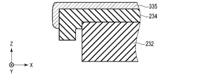
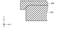
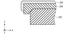
- the reaction product of the process gas may adhere not only to the upper surface of the side surface guide 234 but also to the side surface of the side surface guide 234 and the spacer 232. Furthermore, the reaction product may also enter between the spacer 232 and the side guide 234 due to processing variations between the spacer 232 and the side guide 234. When the reaction product enters between the side surface guide 234 and the spacer 232 and the reaction product adheres to one of the side surface guide 234 and the spacer 232, the adhesion between the spacer 232 and the side surface guide 234 gradually deteriorates. Therefore, the side guide 234 may partially float from the spacer 232.
- Such a state causes rattling between the side guides 234 and the spacers 232, which adversely affects the stability when the rotary holder 150 rotates at high speed. Further, the contact areas of the side guides 234 and the spacers 232 are different, which makes it difficult to keep the temperature of the outer peripheral portion of the wafer 310 constant within an allowable range.
- the shape of the peripheral edge portion of the side surface guide 234 may be a shape that covers the spacer 232.
- the reaction product 335 is less likely to enter the interface between the side surface guide 234 and the spacer 232 as shown in FIGS. 10B and 10C.
- the spacer 232 and the side surface guide 234 may be configured so that the outer diameter of the spacer 232 can be changed.
- the peripheral edge of the side surface guide 234 is shaped so as to cover the spacer 232.
- the outer diameter of the spacer 232 is not changed when the reaction product 335 does not go around under the outer periphery of the side surface guide 234.
- FIG. 11C when the adhesion of the reaction product 335 further increases and goes around to the lower side of the outer periphery of the side surface guide 234, the spacer 232 is replaced with a spacer having a smaller outer diameter.
- the spacer 232 and the side guide 234 may be configured so that the attached reaction product 335 does not affect the interface between the side guide 234 and the spacer 232. ..
- a gap may be provided between the side surface of the wafer 310 and the inner side surface of the side surface guide 234 in consideration of processing variations, thermal expansion, transfer accuracy of the wafer 310, and the like. Further, a gap may be provided between the inner side surfaces of the spacer 232 and the side surface guide 234 and the side surface of the central portion 223 of the back surface support member 221 in consideration of processing variations and thermal expansion.
- the deposit 334 is formed not only on the upper surface of the side surface guide 234 but also on the inner side surface of the side surface guide 234, and it may protrude in the inner circumferential direction of the side surface guide 234.
- the wafer 310 may interfere with the wafer 310, and the wafer 310 may not be removable from the susceptor unit 210. Therefore, as the allowable value of the height difference shown in step S3 of FIG. 7, it is possible to determine not only the height difference but also the amount of protrusion.
- the amount of protrusion can be reflected in the allowable value in step S3 of FIG. 7 by obtaining the relationship with the film thickness formed on the wafer 310 in advance.
- a protruding portion of the deposit 334 can be removed in a short time by a simple grinding device. Therefore, between the steps S3 and S4, the side surface guide 234 is temporarily taken out and deposited. A step of grinding the protruding portion of the object 334 may be added.
Landscapes
- Chemical & Material Sciences (AREA)
- Chemical Kinetics & Catalysis (AREA)
- General Chemical & Material Sciences (AREA)
- Engineering & Computer Science (AREA)
- Materials Engineering (AREA)
- Mechanical Engineering (AREA)
- Metallurgy (AREA)
- Organic Chemistry (AREA)
- Inorganic Chemistry (AREA)
- Chemical Vapour Deposition (AREA)
Abstract
La présente invention porte sur un procédé de formation de film consistant : à placer une tranche sur une unité suscepteur dotée d'un élément de support servant au montage de la tranche, d'un guide de surface latérale qui est disposé sur l'élément de support et qui entoure au moins une partie de la circonférence externe de la tranche, et d'une entretoise servant à régler la position de la surface supérieure de la tranche et de la surface supérieure du guide de surface latérale ; à former un film prescrit sur la surface supérieure de la tranche montée et à former un film sur le guide de surface latérale ; à régler, à l'aide de l'entretoise et en fonction de l'épaisseur du film prescrit qui a été formé, la position de la surface supérieure du guide de surface latérale par rapport à la surface supérieure de la tranche ; et à monter une nouvelle tranche sur l'unité suscepteur à position réglée et à former un nouveau film prescrit.
Priority Applications (4)
| Application Number | Priority Date | Filing Date | Title |
|---|---|---|---|
| CN201980078629.9A CN113169051A (zh) | 2018-12-07 | 2019-12-06 | 成膜方法、成膜装置、基座单元以及基座单元所使用的间隔件组 |
| KR1020217016696A KR20210072116A (ko) | 2018-12-07 | 2019-12-06 | 성막 방법, 성막 장치, 서셉터 유닛, 및 서셉터 유닛에 사용되는 스페이서 세트 |
| EP19891990.4A EP3893268A4 (fr) | 2018-12-07 | 2019-12-06 | Procédé et dispositif de formation de film, unité suscepteur, et ensemble entretoise utilisé dans une unité suscepteur |
| US17/340,161 US20210292897A1 (en) | 2018-12-07 | 2021-06-07 | Deposition method, deposition apparatus, susceptor unit, and spacer set used in susceptor unit |
Applications Claiming Priority (2)
| Application Number | Priority Date | Filing Date | Title |
|---|---|---|---|
| JP2018-229825 | 2018-12-07 | ||
| JP2018229825A JP7023826B2 (ja) | 2018-12-07 | 2018-12-07 | 連続成膜方法、連続成膜装置、サセプタユニット、及びサセプタユニットに用いられるスペーサセット |
Related Child Applications (1)
| Application Number | Title | Priority Date | Filing Date |
|---|---|---|---|
| US17/340,161 Continuation US20210292897A1 (en) | 2018-12-07 | 2021-06-07 | Deposition method, deposition apparatus, susceptor unit, and spacer set used in susceptor unit |
Publications (1)
| Publication Number | Publication Date |
|---|---|
| WO2020116618A1 true WO2020116618A1 (fr) | 2020-06-11 |
Family
ID=70973487
Family Applications (1)
| Application Number | Title | Priority Date | Filing Date |
|---|---|---|---|
| PCT/JP2019/047840 Ceased WO2020116618A1 (fr) | 2018-12-07 | 2019-12-06 | Procédé et dispositif de formation de film, unité suscepteur, et ensemble entretoise utilisé dans une unité suscepteur |
Country Status (7)
| Country | Link |
|---|---|
| US (1) | US20210292897A1 (fr) |
| EP (1) | EP3893268A4 (fr) |
| JP (1) | JP7023826B2 (fr) |
| KR (1) | KR20210072116A (fr) |
| CN (1) | CN113169051A (fr) |
| TW (1) | TWI734286B (fr) |
| WO (1) | WO2020116618A1 (fr) |
Families Citing this family (3)
| Publication number | Priority date | Publication date | Assignee | Title |
|---|---|---|---|---|
| WO2022205480A1 (fr) * | 2021-04-02 | 2022-10-06 | 眉山博雅新材料有限公司 | Procédé de préparation de cristal composite, et système |
| US12538756B2 (en) * | 2022-05-06 | 2026-01-27 | Nuflare Technology, Inc. | Vapor phase growth apparatus and reflector |
| JP2026013515A (ja) | 2024-07-17 | 2026-01-29 | 東京エレクトロン株式会社 | 成膜装置及びその整備方法 |
Citations (7)
| Publication number | Priority date | Publication date | Assignee | Title |
|---|---|---|---|---|
| JP2001274104A (ja) * | 1999-12-10 | 2001-10-05 | Applied Materials Inc | 自己整列の非接触シャドーリング処理キット |
| JP2005277369A (ja) * | 2003-09-05 | 2005-10-06 | Tokyo Electron Ltd | フォーカスリング及びプラズマ処理装置 |
| JP2006319043A (ja) * | 2005-05-11 | 2006-11-24 | Hitachi High-Technologies Corp | プラズマ処理装置 |
| JP2007180153A (ja) | 2005-12-27 | 2007-07-12 | Hitachi Cable Ltd | 化合物半導体の製造方法及び装置 |
| JP2008244274A (ja) * | 2007-03-28 | 2008-10-09 | Tokyo Electron Ltd | プラズマ処理装置 |
| JP2011258859A (ja) * | 2010-06-11 | 2011-12-22 | Toshiba Corp | 薄膜形成装置 |
| JP2017228708A (ja) * | 2016-06-24 | 2017-12-28 | 東京エレクトロン株式会社 | プラズマ成膜装置および基板載置台 |
Family Cites Families (11)
| Publication number | Priority date | Publication date | Assignee | Title |
|---|---|---|---|---|
| US6113702A (en) * | 1995-09-01 | 2000-09-05 | Asm America, Inc. | Wafer support system |
| US7252738B2 (en) * | 2002-09-20 | 2007-08-07 | Lam Research Corporation | Apparatus for reducing polymer deposition on a substrate and substrate support |
| WO2012092064A1 (fr) * | 2010-12-30 | 2012-07-05 | Veeco Instruments Inc. | Traitement de plaquette avec extension de vecteur |
| US10034330B2 (en) * | 2013-03-15 | 2018-07-24 | National Oilwell Varco, L.P. | System and method for heat treating a tubular |
| US8940614B2 (en) * | 2013-03-15 | 2015-01-27 | Dow Corning Corporation | SiC substrate with SiC epitaxial film |
| CN107004583B (zh) * | 2014-12-02 | 2020-06-26 | 昭和电工株式会社 | 晶片支承台、化学气相生长装置、外延晶片及其制造方法 |
| US10648079B2 (en) * | 2014-12-19 | 2020-05-12 | Lam Research Corporation | Reducing backside deposition at wafer edge |
| CN108369922B (zh) * | 2016-01-26 | 2023-03-21 | 应用材料公司 | 晶片边缘环升降解决方案 |
| JP6796431B2 (ja) * | 2016-08-12 | 2020-12-09 | 東京エレクトロン株式会社 | 成膜装置、およびそれに用いるガス吐出部材 |
| KR102723647B1 (ko) * | 2016-10-12 | 2024-10-29 | 램 리써치 코포레이션 | 반도체 프로세싱용 웨이퍼 포지셔닝 페데스탈의 패드 상승 메커니즘 |
| US10655224B2 (en) * | 2016-12-20 | 2020-05-19 | Lam Research Corporation | Conical wafer centering and holding device for semiconductor processing |
-
2018
- 2018-12-07 JP JP2018229825A patent/JP7023826B2/ja active Active
-
2019
- 2019-12-05 TW TW108144420A patent/TWI734286B/zh active
- 2019-12-06 EP EP19891990.4A patent/EP3893268A4/fr not_active Withdrawn
- 2019-12-06 WO PCT/JP2019/047840 patent/WO2020116618A1/fr not_active Ceased
- 2019-12-06 CN CN201980078629.9A patent/CN113169051A/zh active Pending
- 2019-12-06 KR KR1020217016696A patent/KR20210072116A/ko not_active Ceased
-
2021
- 2021-06-07 US US17/340,161 patent/US20210292897A1/en not_active Abandoned
Patent Citations (7)
| Publication number | Priority date | Publication date | Assignee | Title |
|---|---|---|---|---|
| JP2001274104A (ja) * | 1999-12-10 | 2001-10-05 | Applied Materials Inc | 自己整列の非接触シャドーリング処理キット |
| JP2005277369A (ja) * | 2003-09-05 | 2005-10-06 | Tokyo Electron Ltd | フォーカスリング及びプラズマ処理装置 |
| JP2006319043A (ja) * | 2005-05-11 | 2006-11-24 | Hitachi High-Technologies Corp | プラズマ処理装置 |
| JP2007180153A (ja) | 2005-12-27 | 2007-07-12 | Hitachi Cable Ltd | 化合物半導体の製造方法及び装置 |
| JP2008244274A (ja) * | 2007-03-28 | 2008-10-09 | Tokyo Electron Ltd | プラズマ処理装置 |
| JP2011258859A (ja) * | 2010-06-11 | 2011-12-22 | Toshiba Corp | 薄膜形成装置 |
| JP2017228708A (ja) * | 2016-06-24 | 2017-12-28 | 東京エレクトロン株式会社 | プラズマ成膜装置および基板載置台 |
Also Published As
| Publication number | Publication date |
|---|---|
| CN113169051A (zh) | 2021-07-23 |
| US20210292897A1 (en) | 2021-09-23 |
| EP3893268A4 (fr) | 2022-08-24 |
| JP2020092227A (ja) | 2020-06-11 |
| JP7023826B2 (ja) | 2022-02-22 |
| EP3893268A1 (fr) | 2021-10-13 |
| TW202029295A (zh) | 2020-08-01 |
| KR20210072116A (ko) | 2021-06-16 |
| TWI734286B (zh) | 2021-07-21 |
Similar Documents
| Publication | Publication Date | Title |
|---|---|---|
| JP5732284B2 (ja) | 成膜装置および成膜方法 | |
| TWI404819B (zh) | 成膜裝置及成膜方法 | |
| JP5851149B2 (ja) | 成膜装置および成膜方法 | |
| WO2012092127A1 (fr) | Procédés et systèmes d'étalonnage in-situ de pyromètre | |
| JP6444641B2 (ja) | 成膜装置、サセプタ、及び成膜方法 | |
| WO2011114858A1 (fr) | Procédé de fabrication de couche mince semi-conductrice, appareil de fabrication de couche mince semi-conductrice, suscepteur, et porte-suscepteur | |
| EP2741316B1 (fr) | Dispositif de fabrication de tranche épitaxiale et procédé de fabrication | |
| US20210292897A1 (en) | Deposition method, deposition apparatus, susceptor unit, and spacer set used in susceptor unit | |
| JP5204721B2 (ja) | 成膜装置および成膜方法 | |
| CN111033692A (zh) | 气相生长方法 | |
| JP5988486B2 (ja) | 成膜装置および成膜方法 | |
| US12065732B2 (en) | Film forming method and film forming apparatus | |
| KR102581343B1 (ko) | 성막 장치 | |
| JP2020191346A (ja) | サセプタおよびエピタキシャル成長装置 | |
| JP7435266B2 (ja) | サセプタ、化学気相成長装置及びエピタキシャルウェハの製造方法 | |
| JPH0997765A (ja) | 基板処理装置 | |
| JP2012175020A (ja) | 基板処理装置 | |
| JPWO2003003432A1 (ja) | 気相成長方法および気相成長装置 | |
| JP5736291B2 (ja) | 成膜装置および成膜方法 | |
| JP7701895B2 (ja) | サセプタ及びその製造方法 | |
| HK40027052A (zh) | 气相生长方法 | |
| JP2018181932A (ja) | 気相成長装置及びサセプタの管理方法 |
Legal Events
| Date | Code | Title | Description |
|---|---|---|---|
| 121 | Ep: the epo has been informed by wipo that ep was designated in this application |
Ref document number: 19891990 Country of ref document: EP Kind code of ref document: A1 |
|
| ENP | Entry into the national phase |
Ref document number: 20217016696 Country of ref document: KR Kind code of ref document: A |
|
| NENP | Non-entry into the national phase |
Ref country code: DE |
|
| ENP | Entry into the national phase |
Ref document number: 2019891990 Country of ref document: EP Effective date: 20210707 |