WO2020116618A1 - 成膜方法、成膜装置、サセプタユニット、及びサセプタユニットに用いられるスペーサセット - Google Patents
成膜方法、成膜装置、サセプタユニット、及びサセプタユニットに用いられるスペーサセット Download PDFInfo
- Publication number
- WO2020116618A1 WO2020116618A1 PCT/JP2019/047840 JP2019047840W WO2020116618A1 WO 2020116618 A1 WO2020116618 A1 WO 2020116618A1 JP 2019047840 W JP2019047840 W JP 2019047840W WO 2020116618 A1 WO2020116618 A1 WO 2020116618A1
- Authority
- WO
- WIPO (PCT)
- Prior art keywords
- wafer
- film
- spacer
- film forming
- guide
- Prior art date
- Legal status (The legal status is an assumption and is not a legal conclusion. Google has not performed a legal analysis and makes no representation as to the accuracy of the status listed.)
- Ceased
Links
Images









Classifications
-
- C—CHEMISTRY; METALLURGY
- C23—COATING METALLIC MATERIAL; COATING MATERIAL WITH METALLIC MATERIAL; CHEMICAL SURFACE TREATMENT; DIFFUSION TREATMENT OF METALLIC MATERIAL; COATING BY VACUUM EVAPORATION, BY SPUTTERING, BY ION IMPLANTATION OR BY CHEMICAL VAPOUR DEPOSITION, IN GENERAL; INHIBITING CORROSION OF METALLIC MATERIAL OR INCRUSTATION IN GENERAL
- C23C—COATING METALLIC MATERIAL; COATING MATERIAL WITH METALLIC MATERIAL; SURFACE TREATMENT OF METALLIC MATERIAL BY DIFFUSION INTO THE SURFACE, BY CHEMICAL CONVERSION OR SUBSTITUTION; COATING BY VACUUM EVAPORATION, BY SPUTTERING, BY ION IMPLANTATION OR BY CHEMICAL VAPOUR DEPOSITION, IN GENERAL
- C23C16/00—Chemical coating by decomposition of gaseous compounds, without leaving reaction products of surface material in the coating, i.e. chemical vapour deposition [CVD] processes
- C23C16/44—Chemical coating by decomposition of gaseous compounds, without leaving reaction products of surface material in the coating, i.e. chemical vapour deposition [CVD] processes characterised by the method of coating
- C23C16/458—Chemical coating by decomposition of gaseous compounds, without leaving reaction products of surface material in the coating, i.e. chemical vapour deposition [CVD] processes characterised by the method of coating characterised by the method used for supporting substrates in the reaction chamber
- C23C16/4582—Rigid and flat substrates, e.g. plates or discs
- C23C16/4583—Rigid and flat substrates, e.g. plates or discs the substrate being supported substantially horizontally
- C23C16/4585—Devices at or outside the perimeter of the substrate support, e.g. clamping rings, shrouds
-
- H—ELECTRICITY
- H10—SEMICONDUCTOR DEVICES; ELECTRIC SOLID-STATE DEVICES NOT OTHERWISE PROVIDED FOR
- H10P—GENERIC PROCESSES OR APPARATUS FOR THE MANUFACTURE OR TREATMENT OF DEVICES COVERED BY CLASS H10
- H10P14/00—Formation of materials, e.g. in the shape of layers or pillars
- H10P14/60—Formation of materials, e.g. in the shape of layers or pillars of insulating materials
- H10P14/63—Formation of materials, e.g. in the shape of layers or pillars of insulating materials characterised by the formation processes
- H10P14/6326—Deposition processes
- H10P14/6328—Deposition from the gas or vapour phase
- H10P14/6334—Deposition from the gas or vapour phase using decomposition or reaction of gaseous or vapour phase compounds, i.e. chemical vapour deposition
-
- C—CHEMISTRY; METALLURGY
- C23—COATING METALLIC MATERIAL; COATING MATERIAL WITH METALLIC MATERIAL; CHEMICAL SURFACE TREATMENT; DIFFUSION TREATMENT OF METALLIC MATERIAL; COATING BY VACUUM EVAPORATION, BY SPUTTERING, BY ION IMPLANTATION OR BY CHEMICAL VAPOUR DEPOSITION, IN GENERAL; INHIBITING CORROSION OF METALLIC MATERIAL OR INCRUSTATION IN GENERAL
- C23C—COATING METALLIC MATERIAL; COATING MATERIAL WITH METALLIC MATERIAL; SURFACE TREATMENT OF METALLIC MATERIAL BY DIFFUSION INTO THE SURFACE, BY CHEMICAL CONVERSION OR SUBSTITUTION; COATING BY VACUUM EVAPORATION, BY SPUTTERING, BY ION IMPLANTATION OR BY CHEMICAL VAPOUR DEPOSITION, IN GENERAL
- C23C16/00—Chemical coating by decomposition of gaseous compounds, without leaving reaction products of surface material in the coating, i.e. chemical vapour deposition [CVD] processes
- C23C16/22—Chemical coating by decomposition of gaseous compounds, without leaving reaction products of surface material in the coating, i.e. chemical vapour deposition [CVD] processes characterised by the deposition of inorganic material, other than metallic material
- C23C16/30—Deposition of compounds, mixtures or solid solutions, e.g. borides, carbides, nitrides
- C23C16/32—Carbides
- C23C16/325—Silicon carbide
-
- C—CHEMISTRY; METALLURGY
- C23—COATING METALLIC MATERIAL; COATING MATERIAL WITH METALLIC MATERIAL; CHEMICAL SURFACE TREATMENT; DIFFUSION TREATMENT OF METALLIC MATERIAL; COATING BY VACUUM EVAPORATION, BY SPUTTERING, BY ION IMPLANTATION OR BY CHEMICAL VAPOUR DEPOSITION, IN GENERAL; INHIBITING CORROSION OF METALLIC MATERIAL OR INCRUSTATION IN GENERAL
- C23C—COATING METALLIC MATERIAL; COATING MATERIAL WITH METALLIC MATERIAL; SURFACE TREATMENT OF METALLIC MATERIAL BY DIFFUSION INTO THE SURFACE, BY CHEMICAL CONVERSION OR SUBSTITUTION; COATING BY VACUUM EVAPORATION, BY SPUTTERING, BY ION IMPLANTATION OR BY CHEMICAL VAPOUR DEPOSITION, IN GENERAL
- C23C16/00—Chemical coating by decomposition of gaseous compounds, without leaving reaction products of surface material in the coating, i.e. chemical vapour deposition [CVD] processes
- C23C16/44—Chemical coating by decomposition of gaseous compounds, without leaving reaction products of surface material in the coating, i.e. chemical vapour deposition [CVD] processes characterised by the method of coating
- C23C16/458—Chemical coating by decomposition of gaseous compounds, without leaving reaction products of surface material in the coating, i.e. chemical vapour deposition [CVD] processes characterised by the method of coating characterised by the method used for supporting substrates in the reaction chamber
- C23C16/4581—Chemical coating by decomposition of gaseous compounds, without leaving reaction products of surface material in the coating, i.e. chemical vapour deposition [CVD] processes characterised by the method of coating characterised by the method used for supporting substrates in the reaction chamber characterised by material of construction or surface finish of the means for supporting the substrate
-
- C—CHEMISTRY; METALLURGY
- C23—COATING METALLIC MATERIAL; COATING MATERIAL WITH METALLIC MATERIAL; CHEMICAL SURFACE TREATMENT; DIFFUSION TREATMENT OF METALLIC MATERIAL; COATING BY VACUUM EVAPORATION, BY SPUTTERING, BY ION IMPLANTATION OR BY CHEMICAL VAPOUR DEPOSITION, IN GENERAL; INHIBITING CORROSION OF METALLIC MATERIAL OR INCRUSTATION IN GENERAL
- C23C—COATING METALLIC MATERIAL; COATING MATERIAL WITH METALLIC MATERIAL; SURFACE TREATMENT OF METALLIC MATERIAL BY DIFFUSION INTO THE SURFACE, BY CHEMICAL CONVERSION OR SUBSTITUTION; COATING BY VACUUM EVAPORATION, BY SPUTTERING, BY ION IMPLANTATION OR BY CHEMICAL VAPOUR DEPOSITION, IN GENERAL
- C23C16/00—Chemical coating by decomposition of gaseous compounds, without leaving reaction products of surface material in the coating, i.e. chemical vapour deposition [CVD] processes
- C23C16/44—Chemical coating by decomposition of gaseous compounds, without leaving reaction products of surface material in the coating, i.e. chemical vapour deposition [CVD] processes characterised by the method of coating
- C23C16/458—Chemical coating by decomposition of gaseous compounds, without leaving reaction products of surface material in the coating, i.e. chemical vapour deposition [CVD] processes characterised by the method of coating characterised by the method used for supporting substrates in the reaction chamber
- C23C16/4582—Rigid and flat substrates, e.g. plates or discs
- C23C16/4583—Rigid and flat substrates, e.g. plates or discs the substrate being supported substantially horizontally
- C23C16/4584—Rigid and flat substrates, e.g. plates or discs the substrate being supported substantially horizontally the substrate being rotated
-
- C—CHEMISTRY; METALLURGY
- C23—COATING METALLIC MATERIAL; COATING MATERIAL WITH METALLIC MATERIAL; CHEMICAL SURFACE TREATMENT; DIFFUSION TREATMENT OF METALLIC MATERIAL; COATING BY VACUUM EVAPORATION, BY SPUTTERING, BY ION IMPLANTATION OR BY CHEMICAL VAPOUR DEPOSITION, IN GENERAL; INHIBITING CORROSION OF METALLIC MATERIAL OR INCRUSTATION IN GENERAL
- C23C—COATING METALLIC MATERIAL; COATING MATERIAL WITH METALLIC MATERIAL; SURFACE TREATMENT OF METALLIC MATERIAL BY DIFFUSION INTO THE SURFACE, BY CHEMICAL CONVERSION OR SUBSTITUTION; COATING BY VACUUM EVAPORATION, BY SPUTTERING, BY ION IMPLANTATION OR BY CHEMICAL VAPOUR DEPOSITION, IN GENERAL
- C23C16/00—Chemical coating by decomposition of gaseous compounds, without leaving reaction products of surface material in the coating, i.e. chemical vapour deposition [CVD] processes
- C23C16/44—Chemical coating by decomposition of gaseous compounds, without leaving reaction products of surface material in the coating, i.e. chemical vapour deposition [CVD] processes characterised by the method of coating
- C23C16/52—Controlling or regulating the coating process
-
- H—ELECTRICITY
- H10—SEMICONDUCTOR DEVICES; ELECTRIC SOLID-STATE DEVICES NOT OTHERWISE PROVIDED FOR
- H10P—GENERIC PROCESSES OR APPARATUS FOR THE MANUFACTURE OR TREATMENT OF DEVICES COVERED BY CLASS H10
- H10P14/00—Formation of materials, e.g. in the shape of layers or pillars
- H10P14/60—Formation of materials, e.g. in the shape of layers or pillars of insulating materials
- H10P14/69—Inorganic materials
- H10P14/6903—Inorganic materials containing silicon
- H10P14/6905—Inorganic materials containing silicon being a silicon carbide or silicon carbonitride and not containing oxygen, e.g. SiC or SiC:H
-
- H—ELECTRICITY
- H10—SEMICONDUCTOR DEVICES; ELECTRIC SOLID-STATE DEVICES NOT OTHERWISE PROVIDED FOR
- H10P—GENERIC PROCESSES OR APPARATUS FOR THE MANUFACTURE OR TREATMENT OF DEVICES COVERED BY CLASS H10
- H10P72/00—Handling or holding of wafers, substrates or devices during manufacture or treatment thereof
- H10P72/06—Apparatus for monitoring, sorting, marking, testing or measuring
- H10P72/0604—Process monitoring, e.g. flow or thickness monitoring
-
- H—ELECTRICITY
- H10—SEMICONDUCTOR DEVICES; ELECTRIC SOLID-STATE DEVICES NOT OTHERWISE PROVIDED FOR
- H10P—GENERIC PROCESSES OR APPARATUS FOR THE MANUFACTURE OR TREATMENT OF DEVICES COVERED BY CLASS H10
- H10P72/00—Handling or holding of wafers, substrates or devices during manufacture or treatment thereof
- H10P72/50—Handling or holding of wafers, substrates or devices during manufacture or treatment thereof for positioning, orientation or alignment
-
- H—ELECTRICITY
- H10—SEMICONDUCTOR DEVICES; ELECTRIC SOLID-STATE DEVICES NOT OTHERWISE PROVIDED FOR
- H10P—GENERIC PROCESSES OR APPARATUS FOR THE MANUFACTURE OR TREATMENT OF DEVICES COVERED BY CLASS H10
- H10P72/00—Handling or holding of wafers, substrates or devices during manufacture or treatment thereof
- H10P72/70—Handling or holding of wafers, substrates or devices during manufacture or treatment thereof for supporting or gripping
- H10P72/76—Handling or holding of wafers, substrates or devices during manufacture or treatment thereof for supporting or gripping using mechanical means, e.g. clamps or pinches
- H10P72/7604—Handling or holding of wafers, substrates or devices during manufacture or treatment thereof for supporting or gripping using mechanical means, e.g. clamps or pinches the wafers being placed on a susceptor, stage or support
- H10P72/7611—Handling or holding of wafers, substrates or devices during manufacture or treatment thereof for supporting or gripping using mechanical means, e.g. clamps or pinches the wafers being placed on a susceptor, stage or support characterised by edge profile or support profile
-
- H—ELECTRICITY
- H10—SEMICONDUCTOR DEVICES; ELECTRIC SOLID-STATE DEVICES NOT OTHERWISE PROVIDED FOR
- H10P—GENERIC PROCESSES OR APPARATUS FOR THE MANUFACTURE OR TREATMENT OF DEVICES COVERED BY CLASS H10
- H10P14/00—Formation of materials, e.g. in the shape of layers or pillars
- H10P14/20—Formation of materials, e.g. in the shape of layers or pillars of semiconductor materials
- H10P14/24—Formation of materials, e.g. in the shape of layers or pillars of semiconductor materials using chemical vapour deposition [CVD]
-
- H—ELECTRICITY
- H10—SEMICONDUCTOR DEVICES; ELECTRIC SOLID-STATE DEVICES NOT OTHERWISE PROVIDED FOR
- H10P—GENERIC PROCESSES OR APPARATUS FOR THE MANUFACTURE OR TREATMENT OF DEVICES COVERED BY CLASS H10
- H10P14/00—Formation of materials, e.g. in the shape of layers or pillars
- H10P14/20—Formation of materials, e.g. in the shape of layers or pillars of semiconductor materials
- H10P14/34—Deposited materials, e.g. layers
- H10P14/3402—Deposited materials, e.g. layers characterised by the chemical composition
- H10P14/3404—Deposited materials, e.g. layers characterised by the chemical composition being Group IVA materials
- H10P14/3408—Silicon carbide
-
- H—ELECTRICITY
- H10—SEMICONDUCTOR DEVICES; ELECTRIC SOLID-STATE DEVICES NOT OTHERWISE PROVIDED FOR
- H10P—GENERIC PROCESSES OR APPARATUS FOR THE MANUFACTURE OR TREATMENT OF DEVICES COVERED BY CLASS H10
- H10P14/00—Formation of materials, e.g. in the shape of layers or pillars
- H10P14/20—Formation of materials, e.g. in the shape of layers or pillars of semiconductor materials
- H10P14/34—Deposited materials, e.g. layers
- H10P14/3438—Doping during depositing
- H10P14/3441—Conductivity type
- H10P14/3442—N-type
Definitions
- the embodiment relates to a film forming method, a film forming apparatus, a susceptor unit, and a spacer set used for the susceptor unit.
- a film forming apparatus that deposits a film on the upper surface (surface to be formed) of a wafer by epitaxial growth.
- a film forming process For example, a film forming apparatus using a chemical vapor deposition (CVD) method is provided with a film forming chamber in which the concentration of process gas and the chemical reaction temperature are controlled.
- CVD chemical vapor deposition
- the wafer is placed on the susceptor inside the film formation chamber, and the process gas is supplied to the upper surface of the wafer. As a result, a predetermined film is formed on the upper surface of the wafer.
- the susceptor is made of, for example, carbon, SiC (silicon carbide), carbon coated with SiC, carbon coated with TaC (tantalum carbide), or the like.
- a predetermined film is formed on the upper surface of the wafer, not only a film is formed on the upper surface of the wafer, but also a deposit is formed on the upper surface of the susceptor.
- the deposit formed on the upper surface of the susceptor at this time is not necessarily the same film as the film formed on the upper surface of the wafer.
- the film forming process is repeated using the susceptor, the deposit on the upper surface of the susceptor becomes thick.
- the position in the height direction (hereinafter referred to as position) of the upper surface of the susceptor on which the film is deposited is changed by repeating the film forming process with respect to the upper surface of the wafer before the epitaxial film is formed, and
- the film processing conditions may change. Such changes in the film forming conditions may affect the thickness and properties of the obtained film.
- Patent Document 1 discloses a susceptor device including a motor for adjusting the position of the upper surface of the susceptor on which the deposit is formed with respect to the upper surface of the wafer.
- the embodiment aims to realize a stable film forming process while maintaining the film forming conditions for the wafer even if a deposit is formed on the susceptor unit.
- a film forming method includes a supporting member for mounting a wafer, a side guide provided on the supporting member and surrounding at least a part of an outer periphery of the wafer, and an upper surface of the wafer. And mounting the wafer on a susceptor unit including a spacer for adjusting the position of the upper surface of the side guide, and forming a predetermined film on the upper surface of the mounted wafer and Forming a film on the side surface guide, adjusting the position of the upper surface of the side surface guide with respect to the upper surface of the wafer using the spacer based on the thickness of the predetermined film formed, Placing a new wafer on the susceptor unit whose position has been adjusted to form a new predetermined film.
- a stable film forming process can be realized while maintaining the film forming conditions for the wafer.
- FIG. 1 is a diagram showing an outline of a configuration example of a film forming system according to an embodiment.
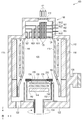
- FIG. 2 is a diagram schematically showing a configuration example of the film forming apparatus according to the embodiment.
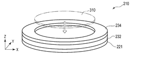
- FIG. 3 is a perspective view showing an outline of a configuration example of the susceptor unit according to the embodiment.
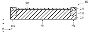
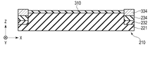
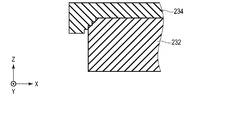
- FIG. 4 is a sectional view showing an outline of a configuration example of the susceptor unit according to the embodiment.
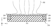
- FIG. 5A is a schematic diagram for explaining the flow of the process gas during the film forming process, and is a diagram showing a case where the height difference between the upper surface of the side guide of the susceptor unit and the upper surface of the wafer is small.
- FIG. 5B is a schematic diagram for explaining the flow of the process gas during the film forming process, and is a diagram showing a case where the height difference between the upper surface of the side guide of the susceptor unit and the upper surface of the wafer is large.
- FIG. 6A is a cross-sectional view showing an outline of a configuration example of a susceptor unit according to an embodiment, and is a view showing a case where a deposit is formed on a side surface guide of the susceptor unit.
- FIG. 6B is a schematic cross-sectional view of a configuration example of the susceptor unit according to the embodiment, and is a diagram showing a case where a deposit is further formed on the side surface guide of the susceptor unit.
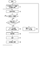
- FIG. 7 is a flowchart showing an outline of an example of a procedure when the film forming process is repeated in the embodiment.
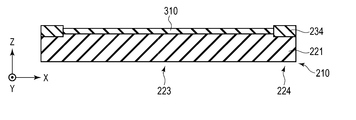
- FIG. 8A is a cross-sectional view schematically showing a configuration example of a susceptor unit according to the first modification.
- FIG. 8B is a cross-sectional view schematically showing a configuration example of the susceptor unit according to the first modification, and is a diagram showing a case where a deposit is formed on the side surface guide of the susceptor unit.
- FIG. 8C is a cross-sectional view schematically showing a configuration example of the susceptor unit according to the first modification, and is a diagram showing a case where a deposit is further formed on the side surface guide of the susceptor unit.
- FIG. 8A is a cross-sectional view schematically showing a configuration example of a susceptor unit according to the first modification.
- FIG. 8B is a cross-sectional view schematically showing a configuration example of the susceptor unit according to the first modification, and
- FIG. 9A is a cross-sectional view showing an outline of a configuration example of a susceptor unit according to the second modification.
- FIG. 9B is a cross-sectional view schematically showing a configuration example of the susceptor unit according to the second modification, and is a diagram showing a case where a deposit is formed on the side surface guide of the susceptor unit.
- FIG. 9C is a cross-sectional view schematically showing a configuration example of the susceptor unit according to the second modification, and is a diagram showing a case where a deposit is further formed on the side surface guide of the susceptor unit.
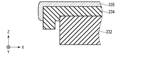
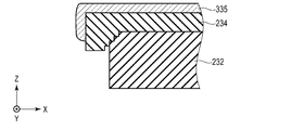
- FIG. 10A is a sectional view showing a part of the outline of the configuration example of the susceptor unit according to the third modification.
- FIG. 10B is a cross-sectional view showing a part of the outline of the configuration example of the susceptor unit according to the third modified example, and is a view showing a case where a film is deposited on the side surface guide of the susceptor unit.
- FIG. 10C is a cross-sectional view showing a part of the outline of the configuration example of the susceptor unit according to the third modification, and is a diagram showing a case where a deposit is further formed on the side surface guide of the susceptor unit.
- FIG. 11A is a cross-sectional view showing a part of the outline of the configuration example of the susceptor unit according to the fourth modification.
- FIG. 11B is a cross-sectional view showing a part of the outline of the configuration example of the susceptor unit according to the fourth modification, and is a diagram showing a case where a deposit is formed on the side surface guide of the susceptor unit.
- FIG. 11C is a cross-sectional view showing a part of the outline of the configuration example of the susceptor unit according to the fourth modified example, and is a view showing a case where a deposit is further formed on the side surface guide of the susceptor unit.
- the film forming system according to the embodiment will be described with reference to the drawings.
- the film forming system of this embodiment is a system for forming a film by using a CVD method.
- the wafer on which the film is formed is held by the susceptor unit and placed in the film forming chamber. Although a film is formed on the upper surface of the wafer in the film forming chamber, a deposit is also formed on the upper surface of the susceptor unit.
- the film forming system when the film formation on the wafer is completed, the wafer is removed from the susceptor unit. Then, in the film forming system, another wafer is held in the susceptor unit to form a film.
- the deposit on the upper surface of the susceptor unit becomes thick.
- This embodiment is devised so that the deposition conditions on the wafer do not change even if a deposit is formed on the upper surface of the susceptor unit.
- the spacer (adjustment member) provided on the susceptor unit is appropriately changed to a spacer having a different thickness so that the height difference between the upper surface of the wafer and the upper surface of the susceptor unit does not change beyond an allowable value. Can be replaced.
- the technique according to the present embodiment can be used for a film forming process using a CVD method, another vapor phase growth method, or another epitaxial growth method.
- the film forming system 1 includes a preparation chamber 10 and a transfer chamber 20. Further, the film forming system 1 includes a first load lock chamber 30a, a second load lock chamber 30b, a first susceptor replacement chamber 40a, a second susceptor replacement chamber 40b, and a first film formation chamber. 50a and the 2nd film formation chamber 50b are provided. The first load lock chamber 30a and the second load lock chamber 30b are equivalent to each other, the first susceptor exchange chamber 40a and the second susceptor exchange chamber 40b are equivalent to each other, and The film chamber 50a and the second film forming chamber 50b are equivalent.
- the film forming system 1 has two systems of film forming apparatuses for forming a film.
- the film forming system 1 includes a first load lock chamber 30a, a first susceptor replacement chamber 40a, and a first film forming chamber 50a, a first system, a second load lock chamber 30b, and a first load lock chamber 30b.
- the second system includes a second susceptor replacement chamber 40b and a second film formation chamber 50b.
- the first load lock chamber 30a is connected to the preparation chamber 10 via the first gate valve 32a, and is connected to the transfer chamber 20 via the second gate valve 34a.
- the second load lock chamber 30b is connected to the preparation chamber 10 via the third gate valve 32b, and is connected to the transfer chamber 20 via the fourth gate valve 34b. Wafers can be transferred between the preparation chamber 10 and the transfer chamber 20 by the first load lock chamber 30a and the second load lock chamber 30b.
- the first susceptor exchange chamber 40a is connected to the outside via the fifth gate valve 42a, and is also connected to the transfer chamber 20 via the sixth gate valve 44a.
- the second susceptor exchange chamber 40b is connected to the outside via the seventh gate valve 42b, and is connected to the transfer chamber 20 via the eighth gate valve 44b.
- the first susceptor replacement chamber 40a and the second susceptor replacement chamber 40b allow the susceptor unit to be transported between the outside and the transfer chamber 20.
- the first film forming chamber 50a is connected to the transfer chamber 20 via the ninth gate valve 52a.
- the second film forming chamber 50b is connected to the transfer chamber 20 via the tenth gate valve 52b.
- a robot 22 is provided in the transfer chamber 20.
- the robot 22 mounts the wafer or the susceptor unit on which the wafer is placed on the first load lock chamber 30a, the second load lock chamber 30b, the first susceptor replacement chamber 40a, the second susceptor replacement chamber 40b, and the first susceptor replacement chamber 40b.
- the film forming chamber 50a or the second film forming chamber 50b is configured to be transported in and out.
- the preparation room 10 is provided with a robot 12, an aligner 14, a first cassette 16a, and a second cassette 16b.
- a wafer transferred via the first load lock chamber 30a is placed on the first cassette 16a.
- a wafer transferred via the second load lock chamber 30b is placed on the second cassette 16b.
- the wafer is transferred between the preparation chamber 10 and the first load lock chamber 30a and between the preparation chamber 10 and the second load lock chamber 30b.
- a susceptor unit is loaded into the first susceptor replacement chamber 40a from the outside via the fifth gate valve 42a. Similarly, the susceptor unit is loaded into the second susceptor exchange chamber 40b from the outside via the seventh gate valve 42b.
- the robot 22 of the transfer chamber 20 takes out the wafer in the first load lock chamber 30a via the second gate valve 34a and places it on the susceptor unit carried into the first susceptor exchange chamber 40a.
- the robot 22 takes out the susceptor unit in which the wafer in the first susceptor exchange chamber 40a is placed from the first susceptor exchange chamber 40a and places it in the first film formation chamber 50a.
- a CVD method is used to form an epitaxial film of, for example, SiC on the upper surface of the wafer.
- the susceptor unit is composed of carbon, SiC, carbon coated with SiC, carbon coated with TaC, or the like. Further, for the individual parts constituting the susceptor unit, these materials can be individually selected according to the purpose.
- the robot 22 of the transfer chamber 20 takes out the susceptor unit holding the film-formed wafer from the first film-forming chamber 50a and places it in the first susceptor exchange chamber 40a.
- the robot 22 takes out the film-formed wafer from the susceptor unit in the first susceptor exchange chamber 40a and puts it in the first load lock chamber 30a.
- the film-formed wafer in the first load lock chamber 30a is taken out by the robot 12 in the preparation chamber 10 and placed in the first cassette 16a.
- a cassette may be provided in the first load lock chamber 30a and the first susceptor replacement chamber 40a, and a plurality of wafers may be placed in each chamber.
- the film forming system 1 includes a control device 80 that controls the operation of each unit of the film forming system 1.
- the control device 80 includes a CPU (Central Processing Unit) 81, a RAM (Random Access Memory) 82, a ROM (Read Only Memory) 83, a storage 84, an input device 85, which are connected to each other via a bus line.
- a display device 86 and an interface (I/F) 87 are provided.
- the CPU 81 performs various signal processing and the like.
- the operation of the CPU 81 is performed according to the programs and data stored in the RAM 82 and the ROM 83, for example.
- the storage 84 for example, an HDD (Hard Disk Drive), an SSD (Solid State Drive), or the like is used.
- the storage 84 stores various kinds of information such as programs and parameters necessary for executing the functions of the control device 80.
- the programs required for the operation of the control device 80 are loaded from the storage 84 into the RAM 82 and executed by the CPU 81.
- the ROM 83 loads the program from the storage 84 to the RAM 82 when the control device 80 is activated, and thus may store the boot processing program. Any type of device may be used for each device as long as it has an equivalent function.
- the control device 80 is connected to each part of the film forming system 1 via the I/F 87 in order to control each part of the film forming system 1, and inputs and outputs information necessary for the control.
- the X direction and the Y direction are parallel to the upper surface of the wafer to be deposited, and the Z direction (orthogonal to the X direction and the Y direction) are It corresponds to the vertical direction with respect to the upper surface.
- FIG. 2 is a diagram schematically showing a configuration example of the film forming apparatus 100 provided in the first film forming chamber 50a and the second film forming chamber 50b.
- the film forming apparatus 100 shown in FIG. 2 is a hot wall type thermal CVD apparatus.
- the film forming apparatus 100 is used for forming a SiC epitaxial film, for example.
- the film forming apparatus 100 includes a chamber 112 as a film forming chamber.
- a cylindrical hot wall 116 for example, is provided in the chamber 112, and the inside of the hot wall 116 serves as a film formation region 120 as a reaction chamber.
- the wafer 310 is placed on the susceptor unit 210 below the film formation region 120 in the Z direction.
- Process gas is supplied to the film formation region 120 from a gas supply unit 160 (supply port) provided above in the Z direction.
- the process gas reacts on the upper surface of the wafer 310 held by the susceptor unit 210, and a SiC epitaxial film, for example, is formed by a vapor phase growth reaction.
- the susceptor unit 210 is placed on the rotation holder 150.
- the rotation holder 150 has a cylindrical portion 152 and a rotation shaft 154 fixed to the lower portion of the cylindrical portion 152.
- the cylindrical portion 152 is configured such that the susceptor unit 210 is placed on the upper portion thereof.
- the cylindrical portion 152 has a large opening on the side on which the susceptor unit 210 is placed.
- a motor (not shown) is connected to the rotating shaft 154.
- the rotation holder 150 is configured to rotate by this motor.
- the rotation holder 150 rotates, so that the wafer 310 held by the susceptor unit 210 placed thereon rotates.
- the susceptor unit 210 holding the wafer 310 is transferred to the chamber 112 via the carry-in port 126.
- a bottom heater 132 is provided inside the cylindrical portion 152.
- the bottom heater 132 heats the wafer 310 from its back surface through the opening of the cylindrical portion 152 and the lower portion of the susceptor unit 210.
- the bottom heater 132 includes a disc-shaped in-heater 133 arranged in the center and an annular out-heater 134 arranged on the outer periphery of the in-heater 133.
- a heating heater with electric resistance can be used as the in-heater 133 and the out-heater 134.
- the in-heater 133 and the out-heater 134 can be made of carbon having a predetermined resistance value, SiC, carbon coated with SiC, carbon coated with TaC, or the like.
- the bottom heater 132 is powered by wiring (not shown) provided in the rotating shaft 154.
- the reflector 142 is made of a material having a high heat resistance such as carbon, SiC, carbon coated with SiC, carbon coated with TaC, or the like.
- the reflector 142 may be composed of one plate, or may be composed of a plurality of plates laminated. The reflector 142 contributes to suppressing power consumption of the heater during heating.
- a heat insulating material 144 is provided below the reflector 142 in the Z direction.
- the reflector 142 and the heat insulating material 144 prevent the heat of the bottom heater 132 from being transferred downward in the Z direction of the film forming apparatus 100.
- the hot wall 116 provided laterally in the chamber 112 is made of a highly heat-resistant material such as carbon, SiC, carbon coated with SiC, carbon coated with TaC, or the like.
- a side heater 138 is provided outside the hot wall 116 in the chamber 112. The side heater 138 can also be a heater that uses electrical resistance. The heat generated by the side surface heater 138 heats the film formation region 120, the wafer 310, the susceptor unit 210, and the like via the hot wall 116.
- a heat insulating material 118 is provided between the side heater 138 and the inner wall of the chamber 112. The heat insulating material 118 prevents the heat of the side heater 138 from being transferred to the wall of the chamber 112.
- an exhaust port 122 for exhausting gas is provided.
- the exhaust port 122 is connected to an exhaust mechanism having a regulating valve and a vacuum pump (not shown).
- the inside of the chamber 112 is adjusted to a predetermined pressure via an exhaust mechanism.
- a reflector 124 that reflects radiant heat from the bottom heater 132 and the side heater 138 is provided above the film formation region 120 in the chamber 112 in order to improve thermal efficiency.
- the reflector 124 can be composed of a plate using carbon, SiC, carbon covered with SiC, carbon covered with TaC, or the like.
- the reflector 124 may be configured by one plate or may be configured by stacking a plurality of plates.
- a plurality of gas holes (not shown) may be provided in the reflector 124 to supply the rectifying gas from the upper space of the reflector 124 to the film formation region 120.
- the rectifying gas By supplying the rectifying gas, the convection of the gas in the vicinity of the reflector 124 in the film formation region 120 is suppressed, and the deposition of the deposit on the reflector 124 is suppressed.
- Gas can be introduced into the upper space of the reflector from a gas pipe (not shown). Hydrogen gas, argon gas, or the like is used as the rectifying gas.
- a gas supply unit 160 is provided above the chamber 112.
- the gas supply unit 160 supplies a process gas such as a carrier gas, a source gas, or a doping gas to the film formation region 120.
- the gas supply unit 160 includes, for example, a first gas pipe 1611, a first partition plate 1612, a first gas pipe 161, a second gas pipe 1621, a second partition plate 1622, and a second gas.
- a pipe 162, a third gas pipe 1631, a third partition plate 1632, and a third gas pipe 163 are provided. Gas is supplied from the first gas pipe 161 to the first gas pipe 1611, gas is supplied from the second gas pipe 162 to the second gas pipe 1621, and gas is supplied to the third gas pipe 1631 by the third gas pipe 1631.
- Gas is supplied from the gas pipe 163.
- the partition plates 1612, 1622, 1632 prevent the gases supplied from the gas pipes 161, 162, 163 from being mixed inside the gas supply unit 160.
- the first gas pipe 1611 supplies, for example, hydrogen gas to the deposition region 120.
- the second gas pipe 1621 supplies, for example, a silane gas as a SiC source gas, an HCl gas for improving a growth rate, and a hydrogen gas as a carrier gas thereof to the film formation region 120.
- the third gas pipe 1631 supplies, for example, propane gas as a SiC source gas, nitrogen gas as a doping gas, and hydrogen gas as a carrier gas thereof to the film formation region 120. Note that FIG.
- the actual gas supply unit 160 includes a first gas pipe 1611, a second gas pipe 1621, and a third gas pipe 1631, respectively. It is possible to have a plurality. Further, the arrangement of the first gas pipe 1611, the second gas pipe 1621, and the third gas pipe 1631 is not particularly limited, and any arrangement that can enhance the uniformity such as the film thickness distribution and the carrier concentration distribution can be arbitrarily set. You can choose.
- a radiation thermometer 171 is provided above the gas supply unit 160 for the purpose of measuring the temperature of the wafer 310.
- the radiation thermometer 171 measures the temperature of the wafer 310 through a window 172 made of quartz glass provided on the gas supply unit 160 and a pipe 173.
- the radiation thermometer 171 monitors the temperature at a plurality of points from the central portion of the wafer 310 to the outer peripheral portion.
- the pressure inside the chamber 112 is adjusted to 26.7 kPa, for example.
- the wafer 310 is heated to 1500° C. or higher using the bottom heater 132 and the side heater 138.
- the temperature of the upper surface of the wafer 310 is monitored by using the radiation thermometer 171.
- the temperature is maintained at 1620° C. within ⁇ 1° C.
- the wafer 310 is rotated by the rotation holder 150 at, for example, 600 rpm.
- the SiC epitaxial film is formed on the upper surface of the wafer 310.
- a SiC film having a thickness of, for example, 5 ⁇ m to 10 ⁇ m (hereinafter, the length in the Z direction) is formed over about 30 to 45 minutes.
- FIG. 3 is a perspective view showing an outline of a configuration example of the susceptor unit 210.
- FIG. 4 is a sectional view showing an outline of a configuration example of the susceptor unit 210.
- the susceptor unit 210 includes at least a back surface support member 221, a spacer 232, and a side surface guide 234.
- the back surface support member 221 is a support member that supports the wafer 310.
- the back surface support member 221 as an example has a substantially disc shape.
- the back surface supporting member 221 has a disk-shaped central portion 223 having a top surface and a bottom surface that are parallel to each other and is flat, and has a diameter substantially the same as that of the wafer 310, and is around the central portion 223 and slightly thinner than the central portion 223. And a peripheral portion 224.
- the spacer 232 as an example has an annular shape.
- the spacer 232 is configured to be placed on the peripheral edge portion 224 of the back surface support member 221. That is, the inner diameter of the spacer 232 is, for example, substantially the same as the diameter of the central portion 223 of the back surface support member 221.
- the outer diameter of the spacer 232 is, for example, substantially the same as the outer diameter of the back surface support member 221.
- the spacer 232 is fitted into the back surface support member 221 so as to surround the central portion 223 of the back surface support member 221.
- the thickness of the spacer 232 is thinner than the difference in thickness between the central portion 223 and the peripheral portion 224 of the back surface support member 221.
- the spacer is an adjusting member for adjusting the position of the upper surface of the side surface guide 234 with respect to the upper surface of the wafer 310, as described later.
- the side guide 234 as an example has an annular shape.
- the side surface guide 234 is configured to be placed on the spacer 232. That is, the inner diameter of the side surface guide 234 is, for example, substantially the same as the diameter of the central portion 223 of the back surface support member 221.
- the outer diameter of the side surface guide 234 is, for example, substantially the same as the outer diameter of the back surface support member 221.
- the side surface guide 234 is fitted into the back surface support member 221 so as to surround the central portion 223 of the back surface support member 221.
- the side surface guide 234 is configured to be provided on the support member so as to surround the outer periphery of the wafer 310 when viewed from the direction (Z direction) perpendicular to the film formation surface of the wafer 310. ..
- the upper surface of the side surface guide 234 is configured to be higher than the central portion 223 of the back surface support member 221. That is, when the spacer 232 and the side surface guide 234 are fitted into the back surface support member 221, a recess is formed on the central portion 223 of the back surface support member 221.
- the wafer 310 is placed in this recess. Since the outer periphery of the wafer 310 is surrounded by the side guides 234, even when the susceptor unit 210 that holds the wafer 310 is rotated by the rotation holder 150 during film formation, the wafer 310 does not shift due to centrifugal force.
- the thickness of the wafer 310 is not limited to this, but is, for example, about 350 ⁇ m.
- the thickness of the spacer 232 is the thickest, and is set to, for example, about 3 mm. Considering the strength, the thickness of the spacer 232 is preferably 300 ⁇ m or more.
- the thickness of the side surface guide 234 is, for example, about 1 mm.
- the diameter of the wafer 310 is, for example, about 100 to 150 mm.
- the width of the annular spacer 232 and the side guide 234 is, for example, about 10 mm.
- the position of the upper surface of the wafer 310 is preferably substantially the same as the position of the upper surface of the side surface guide 234 or slightly higher than the upper surface of the side surface guide 234. ..
- the position of the upper surface of the side guide 234 may be adjusted to be higher than the position of the upper surface of the wafer 310 by, for example, about 150 ⁇ m so that the wafer 310 is not displaced (FIG. 4). That is, the position of the upper surface of the side surface guide 234 with respect to the film formation surface of the wafer 310 is preferably within the above-described predetermined range.
- the back surface support member 221 can be made of, for example, carbon, SiC, carbon coated with SiC, carbon coated with TaC, or the like.
- carbon or carbon coated with TaC is preferably used as the back surface support member 221. This is because SiC or SiC-coated carbon may sublime SiC at a high temperature, and the sublimated SiC may be transferred to the back surface of the wafer 310.
- the side guide 234 can be made of, for example, carbon, SiC, carbon coated with SiC, carbon coated with TaC, or the like.
- the spacer 232 can be made of, for example, carbon, SiC, carbon covered with SiC, carbon covered with TaC, or the like.
- SiC can be used as the side surface guide 234.
- carbon, carbon coated with SiC, and carbon coated with TaC tend to warp during cooling due to the difference in coefficient of thermal expansion with the deposit (SiC) formed on the side surface guide 234.
- carbon or carbon coated with TaC can be used as the spacer 232. This is because one of the SiC and the carbon coated with SiC sublimes between the SiC and the SiC of the side guide 234 and is easily transferred to the other.
- the side guide 234 and the spacer 232 have the same specific heat and the same thermal conductivity.
- the difference between the specific heat of the side surface guide 234 and the specific heat of the spacer 232 is preferably 0.3 J/gK or less, for example.
- the specific heat of SiC varies depending on the manufacturing method, it is approximately 0.65 to 0.67 J/gK, whereas the specific heat of carbon is approximately 0.60 to 0.85 J/gK, which varies depending on the manufacturing method.
- the combination of SiC and carbon is suitable.
- the members that form the susceptor unit 210 need to have heat resistance that can withstand the temperature during the film formation process. Further, it is preferable that the specific heat of the spacer 232 and the specific heat of the material to be deposited are also the same.
- the difference between the specific heat of the spacer 232 and the specific heat of the material to be deposited is preferably 0.3 J/gK or less, for example.
- FIG. 5A is a diagram schematically showing the flow of the process gas 332 on the upper surface of the wafer 310 during film formation.
- the process gas 332 flows from the center toward the outside along the upper surface of the wafer 310.
- the process gas 332 smoothly flows to the outside of the susceptor unit 210 without being disturbed around the side surface guide 234. In this case, the process gas 332 does not stay in the peripheral portion of the wafer 310, and a good film thickness distribution and carrier concentration distribution can be obtained on the upper surface of the wafer 310.
- the film forming process not only the film is formed on the upper surface of the wafer 310, but also the deposit is formed on the upper surface of the side guide 234.
- deposits are successively formed on the upper surface of the side surface guide 234 and become thicker.
- the deposit formed and deposited on the upper surface of the side guide 234 becomes thicker.
- the height difference between the upper surface of the side surface guide 234 on which the deposit 334 is formed and the upper surface of the wafer 310 before the film forming process that is exchanged each time the film forming process is gradually increased.
- this height difference becomes large, turbulence occurs in the flow of the process gas 332.
- the process gas 332 accumulates in the peripheral portion of the wafer 310.
- Such a change in the flow of the process gas 332 may change the film thickness distribution of the film formed on the wafer 310, the carrier concentration distribution, and the like.
- the spacer 232 is replaced with a thinner one, as shown in FIGS. 6A and 6B. In this way, the height difference between the upper surface of the side guide 234 on which the deposit is formed and the upper surface of the wafer 310 is adjusted so as to be within a predetermined range.
- the spacer 232 is replaced.
- the spacer 232 is replaced when the thickness of the deposit 334 increases by 150 ⁇ m, for example, when a film of 10 ⁇ m is formed in one film forming process, the spacer 232 is formed every 15th film forming process. Will be replaced.
- the spacer to be replaced next is a spacer having a thickness of 2850 ⁇ m.
- a plurality of types of spacers 232 having different thicknesses are prepared, and they are exchanged according to the number of film formation processes.
- a spacer set having a plurality of spacers 232 is prepared.
- the back surface support member 221 is composed of one member, but the present invention is not limited to this.
- the back surface support member 221 may be composed of a plurality of members.
- the back surface support member 221 may be configured such that the central portion thereof is lifted up so that the wafer 310 can be easily placed on the susceptor unit 210 and taken out from the susceptor unit 210.
- the lifting central portion and the other portions are configured as separate bodies, and function as the back surface supporting member 221 as a whole.
- 6A and 6B show a mode in which the upper surface of the back surface supporting member 221 is in contact with the back surface of the wafer 310.
- the back surface support member 221 has, for example, a stepped structure on the top surface of the back surface support member 221, so that a space is provided between the top surface of the back surface support member 221 and the back surface of the wafer 310. Good.
- a sequential film formation process for a plurality of wafers 310 using the film formation system 1 according to this embodiment will be described.
- the method described here is a continuous film forming method including replacement of the spacer 232 and the side surface guide 234. All the processes shown here may be fully automatically performed under the control of the control device 80.
- the control device 80 outputs a signal for control to each unit that operates. Further, a part of the processing shown here may be manually performed by the operator.
- the control device 80 may present information on the work to be performed by the operator on the display device 86. That is, the control device 80 outputs data or a signal for displaying the information to the display device 86.
- step S1 the total film thickness of the film deposited on the upper surface of the side surface guide 234 is set to the initial value.
- the total film thickness is set to 0 ⁇ m.
- a predetermined value is cumulatively added to the total film thickness every time the film forming process is performed until the total film thickness is reset to the initial value (step S9 ⁇ step S1). ..
- a deposit having a thickness approximately equal to the film thickness of a predetermined film thickness formed on the wafer 310 is formed on the upper surface of the side surface guide 234 by one film forming process on the wafer 310.
- the design value is used as the predetermined value added to the total film thickness. That is, since the film thickness formed on the wafer 310 by one film formation process on the wafer 310 is known as a design value, the total film thickness is calculated by repeating the film formation process every time the film formation process is repeated. (Film thickness) is added.
- the film formed on the wafer 310 and the thickness formed on the upper surface of the side surface guide 234 are significantly different from each other by one film formation process on the wafer 310, the film formed on the wafer 310.
- the total film thickness can be set by correlating the thickness with the film thickness of the deposit formed on the upper surface of the side surface guide 234.
- step S1 the spacer type indicator indicating which spacer is used among the plurality of spacers having different thicknesses is also set to the type of spacer used first.
- the new side guide 234 is used and the thickest spacer 232 is used, it is set to the indicator that indicates the thickest spacer.
- another spacer 232 is used, it is set to an indicator corresponding to that type of spacer.
- the information of the total film thickness and the indicator of the spacer type is stored in, for example, the RAM 82 or the storage 84 and used for processing. These pieces of information stored in the RAM 82 or the storage 84 can be updated by the processing of steps S5, S8, and S9 described below.
- step S2 the upper surface of the side guide 234 on which the deposit 334 is formed (the upper surface of the side guide 234 in the initial state because there is no deposit 334) and the film formation surface based on the current value of the total film thickness.
- the height difference from the upper surface of the wafer 310 is calculated.
- the position of the upper surface of the side surface guide 234 is obtained based on the total film thickness since the thickness of the spacer 232 corresponding to the type of the spacer 232 used and the thickness of the side surface guide 234 are known.
- the position of the upper surface of the wafer 310 is also determined by the known thickness of the wafer 310.
- step S3 it is determined whether or not the height difference calculated in step S2 is larger than the allowable value.
- the film forming process can be performed. Therefore, the process proceeds to S6, where the film forming preparation is performed and the film forming process is executed as described later.
- the allowable value is stored in the RAM 82 or the storage 84, for example, and can be set appropriately.
- step S3 When it is determined in step S3 that the height difference is larger than the allowable value, the process proceeds to step S4.
- step S4 it is determined whether there is a replaceable spacer. Replaceable spacers are spacers that are thinner than the spacers currently in use. When it is determined in step S4 that there is a replaceable spacer, the process proceeds to step S5.
- the spacer 232 is replaced in step S5. That is, in the susceptor replacement chamber, the side guide 234 and the spacer 232 are removed from the back surface supporting member 221, and a thinner spacer is placed instead of the spacer that has been used until then and the spacer that has been used is removed. The side guide 234 is placed. At this time, the stored indicator showing the type of spacer in use is changed to the indicator showing the type of spacer after replacement.
- the replacement of the spacer 232 may be performed manually by an operator, or a dedicated device may be provided. Thereafter, the process proceeds to step S6. That is, as shown below, the film formation preparation is performed and the film formation process is executed.
- step S6 film forming preparations such as transfer of the wafer 310 and the susceptor unit 210 into the chamber 112 and adjustment of the temperature in the chamber 112 are performed.
- step S7 a film forming process is executed. That is, the susceptor unit 210 is rotated using the rotation holder 150 in the chamber 112 heated to an appropriate temperature. In this state, the process gas is supplied, and a film such as a SiC crystal film is formed on the wafer 310. At the same time, a deposit of SiC, for example, is also formed on the upper surface of the side guide 234.
- step S8 for example, the total film thickness is formed on the wafer 310 by the film forming process of step S7. Formed on the upper surface of the side surface guide 234, which is obtained from the relationship between the film thickness of the deposited film formed on the upper surface of the side surface guide 234 and the film thickness of the film formed on the wafer 310 which has been examined in advance. The thickness of the deposited deposit is added. The stored total film thickness is updated to a value indicating the film thickness of the deposit on the side surface guide 234 after the film forming process. That is, the total film thickness is updated based on the film thickness formed on the wafer 310. After that, the process returns to step S2 to calculate the height difference and determine whether the next film formation is allowed.
- step S9 the side surface guide 234 and the spacer 232 are exchanged. That is, in the spacer exchange chamber, the side guides 234 and the spacers 232 which have been used until now are removed from the back surface supporting member 221, and instead, the thickest spacers 232 are placed and the deposit 334 is formed thereon. A new or cleaned side guide 234 is placed. The spacers used so far can be used repeatedly. Then, the process proceeds to step S1.
- the stored total film thickness is reset to 0 ⁇ m, and the indicator corresponding to the type of the thickest spacer is set to the stored indicator indicating the type of spacer in use.
- the subsequent processing is the same as described above. These procedures are repeated while the series of film forming processes are repeated, and are ended when the series of film forming processes is completed.
- the height difference between the upper surface of the side guide 234 (the upper surface of the deposit 334) and the upper surface of the wafer 310 falls within a predetermined range by replacing the spacer 232. Therefore, in the film forming process, the flow of the process gas on the upper surface of the wafer 310 does not change even if the film forming process is repeated, which influences the film thickness and the properties of the film to be formed.
- the specific heat of the spacer 232, the side guide 234, and the deposit 334 is almost the same. Further, even if the thickness of the deposit 334 is increased, the total volume of the spacer 232, the side surface guide 234, and the deposit 334 is within the allowable range. Therefore, the heat capacity of the spacer 232, the side guides 234, and the deposit 334 together becomes constant within an allowable range even if the deposit 334 becomes thick. That is, the temperature of the outer peripheral portion of the wafer 310 can be kept constant within an allowable range.
- the position of the upper surface of the wafer 310, which is the target of the film formation process, in the chamber 112 does not change during the repeated film formation processes. Further, the form in which the wafer 310 is placed on the susceptor unit 210 does not change. From the above, even if the deposit 334 becomes thicker or the spacer 232 is replaced, the film forming conditions can be made constant through repeated film forming processes. As a result, the film formed on the wafer 310 also becomes uniform.
- the position of the wafer 310 that is the target of the film formation process in the chamber 112 does not change during the repeated film formation processes. That is, even if the film forming process is repeated, the position of the upper surface of the wafer 310 to be film formed does not change with respect to the other components of the chamber 112. This means that it becomes easy to stably obtain information for grasping the state of the film forming process, such as temperature measurement by the radiation thermometer 171. This point also contributes to making the film formed on the wafer 310 uniform.
- the present embodiment is particularly effective when a SiC film is formed. It is possible to remove the deposit by performing a cleaning process on the side guide 234 on which the deposit 334 is formed.
- the cleaning process is a process of removing deposits formed on the side surface guide 234 by a chemical process or a process of mechanically scraping.
- the composition of the deposit 334 formed on the upper surface of the side guide 234 is Si or GaN
- a cleaning method using such a gas has not been established.
- the side guide 234 on which the SiC deposit is formed needs to remove the SiC deposit by, for example, polishing. Mechanical cleaning is time-consuming and may damage the side guides 234. Further, even in the case of the chemical treatment, for example, when the composition of the deposit is SiC and the side guide 234 is also made of SiC, a part of the side guide is removed together with the removal of the deposit (over). Etching). That is, it is difficult to remove only the SiC deposits formed on the upper surface of the side surface guide 234, and even if it is possible, it is expensive.
- the film thickness formed on the wafer 310 in a single film forming process is generally relatively thick, such as 5 ⁇ m or more.
- the film thickness of the deposit 334 on the side guide 234 that does not affect the film thickness distribution of the film formed on the wafer 310 is limited to about 150 to 500 ⁇ m. Therefore, since the limit is reached with a small number of film forming processes, the height difference between the upper surface of the side surface guide 234 and the upper surface of the wafer 310 as described with reference to FIG. 5B is likely to be a problem. Therefore, if no measures are taken, the side guide 234 will be replaced more frequently, and its cost will be a problem.
- the above problems can be solved without providing a special mechanism such as a lifting mechanism using a motor in the susceptor unit 210 or the film forming apparatus 100.
- the positional relationship between the susceptor unit 210 and the constituent elements of the film forming apparatus 100 such as the heater, the gas supply unit 160, the radiation thermometer 171 and the like does not change. Therefore, while maintaining the setting conditions of the film forming apparatus 100 for the wafer 310, the above problem can be solved by a simple method of replacing the spacer 232.
- the bottom heater 132 is provided below the susceptor unit 210, and heating is performed from below the susceptor unit 210.
- the lower portion of the susceptor unit 210 does not change.
- the positional relationship between the back surface supporting member 221 and the out heater 134 or the positional relationship between the back surface supporting member 221 and the wafer 310 does not change. Therefore, various conditions do not change during the repetition of the film forming process, and the effect that the adjustment of the film forming condition becomes unnecessary or easy is obtained.
- a plurality of spacers having different thicknesses are prepared as the spacer 232, and the spacer to be used is selected according to the film thickness of the deposit 334 formed. However, it is not limited to this. Whether to insert the spacer 232 may be selected depending on the film thickness of the deposit 334. Further, the number of the spacers 232 simultaneously inserted into the susceptor unit 210 is not limited to one. A plurality of spacers 232 may be inserted, and the thickness may be adjusted depending on the number of spacers 232. However, if the spacer 232 has a certain thickness, it is easier to handle and has higher durability. Therefore, when a plurality of spacers 232 are used, the thickness of the spacer 232 should be determined in consideration of ease of handling. In either case, the spacer 232 is selectively inserted depending on the thickness of the deposit.
- FIGS. 8A, 8B, and 8C A schematic diagram of this modification is shown in FIGS. 8A, 8B, and 8C.
- FIG. 8A when there is no deposit on the side surface guide 234, the wafer 310 is placed on the back surface supporting member 221.
- FIG. 8B when a deposit 334 is formed on the side surface guide 234, a spacer 242 having a thickness corresponding to the thickness of the deposit 334 is placed on the back surface supporting member 221, and a wafer is placed on the spacer 242. 310 is placed.
- FIG. 8C when the deposit 334 becomes thicker, the spacer 242 is replaced with a thicker one accordingly.
- the shape of the spacer 242 may not support the entire back surface of the wafer 310, such as a ring shape.
- the height difference between the upper surface of the deposit 334 on the side surface guide 234 and the upper surface of the wafer 310 is within a predetermined range. Therefore, similar to the above-described embodiment, the flow of the process gas on the upper surface of the wafer 310 does not undergo unacceptable changes such as disturbances through the repeated film forming processes. Therefore, the film formed on the wafer 310 is uniform.
- the back surface support member 221 may be replaced. That is, as shown in FIGS. 9A, 9B, and 9C, depending on the film thickness of the deposit 334 on the side surface guide 234, the central portion 223 or the peripheral edge portion 224, or both the central portion 223 and the peripheral edge portion 224 may be formed.
- An appropriate back surface support member 221 may be selected from a plurality of back surface support members 221 having different film thicknesses. The back surface support member 221 does not have to have a structure that supports the entire back surface of the wafer 310.
- the height difference between the upper surface of the side surface guide 234 and the upper surface of the wafer 310 is within a predetermined range. Therefore, the flow of the process gas on the upper surface of the wafer 310 does not undergo unacceptable changes such as turbulence during the repeated film forming processes. Furthermore, the back surface supporting member 221, the side surface guide 234, and the deposit 334 are adjusted so that their combined sizes are almost the same, so that their heat capacities, the position of the upper surface of the wafer 310, and the configuration of the back surface side of the wafer 310 are adjusted. Does not change. As a result, it is not necessary to change the setting conditions of the film forming apparatus 100 for the wafer 310, and the film formed on the wafer 310 becomes uniform.
- the number of parts can be reduced by not using spacers.
- the spacer by using the spacer, the back surface support member 221 can be shared.
- the first modified example, and the second modified example may be used in combination. That is, the spacer 232 inserted between the back surface support member 221 and the side surface guide 234 and the spacer 242 inserted between the back surface support member 221 and the wafer 310 are used at the same time, or the back surface support member 221 is It may be exchanged.
- the reaction product of the process gas may adhere not only to the upper surface of the side surface guide 234 but also to the side surface of the side surface guide 234 and the spacer 232. Furthermore, the reaction product may also enter between the spacer 232 and the side guide 234 due to processing variations between the spacer 232 and the side guide 234. When the reaction product enters between the side surface guide 234 and the spacer 232 and the reaction product adheres to one of the side surface guide 234 and the spacer 232, the adhesion between the spacer 232 and the side surface guide 234 gradually deteriorates. Therefore, the side guide 234 may partially float from the spacer 232.
- Such a state causes rattling between the side guides 234 and the spacers 232, which adversely affects the stability when the rotary holder 150 rotates at high speed. Further, the contact areas of the side guides 234 and the spacers 232 are different, which makes it difficult to keep the temperature of the outer peripheral portion of the wafer 310 constant within an allowable range.
- the shape of the peripheral edge portion of the side surface guide 234 may be a shape that covers the spacer 232.
- the reaction product 335 is less likely to enter the interface between the side surface guide 234 and the spacer 232 as shown in FIGS. 10B and 10C.
- the spacer 232 and the side surface guide 234 may be configured so that the outer diameter of the spacer 232 can be changed.
- the peripheral edge of the side surface guide 234 is shaped so as to cover the spacer 232.
- the outer diameter of the spacer 232 is not changed when the reaction product 335 does not go around under the outer periphery of the side surface guide 234.
- FIG. 11C when the adhesion of the reaction product 335 further increases and goes around to the lower side of the outer periphery of the side surface guide 234, the spacer 232 is replaced with a spacer having a smaller outer diameter.
- the spacer 232 and the side guide 234 may be configured so that the attached reaction product 335 does not affect the interface between the side guide 234 and the spacer 232. ..
- a gap may be provided between the side surface of the wafer 310 and the inner side surface of the side surface guide 234 in consideration of processing variations, thermal expansion, transfer accuracy of the wafer 310, and the like. Further, a gap may be provided between the inner side surfaces of the spacer 232 and the side surface guide 234 and the side surface of the central portion 223 of the back surface support member 221 in consideration of processing variations and thermal expansion.
- the deposit 334 is formed not only on the upper surface of the side surface guide 234 but also on the inner side surface of the side surface guide 234, and it may protrude in the inner circumferential direction of the side surface guide 234.
- the wafer 310 may interfere with the wafer 310, and the wafer 310 may not be removable from the susceptor unit 210. Therefore, as the allowable value of the height difference shown in step S3 of FIG. 7, it is possible to determine not only the height difference but also the amount of protrusion.
- the amount of protrusion can be reflected in the allowable value in step S3 of FIG. 7 by obtaining the relationship with the film thickness formed on the wafer 310 in advance.
- a protruding portion of the deposit 334 can be removed in a short time by a simple grinding device. Therefore, between the steps S3 and S4, the side surface guide 234 is temporarily taken out and deposited. A step of grinding the protruding portion of the object 334 may be added.
Landscapes
- Chemical & Material Sciences (AREA)
- Chemical Kinetics & Catalysis (AREA)
- General Chemical & Material Sciences (AREA)
- Engineering & Computer Science (AREA)
- Materials Engineering (AREA)
- Mechanical Engineering (AREA)
- Metallurgy (AREA)
- Organic Chemistry (AREA)
- Inorganic Chemistry (AREA)
- Chemical Vapour Deposition (AREA)
Abstract
成膜方法は、ウェハを載置するための支持部材と、前記支持部材上に設けられ前記ウェハの外周の少なくとも一部を囲む側面ガイドと、前記ウェハの上面と前記側面ガイドの上面との位置を調整するためのスペーサと、を含むサセプタユニット上に前記ウェハを載置することと、載置された前記ウェハの上面に所定の膜を成膜するとともに前記側面ガイド上に膜を形成することと、 成膜された前記所定の膜の厚さに基づいて、前記スペーサを用いて前記ウェハの上面に対する前記側面ガイドの上面の位置を調整することと、前記位置が調整された前記サセプタユニット上に新たなウェハを載置して、新たな所定の膜を成膜すること、を含む。
Description
実施形態は、成膜方法、成膜装置、サセプタユニット、及びサセプタユニットに用いられるスペーサセットに関する。
エピタキシャル成長によって、ウェハの上面(成膜される面)に膜を成膜(deposit)する成膜装置が知られている。以下では、ウェハの上面に所定の膜を成膜することを成膜処理と記載する。例えば、化学気相堆積(Chemical Vapor Deposition: CVD)法を用いた成膜装置では、プロセスガスの濃度や化学反応温度などが管理された成膜チャンバが設けられる。ウェハは、成膜チャンバの内部のサセプタに載置され、ウェハの上面にプロセスガスが供給される。その結果、ウェハの上面に所定の膜が成膜される。
サセプタは、例えば、カーボン、SiC(炭化ケイ素)、SiCで被覆したカーボン、TaC(炭化タンタル)で被覆したカーボンなどで構成される。ウェハの上面に所定の膜を成膜する場合、ウェハの上面に膜が成膜されるのみならず、サセプタの上面にも堆積物が形成される。なお、種々の理由により、この時にサセプタの上面に形成される堆積物は、ウェハの上面に成膜される膜とは必ずしも同じ膜ではない。サセプタを用いて、成膜処理が繰り返されると、サセプタの上面の堆積物は厚くなる。その結果、エピタキシャル膜が成膜される前のウェハの上面に対する、成膜処理が繰り返されることにより膜が堆積したサセプタの上面の高さ方向の位置(以下、位置と記す)が変化し、成膜処理の条件(成膜条件)が変化することがある。このような成膜条件の変化は、得られる膜の厚さや、性質に影響を与えることがある。
例えば特許文献1には、ウェハの上面に対する堆積物が形成されたサセプタの上面の位置を調整するモータを備えたサセプタ装置が開示されている。
実施形態は、サセプタユニットに堆積物が形成されても、ウェハに対する成膜条件を維持しつつ、安定した成膜処理を実現することを目的とする。
実施形態の一態様によれば、成膜方法は、ウェハを載置するための支持部材と、前記支持部材上に設けられ前記ウェハの外周の少なくとも一部を囲む側面ガイドと、前記ウェハの上面と前記側面ガイドの上面との位置を調整するためのスペーサと、を含むサセプタユニット上に前記ウェハを載置することと、載置された前記ウェハの上面に所定の膜を成膜するとともに前記側面ガイド上に膜を形成することと、 成膜された前記所定の膜の厚さに基づいて、前記スペーサを用いて前記ウェハの上面に対する前記側面ガイドの上面の位置を調整することと、前記位置が調整された前記サセプタユニット上に新たなウェハを載置して、新たな所定の膜を成膜すること、を含む。
本発明によれば、サセプタユニット上に堆積物が形成されても、ウェハに対する成膜条件を維持しつつ、安定した成膜処理を実現できる。
実施形態に係る成膜システムについて図面を参照して説明する。本実施形態の成膜システムは、CVD法を用いて成膜を行うためのシステムである。その上面に成膜されるウェハは、サセプタユニットに保持されて成膜チャンバに載置される。成膜チャンバ内では、ウェハの上面に成膜されるが、サセプタユニットの上面にも堆積物が形成される。成膜システムにおいて、ウェハへの成膜が完了すると、サセプタユニットからウェハが取り外される。そして、成膜システムにおいては、サセプタユニットに他のウェハを保持し、成膜を行う。このように、ウェハを交換しながら成膜を繰り返すと、サセプタユニットの上面における堆積物は厚くなる。本実施形態は、サセプタユニットの上面に堆積物が形成されても、ウェハに対する成膜条件が変化しないように工夫されている。より具体的には、ウェハの上面と、サセプタユニットの上面との高低差が許容値を超えて変化しないように、サセプタユニットに設けられたスペーサ(調整部材)を、厚さが異なるスペーサに適宜に交換することができる。なお、本実施形態に係る技術は、CVD法や他の気相成長法、及びその他のエピタキシャル成長法を用いた成膜処理に用いることができる。
[システム構成]
〈成膜システム〉
本実施形態に係る成膜システム1の構成例の概略を図1に示す。成膜システム1は、準備室10と、トランスファチャンバ20とを備える。また、成膜システム1は、第1のロードロックチャンバ30aと、第2のロードロックチャンバ30bと、第1のサセプタ交換チャンバ40aと、第2のサセプタ交換チャンバ40bと、第1の成膜チャンバ50aと、第2の成膜チャンバ50bとを備える。第1のロードロックチャンバ30aと第2のロードロックチャンバ30bとは同等のものであり、第1のサセプタ交換チャンバ40aと第2のサセプタ交換チャンバ40bとは同等のものであり、第1の成膜チャンバ50aと第2の成膜チャンバ50bとは同等のものである。すなわち、成膜システム1は、成膜を行うための2つの系統の成膜装置を有する。具体的には、成膜システム1は、第1のロードロックチャンバ30a、第1のサセプタ交換チャンバ40a、及び第1の成膜チャンバ50aという第1系統と、第2のロードロックチャンバ30b、第2のサセプタ交換チャンバ40b、及び第2の成膜チャンバ50bという第2系統と、を備える。
〈成膜システム〉
本実施形態に係る成膜システム1の構成例の概略を図1に示す。成膜システム1は、準備室10と、トランスファチャンバ20とを備える。また、成膜システム1は、第1のロードロックチャンバ30aと、第2のロードロックチャンバ30bと、第1のサセプタ交換チャンバ40aと、第2のサセプタ交換チャンバ40bと、第1の成膜チャンバ50aと、第2の成膜チャンバ50bとを備える。第1のロードロックチャンバ30aと第2のロードロックチャンバ30bとは同等のものであり、第1のサセプタ交換チャンバ40aと第2のサセプタ交換チャンバ40bとは同等のものであり、第1の成膜チャンバ50aと第2の成膜チャンバ50bとは同等のものである。すなわち、成膜システム1は、成膜を行うための2つの系統の成膜装置を有する。具体的には、成膜システム1は、第1のロードロックチャンバ30a、第1のサセプタ交換チャンバ40a、及び第1の成膜チャンバ50aという第1系統と、第2のロードロックチャンバ30b、第2のサセプタ交換チャンバ40b、及び第2の成膜チャンバ50bという第2系統と、を備える。
第1のロードロックチャンバ30aは、第1のゲートバルブ32aを介して準備室10とつながっており、また、第2のゲートバルブ34aを介してトランスファチャンバ20とつながっている。同様に、第2のロードロックチャンバ30bは、第3のゲートバルブ32bを介して準備室10とつながっており、また、第4のゲートバルブ34bを介してトランスファチャンバ20とつながっている。第1のロードロックチャンバ30a及び第2のロードロックチャンバ30bによって、準備室10とトランスファチャンバ20との間で、ウェハの搬送を行うことができる。
第1のサセプタ交換チャンバ40aは、第5のゲートバルブ42aを介して外部とつながっており、また、第6のゲートバルブ44aを介してトランスファチャンバ20とつながっている。同様に、第2のサセプタ交換チャンバ40bは、第7のゲートバルブ42bを介して外部とつながっており、また、第8のゲートバルブ44bを介してトランスファチャンバ20とつながっている。第1のサセプタ交換チャンバ40a及び第2のサセプタ交換チャンバ40bによって、外部とトランスファチャンバ20との間で、サセプタユニットの搬送を行うことができる。
第1の成膜チャンバ50aは、第9のゲートバルブ52aを介してトランスファチャンバ20とつながっている。同様に、第2の成膜チャンバ50bは、第10のゲートバルブ52bを介してトランスファチャンバ20とつながっている。
トランスファチャンバ20には、ロボット22が設けられている。ロボット22は、ウェハ又はウェハが載置されたサセプタユニットを、第1のロードロックチャンバ30a、第2のロードロックチャンバ30b、第1のサセプタ交換チャンバ40a、第2のサセプタ交換チャンバ40b、第1の成膜チャンバ50a、又は第2の成膜チャンバ50bの内外に搬送するように構成されている。
準備室10には、ロボット12と、アライナ14と、第1のカセット16aと、第2のカセット16bとが設けられている。第1のカセット16aには、第1のロードロックチャンバ30aを介して搬送されるウェハが載置される。第2のカセット16bには、第2のロードロックチャンバ30bを介して搬送されるウェハが載置される。ロボット12及びアライナ14を用いて、ウェハは、準備室10と第1のロードロックチャンバ30aとの間、及び準備室10と第2のロードロックチャンバ30bとの間で搬送される。
第1のサセプタ交換チャンバ40aには、第5のゲートバルブ42aを介して外部からサセプタユニットが搬入される。同様に、第2のサセプタ交換チャンバ40bには、第7のゲートバルブ42bを介して外部からサセプタユニットが搬入される。
トランスファチャンバ20のロボット22は、第1のロードロックチャンバ30a内のウェハを第2のゲートバルブ34aを介して取り出し、第1のサセプタ交換チャンバ40aに搬入されたサセプタユニットの上に載置する。ロボット22は、第1のサセプタ交換チャンバ40a内のウェハが載置されたサセプタユニットを第1のサセプタ交換チャンバ40aから取り出し、第1の成膜チャンバ50a内に載置する。第1の成膜チャンバ50a内で、例えばCVD法により、ウェハの上面に、例えばSiCのエピタキシャル膜が成膜される。なお、サセプタユニットは、カーボン、SiC、SiCで被覆したカーボン、TaCで被覆したカーボンなどにより構成される。また、サセプタユニットを構成する個々の部品は、これらの材料を目的に応じて個別に選択することができる。
トランスファチャンバ20のロボット22は、成膜後のウェハを保持したサセプタユニットを第1の成膜チャンバ50aから取り出し、第1のサセプタ交換チャンバ40a内に載置する。ロボット22は、第1のサセプタ交換チャンバ40a内で、サセプタユニットから成膜後のウェハを取り出し、第1のロードロックチャンバ30a内に入れる。第1のロードロックチャンバ30a内の成膜後のウェハは、準備室10のロボット12によって取り出され、第1のカセット16aに入れられる。
このような工程が繰り返されて、複数のウェハに、順次、結晶膜が成膜される。なお、第1のロードロックチャンバ30a及び第1のサセプタ交換チャンバ40aにカセットが設けられ、各チャンバに複数のウェハが載置される構成であってもよい。
準備室10、第2のロードロックチャンバ30b、第2のサセプタ交換チャンバ40b、及び第2の成膜チャンバ50bの間でのウェハの搬送も同様である。
成膜システム1は、成膜システム1の各部の動作を制御する制御装置80を備える。制御装置80は、バスラインを介して互いに接続されたCPU(Central Processing Unit)81と、RAM(Random Access Memory)82と、ROM(Read Only Memory)83と、ストレージ84と、入力装置85と、表示装置86と、インターフェース(I/F)87とを備える。
CPU81は、各種信号処理等を行う。CPU81の動作は、例えば、RAM82、ROM83に記憶されたプログラムやデータに従って行われる。ストレージ84には、例えば、HDD(Hard Disk Drive)、SSD(Solid State Drive)等が用いられる。ストレージ84には、制御装置80の機能を実行するために必要なプログラム群、パラメータ等各種情報が記録されている。制御装置80の動作に必要なプログラムは、ストレージ84からRAM82にロードされ、CPU81によって実行される。ROM83は、制御装置80の起動時にストレージ84からRAM82にプログラムをロードするため、ブート処理プログラムを記憶してもよい。各デバイスには、同等の機能を有していればどのような種類のデバイスが用いられてもよい。I/F87を介して、制御装置80は、成膜システム1の各部の制御を行うために、成膜システム1の各部と接続され、制御のために必要な情報の入出力を行っている。
〈成膜装置〉
尚、以下で参照される図面において、X方向及びY方向(X方向に直交)は、成膜されるウェハの上面に平行であり、Z方向(X方向及びY方向に直交)は、ウェハの上面に対する鉛直方向に対応している。
尚、以下で参照される図面において、X方向及びY方向(X方向に直交)は、成膜されるウェハの上面に平行であり、Z方向(X方向及びY方向に直交)は、ウェハの上面に対する鉛直方向に対応している。
図2は、第1の成膜チャンバ50a及び第2の成膜チャンバ50bに設けられた成膜装置100の構成例の概略を示す図である。図2に示した成膜装置100は、ホットウォール型熱CVD装置である。成膜装置100は、例えばSiCエピタキシャル膜の成膜に用いられる。
成膜装置100は、成膜チャンバとしてのチャンバ112を備える。チャンバ112内には、例えば円筒型のホットウォール116が設けられ、ホットウォール116の内側が、反応室としての成膜領域120となっている。成膜領域120のZ方向における下方には、サセプタユニット210にウェハ310が載置される。成膜領域120には、Z方向における上方に設けられたガス供給部160(供給口)からプロセスガスが供給される。成膜装置100では、サセプタユニット210に保持されたウェハ310の上面でプロセスガスが反応し、気相成長反応によって、例えばSiCエピタキシャル膜が成膜される。
サセプタユニット210は、回転ホルダ150に載置される。回転ホルダ150は、円筒部152と、円筒部152の下部に固定された回転軸154とを有している。円筒部152は、その上部にサセプタユニット210が載置されるように構成されている。円筒部152は、サセプタユニット210が載置される側に大きな開口を有する。回転軸154には、図示しないモータが接続されている。回転ホルダ150は、このモータによって回転するように構成されている。成膜時には、回転ホルダ150が回転することで、そこに載置されたサセプタユニット210に保持されたウェハ310は回転する。なお、ウェハ310を保持しているサセプタユニット210は、搬入口126を介してチャンバ112に搬送される。
円筒部152の内部には、底部ヒータ132が設けられている。底部ヒータ132は、円筒部152の開口とサセプタユニット210の下部を介して、ウェハ310をその裏面から加熱する。底部ヒータ132は、中央部に配置された円盤形のインヒータ133と、インヒータ133の外周に配置された環状のアウトヒータ134とを含む。インヒータ133及びアウトヒータ134には、電気抵抗による加熱ヒータを用いることができる。例えば、インヒータ133及びアウトヒータ134は、所定の抵抗値を持つカーボン、SiC、SiCで被覆したカーボン、TaCで被覆したカーボンなどで構成することができる。底部ヒータ132は、回転軸154内に設けられた図示しない配線によって給電される。
円筒部152内には、底部ヒータ132のZ方向における下方に、底部ヒータ132によるウェハ310の加熱効率を上げるためのリフレクタ142が設けられている。リフレクタ142は、カーボン、SiC、SiCで被覆したカーボン、TaCで被覆したカーボンなどの耐熱性の高い材料によって構成される。リフレクタ142は1枚の板で構成されてもよいし、複数枚の板が積層されて構成されてもよい。リフレクタ142は、加熱時のヒータの電力消費を抑制することに貢献する。
また、リフレクタ142のZ方向における下方には断熱材144が設けられている。リフレクタ142及び断熱材144は、底部ヒータ132の熱が成膜装置100のZ方向における下方に伝わることを防止する。
チャンバ112内の側方に設けられたホットウォール116は、カーボン、SiC、SiCで被覆したカーボン、TaCで被覆したカーボンなどの耐熱性の高い材料によって構成されている。チャンバ112内のホットウォール116の外側には、側面ヒータ138が設けられている。側面ヒータ138にも、電気抵抗による加熱ヒータを用いることができる。側面ヒータ138で発生した熱は、ホットウォール116を介して、成膜領域120やウェハ310、サセプタユニット210などを加熱する。側面ヒータ138とチャンバ112の内壁との間には断熱材118が設けられている。断熱材118は、側面ヒータ138の熱がチャンバ112の壁に伝わることを防止する。
チャンバ112の下部には、ガス(排気ガス)を排気するための排気口122が設けられている。排気口122は、図示しない調整バルブ及び真空ポンプを有する排気機構に接続されている。排気機構を介して、チャンバ112内は所定の圧力に調整されている。
チャンバ112内の成膜領域120の上部には、熱効率を上げるために、底部ヒータ132や側面ヒータ138からの輻射熱を反射するリフレクタ124が設けられている。リフレクタ124は、カーボン、SiC、SiCで被覆したカーボン、TaCで被覆したカーボンなどを用いた板により構成することができる。リフレクタ124は、1枚の板で構成されてもよいし、複数枚の板が積層されて構成されもよい。また、リフレクタ124に不図示の複数のガス穴を設けて、リフレクタ124の上部空間から成膜領域120へ整流ガスを供給してもよい。整流ガスを供給することで、成膜領域120のリフレクタ124近傍におけるガスの対流を抑制して、リフレクタ124への堆積物の付着が抑制される。リフレクタの上部空間へは不図示のガスパイプからガスを導入することができる。整流ガスとしては水素ガスやアルゴンガスなどが用いられる。
チャンバ112の上部には、ガス供給部160が設けられている。ガス供給部160は、成膜領域120にキャリアガス、ソースガス、ドーピングガス等のプロセスガスを供給する。ガス供給部160は、例えば、第1のガスパイプ1611と、第1の仕切板1612と、第1のガス配管161と、第2のガスパイプ1621と、第2の仕切板1622と、第2のガス配管162と、第3のガスパイプ1631と、第3の仕切板1632と、第3のガス配管163とを備える。第1のガスパイプ1611へは、第1のガス配管161からガスが供給され、第2のガスパイプ1621へは、第2のガス配管162からガスが供給され、第3のガスパイプ1631へは、第3のガス配管163からガスが供給される。仕切板1612、1622、1632は、ガス配管161、162、163から供給されるガスが、ガス供給部160内部で混合されるのを防ぐ。例えばSiCを成膜する場合、第1のガスパイプ1611は、成膜領域120に、例えば、水素ガスを供給する。第2のガスパイプ1621は、成膜領域120に、例えば、SiCソースガスとしてシランガス、成長速度向上のためのHClガス、及びそれらのキャリアガスとしての水素ガス等を供給する。第3のガスパイプ1631は、成膜領域120に、例えば、SiCソースガスとしてプロパンガス、ドーピングガスとして窒素ガス、及びそれらのキャリアガスとしての水素ガス等を供給する。なお、図2は成膜装置100の典型的な一断面の一例を示しており、実際のガス供給部160は、第1のガスパイプ1611、第2のガスパイプ1621、第3のガスパイプ1631を、それぞれ複数本を備えることができる。また、第1のガスパイプ1611、第2のガスパイプ1621、第3のガスパイプ1631の配置については、特に限定されるものではなく、膜厚分布やキャリア濃度分布などの均一性を高められる配置を任意に選択することができる。
ウェハ310の温度を測定する目的で、ガス供給部160の上部には放射温度計171が設けられている。放射温度計171は、ガス供給部160の上部に設けられた石英ガラスで構成された窓172と、パイプ173とを介して、ウェハ310の温度を測定する。放射温度計171は、ウェハ310の中央部から外周部にかけての複数個所の温度をモニタする。
例えば、ウェハ310上にSiCエピタキシャル膜を成膜する場合、チャンバ112内の圧力は、例えば26.7kPaに調整される。ウェハ310は、底部ヒータ132及び側面ヒータ138を用いて、1500℃以上になるまで加熱される。ウェハ310の上面の温度は、放射温度計171を用いて監視され、例えば、インヒータ133の出力をフィードバック制御することで、±1℃以内の精度で1620℃に維持される。回転ホルダ150によってウェハ310は、例えば600rpmで回転させられる。この条件下で、ガス供給部160からSiCソースガス及びドーピングガスがウェハ310の上面に供給されると、ウェハ310の上面にSiCエピタキシャル膜が成膜される。例えば約30分乃至45分かけて、例えば5μm乃至10μmの厚さ(以下、Z方向の長さを意味する)のSiC膜が成膜される。
〈サセプタユニット〉
本実施形態に係るサセプタユニット210の構成例について説明する。図3は、サセプタユニット210の構成例の概略を示す斜視図である。図4は、サセプタユニット210の構成例の概略を示す断面図である。これら図に示すように、サセプタユニット210は、少なくとも、裏面支持部材221と、スペーサ232と、側面ガイド234とを有する。
本実施形態に係るサセプタユニット210の構成例について説明する。図3は、サセプタユニット210の構成例の概略を示す斜視図である。図4は、サセプタユニット210の構成例の概略を示す断面図である。これら図に示すように、サセプタユニット210は、少なくとも、裏面支持部材221と、スペーサ232と、側面ガイド234とを有する。
裏面支持部材221は、ウェハ310を支持する支持部材である。一例としての裏面支持部材221は、おおよそ円盤形状をしている。裏面支持部材221は、上面と底面とが平行で平らであり、ウェハ310とほぼ同じ直径を有する円盤形状の中央部223と、中央部223の周囲にあり中央部223よりも厚さがやや薄い周縁部224とを有する。
一例としてのスペーサ232は、円環形状をしている。スペーサ232は、裏面支持部材221の周縁部224の上に載置されるように構成されている。すなわち、スペーサ232の内径は、例えば、裏面支持部材221の中央部223の直径とほぼ同じである。スペーサ232の外径は、例えば、裏面支持部材221の外径とほぼ同じである。スペーサ232は、裏面支持部材221の中央部223を囲むように裏面支持部材221に嵌め込まれる。スペーサ232は、後述するとおり、厚さが異なるものが種々用意されるが、スペーサ232の厚さは、裏面支持部材221の中央部223と周縁部224との厚さの差よりも薄い。スペーサは、後述するように、ウェハ310の上面に対する側面ガイド234の上面の位置を調整するための調整部材である。
一例としての側面ガイド234は、円環形状をしている。側面ガイド234は、スペーサ232の上に載置されるように構成されている。すなわち、側面ガイド234の内径は、例えば、裏面支持部材221の中央部223の直径とほぼ同じである。側面ガイド234の外径は、例えば、裏面支持部材221の外径とほぼ同じである。側面ガイド234は、裏面支持部材221の中央部223を囲むように裏面支持部材221に嵌め込まれる。言い換えると、側面ガイド234は、ウェハ310の成膜面に対して垂直な方向(Z方向)から見たときに、ウェハ310の外周を囲むように支持部材上に設けられるように構成されている。
スペーサ232の上に側面ガイド234が重ねられたとき、側面ガイド234の上面は、裏面支持部材221の中央部223よりも高くなるように構成されている。すなわち、裏面支持部材221にスペーサ232及び側面ガイド234が嵌め込まれたとき、裏面支持部材221の中央部223の上に窪みができる。この窪みに、ウェハ310は載置される。ウェハ310の外周が側面ガイド234によって囲まれることで、成膜時に、ウェハ310を保持するサセプタユニット210が回転ホルダ150によって回転しても、ウェハ310が遠心力によってずれることがない。
ウェハ310の厚さは、これに限らないが、例えば350μm程度である。スペーサ232の厚さは、最も厚いもので、例えば3mm程度に設定される。強度を考慮すると、スペーサ232の厚さは、300μm以上であることが好ましい。側面ガイド234の厚さは、例えば1mm程度である。また、ウェハ310の直径は、例えば100乃至150mm程度である。円環形状のスペーサ232及び側面ガイド234の幅は、例えば10mm程度である。
ウェハ310の上面を流れるプロセスガスの流れを乱さないことを考慮すると、ウェハ310の上面の位置は、側面ガイド234の上面の位置とほぼ同じ、あるいは、側面ガイド234の上面よりやや高いことが好ましい。一方で、ウェハ310が薄い場合、成膜時の回転による遠心力の影響を受けて、ウェハ310が側面ガイド234を越えてずれる可能性がある。ウェハ310がずれないように、側面ガイド234の上面の位置は、ウェハ310の上面の位置よりも、例えば150μm程度高くなるように調整されてもよい(図4)。すなわち、ウェハ310の成膜面に対する側面ガイド234の上面の位置は、上記した所定の範囲内にあることが好ましい。
裏面支持部材221は、例えばカーボン、SiC、SiCで被覆したカーボン、TaCで被覆したカーボンなどで構成することができる。ウェハ310上にSiCエピタキシャル膜を成膜する場合、裏面支持部材221としては、カーボン又はTaCで被覆したカーボンが好ましく用いられる。これは、SiC又はSiCで被覆したカーボンは、高温でSiCが昇華し、ウェハ310の裏面に昇華したSiCが転写する恐れがあるためである。また、側面ガイド234は、例えばカーボン、SiC、SiCで被覆したカーボン、TaCで被覆したカーボンなどで構成することができる。このとき、スペーサ232は、例えばカーボン、SiC、SiCで被覆したカーボン、TaCで被覆したカーボンなどで構成することができる。ウェハ310上にSiCエピタキシャル膜を成膜する場合、側面ガイド234としてはSiCを用いることができる。これは、カーボン、SiCで被覆したカーボン、TaCで被覆したカーボンは、側面ガイド234上に成膜される堆積物(SiC)との熱膨張係数差により、冷却時に反りやすいためである。また、このとき、スペーサ232としては、カーボン又はTaCで被覆したカーボンを用いることができる。これは、SiC、SiCで被覆したカーボンは、側面ガイド234のSiCとの間で、一方のSiCが昇華し、他方に転写しやすいためである。さらに、成膜時のウェハ310の温度分布の制御を容易にするために、側面ガイド234とスペーサ232とは比熱が同等であり、熱伝導性も同等である物質であることが好ましい。側面ガイド234の比熱とスペーサ232の比熱との差は、例えば0.3J/gK以下であることが好ましい。例えばSiCの比熱は製法によっても異なるが、おおよそ0.65-0.67J/gKであるのに対して、カーボンの比熱は、製法によっても異なるが、おおよそ0.60-0.85J/gKである。このように、SiCとカーボンとの組み合わせは適切である。なお、サセプタユニット210を構成する部材は、成膜処理時の温度に耐えられるような耐熱性を有する必要がある。また、スペーサ232の比熱と成膜される材料の比熱とも同等であることが好ましい。スペーサ232の比熱と成膜される材料の比熱との差は、例えば0.3J/gK以下であることが好ましい。なお、側面ガイド234に、SiCを用いる場合は、CVDで形成したSiCとすることができる。
図5Aは、成膜時のウェハ310の上面におけるプロセスガス332の流れを模式的に示す図である。プロセスガス332は、ウェハ310の上面に沿って中央から外側に向けて流れる。ウェハ310の上面と側面ガイド234の上面との高低差が小さいとき、プロセスガス332は、側面ガイド234の周辺においても乱れることなくサセプタユニット210の外側へと滑らかに流れる。この場合、ウェハ310の周辺部においてプロセスガス332が滞留することがなく、ウェハ310の上面に良好な膜厚分布やキャリア濃度分布を得ることができる。
成膜処理においては、ウェハ310の上面に成膜されるのはもちろんのこと、側面ガイド234の上面にも同様に堆積物が形成される。成膜処理が繰り返し行われると、側面ガイド234の上面に堆積物が次々と形成され、厚くなる。
図5Bに示すように、成膜処理を繰り返すと、側面ガイド234の上面に形成堆積される堆積物が厚くなる。この場合、堆積物334が形成された側面ガイド234の上面と、成膜処理の度に交換される成膜処理前のウェハ310の上面との高低差は次第に大きくなる。この高低差が大きくなってくると、プロセスガス332の流れに乱れが生じる。例えば、図5Bに示すように、ウェハ310の周辺部でプロセスガス332の滞留が生じる。このようなプロセスガス332の流れの変化は、ウェハ310上に成膜される膜の膜厚分布、キャリア濃度分布等を変化させるおそれがある。
そこで、本実施形態に係るサセプタユニット210では、図6A及び図6Bに示すように、堆積物334が厚くなるに従って、スペーサ232が薄いものに交換される。このようにして、堆積物が形成された側面ガイド234の上面と、ウェハ310の上面との高低差は、所定の範囲内に収まるように調整される。
例えば、堆積物334の厚さが150乃至500μm増加したら、スペーサ232が交換される。例えば、堆積物334の厚さが150μm増加したときにスペーサ232が交換される場合、例えば1回の成膜処理で10μmの膜が成膜される場合、15回の成膜処理ごとにスペーサ232が交換される。この例では、最も厚いスペーサ232の厚さが3mm(3000μm)であるとすると、次に交換されるスペーサは、2850μmの厚みのスペーサになる。例えば、厚さが異なる複数種類のスペーサ232が用意され、それらが成膜処理の回数に応じて交換されることになる。このように、本実施形態では、複数のスペーサ232を有するスペーサセットが用意されている。
なお、上述の例では、裏面支持部材221が一つの部材で構成されている例を示したが、これに限らない。裏面支持部材221が複数の部材から構成されていてもよい。例えば、ウェハ310のサセプタユニット210への載置及びサセプタユニット210からの取り出しが容易となるように、裏面支持部材221は中央部分が持ち上がるように構成されていてもよい。この場合、持ち上がる中央部分とその他の部分とは別体として構成され、全体として裏面支持部材221として機能する。また、図6A、6Bは、裏面支持部材221の上面がウェハ310の裏面と接する態様を示す。しかし、裏面支持部材221の上面とウェハ310の裏面との間に空間を設けるように、裏面支持部材221が、例えば、裏面支持部材221の上面に階段状の構造を持つなどの構成であってもよい。
[システムの動作]
本実施形態に係る成膜システム1を用いた複数のウェハ310の順次成膜処理について説明する。ここで説明する方法は、スペーサ232及び側面ガイド234の交換を含む連続成膜方法である。ここに示す処理の全てが、制御装置80の制御下で全自動的に行われてもよい。このとき、制御装置80は、動作を行う各部に制御のための信号を出力する。また、ここに示す処理の一部がオペレータによって手動で行われてもよい。このとき、制御装置80は、表示装置86に、オペレータが行うべき作業に関する情報を提示してもよい。すなわち、制御装置80は、その情報を表示するためのデータや信号を、表示装置86に出力する。
本実施形態に係る成膜システム1を用いた複数のウェハ310の順次成膜処理について説明する。ここで説明する方法は、スペーサ232及び側面ガイド234の交換を含む連続成膜方法である。ここに示す処理の全てが、制御装置80の制御下で全自動的に行われてもよい。このとき、制御装置80は、動作を行う各部に制御のための信号を出力する。また、ここに示す処理の一部がオペレータによって手動で行われてもよい。このとき、制御装置80は、表示装置86に、オペレータが行うべき作業に関する情報を提示してもよい。すなわち、制御装置80は、その情報を表示するためのデータや信号を、表示装置86に出力する。
ステップS1において、側面ガイド234の上面に堆積した膜の合計膜厚が初期値に設定される。成膜処理に新しい側面ガイド234が用いられるとき、又は、後述するクリーニング処理によって堆積物が除去された側面ガイド234が用いられるときには(ステップS9)、合計膜厚は0μmに設定される。後述するステップS8に示されるように、合計膜厚が初期値に再設定される(ステップS9→ステップS1)まで、成膜処理が行われる度に、合計膜厚に所定値が累積加算される。ウェハ310に対する1回の成膜処理によって、ウェハ310に所定の膜厚となるように成膜された膜厚と同程度の厚みをもった堆積物が、側面ガイド234の上面に形成される場合、合計膜厚に加算される所定値は、この設計値が用いられる。すなわち、ウェハ310に対する1回の成膜処理でウェハ310に成膜される膜厚は設計値として既知であるので、合計膜厚には、成膜処理を繰り返す度に、この設計値の厚さ(膜厚)が加算される。また、ウェハ310に対する1回の成膜処理によって、ウェハ310に成膜される膜厚と、側面ガイド234の上面に形成されるの厚さとが大きく異なる場合は、ウェハ310に成膜される膜厚と、側面ガイド234の上面に成膜される堆積物の膜厚との相関を取ることで、合計膜厚を設定することができる。
ステップS1において、厚さが異なる複数のスペーサのうち何れのスペーサが用いられているかを示すスペーサ種別のインジケータも、最初に使用されるスペーサの種別に設定される。新しい側面ガイド234が用いられ、最も厚いスペーサ232が用いられるときには、最も厚いスペーサを示すインジケータに設定される。他のスペーサ232が用いられるときには、その種別のスペーサに対応するインジケータに設定される。
なお、合計膜厚及びスペーサ種別のインジケータの情報は、例えばRAM82又はストレージ84に記憶され、処理に用いられる。RAM82又はストレージ84に記憶されたこれらの情報は、後述するステップS5、ステップS8、ステップS9の処理で更新することができる。
ステップS2において、現在の合計膜厚の値に基づいて、堆積物334が形成された側面ガイド234の上面(初期状態では、堆積物334がないので、側面ガイド234の上面)と、成膜面であるウェハ310の上面との高低差が算出される。側面ガイド234の上面の位置は、使用されているスペーサ232の種別に対応するスペーサ232の厚みと側面ガイド234の厚みがわかっているので、合計膜厚に基づいて求まる。ウェハ310の上面の位置も、既知であるウェハ310の厚さによって求まる。
ステップS3において、ステップS2で算出された高低差が許容値よりも大きいか否かが判定される。高低差が許容値以下であるとき、成膜処理を行うことが可能であるので、処理はS6に進み、後述するように成膜準備が行われて成膜処理が実行される。なお、許容値は、例えばRAM82又はストレージ84に記憶され、適宜設定可能である。
ステップS3において、高低差が許容値よりも大きいと判定されたとき、処理はステップS4に進む。
ステップS4において、交換可能なスペーサがあるか否かが判定される。交換可能なスペーサとは、現在使用しているスペーサよりも薄いスペーサである。ステップS4において、交換可能なスペーサがあると判定されたとき、処理はステップS5に進む。
ステップS5において、スペーサ232が交換される。すなわち、サセプタ交換チャンバにおいて、側面ガイド234とスペーサ232とが裏面支持部材221から取り外され、それまで使用していたスペーサの代わりに、より薄いスペーサが載置され、その上に取り外した使用中の側面ガイド234が載置される。このとき、使用中のスペーサの種別を示す記憶されたインジケータは、交換後のスペーサの種別を示すインジケータに変更される。なお、スペーサ232の交換は、オペレータによって手作業で行われてもよいし、専用の装置が設けられてもよい。その後、処理はステップS6に進む。すなわち、次に示すように、成膜準備が行われて成膜処理が実行される。
成膜処理の開始前に、ステップS6において、ウェハ310及びサセプタユニット210のチャンバ112内への搬送、チャンバ112内の温度の調整などの成膜準備が行われる。
ステップS7において、成膜処理が実行される。すなわち、適温に加熱されたチャンバ112内で、回転ホルダ150を用いてサセプタユニット210が回転させられる。この状態でプロセスガスが供給され、ウェハ310上に例えばSiCの結晶膜などの膜が成膜される。同時に、側面ガイド234の上面にも、例えばSiCの堆積物が形成される。
ステップS7の成膜処理が終了すると、側面ガイド234上に新たな膜が堆積したことになるので、ステップS8において、例えば、合計膜厚にステップS7の成膜処理でウェハ310上に成膜された膜厚、又は、事前に調べられたウェハ310に成膜される膜厚と、側面ガイド234の上面に形成される堆積物の膜厚との関係から求められる、側面ガイド234の上面に形成される堆積物の膜厚が加算される。記憶された合計膜厚は、当該成膜処理後の側面ガイド234上の堆積物の膜厚を示す値に更新される。すなわち、ウェハ310上に成膜された膜厚に基づき合計膜厚が更新される。その後、処理はステップS2に戻り、高低差を算出して次の成膜が許容されるか判断される。
ステップS4において、交換可能なスペーサがないと判定されたとき、処理はステップS9に進む。これは、側面ガイド234に堆積している堆積物334の膜厚が、スペーサ232の交換では対応できないほど厚い場合である。そこで、ステップS9において、側面ガイド234とスペーサ232とが交換される。すなわち、スペーサ交換チャンバにおいて、今まで使用されていた側面ガイド234とスペーサ232とが裏面支持部材221から取り外され、代わりに、最も厚いスペーサ232が載置され、その上に堆積物334が形成されていない新しい又はクリーニング済みの側面ガイド234が載置される。なお、今まで使用されていたスペーサは、繰り返し用いることができる。その後、処理はステップS1に進む。すなわち、記憶された合計膜厚は0μmにリセットされ、最も厚いスペーサの種別に対応するインジケータが、使用中のスペーサの種別を示す記憶されたインジケータに設定される。その後の処理は、上述と同様である。これらの手順は、一連の成膜処理が繰り返されている間は繰り返され、一連の成膜処理が終了すれば終了する。
以上のような本実施形態によれば、スペーサ232の交換によって側面ガイド234の上面(堆積物334の上面)とウェハ310の上面との高低差が所定範囲内に収まる。したがって、成膜処理において、ウェハ310の上面におけるプロセスガスの流れは、成膜処理が繰り返されても、成膜される膜の膜厚や性質に影響するような変化をすることがなくなる。
さらに、前述のように、スペーサ232、側面ガイド234、及び堆積物334の比熱がほとんど同じである。また、堆積物334の厚さが増したとしても、スペーサ232、側面ガイド234、及び堆積物334を合計した体積は、許容の範囲内にある。したがって、スペーサ232、側面ガイド234、及び堆積物334を合わせた熱容量は、堆積物334が厚くなっても、許容の範囲内で一定となる。すなわち、ウェハ310の外周部の温度を、許容の範囲内で一定とすることができる。
さらに、成膜処理の対象となるウェハ310の上面のチャンバ112における位置は、繰り返される成膜処理を通じて変化しない。また、ウェハ310がサセプタユニット210上に載置される形態も変わらない。以上のことから、堆積物334が厚くなっても、あるいは、スペーサ232を交換したとしても、繰り返される成膜処理を通して成膜条件を一定とすることができる。その結果、ウェハ310上に成膜される膜も均質なものとなる。
前述のように、成膜処理の対象となるウェハ310のチャンバ112における位置は、繰り返される成膜処理を通じて変化しない。すなわち、成膜処理が繰り返されても、成膜の対象となるウェハ310の上面の位置は、チャンバ112の他の構成要素に対して変化することがない。このことは、例えば、放射温度計171による温度計測など、成膜プロセスの状態を把握するための情報取得も安定的に行われやすくなることを意味する。この点も、ウェハ310上に成膜される膜を均質なものとすることに寄与する。
本実施形態は、特にSiC膜を成膜する場合において効果を奏する。堆積物334が形成された側面ガイド234に対し、クリーニング処理を施して、堆積物を除去することが考えられる。クリーニング処理とは、化学的な処理によって、あるいは、機械的に削りとるといった処理によって、側面ガイド234に形成された堆積物を除去する処理である。側面ガイド234の上面に形成された堆積物334の組成がSi又はGaNの場合には、成膜処理に引き続いて、その場でガスエッチングなどの方法で堆積物を除去することが可能である(in-situクリーニング)。しかし、堆積物334の組成がSiCの場合は、そのようなガスによるクリーニング手法が確立されていない。したがって、SiCの堆積物が形成された側面ガイド234は、例えば研磨によって、SiCの堆積物を除去する必要がある。機械的なクリーニングは手間がかかり、側面ガイド234にダメージを与えるおそれもある。また、化学的な処理であっても、例えば、堆積物の組成がSiCで、側面ガイド234もSiCで構成されている場合、堆積物の除去とともに側面ガイドの一部も除去されてしまう(オーバーエッチング)おそれがある。すなわち、側面ガイド234の上面に形成されたSiCの堆積物のみを除去することが困難であり、また、可能であったとしても、高コストである。
SiCの場合、例えば一回の成膜処理でウェハ310に成膜される膜厚が一般に5μm以上と比較的厚い。ウェハ310に成膜される膜の膜厚分布などに影響を与えない側面ガイド234上の堆積物334の膜厚は、150乃至500μm程度が限度である。したがって、少ない回数の成膜処理で限度に達してしまうので、図5Bを参照して説明したような、側面ガイド234の上面とウェハ310の上面との高低差が問題になりやすい。したがって、何も対策をとらないと、側面ガイド234の交換頻度が高くなり、そのコストも問題になる。
本実施形態によれば、以上のような問題が、モータを用いた昇降機構などの特別な機構をサセプタユニット210又は成膜装置100に設けることなく解決することができる。また、本実施形態によれば、サセプタユニット210と、例えばヒータ、ガス供給部160、放射温度計171などといった成膜装置100の構成要素との位置関係は変わらない。したがって、ウェハ310に対する成膜装置100の設定条件を維持しつつ、スペーサ232の交換という簡単な手法で上記の問題を解決することができる。
また、本実施形態に係る成膜装置100の構成では、サセプタユニット210の下方に底部ヒータ132が設けられており、サセプタユニット210の下方から加熱が行われている。本実施形態では、サセプタユニット210の下部が変化しない。例えば、裏面支持部材221とアウトヒータ134との位置関係、又は、裏面支持部材221とウェハ310との位置関係が変化しない。このため、成膜処理の繰り返しを通じて各種条件が変わらず、成膜条件の調整が不要又は容易になるという効果が得られる。
なお、本実施形態では、スペーサ232として、厚さが異なる複数のスペーサが用意されており、形成された堆積物334の膜厚に応じて、使用されるスペーサが選択される。しかしながら、これに限らない。堆積物334の膜厚に応じて、スペーサ232の挿入の有無が選択されてもよい。また、サセプタユニット210に同時に挿入されるスペーサ232の数は、1枚に限らない。複数枚のスペーサ232が挿入されてもよいし、スペーサ232の枚数で厚さが調整されてもよい。ただし、スペーサ232は、ある程度の厚さがあった方が、取り扱いが容易であり、また耐久性が高い。したがって、複数のスペーサ232が用いられる場合には、取り扱いやすさも考慮してスペーサ232の厚さが決定されるべきである。何れの場合にも、スペーサ232は、堆積物の膜厚に応じて選択的に挿入される。
[変形例]
上述の実施形態にいくつかの変形例を示す。ここでは、上述の実施形態との相違点について説明し、同一の部分については、同一の符号を付してその説明を省略する。
上述の実施形態にいくつかの変形例を示す。ここでは、上述の実施形態との相違点について説明し、同一の部分については、同一の符号を付してその説明を省略する。
〈第1の変形例〉
上述の実施形態では、側面ガイド234の上面とウェハ310の上面との位置関係を調整するために、側面ガイド234の下に、すなわち、側面ガイド234と裏面支持部材221との間に載置されたスペーサの厚さを変更している。これに対して本実施形態では、裏面支持部材221とウェハ310との間にスペーサ242を挿入する。すなわち、スペーサ242の厚さによってウェハ310の上面の位置を上げることで、側面ガイド234の上面とウェハ310の上面との位置関係を調整する。
上述の実施形態では、側面ガイド234の上面とウェハ310の上面との位置関係を調整するために、側面ガイド234の下に、すなわち、側面ガイド234と裏面支持部材221との間に載置されたスペーサの厚さを変更している。これに対して本実施形態では、裏面支持部材221とウェハ310との間にスペーサ242を挿入する。すなわち、スペーサ242の厚さによってウェハ310の上面の位置を上げることで、側面ガイド234の上面とウェハ310の上面との位置関係を調整する。
本変形例の模式図を図8A、図8B及び図8Cに示す。図8Aに示すように、側面ガイド234の上に堆積物がないとき、裏面支持部材221の上にウェハ310が載置される。図8Bに示すように、側面ガイド234の上に堆積物334が形成されたとき、その膜厚に応じた厚さを有するスペーサ242が裏面支持部材221の上に載置され、その上にウェハ310が載置される。図8Cに示すように、堆積物334がさらに厚くなったとき、それに応じてスペーサ242は、さらに厚い物に交換される。なお、スペーサ242の形状は、リング状など、ウェハ310の背面の全面を支持しなくてもよい。
本変形例によっても、側面ガイド234の上の堆積物334の上面とウェハ310の上面との高低差は、所定の範囲内に収まる。したがって、上述の実施形態と同様に、ウェハ310の上面におけるプロセスガスの流れについて、繰り返される成膜処理を通じて、許容できないような乱れなどの変化は生じない。したがって、ウェハ310上に成膜される膜は均質なものとなる。
〈第2の変形例〉
上述の実施形態のようにスペーサ242を用いるのではなく、裏面支持部材221が交換されてもよい。すなわち、図9A、図9B及び図9Cに示すように、側面ガイド234の上の堆積物334の膜厚に応じて、中央部223又は周縁部224、あるいは中央部223及び周縁部224の両方の膜厚が異なる複数の裏面支持部材221の中から、適切な裏面支持部材221が選択されてもよい。なお、裏面支持部材221は、ウェハ310の背面の全面を支持する構造でなくてもよい。
上述の実施形態のようにスペーサ242を用いるのではなく、裏面支持部材221が交換されてもよい。すなわち、図9A、図9B及び図9Cに示すように、側面ガイド234の上の堆積物334の膜厚に応じて、中央部223又は周縁部224、あるいは中央部223及び周縁部224の両方の膜厚が異なる複数の裏面支持部材221の中から、適切な裏面支持部材221が選択されてもよい。なお、裏面支持部材221は、ウェハ310の背面の全面を支持する構造でなくてもよい。
本変形例によっても、側面ガイド234の上面とウェハ310の上面との高低差が所定範囲内に収まる。したがって、ウェハ310の上面におけるプロセスガスの流れについて、繰り返される成膜処理を通じて、許容できないような乱れなどの変化は生じない。さらに、裏面支持部材221、側面ガイド234及び堆積物334を合わせた大きさがほとんど同じになるように調整されることで、それらの熱容量、ウェハ310の上面の位置、ウェハ310の裏面側の構成などが変化しない。その結果、ウェハ310に対する成膜装置100の設定条件を変える必要がなくなり、ウェハ310上に成膜される膜も均質なものとなる。
本変形例のように、スペーサを用いないことで、部品点数を減らすことができる。一方で、スペーサを用いることで、裏面支持部材221を共通化することができる。
なお、上述の実施形態と、第1の変形例と、第2の変形例とは、組み合わせて用いられてもよい。すなわち、裏面支持部材221と側面ガイド234との間に挿入されるスペーサ232と、裏面支持部材221とウェハ310との間に挿入されるスペーサ242とが同時に用いられたり、さらに裏面支持部材221が交換されたりしてもよい。
〈第3の変形例〉
プロセスガスによる反応生成物は、側面ガイド234の上面のみならず、側面ガイド234及びスペーサ232の側面にも、付着することがある。さらに、スペーサ232と側面ガイド234との加工バラつきによって、スペーサ232と側面ガイド234との間にも、反応生成物は侵入することがある。側面ガイド234とスペーサ232との間に反応生成物が侵入し、側面ガイド234とスペーサ232との何れか一方に反応生成物が付着すると、スペーサ232と側面ガイド234との密着性が徐々に悪くなり、側面ガイド234がスペーサ232から一部浮いている状態になることがある。このような状態は、側面ガイド234とスペーサ232との間にがたつきを生じさせ、回転ホルダ150によって高速回転されたときの安定性に悪い影響を与える。また、側面ガイド234とスペーサ232との接触面積が異なることになり、ウェハ310の外周部の温度を、許容の範囲内で一定に保つことが困難になる。
プロセスガスによる反応生成物は、側面ガイド234の上面のみならず、側面ガイド234及びスペーサ232の側面にも、付着することがある。さらに、スペーサ232と側面ガイド234との加工バラつきによって、スペーサ232と側面ガイド234との間にも、反応生成物は侵入することがある。側面ガイド234とスペーサ232との間に反応生成物が侵入し、側面ガイド234とスペーサ232との何れか一方に反応生成物が付着すると、スペーサ232と側面ガイド234との密着性が徐々に悪くなり、側面ガイド234がスペーサ232から一部浮いている状態になることがある。このような状態は、側面ガイド234とスペーサ232との間にがたつきを生じさせ、回転ホルダ150によって高速回転されたときの安定性に悪い影響を与える。また、側面ガイド234とスペーサ232との接触面積が異なることになり、ウェハ310の外周部の温度を、許容の範囲内で一定に保つことが困難になる。
そこで、図10Aに示す本変形例のように、側面ガイド234の周縁部の形状は、スペーサ232に覆いかぶさるような形状であってもよい。側面ガイド234の周縁部の形状をこのようにすることで、図10B及び図10Cに示すように、反応生成物335が、側面ガイド234とスペーサ232との界面に侵入しにくくなる。
〈第4の変形例〉
図11Aに示す本変形例のように、スペーサ232及び側面ガイド234は、スペーサ232の外径が変更できるように構成されていてもよい。側面ガイド234の周縁部の形状がスペーサ232に覆いかぶさるような形状である点は、第3の変形例と同様である。図11Bに示すように、反応生成物335が側面ガイド234の外周下側に回り込まないときには、スペーサ232の外径は変更されない。図11Cに示すように、反応生成物335の付着がさらに増して、側面ガイド234の外周下側に回り込むときには、スペーサ232は、外径が小さいものに交換される。このようにスペーサ232の外径を小さくすることで、付着した反応生成物335が側面ガイド234とスペーサ232との界面に影響を与えないように、スペーサ232及び側面ガイド234は構成されてもよい。
図11Aに示す本変形例のように、スペーサ232及び側面ガイド234は、スペーサ232の外径が変更できるように構成されていてもよい。側面ガイド234の周縁部の形状がスペーサ232に覆いかぶさるような形状である点は、第3の変形例と同様である。図11Bに示すように、反応生成物335が側面ガイド234の外周下側に回り込まないときには、スペーサ232の外径は変更されない。図11Cに示すように、反応生成物335の付着がさらに増して、側面ガイド234の外周下側に回り込むときには、スペーサ232は、外径が小さいものに交換される。このようにスペーサ232の外径を小さくすることで、付着した反応生成物335が側面ガイド234とスペーサ232との界面に影響を与えないように、スペーサ232及び側面ガイド234は構成されてもよい。
なお、ウェハ310の側面と、側面ガイド234の内側面との間には、加工バラつきや熱膨張、ウェハ310の搬送精度等を考慮した隙間が設けられていてもよい。また、スペーサ232及び側面ガイド234の内側面と、裏面支持部材221における中央部223の側面との間には、加工バラつきや熱膨張を考慮した隙間が設けられていてもよい。
また、堆積物334は、側面ガイド234の上面のみならず、側面ガイド234の内側面にも形成され、側面ガイド234の内周方向にもせり出してくることがある。このような場合、ウェハ310と干渉し、サセプタユニット210からウェハ310が取り外せなくなることがある。したがって、図7のステップS3に示す高低差の許容値として、高低差だけでなく、せり出し量も考慮した値を決めることもできる。せり出し量は、事前にウェハ310に成膜される膜厚との関係性を求めておくことで、図7のステップS3における許容値に反映させることができる。また、このような堆積物334のせり出した部分であれば、簡易的な研削装置により短時間で除去ができるため、ステップS3とステップS4との間に、一時的に側面ガイド234を取り出し、堆積物334のせり出した部分を研削するステップを追加しても良い。
本発明のいくつかの実施形態を説明したが、これらの実施形態は、例として提示したものであり、発明の範囲を限定することは意図していない。これら実施形態は、その他の様々な形態で実施されることが可能であり、発明の要旨を逸脱しない範囲で、種々の省略、置き換え、変更を行うことができる。これら実施形態やその変形は、発明の範囲や要旨に含まれると同様に、特許請求の範囲に記載された発明とその均等の範囲に含まれるものである。
Claims (14)
- ウェハを載置するための支持部材と、前記支持部材上に設けられ前記ウェハの外周の少なくとも一部を囲む側面ガイドと、前記ウェハの上面と前記側面ガイドの上面との位置を調整するためのスペーサと、を含むサセプタユニット上に前記ウェハを載置することと、
載置された前記ウェハの上面に所定の膜を成膜するとともに前記側面ガイド上に膜を形成することと、
成膜された前記所定の膜の厚さに基づいて、前記スペーサを用いて前記ウェハの上面に対する前記側面ガイドの上面の位置を調整することと、
前記位置が調整された前記サセプタユニット上に新たなウェハを載置して、新たな所定の膜を成膜すること、
を含む成膜方法。 - 前記支持部材は、中央部及び前記中央部の上面より下方に位置する上面を有する周縁部を含み、
前記スペーサは、前記側面ガイドと前記周縁部との間に設けられる請求項1の成膜方法。 - 前記所定の膜を成膜する際、前記載置されたウェハの上面にプロセスガスを供給しながら、前記ウェハを加熱及び回転させることにより、前記所定の膜を堆積させる
請求項1の成膜方法。 - 厚さが異なる複数種類の前記スペーサにより、位置を調整する請求項1の成膜方法。
- 前記所定の膜を成膜した後、
合計膜厚の初期値に前記所定の膜の膜厚を加算する
請求項1の成膜方法。 - 加算された前記合計膜厚に基づき、前記ウェハの上面と前記側面ガイドの上面との高低差が許容値よりも大きいと判定する場合、
前記スペーサを用いて前記ウェハの上面に対する前記側面ガイドの上面の位置を調整する
請求項5の成膜方法。 - 前記側面ガイドの周縁部は、前記スペーサの上部から外周部を覆う形状である、請求項1の成膜方法。
- 前記スペーサの外径は、前記支持部材の外径以下である請求項1の成膜方法。
- 前記所定の膜を成膜した後、前記側面ガイドを取り出すとともに、前記側面ガイド上からせり出した膜を研削する請求項1の成膜方法。
- 前記ウェハは、前記支持部材の中央部に載置される請求項1の成膜方法。
- 前記側面ガイドの周縁部の形状は前記スペーサに覆いかぶさる形状である請求項1の成膜方法。
- ウェハの上面に所定の膜を堆積させ成膜処理を行う反応室と、
前記反応室にプロセスガスを供給する供給口と、
前記反応室から排気ガスを排出する排気口と、
前記ウェハを加熱するヒータと、
前記ウェハを支持する支持部材と、前記ウェハの外周の少なくとも一部を囲むように前記支持部材の上に設けられる側面ガイドと、 成膜した前記所定の膜の厚さに基づいて前記ウェハの上面に対する前記側面ガイドの上面の位置を調整するために交換可能なスペーサと、を有するサセプタユニットと、
を備える、成膜装置。 - ウェハの上面に所定の膜を成膜する成膜装置において、前記ウェハを載置するために用いられるサセプタユニットであって、
前記ウェハを支持する支持部材と、
前記支持部材上に載置され、前記ウェハの外周の少なくとも一部を囲む側面ガイドと、
成膜された前記所定の膜の厚さに応じて、前記側面ガイドの上面と前記ウェハの上面との高低差が所定の範囲内となるように、予め準備された複数のスペーサの中から選択される1又は2以上のスペーサと、
を備えるサセプタユニット。 - ウェハの上面に所定の膜を成膜する成膜装置において、前記ウェハを支持する支持部材と、前記支持部材上に載置され、前記ウェハの外周の少なくとも一部を囲む側面ガイドと、を備えるサセプタユニットに使用されるスペーサセットであって、
成膜した前記所定の膜の厚さに応じて、前記支持部材と前記側面ガイドとの間、又は、前記支持部材と前記ウェハとの間に、少なくとも何れかが選択されて挿入されることにより前記側面ガイドの上面に対する前記ウェハの上面の位置を調整する複数のスペーサを含む、スペーサセット。
Priority Applications (4)
| Application Number | Priority Date | Filing Date | Title |
|---|---|---|---|
| CN201980078629.9A CN113169051A (zh) | 2018-12-07 | 2019-12-06 | 成膜方法、成膜装置、基座单元以及基座单元所使用的间隔件组 |
| KR1020217016696A KR20210072116A (ko) | 2018-12-07 | 2019-12-06 | 성막 방법, 성막 장치, 서셉터 유닛, 및 서셉터 유닛에 사용되는 스페이서 세트 |
| EP19891990.4A EP3893268A4 (en) | 2018-12-07 | 2019-12-06 | FILM FORMING METHOD, FILM FORMING DEVICE, SUSCEPTOR UNIT AND SPACER SET USED IN SUSCEPTOR UNIT |
| US17/340,161 US20210292897A1 (en) | 2018-12-07 | 2021-06-07 | Deposition method, deposition apparatus, susceptor unit, and spacer set used in susceptor unit |
Applications Claiming Priority (2)
| Application Number | Priority Date | Filing Date | Title |
|---|---|---|---|
| JP2018-229825 | 2018-12-07 | ||
| JP2018229825A JP7023826B2 (ja) | 2018-12-07 | 2018-12-07 | 連続成膜方法、連続成膜装置、サセプタユニット、及びサセプタユニットに用いられるスペーサセット |
Related Child Applications (1)
| Application Number | Title | Priority Date | Filing Date |
|---|---|---|---|
| US17/340,161 Continuation US20210292897A1 (en) | 2018-12-07 | 2021-06-07 | Deposition method, deposition apparatus, susceptor unit, and spacer set used in susceptor unit |
Publications (1)
| Publication Number | Publication Date |
|---|---|
| WO2020116618A1 true WO2020116618A1 (ja) | 2020-06-11 |
Family
ID=70973487
Family Applications (1)
| Application Number | Title | Priority Date | Filing Date |
|---|---|---|---|
| PCT/JP2019/047840 Ceased WO2020116618A1 (ja) | 2018-12-07 | 2019-12-06 | 成膜方法、成膜装置、サセプタユニット、及びサセプタユニットに用いられるスペーサセット |
Country Status (7)
| Country | Link |
|---|---|
| US (1) | US20210292897A1 (ja) |
| EP (1) | EP3893268A4 (ja) |
| JP (1) | JP7023826B2 (ja) |
| KR (1) | KR20210072116A (ja) |
| CN (1) | CN113169051A (ja) |
| TW (1) | TWI734286B (ja) |
| WO (1) | WO2020116618A1 (ja) |
Families Citing this family (3)
| Publication number | Priority date | Publication date | Assignee | Title |
|---|---|---|---|---|
| WO2022205480A1 (zh) * | 2021-04-02 | 2022-10-06 | 眉山博雅新材料有限公司 | 一种组合晶体制备方法和系统 |
| US12538756B2 (en) * | 2022-05-06 | 2026-01-27 | Nuflare Technology, Inc. | Vapor phase growth apparatus and reflector |
| JP2026013515A (ja) | 2024-07-17 | 2026-01-29 | 東京エレクトロン株式会社 | 成膜装置及びその整備方法 |
Citations (7)
| Publication number | Priority date | Publication date | Assignee | Title |
|---|---|---|---|---|
| JP2001274104A (ja) * | 1999-12-10 | 2001-10-05 | Applied Materials Inc | 自己整列の非接触シャドーリング処理キット |
| JP2005277369A (ja) * | 2003-09-05 | 2005-10-06 | Tokyo Electron Ltd | フォーカスリング及びプラズマ処理装置 |
| JP2006319043A (ja) * | 2005-05-11 | 2006-11-24 | Hitachi High-Technologies Corp | プラズマ処理装置 |
| JP2007180153A (ja) | 2005-12-27 | 2007-07-12 | Hitachi Cable Ltd | 化合物半導体の製造方法及び装置 |
| JP2008244274A (ja) * | 2007-03-28 | 2008-10-09 | Tokyo Electron Ltd | プラズマ処理装置 |
| JP2011258859A (ja) * | 2010-06-11 | 2011-12-22 | Toshiba Corp | 薄膜形成装置 |
| JP2017228708A (ja) * | 2016-06-24 | 2017-12-28 | 東京エレクトロン株式会社 | プラズマ成膜装置および基板載置台 |
Family Cites Families (11)
| Publication number | Priority date | Publication date | Assignee | Title |
|---|---|---|---|---|
| US6113702A (en) * | 1995-09-01 | 2000-09-05 | Asm America, Inc. | Wafer support system |
| US7252738B2 (en) * | 2002-09-20 | 2007-08-07 | Lam Research Corporation | Apparatus for reducing polymer deposition on a substrate and substrate support |
| WO2012092064A1 (en) * | 2010-12-30 | 2012-07-05 | Veeco Instruments Inc. | Wafer processing with carrier extension |
| US10034330B2 (en) * | 2013-03-15 | 2018-07-24 | National Oilwell Varco, L.P. | System and method for heat treating a tubular |
| US8940614B2 (en) * | 2013-03-15 | 2015-01-27 | Dow Corning Corporation | SiC substrate with SiC epitaxial film |
| CN107004583B (zh) * | 2014-12-02 | 2020-06-26 | 昭和电工株式会社 | 晶片支承台、化学气相生长装置、外延晶片及其制造方法 |
| US10648079B2 (en) * | 2014-12-19 | 2020-05-12 | Lam Research Corporation | Reducing backside deposition at wafer edge |
| CN108369922B (zh) * | 2016-01-26 | 2023-03-21 | 应用材料公司 | 晶片边缘环升降解决方案 |
| JP6796431B2 (ja) * | 2016-08-12 | 2020-12-09 | 東京エレクトロン株式会社 | 成膜装置、およびそれに用いるガス吐出部材 |
| KR102723647B1 (ko) * | 2016-10-12 | 2024-10-29 | 램 리써치 코포레이션 | 반도체 프로세싱용 웨이퍼 포지셔닝 페데스탈의 패드 상승 메커니즘 |
| US10655224B2 (en) * | 2016-12-20 | 2020-05-19 | Lam Research Corporation | Conical wafer centering and holding device for semiconductor processing |
-
2018
- 2018-12-07 JP JP2018229825A patent/JP7023826B2/ja active Active
-
2019
- 2019-12-05 TW TW108144420A patent/TWI734286B/zh active
- 2019-12-06 EP EP19891990.4A patent/EP3893268A4/en not_active Withdrawn
- 2019-12-06 WO PCT/JP2019/047840 patent/WO2020116618A1/ja not_active Ceased
- 2019-12-06 CN CN201980078629.9A patent/CN113169051A/zh active Pending
- 2019-12-06 KR KR1020217016696A patent/KR20210072116A/ko not_active Ceased
-
2021
- 2021-06-07 US US17/340,161 patent/US20210292897A1/en not_active Abandoned
Patent Citations (7)
| Publication number | Priority date | Publication date | Assignee | Title |
|---|---|---|---|---|
| JP2001274104A (ja) * | 1999-12-10 | 2001-10-05 | Applied Materials Inc | 自己整列の非接触シャドーリング処理キット |
| JP2005277369A (ja) * | 2003-09-05 | 2005-10-06 | Tokyo Electron Ltd | フォーカスリング及びプラズマ処理装置 |
| JP2006319043A (ja) * | 2005-05-11 | 2006-11-24 | Hitachi High-Technologies Corp | プラズマ処理装置 |
| JP2007180153A (ja) | 2005-12-27 | 2007-07-12 | Hitachi Cable Ltd | 化合物半導体の製造方法及び装置 |
| JP2008244274A (ja) * | 2007-03-28 | 2008-10-09 | Tokyo Electron Ltd | プラズマ処理装置 |
| JP2011258859A (ja) * | 2010-06-11 | 2011-12-22 | Toshiba Corp | 薄膜形成装置 |
| JP2017228708A (ja) * | 2016-06-24 | 2017-12-28 | 東京エレクトロン株式会社 | プラズマ成膜装置および基板載置台 |
Also Published As
| Publication number | Publication date |
|---|---|
| CN113169051A (zh) | 2021-07-23 |
| US20210292897A1 (en) | 2021-09-23 |
| EP3893268A4 (en) | 2022-08-24 |
| JP2020092227A (ja) | 2020-06-11 |
| JP7023826B2 (ja) | 2022-02-22 |
| EP3893268A1 (en) | 2021-10-13 |
| TW202029295A (zh) | 2020-08-01 |
| KR20210072116A (ko) | 2021-06-16 |
| TWI734286B (zh) | 2021-07-21 |
Similar Documents
| Publication | Publication Date | Title |
|---|---|---|
| JP5732284B2 (ja) | 成膜装置および成膜方法 | |
| TWI404819B (zh) | 成膜裝置及成膜方法 | |
| JP5851149B2 (ja) | 成膜装置および成膜方法 | |
| WO2012092127A1 (en) | Methods and systems for in-situ pyrometer calibration | |
| JP6444641B2 (ja) | 成膜装置、サセプタ、及び成膜方法 | |
| WO2011114858A1 (ja) | 半導体薄膜の製造方法、半導体薄膜の製造装置、サセプター、およびサセプター保持具 | |
| EP2741316B1 (en) | Epitaxial wafer manufacturing device and manufacturing method | |
| US20210292897A1 (en) | Deposition method, deposition apparatus, susceptor unit, and spacer set used in susceptor unit | |
| JP5204721B2 (ja) | 成膜装置および成膜方法 | |
| CN111033692A (zh) | 气相生长方法 | |
| JP5988486B2 (ja) | 成膜装置および成膜方法 | |
| US12065732B2 (en) | Film forming method and film forming apparatus | |
| KR102581343B1 (ko) | 성막 장치 | |
| JP2020191346A (ja) | サセプタおよびエピタキシャル成長装置 | |
| JP7435266B2 (ja) | サセプタ、化学気相成長装置及びエピタキシャルウェハの製造方法 | |
| JPH0997765A (ja) | 基板処理装置 | |
| JP2012175020A (ja) | 基板処理装置 | |
| JPWO2003003432A1 (ja) | 気相成長方法および気相成長装置 | |
| JP5736291B2 (ja) | 成膜装置および成膜方法 | |
| JP7701895B2 (ja) | サセプタ及びその製造方法 | |
| HK40027052A (zh) | 气相生长方法 | |
| JP2018181932A (ja) | 気相成長装置及びサセプタの管理方法 |
Legal Events
| Date | Code | Title | Description |
|---|---|---|---|
| 121 | Ep: the epo has been informed by wipo that ep was designated in this application |
Ref document number: 19891990 Country of ref document: EP Kind code of ref document: A1 |
|
| ENP | Entry into the national phase |
Ref document number: 20217016696 Country of ref document: KR Kind code of ref document: A |
|
| NENP | Non-entry into the national phase |
Ref country code: DE |
|
| ENP | Entry into the national phase |
Ref document number: 2019891990 Country of ref document: EP Effective date: 20210707 |