WO2020121859A1 - Dispositif de détection optique - Google Patents
Dispositif de détection optique Download PDFInfo
- Publication number
- WO2020121859A1 WO2020121859A1 PCT/JP2019/046909 JP2019046909W WO2020121859A1 WO 2020121859 A1 WO2020121859 A1 WO 2020121859A1 JP 2019046909 W JP2019046909 W JP 2019046909W WO 2020121859 A1 WO2020121859 A1 WO 2020121859A1
- Authority
- WO
- WIPO (PCT)
- Prior art keywords
- temperature
- apd
- temperature compensating
- diodes
- compensating diodes
- Prior art date
- Legal status (The legal status is an assumption and is not a legal conclusion. Google has not performed a legal analysis and makes no representation as to the accuracy of the status listed.)
- Ceased
Links
Images



Classifications
-
- G—PHYSICS
- G01—MEASURING; TESTING
- G01J—MEASUREMENT OF INTENSITY, VELOCITY, SPECTRAL CONTENT, POLARISATION, PHASE OR PULSE CHARACTERISTICS OF INFRARED, VISIBLE OR ULTRAVIOLET LIGHT; COLORIMETRY; RADIATION PYROMETRY
- G01J1/00—Photometry, e.g. photographic exposure meter
- G01J1/42—Photometry, e.g. photographic exposure meter using electric radiation detectors
-
- H—ELECTRICITY
- H10—SEMICONDUCTOR DEVICES; ELECTRIC SOLID-STATE DEVICES NOT OTHERWISE PROVIDED FOR
- H10F—INORGANIC SEMICONDUCTOR DEVICES SENSITIVE TO INFRARED RADIATION, LIGHT, ELECTROMAGNETIC RADIATION OF SHORTER WAVELENGTH OR CORPUSCULAR RADIATION
- H10F39/00—Integrated devices, or assemblies of multiple devices, comprising at least one element covered by group H10F30/00, e.g. radiation detectors comprising photodiode arrays
- H10F39/10—Integrated devices
- H10F39/103—Integrated devices the at least one element covered by H10F30/00 having potential barriers, e.g. integrated devices comprising photodiodes or phototransistors
-
- G—PHYSICS
- G01—MEASURING; TESTING
- G01J—MEASUREMENT OF INTENSITY, VELOCITY, SPECTRAL CONTENT, POLARISATION, PHASE OR PULSE CHARACTERISTICS OF INFRARED, VISIBLE OR ULTRAVIOLET LIGHT; COLORIMETRY; RADIATION PYROMETRY
- G01J1/00—Photometry, e.g. photographic exposure meter
- G01J1/02—Details
-
- G—PHYSICS
- G01—MEASURING; TESTING
- G01J—MEASUREMENT OF INTENSITY, VELOCITY, SPECTRAL CONTENT, POLARISATION, PHASE OR PULSE CHARACTERISTICS OF INFRARED, VISIBLE OR ULTRAVIOLET LIGHT; COLORIMETRY; RADIATION PYROMETRY
- G01J1/00—Photometry, e.g. photographic exposure meter
- G01J1/02—Details
- G01J1/0214—Constructional arrangements for removing stray light
-
- G—PHYSICS
- G01—MEASURING; TESTING
- G01J—MEASUREMENT OF INTENSITY, VELOCITY, SPECTRAL CONTENT, POLARISATION, PHASE OR PULSE CHARACTERISTICS OF INFRARED, VISIBLE OR ULTRAVIOLET LIGHT; COLORIMETRY; RADIATION PYROMETRY
- G01J1/00—Photometry, e.g. photographic exposure meter
- G01J1/42—Photometry, e.g. photographic exposure meter using electric radiation detectors
- G01J1/4228—Photometry, e.g. photographic exposure meter using electric radiation detectors arrangements with two or more detectors, e.g. for sensitivity compensation
-
- G—PHYSICS
- G01—MEASURING; TESTING
- G01J—MEASUREMENT OF INTENSITY, VELOCITY, SPECTRAL CONTENT, POLARISATION, PHASE OR PULSE CHARACTERISTICS OF INFRARED, VISIBLE OR ULTRAVIOLET LIGHT; COLORIMETRY; RADIATION PYROMETRY
- G01J1/00—Photometry, e.g. photographic exposure meter
- G01J1/42—Photometry, e.g. photographic exposure meter using electric radiation detectors
- G01J1/44—Electric circuits
-
- H—ELECTRICITY
- H10—SEMICONDUCTOR DEVICES; ELECTRIC SOLID-STATE DEVICES NOT OTHERWISE PROVIDED FOR
- H10F—INORGANIC SEMICONDUCTOR DEVICES SENSITIVE TO INFRARED RADIATION, LIGHT, ELECTROMAGNETIC RADIATION OF SHORTER WAVELENGTH OR CORPUSCULAR RADIATION
- H10F30/00—Individual radiation-sensitive semiconductor devices in which radiation controls the flow of current through the devices, e.g. photodetectors
- H10F30/20—Individual radiation-sensitive semiconductor devices in which radiation controls the flow of current through the devices, e.g. photodetectors the devices having potential barriers, e.g. phototransistors
- H10F30/21—Individual radiation-sensitive semiconductor devices in which radiation controls the flow of current through the devices, e.g. photodetectors the devices having potential barriers, e.g. phototransistors the devices being sensitive to infrared, visible or ultraviolet radiation
- H10F30/22—Individual radiation-sensitive semiconductor devices in which radiation controls the flow of current through the devices, e.g. photodetectors the devices having potential barriers, e.g. phototransistors the devices being sensitive to infrared, visible or ultraviolet radiation the devices having only one potential barrier, e.g. photodiodes
- H10F30/225—Individual radiation-sensitive semiconductor devices in which radiation controls the flow of current through the devices, e.g. photodetectors the devices having potential barriers, e.g. phototransistors the devices being sensitive to infrared, visible or ultraviolet radiation the devices having only one potential barrier, e.g. photodiodes the potential barrier working in avalanche mode, e.g. avalanche photodiodes
-
- H—ELECTRICITY
- H10—SEMICONDUCTOR DEVICES; ELECTRIC SOLID-STATE DEVICES NOT OTHERWISE PROVIDED FOR
- H10F—INORGANIC SEMICONDUCTOR DEVICES SENSITIVE TO INFRARED RADIATION, LIGHT, ELECTROMAGNETIC RADIATION OF SHORTER WAVELENGTH OR CORPUSCULAR RADIATION
- H10F39/00—Integrated devices, or assemblies of multiple devices, comprising at least one element covered by group H10F30/00, e.g. radiation detectors comprising photodiode arrays
- H10F39/10—Integrated devices
- H10F39/107—Integrated devices having multiple elements covered by H10F30/00 in a repetitive configuration, e.g. radiation detectors comprising photodiode arrays
-
- H—ELECTRICITY
- H10—SEMICONDUCTOR DEVICES; ELECTRIC SOLID-STATE DEVICES NOT OTHERWISE PROVIDED FOR
- H10F—INORGANIC SEMICONDUCTOR DEVICES SENSITIVE TO INFRARED RADIATION, LIGHT, ELECTROMAGNETIC RADIATION OF SHORTER WAVELENGTH OR CORPUSCULAR RADIATION
- H10F39/00—Integrated devices, or assemblies of multiple devices, comprising at least one element covered by group H10F30/00, e.g. radiation detectors comprising photodiode arrays
- H10F39/10—Integrated devices
- H10F39/12—Image sensors
-
- H—ELECTRICITY
- H10—SEMICONDUCTOR DEVICES; ELECTRIC SOLID-STATE DEVICES NOT OTHERWISE PROVIDED FOR
- H10F—INORGANIC SEMICONDUCTOR DEVICES SENSITIVE TO INFRARED RADIATION, LIGHT, ELECTROMAGNETIC RADIATION OF SHORTER WAVELENGTH OR CORPUSCULAR RADIATION
- H10F77/00—Constructional details of devices covered by this subclass
- H10F77/10—Semiconductor bodies
- H10F77/14—Shape of semiconductor bodies; Shapes, relative sizes or dispositions of semiconductor regions within semiconductor bodies
-
- H—ELECTRICITY
- H10—SEMICONDUCTOR DEVICES; ELECTRIC SOLID-STATE DEVICES NOT OTHERWISE PROVIDED FOR
- H10F—INORGANIC SEMICONDUCTOR DEVICES SENSITIVE TO INFRARED RADIATION, LIGHT, ELECTROMAGNETIC RADIATION OF SHORTER WAVELENGTH OR CORPUSCULAR RADIATION
- H10F77/00—Constructional details of devices covered by this subclass
- H10F77/93—Interconnections
- H10F77/933—Interconnections for devices having potential barriers
-
- H—ELECTRICITY
- H10—SEMICONDUCTOR DEVICES; ELECTRIC SOLID-STATE DEVICES NOT OTHERWISE PROVIDED FOR
- H10F—INORGANIC SEMICONDUCTOR DEVICES SENSITIVE TO INFRARED RADIATION, LIGHT, ELECTROMAGNETIC RADIATION OF SHORTER WAVELENGTH OR CORPUSCULAR RADIATION
- H10F77/00—Constructional details of devices covered by this subclass
- H10F77/95—Circuit arrangements
- H10F77/953—Circuit arrangements for devices having potential barriers
- H10F77/959—Circuit arrangements for devices having potential barriers for devices working in avalanche mode
-
- G—PHYSICS
- G01—MEASURING; TESTING
- G01J—MEASUREMENT OF INTENSITY, VELOCITY, SPECTRAL CONTENT, POLARISATION, PHASE OR PULSE CHARACTERISTICS OF INFRARED, VISIBLE OR ULTRAVIOLET LIGHT; COLORIMETRY; RADIATION PYROMETRY
- G01J1/00—Photometry, e.g. photographic exposure meter
- G01J1/42—Photometry, e.g. photographic exposure meter using electric radiation detectors
- G01J1/44—Electric circuits
- G01J2001/444—Compensating; Calibrating, e.g. dark current, temperature drift, noise reduction or baseline correction; Adjusting
-
- G—PHYSICS
- G01—MEASURING; TESTING
- G01J—MEASUREMENT OF INTENSITY, VELOCITY, SPECTRAL CONTENT, POLARISATION, PHASE OR PULSE CHARACTERISTICS OF INFRARED, VISIBLE OR ULTRAVIOLET LIGHT; COLORIMETRY; RADIATION PYROMETRY
- G01J1/00—Photometry, e.g. photographic exposure meter
- G01J1/42—Photometry, e.g. photographic exposure meter using electric radiation detectors
- G01J1/44—Electric circuits
- G01J2001/4446—Type of detector
- G01J2001/446—Photodiode
- G01J2001/4466—Avalanche
Definitions
- the present invention relates to a light detection device.
- Patent Document 1 A configuration is known in which a bias voltage applied to an avalanche photodiode is controlled in order to perform stable light detection with respect to temperature (for example, Patent Document 1).
- Patent Document 1 a voltage corresponding to the breakdown voltage of the temperature compensating diode is applied to the avalanche photodiode as a bias voltage.
- APD the "avalanche photodiode" is referred to as "APD”.
- APDs are required to stably obtain a desired gain with respect to temperature.
- the gain of the APD changes according to the change of the bias voltage applied to the APD.
- Even if a constant bias voltage is applied to the APD the gain of the APD changes if the environmental temperature changes. Therefore, in order to keep the gain of the APD constant, it is necessary to change the bias voltage applied to the APD according to the environmental temperature.
- the differential voltage between the breakdown voltage of the APD and the bias voltage applied to the APD is controlled to be constant, the change in the APD gain is small even if the environmental temperature changes. Therefore, in order to perform stable light detection with respect to temperature, a configuration in which a voltage corresponding to the breakdown voltage of the temperature compensating diode is applied to the APD as a bias voltage can be considered. In this configuration, the breakdown voltage of the temperature compensating diode changes together with the breakdown voltage of the APD according to the change in the ambient temperature. Therefore, the differential voltage between the breakdown voltage of the APD and the bias voltage applied to the APD can be controlled to be constant.
- the breakdown voltage of the temperature compensation diode changes more greatly than the breakdown voltage of the APD.
- the bias voltage applied to the APD is a voltage according to the breakdown voltage applied to the temperature compensating diode, the stability of the gain of the APD with respect to temperature may be deteriorated. If the breakdown voltage of the temperature compensating diode becomes higher than the breakdown voltage of the APD, the APD will be in the breakdown state. In this case, the photodetector may be damaged.
- An object of one aspect of the present invention is to provide a photodetector with improved resistance to local temperature changes.
- the photodetector includes a photodetector.
- the photodetector has at least one APD, a plurality of temperature compensating diodes, and a terminal that electrically connects at least one APD and a plurality of temperature compensating diodes in parallel.
- the plurality of temperature compensating diodes perform temperature compensation of the gain of at least one APD.
- the light detection unit has a light detection region and first and second temperature detection regions. At least one APD is provided in the light detection region. The first and second temperature detection areas are located around the light detection area. At least one of the plurality of temperature compensating diodes is provided in the first temperature detection region. The second temperature detection region is provided with the remaining at least one of the plurality of temperature compensating diodes.
- the light detection area is sandwiched between the first temperature detection area and the second temperature detection area.
- the APD and the plurality of temperature compensating diodes are electrically connected in parallel to the terminal.
- a voltage according to the breakdown voltage of the temperature compensating diode in the breakdown state is applied to the APD as a bias voltage.
- the first temperature detection region and the second temperature detection region in which the plurality of temperature compensating diodes are provided are located with the light detection region in between. Therefore, even if the temperature locally rises near the first temperature detection region, the temperature compensating diode provided in the second temperature detection region can operate normally. That is, the photodetector has improved resistance to local temperature changes.
- the plurality of temperature compensating diodes may include first and second temperature compensating diodes having the same breakdown voltage.
- the first temperature compensation diode may be provided in the first temperature detection region.
- the second temperature compensation diode may be provided in the second temperature detection region.
- the plurality of temperature compensating diodes may include third and fourth temperature compensating diodes having breakdown voltages different from those of the first and second temperature compensating diodes.
- the third and fourth temperature compensating diodes may have the same breakdown voltage.
- the third temperature compensation diode may be provided in the first temperature detection region.
- the fourth temperature compensation diode may be provided in the second temperature detection region.
- the voltage applied as the bias voltage to the APD can be switched between the breakdown voltage of the third and fourth temperature compensation diodes and the breakdown voltage of the first and second temperature compensation diodes.
- the second or the second temperature detection region provided in the second temperature detection region is not provided.
- the diode for temperature compensation can operate normally. Therefore, even if the temperature locally changes, a stable and desired bias voltage can be applied to the APD. Therefore, in the APD, a desired gain according to the situation can be stably obtained.
- the photodetector may have a plurality of APDs as at least one APD.
- a plurality of APDs may be provided in the light detection region.
- a temperature difference is likely to occur around the photo detection area where the APD is provided.
- the first temperature detection region and the second temperature detection region are located with the photodetection region in between, and therefore resistance to local temperature changes is improved.
- One aspect of the present invention can provide a photodetector with improved resistance to local temperature changes.
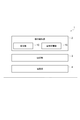
- FIG. 1 is a block diagram of the photodetector according to this embodiment.
- FIG. 2 is a schematic configuration diagram of the photodetector.
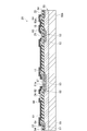
- FIG. 3 is a schematic cross-sectional view of the light detection unit.
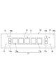
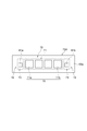
- FIG. 4 is a schematic plan view of the semiconductor substrate.
- FIG. 5 is a graph of data showing the relationship between the bias voltage applied to the APD and the gain of the APD to which the bias voltage is applied.
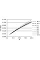
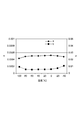
- FIG. 6 is a graph showing the temperature dependence of the slope and intercept of the regression line.
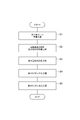
- FIG. 7 is a flowchart showing a method for manufacturing a semiconductor substrate.
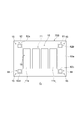
- FIG. 8 is a schematic plan view of a semiconductor substrate according to a modified example of this embodiment.
- FIG. 9 is a schematic plan view of a semiconductor substrate according to a modified example of this embodiment.
- FIG. 10 is a schematic plan view of a semiconductor substrate according to a modified example of this embodiment.
- FIG. 11 is a schematic plan view of a semiconductor substrate according to a modified example of this embodiment.
- FIG. 12 is a schematic plan view of a semiconductor substrate according to a modified example of this embodiment.
- FIG. 1 is a block diagram of the photodetector.
- the photodetection device 1 includes a detection operation unit 2, a circuit unit 3, and a power supply unit 4.
- the detection operation unit 2 has a light receiving unit 10 and a temperature compensation unit 15.
- the light receiving unit 10 has at least one APD.
- the APD of the light receiving unit 10 is an avalanche photodiode that operates in the linear mode.
- the temperature compensation unit 15 performs temperature compensation of the gain in the APD of the light receiving unit 10.
- the temperature compensation unit 15 controls the bias voltage applied to the APD of the light receiving unit 10.
- the temperature compensator 15 has a plurality of temperature compensating diodes for compensating the temperature of the gain of the APD.
- the circuit unit 3 applies a voltage to the light receiving unit 10 and the temperature compensating unit 15 of the detection operation unit 2.
- the circuit section 3 is electrically connected to each electrode of the APD of the light receiving section 10 and the temperature compensating diode of the temperature compensating section 15.
- the circuit unit 3 applies a voltage that causes the temperature compensating diode included in the temperature compensating unit 15 to be in the breakdown state to the APD of the light receiving unit 10.
- the power supply unit 4 generates an electromotive force that operates the detection operation unit 2.
- the power supply unit 4 applies a potential to the APD of the light receiving unit 10 and the temperature compensating diode of the temperature compensating unit 15 in the detecting operation unit 2 via the circuit unit 3.
- the power supply unit 4 brings the temperature compensating diode included in the temperature compensating unit 15 into a breakdown state.
- a voltage corresponding to the breakdown voltage is applied to the APD of the light receiving unit 10 as a bias voltage.
- the temperature compensating diode and the APD have the same temperature characteristic with respect to the relationship between the gain and the bias voltage.
- the breakdown voltage applied to the temperature compensating diode changes. Due to the change in the breakdown voltage applied to the temperature compensating diode, the bias voltage applied to the APD also changes according to the environmental temperature so that the gain of the APD is maintained. That is, the temperature compensation unit 15 performs temperature compensation of the gain in the APD of the light receiving unit 10.
- the photodetector 1 includes a photodetector 20, an electromotive force generator 31, a current limiter 32, a bias voltage stabilizer 33, and a setting unit 40.
- FIG. 2 is a schematic configuration diagram of the photodetector.
- the light detection unit 20 includes the light receiving unit 10 and the temperature compensation unit 15 described above.
- the electromotive force generator 31 generates an electromotive force that operates the photodetector 20.
- the current limiter 32 limits the current flowing through the photodetector 20.
- the bias voltage stabilizing unit 33 enables a current output equal to or higher than the upper limit value limited by the current limiting unit 32.
- the setting unit 40 controls the operation of the light detection unit 20.
- a part of the light detection unit 20 is included in the detection operation unit 2.
- a part of the light detection unit 20, the bias voltage stabilization unit 33, and the setting unit 40 are included in the circuit unit 3.
- the electromotive force generator 31 and the current limiter 32 are included in the power supply unit 4.
- the photodetector 20 includes, in addition to the light receiver 10 and the temperature compensator 15, a wiring part 21 that electrically connects the temperature compensator 15 and the light receiver 10, and a plurality of wiring parts 21. It has terminals 22, 23, 24, and 25.
- the terminal 22 is a first terminal and the plurality of terminals 25 are a plurality of second terminals.
- “electrically connected” and “electrically connected” also include a configuration in which a path is temporarily cut by a switch or the like.
- the light receiving unit 10 and the temperature compensation unit 15 are included in the detection operation unit 2.
- the wiring section 21 and the plurality of terminals 22, 23, 24, 25 are included in the circuit section 3.
- the plurality of temperature compensating diodes of the temperature compensating unit 15 are composed of a plurality of groups that are divided according to the difference in the voltage that is in the breakdown state at the same environmental temperature.
- the plurality of temperature compensating diodes of the temperature compensating unit 15 are composed of two groups 16 and 17.
- Each group 16, 17 includes at least one temperature compensating diode.
- the temperature compensating diodes in the same group are in a breakdown state at the same voltage at the same environmental temperature.
- the "same voltage" means that they are manufactured with the intention of being in a breakdown state at the same voltage. Therefore, the range of manufacturing error based on the above intention is also included.
- the voltage applied to the temperature compensating diode when the temperature compensating diodes 16a, 16b, 17a, 17b are in the breakdown state Is called “breakdown voltage”.
- breakdown voltage the voltage applied to the APD when the APD 11 is in the breakdown state.
- the temperature compensating unit 15 includes four temperature compensating diodes 16a, 16b, 17a, 17b as a plurality of temperature compensating diodes.
- the temperature compensating diodes 16a and 16b are included in the group 16, and the temperature compensating diodes 17a and 17b are included in the group 17.
- the light receiving unit 10 includes a plurality of APDs 11.
- the plurality of APDs 11 and the plurality of temperature compensating diodes 16a, 16b, 17a, 17b are included in the detection operation unit 2.
- the temperature compensating diode 16a is a first temperature compensating diode
- the temperature compensating diode 16b is a second temperature compensating diode
- the temperature compensating diode 17a is a third temperature compensating diode
- the temperature compensating diode 17b is a fourth temperature compensating diode.
- a plurality of APDs 11 have the same breakdown voltage.
- the temperature compensating diodes 16a and 16b have the same breakdown voltage.
- the temperature compensating diodes 17a and 17b have the same breakdown voltage.
- the temperature compensating diodes 16a and 16b of the group 16 and the temperature compensating diodes 17a and 17b of the group 17 have different breakdown voltages.
- the temperature compensating diode 16a and the temperature compensating diode 16b have a breakdown voltage at a voltage higher than that of the temperature compensating diode 17a and the temperature compensating diode 17b.
- the breakdown voltage of each temperature compensating diode 16a, 16b, 17a, 17b is lower than the breakdown voltage of any of the plurality of APDs 11.
- Each APD 11 has a pair of electrodes 19a and 19b.
- Each temperature compensating diode 16a, 16b, 17a, 17b has a pair of electrodes 29a, 29b.
- the electrodes 19a of the plurality of APDs 11 are connected to each other.
- the electrodes 19b of the plurality of APDs 11 are connected to each other.
- the electrodes 19b of the plurality of APDs 11 and the electrodes 29a of the plurality of temperature compensating diodes 16a, 16b, 17a, 17b are connected to each other.
- the electrode 29b of the temperature compensating diode 16a and the electrode 29b of the temperature compensating diode 16b are connected to each other.
- the electrode 29b of the temperature compensating diode 17a and the electrode 29b of the temperature compensating diode 17b are connected to each other. That is, the electrodes 29b of the temperature compensating diodes included in the same group are connected to each other.
- the wiring part 21 connects the electrode 19a of each APD 11 and the electrode 29a of each temperature compensation diode 16a, 16b, 17a, 17b in parallel to both the terminal 22 and the terminal 23.
- the wiring section 21 applies a voltage corresponding to the breakdown voltage of each temperature compensating diode 16a, 16b, 17a, 17b to each APD 11 as a bias voltage.
- the terminal 22 is electrically connected to the electrode 19 a of each APD 11, the electrodes 29 a of the temperature compensating diodes 16 a, 16 b, 17 a, and 17 b, and the current limiting unit 32 of the power supply unit 4. That is, the terminal 22 electrically connects the electrode 19a of each APD 11 and the electrode 29a of each temperature compensation diode 16a, 16b, 17a, 17b in parallel.
- the terminal 23 is electrically connected to the electrode 19a of each APD 11, the electrodes 29a of the temperature compensating diodes 16a, 16b, 17a, and 17b, and the bias voltage stabilizing unit 33.
- the terminal 24 is electrically connected to the electrode 19b of each APD 11 and a signal reading circuit (not shown).
- the plurality of terminals 25 are electrically connected to the electrodes 29b of the temperature compensating diodes 16a, 16b, 17a, 17b and the setting unit 40. Each terminal 25 is connected to the electrodes 29b of the temperature compensating diodes 16a, 16b, 17a, 17b different from each other.
- the electrode 19a is the anode of the APD 11
- the electrode 19b is the cathode of the APD 11.
- the electrode 29a is the anode of each temperature compensation diode 16a, 16b, 17a, 17b
- the electrode 29b is the cathode of each temperature compensation diode 16a, 16b, 17a, 17b.
- the electromotive force generation unit 31 and the current limiting unit 32 apply a voltage to the photodetection unit 20.
- the electromotive force generator 31 and the current limiter 32 are electrically connected to the terminal 22.
- the positive electrode of the electromotive force generation unit 31 is connected to the ground 36, and the negative electrode of the electromotive force generation unit 31 is connected to the terminal 22 via the current limiting unit 32.
- the bias voltage stabilizing unit 33 increases the upper limit value of the detection signal output from the APD 11.
- the bias voltage stabilizing unit 33 is connected in parallel with the current limiting unit 32 with respect to the photodetecting unit 20 and the electromotive force generating unit 31.
- the bias voltage stabilizing unit 33 is, for example, a capacitor.
- one electrode of the capacitor is connected to the negative electrode of the electromotive force generator 31, and the other electrode is connected to the terminal 23.
- the setting unit 40 sets the temperature compensation unit 15 according to the gain set in the APD 11.
- the setting unit 40 selects a group to be operated among the groups 16 and 17 of the plurality of temperature compensating diodes 16a, 16b, 17a and 17b.
- the setting unit 40 sets the group of temperature compensating diodes used for controlling the bias voltage from the group 16 of plural temperature compensating diodes 16a, 16b, 17a, 17b.
- the setting unit 40 sets the temperature compensating diodes to be operated by controlling the energization state of the plurality of temperature compensating diodes 16a, 16b, 17a, 17b.
- the setting unit 40 has at least one switch 41. At least one switch 41 is connected to the corresponding terminal 25. In the present embodiment, the setting unit 40 has two switches 41. One switch 41 is electrically connected to the temperature compensating diodes 16a and 16b of the group 16 through the corresponding terminals 25. The other switch 41 is electrically connected to the temperature compensating diodes 17a and 17b of the group 17 through the corresponding terminals 25. The switch 41 switches between a state in which the corresponding temperature compensation diodes 16a, 16b, 17a, 17b can be energized and a state in which they cannot be energized. The setting unit 40 controls ON/OFF of the switch 41. As a modified example of the present embodiment, the setting unit 40 may include four switches 41 corresponding to the temperature compensating diodes 16a, 16b, 17a, 17b.
- the light detection unit 20 has two terminals 25.
- the temperature compensating diodes 16a and 16b of the group 16 are connected to the same one terminal 25.
- the temperature compensating diodes 17a and 17b of the group 17 are connected to the same one terminal 25.
- the terminal 25 connected to the temperature compensating diodes 16 a and 16 b is connected to the ground 47 via the switch 41.
- the terminal 25 connected to the temperature compensating diodes 17 a and 17 b is connected to the ground 48 via the switch 41.
- the terminal 25 connected to the temperature compensating diodes 16a and 16b may be directly connected to the ground.
- FIG. 3 is a schematic cross-sectional view of the light detection unit.
- the light detection unit 20 is an optical member including a semiconductor substrate 50, as shown in FIG.
- the semiconductor substrate 50 has main surfaces 50a and 50b facing each other.
- the APD 11 and the temperature compensating diodes 16a, 16b, 17a, 17b are formed on the semiconductor substrate 50 so as to be separated from each other when viewed from the direction orthogonal to the main surface 50a.
- the APD 11 has a light incident surface 51a on the main surface 50a side.
- the temperature compensating diodes 16a, 16b, 17a, 17b are light-shielded APDs.
- the semiconductor substrate 50 includes a semiconductor region 51 and semiconductor layers 52, 53, 54 and 55.
- the APD 11 and the temperature compensating diodes 16a, 16b, 17a, 17b include a semiconductor region 51 and semiconductor layers 52, 53, 55, respectively.
- the semiconductor region 51 and the semiconductor layers 53, 54, 55 are of the first conductivity type, and the semiconductor layer 52 is of the second conductivity type.
- the semiconductor impurities are added by, for example, a diffusion method or an ion implantation method.
- the first conductivity type is P type and the second conductivity type is N type.
- a group 13 element such as B is used as the P-type impurity
- a group 15 element such as N, P, or As is used as the N-type impurity.
- the semiconductor region 51 is located on the main surface 50a side of the semiconductor substrate 50.
- the semiconductor region 51 constitutes a part of the main surface 50a.
- the semiconductor region 51 is, for example, P ⁇ type.
- the semiconductor layer 52 constitutes a part of the main surface 50a.
- the semiconductor layer 52 is in contact with the semiconductor region 51 and is surrounded by the semiconductor region 51 when viewed from the direction orthogonal to the main surface 50 a.
- the semiconductor layer 52 is, for example, N + type.
- the semiconductor layer 52 constitutes a cathode in each of the APD 11 and each of the temperature compensating diodes 16a, 16b, 17a, 17b.
- the semiconductor layer 53 is located between the semiconductor region 51 and the semiconductor layer 52. In other words, the semiconductor layer 53 is in contact with the semiconductor layer 52 on the main surface 50a side and is in contact with the semiconductor region 51 on the main surface 50b side.
- the semiconductor layer 53 has a higher impurity concentration than the semiconductor region 51.
- the semiconductor layer 53 is, for example, P-type.
- the impurity concentration of the semiconductor layer 53 of each temperature compensation diode 16a, 16b, 17a, 17b is higher than the impurity concentration of the semiconductor layer 53 of the APD 11.
- the semiconductor layer 53 constitutes an avalanche region in each of the APD 11 and each of the temperature compensation diodes 16a, 16b, 17a, 17b.
- the impurity concentration of the semiconductor layer 53 of the temperature compensating diodes 17a and 17b of the group 17 is higher than the impurity concentration of the semiconductor layer 53 of the temperature compensating diodes 16a and 16b of the group 16.
- the semiconductor layer 54 constitutes a part of the main surface 50a.
- the semiconductor layer 54 is in contact with the semiconductor region 51 and is surrounded by the semiconductor region 51 when viewed from the direction orthogonal to the main surface 50 a.
- the semiconductor layer 54 has a higher impurity concentration than the semiconductor region 51 and the semiconductor layer 53.
- the semiconductor layer 54 is, for example, a P + type.
- the semiconductor layer 54 is connected to the semiconductor layer 55 at a portion not shown.
- the semiconductor layer 54 constitutes the anode of the photodetector 1.
- the semiconductor layer 54 constitutes, for example, the APD 11 and the anodes of the temperature compensating diodes 16a, 16b, 17a, and 17b.
- the semiconductor layer 55 is located closer to the main surface 50b side of the semiconductor substrate 50 than the semiconductor region 51.
- the semiconductor layer 55 constitutes the entire main surface 50b.
- the semiconductor layer 55 is in contact with the semiconductor region 51 on the main surface 50a side.
- the semiconductor layer 55 has a higher impurity concentration than the semiconductor region 51 and the semiconductor layer 53.
- the semiconductor layer 55 is, for example, a P + type.
- the semiconductor layer 55 constitutes the anode of the photodetector 1.
- the semiconductor layer 55 constitutes, for example, the anodes of the APD 11 and the temperature compensating diodes 16a, 16b, 17a, 17b.
- the photodetector 1 further includes an insulating film 61, electrodes 62, 63, 64, a passivation film 66, and an antireflection film 67, which are provided on the main surface 50 a of the semiconductor substrate 50.
- the insulating film 61 is laminated on the main surface 50a of the semiconductor substrate 50.
- the insulating film 61 is, for example, a silicon oxide film.
- the electrodes 62, 63, 64 are arranged on the insulating film 61, respectively.
- the passivation film 66 is laminated on the insulating film 61 and the electrodes 62, 63, 64.
- the antireflection film 67 is laminated on the main surface 50a of the semiconductor substrate 50.
- the electrode 62 penetrates the insulating film 61 and is connected to the semiconductor layer 52 of the APD 11. A part of the electrode 62 is exposed from the passivation film 66 and constitutes the terminal 24 of the APD 11. The electrode 62 outputs the signal from the APD 11 at the terminal 24.
- the electrode 63 penetrates the insulating film 61 and is connected to the semiconductor layer 52 of each of the temperature compensating diodes 16a, 16b, 17a, 17b. A part of the electrode 63 is exposed from the passivation film 66 and constitutes the terminal 25 of each of the temperature compensating diodes 16a, 16b, 17a, 17b.
- the electrode 64 penetrates the insulating film 61 and is connected to the semiconductor layer 54. That is, the electrode 64 is connected to the APD 11 and each temperature compensation diode 16a, 16b, 17a, 17b. In other words, the APD 11 and the temperature compensating diodes 16a, 16b, 17a, 17b are connected to the electrode 64 in parallel with each other. A part of the electrode 64 is exposed from the passivation film 66 and constitutes, for example, the terminal 22.
- the terminal 24 is a pad electrode for the cathode of the APD 11.
- the terminal 25 is a pad electrode for the cathode of the temperature compensating diodes 16a, 16b, 17a, 17b.
- the terminal 22 is a pad electrode for the anode of the APD 11 and each of the temperature compensating diodes 16a, 16b, 17a, 17b.
- the terminal 22 is connected to the APD 11 and the temperature compensating diodes 16a, 16b, 17a and 17b in parallel with each other.
- a positive voltage is applied to the cathode pad electrode and a negative voltage is applied to the anode pad electrode.
- the antireflection film 67 is laminated on the semiconductor layer 52 of the APD 11. A part of the antireflection film 67 is exposed from the passivation film 66. Therefore, the light transmitted through the antireflection film 67 may enter the semiconductor layer 52 of the APD 11.
- the semiconductor layer 52 of each of the temperature compensating diodes 16a, 16b, 17a, 17b is covered with an insulating film 61 and shielded from light.
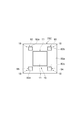
- FIG. 4 is a schematic plan view of the semiconductor substrate 50.
- the light detection unit 20 has a light detection region 71 in which the light receiving unit 10 is provided and a plurality of temperature detection regions 72 and 73 in which the temperature compensation unit 15 is provided. There is.
- the temperature detection areas 72 and 73 are located around the light detection area 71.
- the light detection area 71 is sandwiched between a temperature detection area 72 and a temperature detection area 73.
- the light detection area 71 is located between the temperature detection area 72 and the temperature detection area 73.
- the temperature detection area 72 is a first temperature detection area and the temperature detection area 73 is a second temperature detection area.
- At least one APD 11 is provided in the light detection area 71.
- the light receiving unit 10 includes five square APDs 11 as the plurality of APDs 11.
- the APD 11 may include four or less APDs, or may include six or more APDs.
- the plurality of APDs 11 are arranged in a line in the light detection area 71.
- the APD 11a is located at one end of the row and the APD 11b is located at the other end.
- the temperature detection area 72 is provided with at least one of the plurality of temperature compensating diodes 16a, 16b, 17a, 17b.
- the temperature detection area 73 is provided with the rest of the plurality of temperature compensation diodes 16a, 16b, 17a, 17b provided in the temperature detection area 72.
- the temperature detection region 72 is provided with temperature compensating diodes 16a and 17a.
- the temperature detection area 73 is provided with temperature compensating diodes 16b and 17b. That is, temperature compensating diodes of different groups 16 and 17 are provided in each of the temperature detecting regions 72 and 73.
- the plurality of temperature compensating diodes of the temperature compensating unit 15 are composed of three or more groups having different breakdown voltages, and the temperature compensating diodes of the three or more different groups have different temperatures. It may be provided in the detection areas 72 and 73.
- the temperature detection areas 72 and 73 are located along the arrangement direction of the plurality of APDs 11.
- the temperature detection area 72 is closest to the APD 11a among the plurality of APDs 11.
- the temperature detection area 73 is closest to the APD 11b among the plurality of APDs 11.
- the temperature compensating diodes 16a and 17a are arranged in a direction intersecting with the arrangement direction of the plurality of APDs 11 when viewed from the direction orthogonal to the main surface 50a.
- the temperature compensating diodes 16b and 17b are arranged in a direction intersecting with the arrangement direction of the plurality of APDs 11 when viewed from the direction orthogonal to the main surface 50a.
- the temperature compensating diodes 16a, 16b, 17a, 17b of the temperature compensating unit 15 and the APD 11 have the same temperature characteristic with respect to the relationship between the gain and the bias voltage.
- a voltage corresponding to the breakdown voltage of each temperature compensation diode 16a, 16b, 17a, 17b is applied to the APD 11 as a bias voltage.
- the temperature compensating unit 15 controls the bias voltage so that the difference voltage between the breakdown voltage of the APD 11 and the bias voltage applied to the APD 11 becomes constant.
- This differential voltage is determined as follows.
- FIG. 5 is a graph of data showing the relationship between the bias voltage applied to the APD and the gain of the APD to which the bias voltage is applied.
- FIG. 5 shows data at eight environmental temperatures of 100° C., 80° C., 60° C., 40° C., 20° C., 0° C., ⁇ 20° C., and ⁇ 40° C.
- FIG. 6 is a graph showing the temperature dependence of the slope “a” and the intercept “b” of the obtained regression line.
- the horizontal axis represents the environmental temperature and the vertical axis represents the values of “a” and “b”.
- the solid line shows the data of "a”
- the broken line shows the data of "b”.
- data indicating the relationship between the bias voltage applied to the APD and the gain of the APD to which the bias voltage is applied is acquired at an arbitrary temperature.
- the slope of the regression line with “(1/M) ⁇ (dM/dV r )” as the objective variable and “M” as the explanatory variable is given as “a” in equation (4), and the regression line
- the desired gain set in the APD 11 is substituted into “b” of the equation (4), and the intercept of “ 1 ” is substituted into the “M d ”of the equation (4).
- “ ⁇ V” is calculated.
- the temperature compensation unit 15 controls the bias voltage applied to the APD 11 so that the difference voltage becomes “ ⁇ V” calculated.
- the acquired data indicating the relationship between the bias voltage and the gain may not be the data of the APD of the same individual as the APD 11 as long as it is the APD having the same material and structure as the APD 11.
- the differential voltage is a subtraction value obtained by subtracting the voltage according to the breakdown voltage of the temperature compensating diodes 16a, 16b, 17a, 17b in the breakdown state from the breakdown voltage of the APD 11.
- a voltage corresponding to the breakdown voltage of the temperature compensating diodes 16a, 16b, 17a, 17b in the breakdown state is applied to the APD 11 as a bias voltage.
- the APD 11, the temperature compensating diodes 16a and 16b of the group 16 and the temperature compensating diodes 17a and 17b of the group 17 have different breakdown voltages.
- the impurity concentration of the semiconductor layer 53 of the temperature compensating diodes 16a, 16b, 17a, 17b and the impurity concentration of the semiconductor layer 53 of the APD 11, the breakdown voltage of the APD 11 and the temperature compensating diodes 16a, 16b, The difference voltage from the breakdown voltage of 17a and 17b is adjusted.
- the differential voltage may be adjusted depending on the circuit configuration. The differential voltage may be adjusted by applying an external voltage to the terminal 25.
- the breakdown voltage of the APD 11 may be the same as the breakdown voltage of the temperature compensating diodes 16a, 16b or the temperature compensating diodes 17a, 17b.
- the impurity concentration of the semiconductor layer 53 of each temperature compensation diode 16a, 16b, 17a, 17b is higher than that of the semiconductor layer 53 of the APD 11.
- the breakdown voltage of the APD 11 is higher than the breakdown voltage of each of the temperature compensating diodes 16a, 16b, 17a, 17b by " ⁇ V".
- the temperature compensating diodes 16a and 16b of the group 16 and the temperature compensating diodes 17a and 17b of the group 17 are designed to obtain different gains.
- “ ⁇ V” is calculated for each of the groups 16 and 17 of the temperature compensating diodes 16a, 16b, 17a and 17b by the equation (4), and the temperature compensating diodes 16a and 16b are calculated according to the calculated “ ⁇ V”.
- the impurity concentration of the semiconductor layer 53 of 17a and 17b is designed.
- the breakdown voltage of the temperature compensating diodes 16a, 16b, 17a, 17b is applied, so that the breakdown voltage is applied to the APD 11 as a bias voltage.
- one of the breakdown voltages of the plurality of temperature compensating diodes 16a, 16b, 17a, 17b is applied to the APD 11 as a bias voltage.
- the setting unit 40 controls which of the breakdown voltages of the temperature compensation diodes 16a and 16b and the temperature compensation diodes 17a and 17b is applied as a bias voltage to the APD 11.
- the terminal 22 is connected to the P + type semiconductor layer 54, and the semiconductor layer 54 is connected to the P + type semiconductor layer 55. Therefore, the anodes of the APD 11 and the temperature compensating diodes 16a, 16b, 17a, 17b are connected to the terminal 22 in parallel with each other. As a result, a negative potential is applied by the power supply unit 4 to the anodes of the APD 11 and the temperature compensating diodes 16a, 16b, 17a, 17b.
- the circuit unit 3 sets any one of the temperature compensating diodes 16a, 16b, 17a, and 17b in the breakdown state.
- the setting unit 40 selects a group to be operated from the plurality of groups 16 and 17 with the switch 41.
- the setting unit 40 switches the switch 41 on and off to select a group of temperature compensating diodes to which the breakdown voltage is applied as a bias voltage to the APD 11.
- the setting unit 40 sets a plurality of temperature compensating diodes 16a, 16b, 17a so that “ ⁇ V” calculated by substituting the gain set in the APD 11 into “M d ”in the equation (4) becomes a differential voltage.
- 17b a group used for controlling the bias voltage is selected from the groups 16 and 17.
- the breakdown voltage of the temperature compensating diode of the selected group is the potential difference between the potential applied to the terminal 25 corresponding to the temperature compensating diode and the potential applied to the terminal 22. Therefore, a potential according to the breakdown voltage of the temperature compensating diodes of the selected group is applied to the anode of the APD 11. As a result, a voltage according to the breakdown voltage of the temperature compensating diodes of the selected group is applied to the APD 11 as a bias voltage.
- the setting unit 40 sets all the temperature compensating diodes 16a, 16b, 17a and 17b to the energizable state. That is, the setting unit 40 turns on all the switches 41 connected to the plurality of terminals 25. In this case, among the temperature compensating diodes 16a, 16b, 17a, 17b in the energizable state, since the temperature compensating diodes 17a, 17b of the group 17 have the smallest breakdown voltage, the temperature compensating group of the group 17 is compensated. The diodes 17a and 17b operate. That is, the breakdown voltage of the temperature compensating diodes 17a and 17b is applied to the APD 11 as a bias voltage.
- the setting unit 40 When operating the temperature compensating diodes 16a and 16b of the group 16, the setting unit 40 sets the temperature compensating diodes 16a and 16b of the group 16 to an energizable state, and turns on the temperature compensating diodes 17a and 17b of the group 17. Turn off the power.
- the setting unit 40 turns on the switch 41 connected to the terminal 25 corresponding to the group 16 and turns off the switch 41 connected to the terminal 25 corresponding to the group 17.
- the breakdown voltage of the temperature compensating diodes 16a and 16b of the group 16 is applied to the APD 11 as a bias voltage.
- the gain of the APD 11 is selected by the setting unit 40.
- the setting unit 40 sets the temperature compensating diodes 16a and 16b of the group 16 to the energizable state regardless of whether or not the temperature compensating diodes 17a and 17b of the group 17 are energizable. To do.
- the group 17 is selected as the group of temperature compensation diodes to be operated by the setting unit 40.
- the combination of the electromotive force generator 31 and the current limiter 32 is connected to the terminal 22 so that the breakdown voltage of the temperature compensating diodes 17a and 17b of the group 17 selected in the terminal 22 is applied.
- the output voltage of the electromotive force generator 31 is equal to or higher than the operating voltage of the APD 11.
- the output voltage of the electromotive force generator 31 is equal to or higher than the upper limit of the temperature fluctuation of the breakdown voltage of each temperature compensation diode 16a, 16b, 17a, 17b.
- the output voltage of the electromotive force generator 31 is 300 V or higher.
- the current limiting unit 32 is composed of, for example, a current mirror circuit or a resistor.
- the gain of the APD 11 can be set arbitrarily according to the breakdown voltage difference between the temperature compensating diodes 17a and 17b of the selected group 17 and the APD 11. If the gain of the APD 11 is set to the optimum multiplication factor Mopt having a high S/N ratio, the detection accuracy can be improved.
- the anodes of the APD 11 and the temperature compensating diodes 16a, 16b, 17a, 17b are integrally formed by the semiconductor layer 55.
- the anode of the APD 11 is A potential of -130V is applied to the. Therefore, when the breakdown voltage of the APD 11 is 150 V under the environmental temperature of 25° C., the APD 11 operates in a state where the potential difference between the anode and the cathode is 20 V lower than the breakdown voltage.
- the APD 11 and the temperature compensating diodes 16a, 16b, 17a, and 17b have the same temperature characteristics with respect to the relationship between the gain and the bias voltage. Therefore, as long as the temperature compensating diodes 17a and 17b of the selected group 17 are in the breakdown state, the APD 11 receives a bias voltage 20 V lower than the breakdown voltage under the environmental temperature of 25° C. It operates by maintaining the gain of. In other words, in the photodetection device 1, the voltage that brings the temperature compensating diodes 17a and 17b of the selected group 17 into the breakdown state is applied to the temperature compensating diodes 17a and 17b, so that the gain of the APD 11 is reduced. Temperature compensation is realized.
- the function and effect of the photodetector in the above-described embodiment and modification will be described.
- a photodetector including an APD and a temperature compensating diode having the same temperature characteristics an inspection for selecting and combining APDs having a desired temperature characteristic with respect to the relationship between gain and bias voltage. was needed. Therefore, it is difficult to reduce the cost.
- the APD 11 and the temperature compensating diodes 16a, 16b, 17a, 17b are formed on the same semiconductor substrate 50, respectively.
- the temperature characteristics of the gain and the bias voltage in the wide temperature range are easily and highly accurately compared with the case where the temperature compensating diodes 16a, 16b, 17a, 17b and the APD 11 are formed on different semiconductor substrates. Equivalent temperature compensating diodes 16a, 16b, 17a, 17b and APD 11 are formed. Therefore, temperature compensation for the gain of the APD 11 can be realized while suppressing the manufacturing cost.
- the semiconductor substrate 50 includes a semiconductor region 51 of the first conductivity type.
- the APD 11 and each of the temperature compensating diodes 16a, 16b, 17a, 17b include a semiconductor layer 52 and a semiconductor layer 53, respectively.
- the semiconductor layer 52 is of the second conductivity type.
- the semiconductor layer 53 is of the first conductivity type having a higher impurity concentration than the semiconductor region 51.
- the semiconductor layer 53 is located between the semiconductor region 51 and the semiconductor layer 52.
- the temperature compensating diodes 16a, 16b, 17a, and 17b have the same configuration as the APD 11. Therefore, it is possible to easily form a plurality of temperature compensating diodes 16a, 16b, 17a, 17b whose temperature characteristics regarding gain and bias voltage are very similar to those of the APD 11.
- the impurity concentration in the semiconductor layer 53 of each temperature compensation diode 16a, 16b, 17a, 17b is higher than the impurity concentration in the semiconductor layer 53 of the APD 11.
- the breakdown voltage of the APD 11 is higher than the breakdown voltage of each of the temperature compensating diodes 16a, 16b, 17a, 17b.
- the semiconductor substrate 50 has a lower impurity concentration in the semiconductor layer 53 of the temperature compensating diodes 16a, 16b, 17a, 17b than in the semiconductor layer 53 of the APD 11. Is configured to be.
- the breakdown voltage of the APD 11 is smaller than the breakdown voltage of each of the temperature compensating diodes 16a, 16b, 17a, 17b.
- the slope of the regression line with “(1/M) ⁇ (dM/dV r )” as the objective variable and “M” as the explanatory variable is expressed as “a” in Equation (4) and the intercept is calculated as By substituting it into “b” in (4), the above-mentioned differential voltage with which a desired gain is obtained is determined. Therefore, a desired gain can be obtained extremely easily without strictly considering the environmental temperature.
- the temperature compensating unit 15 has temperature compensating diodes 16a, 16b, 17a, 17b.
- the temperature compensator 15 applies a voltage corresponding to the breakdown voltage applied to any one of the temperature compensating diodes 16a, 16b, 17a, 17b to the APD 11 as a bias voltage.
- the differential voltage is a subtraction value obtained by subtracting the voltage corresponding to the breakdown voltage of the temperature compensating diode 17a from the breakdown voltage of the APD 11. Therefore, the impurity concentration of the APD 11 and the temperature compensating diodes 16a, 16b, 17a, and 17b can be designed so that " ⁇ V" with which a desired gain can be obtained is derived and the subtraction value becomes " ⁇ V".
- the photodetector 1 includes a setting unit 40 and a wiring unit 21.
- the setting unit 40 sets the temperature compensating unit 15 according to the gain set in the APD 11.
- the wiring part 21 electrically connects the temperature compensating part 15 and the APD 11.
- the plurality of temperature compensating diodes 16a, 16b, 17a, 17b have different breakdown voltages.
- the wiring part 21 applies a voltage corresponding to the breakdown voltage of each of the temperature compensating diodes 16a, 16b, 17a, 17b to the APD 11 as a bias voltage.
- the setting unit 40 sets a plurality of temperature compensating diodes 16a, 16b, 17a so that “ ⁇ V” calculated by substituting the gain set in the APD 11 into “M d ”in the equation (4) becomes a differential voltage. , 17b to set the temperature compensation diode used for controlling the bias voltage. Therefore, the setting unit 40 sets the temperature compensating diode used for controlling the bias voltage from the plurality of temperature compensating diodes 16a, 16b, 17a, 17b. Therefore, it is possible to extremely easily obtain a desired gain according to the situation without strictly considering the environmental temperature. In other words, the desired gain can be easily switched, and the desired gain can be stably obtained at temperature.
- the circuit unit 3 electrically connects the APD 11 and the temperature compensating diodes 16a, 16b, 17a, 17b to the terminal 22 in parallel.
- the breakdown voltage of the temperature compensating diode in the breakdown state becomes a bias voltage for the APD 11. Is applied.
- the differential voltage between the breakdown voltage of the APD 11 and the bias voltage applied to the APD 11 is set, and the APD 11 has a gain according to the differential voltage. Therefore, depending on the temperature compensating diode that is brought into the breakdown state, the APD 11 can stably obtain a desired gain according to the situation.
- the circuit unit 3 has at least one switch 41.
- the switch 41 is electrically connected to the corresponding temperature compensating diodes 16a, 16b, 17a, 17b.
- the switch 41 switches between a state in which the corresponding temperature compensation diodes 16a, 16b, 17a, 17b can be energized and a state in which they cannot be energized.
- the temperature compensating diodes 16a and 16b have a higher breakdown voltage than the temperature compensating diodes 17a and 17b.
- the switch 41 is electrically connected to the temperature compensating diodes 17a and 17b.
- the temperature compensating diodes 17a and 17b are turned on by the switch 41, the temperature compensating diodes 17a and 17b are prioritized even if the temperature compensating diodes 16a and 16b are on. And breaks down. Thus, the desired gain can be switched in the APD 11 according to the situation with easy control.
- At least one switch 41 is connected to the corresponding terminal 25.
- a high voltage is applied between the electrodes 29a of the temperature compensating diodes 16a, 16b, 17a, 17b and the APD 11. Therefore, easier control can be achieved by electrically connecting the switch 41 to the electrode 29b through the terminal 25 than by arranging the switch 41 between the electrode 29a and the APD 11.
- the circuit unit 3 sets the temperature compensating diodes 16a and 16b to be energizable regardless of whether or not the temperature compensating diodes 17a and 17b are energizable. In this case, even if all of the temperature compensating diodes 17a and 17b are damaged, the temperature compensating diodes 16a and 16b are in a breakdown state. Therefore, a large current is prevented from flowing to the APD 11, and the photodetector 1 is prevented from malfunctioning.
- the temperature detection area 72 and the temperature detection area 73 where the plurality of temperature compensating cords 16a, 16b, 17a, 17b are provided are located with the light detection area 71 in between. Therefore, even if the temperature locally rises near the temperature detection region 72, the temperature compensating diodes 16b and 17b provided in the temperature detection region 73 can operate normally. That is, the photodetection device 1 has improved resistance to local temperature changes.
- the temperature compensator 15 includes temperature compensating diodes 16a and 16b having the same breakdown voltage as a plurality of temperature compensating diodes.
- the temperature compensating diode 16a is provided in the temperature detection region 72.
- the temperature compensation diode 16b is provided in the temperature detection region 73. Therefore, even if the temperature is locally high near the temperature detection region 72 and the temperature compensation diode 16a does not function normally, the temperature compensation diode 16b provided in the temperature detection region 73 can operate normally. Therefore, a stable bias voltage can be applied to the APD 11 even if the temperature locally changes. Therefore, the desired gain can be stably obtained in the APD 11.
- the temperature compensating unit 15 includes, as a plurality of temperature compensating diodes, temperature compensating diodes 17a and 17b having different breakdown voltages from the temperature compensating diodes 16a and 16b.
- the temperature compensating diodes 17a and 17b have the same breakdown voltage.
- the temperature compensating diode 17a is provided in the temperature detecting region 72.
- the temperature compensation diode 17b is provided in the temperature detection region 73. In this case, the voltage applied as the bias voltage to the APD 11 can be switched between the breakdown voltage of the temperature compensating diodes 17a and 17b and the breakdown voltage of the temperature compensating diodes 16a and 16b.
- the temperature compensation diodes 16b and 17b provided in the temperature detection region 73 are It can work normally. Therefore, a stable and desired bias voltage can be applied to the APD 11 even if the temperature locally changes. Therefore, a desired gain according to the situation can be stably obtained in the APD 11.
- the light detection unit 20 has a plurality of APDs 11 as at least one APD 11.
- a plurality of APDs 11 are provided in the light detection area 71. In this case, a temperature difference is likely to occur around the photo detection area 71 in which the APD 11 is provided.
- the photodetection device 1 since the temperature detection region 72 and the temperature detection region 73 are located with the photodetection region 71 in between, resistance to local temperature change is improved.
- FIG. 7 is a flowchart showing a method for manufacturing the semiconductor substrate 50 of the photodetector 1.
- a semiconductor wafer is prepared (step S1).
- the semiconductor wafer is a substrate before being processed as the semiconductor substrate 50, and has main surfaces 50a and 50b facing each other.
- the semiconductor wafer includes a first conductivity type semiconductor region corresponding to the semiconductor region 51.
- the semiconductor region is provided on the main surface 50a side of the semiconductor wafer and constitutes the entire main surface 50a.
- the semiconductor region of a semiconductor wafer is P ⁇ type.
- a semiconductor layer 55 of the first conductivity type having a higher impurity concentration than the semiconductor region of the semiconductor wafer is formed in the semiconductor wafer by adding impurities from the main surface 50b side.
- the semiconductor layer 55 is a P + type.
- the determination method is as follows.
- step S2 the slope of the regression line with “(1/M) ⁇ (dM/dV r )” as the objective variable and “M” as the explanatory variable in the data showing the correlation between the bias voltage applied to the APD and the gain of the APD.
- V r is a bias voltage applied to the APD
- M is a gain of the APD to which the bias voltage is applied.
- the data used in step S2 is a separate body made of the same material and structure as APD11.
- the above-mentioned difference voltage with which a desired gain is obtained is determined using the acquisition result in step S2 and the equation (4) (step S3).
- the obtained slope is used as “a” in equation (4)
- the obtained intercept is used as “b” in equation (4)
- the desired gain to be set in the APD 11 is given in equation (4). It corresponds to “ ⁇ V” calculated by substituting for “M d ”.
- a plurality of mutually different values are determined as the gain set in the APD 11, and a plurality of differential voltages are determined for these values.
- a plurality of “ ⁇ V” calculated by substituting a plurality of different values into “M d ”of the equation (4) is determined as the difference voltage corresponding to each of the plurality of values.
- a first ion implantation step impurity ions are implanted into the main surface 50a side by an ion implantation method to add impurities, whereby the second conductivity type semiconductor layer 52 and the first conductivity type are formed.
- the semiconductor layers 53 and 54 of the mold are formed.
- the semiconductor layer 52 is N + type
- the semiconductor layer 53 is P type
- the semiconductor layer 54 is P + type.
- the semiconductor layer 52 is formed by implanting impurity ions of the second conductivity type into different locations separated from each other in one ion implantation process.
- the semiconductor layer 53 is formed by implanting impurity ions of the first conductivity type after the semiconductor layer 52 is formed.
- the semiconductor layer 53 may be formed by implanting impurity ions of the first conductivity type before the semiconductor layer 52 is formed.
- the semiconductor layers 52 and 53 are formed at positions overlapping with each other when viewed from the direction orthogonal to the main surface 50a.
- the semiconductor layer 53 is formed by implanting an impurity of the first conductivity type at a position deeper than the semiconductor layer 52 when viewed from the main surface 50a side.
- the semiconductor layers 52 and 53 are formed in a plurality of locations separated from each other when viewed from a direction orthogonal to the main surface 50a in a region that becomes one semiconductor substrate 50.
- the plurality of places include a place where the APD 11 is arranged and a place where the temperature compensating diodes 16a, 16b, 17a, 17b are arranged.
- the second conductivity type impurity is added to each part so that the semiconductor layer 52 has the same impurity concentration.
- the first conductivity type impurities are added to the respective portions so that the semiconductor layers 53 have the same impurity concentration.
- step S5 impurities are further added only to the semiconductor layer 53 at some of the plurality of locations described above by the ion implantation method.
- the first conductivity type impurity is further implanted into the semiconductor layer 53 only at the locations where the temperature compensating diodes 16a, 16b, 17a and 17b are arranged. Therefore, in the photodetector 1, the impurity concentration in the semiconductor layer 53 of each of the temperature compensation diodes 16a, 16b, 17a, 17b is higher than the impurity concentration in the semiconductor layer 53 of the APD 11.
- the photodetector 1 is configured such that the breakdown voltage of the APD 11 is higher than the breakdown voltage of each of the temperature compensating diodes 16a, 16b, 17a, 17b.
- the amount of the first conductivity type impurity implanted into the semiconductor layer 53 of each temperature compensation diode 16a, 16b, 17a, 17b in steps S4 and S5 depends on the differential voltage determined in step S3.
- the amount of the first conductivity type impurity implanted into the semiconductor layer 53 of the temperature compensating diodes 17a and 17b is the same as the amount of the first conductivity type impurity implanted into the semiconductor layer 53 of the temperature compensating diodes 16a and 16b. Greater than the amount of impurities.
- the breakdown voltage of the temperature compensating diodes 16a and 16b is configured to be higher than the breakdown voltage of the temperature compensating diodes 17a and 17b.
- the first conductivity type impurity is further implanted into the semiconductor layer 53 only at the location where the APD 11 is disposed, not at the location where the temperature compensation diodes 16a, 16b, 17a, and 17b are disposed. Good.
- the impurity concentration in the semiconductor layer 53 of each of the temperature compensating diodes 16a, 16b, 17a, 17b is lower than the impurity concentration in the semiconductor layer 53 of the APD 11.
- the breakdown voltage of the APD 11 is configured to be smaller than the breakdown voltage of each of the temperature compensating diodes 16a, 16b, 17a, 17b.
- the semiconductor substrate 50 of the photodetector 1 is formed by the above steps. Steps S2 and S3 may be performed before step S1 or after step S4. In the present embodiment, the semiconductor layers 52, 53, 54 are formed from the state where the semiconductor layer 55 is already formed. However, the semiconductor layer 55 may be formed after the semiconductor layers 52, 53, 54 are formed.
- the semiconductor layer 52 and the semiconductor layer 53 are formed at each of the locations by implanting ions at different locations. After that, ions are further implanted into the semiconductor layer 53 at some positions. Therefore, it is possible to easily manufacture the plurality of temperature compensating diodes 16a, 16b, 17a, 17b and the APD 11 that have the same temperature characteristics with respect to the gain and the bias voltage and are set to desired breakdown voltages. In this case, the gain of the APD 11 can be arbitrarily set according to the difference voltage between the breakdown voltage of each of the temperature compensation diodes 16a, 16b, 17a, 17b and the breakdown voltage of the APD 11.
- the detection accuracy can be improved. For example, if the gain of the APD 11 is set to the optimum multiplication factor Mopt having a high S/N ratio according to the difference voltage, the detection accuracy can be improved. As described above, in the above-described manufacturing method, temperature compensation for the gain of the APD 11 is realized while suppressing the manufacturing cost, and the detection accuracy is improved.
- the slope and intercept of the regression line with “(1/M) ⁇ (dM/dV r )” as the objective variable and “M” as the explanatory variable are acquired.
- the obtained slope into “a” of the equation (4)
- the obtained intercept into “b” of the equation (4)
- the differential voltage with which a desired gain is obtained is determined. Therefore, the above-mentioned differential voltage with which a desired gain is obtained can be determined very easily without strictly considering the environmental temperature.
- a plurality of “ ⁇ V” calculated by substituting a plurality of mutually different values as gains set in the APD 11 into “M d ”of the equation (4) corresponds to each of the plurality of values. Is determined as the differential voltage to be applied. Therefore, the plurality of difference voltages corresponding to the plurality of values can be determined very easily without strictly considering the environmental temperature.
- the photodetector 1 may have a configuration in which the reverse APD 11 operates in the linear mode.
- the photodetector 1 may have a configuration in which the reach-through type APD 11 operates in the Geiger mode.
- the photodetector 1 may have a configuration in which the reverse APD 11 operates in Geiger mode.
- a quenching resistor is connected to the APD 11, and the impurity concentration of the semiconductor layer 53 of the temperature compensating diodes 16a, 16b, 17a, 17b is higher than that of the semiconductor layer 53 of the APD 11.
- the semiconductor substrate 50 is configured to be low.
- the photodetection device 1 having the electromotive force generating unit 31, the current limiting unit 32, the bias voltage stabilizing unit 33, and the setting unit 40 has been described.
- the photodetector according to the present embodiment may have a configuration that does not include at least one of the electromotive force generator 31, the current limiter 32, the bias voltage stabilizer 33, and the setting unit 40.
- an external device connected to the photodetector may function as the electromotive force generator 31, the current limiter 32, the bias voltage stabilizer 33, or the setting unit 40.
- the photodetector 1 may include a signal read circuit (not shown).
- the configuration has been described in which the switch 41 is connected to the terminal 25 of the light detection unit 20 and the switch 41 is controlled by the setting unit 40.
- the switch 41 may be arranged inside the light detection unit 20.
- the terminals 22, 23, 24, 25 have been described as pad electrodes.
- the terminals 22, 23, 24, 25 may be made of the semiconductor in the semiconductor substrate 50.
- the switch 41 for switching the electrical connection between the temperature compensating diodes 16a, 16b, 17a, 17b and the APD 11 is arranged in the wiring section 21 and the setting section 40 controls ON/OFF of the switch 41 in the wiring section 21. Good. Also in this case, the setting unit 40 controls the bias voltage applied to the APD 11. Since a high voltage is applied between the APD 11 and each of the temperature compensating diodes 16a, 16b, 17a, 17b, the switch 41 connected to the terminal 25 is more than the case where the switch arranged in the wiring section 21 is controlled. Is easier to control.
- the temperature compensator 15 may include a plurality of temperature compensating diodes having the same breakdown voltage. According to this configuration, even if a part of the temperature compensating diode is damaged or a local temperature change occurs in the vicinity of where the part of the temperature compensating diode is arranged, the photodetection device 1 does not normally operate. The operation can be realized.
- FIG. 8 is a schematic plan view of a semiconductor substrate 70A according to a modified example of this embodiment.
- FIG. 9 is a schematic plan view of a semiconductor substrate 70B in a modified example of this embodiment.
- FIG. 10 is a schematic plan view of a semiconductor substrate 70C in a modified example of this embodiment.
- FIG. 11 is a schematic plan view of a semiconductor substrate 70D according to a modified example of this embodiment.
- FIG. 12 is a schematic plan view of a semiconductor substrate 70E according to a modified example of this embodiment.
- the semiconductor substrates 70A, 70B, 70C, 70D and 70E respectively correspond to the semiconductor substrate 50 of the above-described embodiment. These variations are generally similar or the same as the embodiments described above. These modified examples differ from the above-described embodiment in the positional relationship between the plurality of temperature compensating diodes in the temperature compensating unit 15 and the APD 11 included in the light receiving unit 10. Hereinafter, differences from the above-described embodiment will be mainly described.
- the modification shown in FIG. 8 is generally similar or the same as the above-described embodiment.
- This modified example is different from the above-described embodiment in the number of temperature compensating diodes in the temperature compensating unit 15 and the number of APDs 11 included in the light receiving unit 10.
- differences from the above-described embodiment will be mainly described.
- the light receiving unit 10 has four APDs 11.
- the temperature compensator 15 includes temperature compensating diodes 81a and 81b.
- the temperature compensating diodes 81a and 81b have the same breakdown voltage. That is, in this modification, the plurality of temperature compensating diodes of the temperature compensating unit 15 are composed of only one group having the same breakdown voltage.
- the temperature compensating diode 81a is a first temperature compensating diode
- the temperature compensating diode 81b is a second temperature compensating diode.
- a plurality of temperature compensating diodes 81a and 81b are provided in the temperature detecting areas 72 and 73.
- the temperature detection area 72 is provided with a temperature compensation diode 81a.
- a temperature compensating diode 81b is provided in the temperature detecting region 73.
- the temperature compensating diodes 81a and 81b are arranged in the arrangement direction of the plurality of APDs 11.
- the modification shown in FIG. 9 is generally similar or the same as the modification shown in FIG.
- This modified example is different from the modified example shown in FIG. 8 with respect to the number and position of temperature compensating diodes in the temperature compensating unit 15 and the shape of the APD 11 included in the light receiving unit 10.
- differences from the modification shown in FIG. 8 will be mainly described.
- the photodetecting section 20 includes a photodetecting area 71 in which the light receiving section 10 is provided and a plurality of temperature detecting areas 92, 93, 94, 95 in which the temperature compensating section 15 is provided. And have.
- the temperature detection areas 92, 93, 94, 95 are located around the light detection area 71.
- the temperature detection areas 92, 93, 94, 95 are located on all sides of the light detection area 71.
- the light detection area 71 is sandwiched between a temperature detection area 92 and a temperature detection area 94. In other words, the light detection area 71 is located between the temperature detection area 92 and the temperature detection area 94.
- the light detection area 71 is sandwiched between a temperature detection area 93 and a temperature detection area 95. In other words, the light detection area 71 is located between the temperature detection area 93 and the temperature detection area 95.
- the light receiving unit 10 has four APDs 11.
- the four APDs 11 are provided in the light detection area 71.
- four APDs 11 are arranged in a line in the light detection area 71.
- the APD 11a is located at one end of the row and the APD 11b is located at the other end.
- Each of the four APDs 11 has a shape extending in a direction intersecting the arrangement direction of the four APDs 11 when viewed from a direction orthogonal to the main surface 50a.
- Each APD 11 has a rectangular shape whose short side is the arrangement direction when viewed from the direction orthogonal to the main surface 50a.
- the temperature detection areas 92 and 95 are closest to the APD 11a among the plurality of APDs 11.
- the temperature detection areas 93 and 94 are closest to the APD 11b among the plurality of APDs 11.
- the temperature compensator 15 includes temperature compensating diodes 82a, 82b, 82c, 82d.
- the temperature compensating diodes 82a, 82b, 82c, 82d have the same breakdown voltage. Temperature compensating diodes 82a, 82b, 82c, 82d are provided in each of the temperature detecting regions 92, 93, 94, 95.
- the temperature detection area 92 is provided with a temperature compensating diode 82a.
- a temperature compensating diode 82b is provided in the temperature detecting region 93.
- a temperature compensating diode 82c is provided in the temperature detecting region 94.
- a temperature compensating diode 82d is provided in the temperature detecting region 95.
- the present modification shown in FIG. 10 is generally similar or the same as the modification shown in FIG. This modification is different from the modification shown in FIG. 9 in the number and shape of the APDs 11 included in the light receiving unit 10.
- differences from the modification shown in FIG. 9 will be mainly described.
- the light receiving unit 10 has one square APD 11.
- This one square APD 11 is provided in the light detection area 71.
- the temperature detection areas 92, 93, 94, and 95 are arranged close to the four corners of the square APD 11, respectively. That is, the temperature compensating diodes 82a, 82b, 82c, 82d are arranged close to the four corners of the square APD 11, respectively.
- Each side of the APD 11 in the modification shown in FIG. 10 is longer than the short side of the APD 11 in the modification shown in FIG.
- Each side of the APD 11 in the modification shown in FIG. 10 is 10 times or more the side of each of the temperature compensating diodes 82a, 82b, 82c, 82d.
- One APD 11 is provided in the light detection area 71.
- the modification shown in FIG. 11 is generally similar to or the same as the modification shown in FIGS. 9 and 10.
- This modified example is different from the modified examples shown in FIGS. 9 and 10 in the number and shape of the APDs 11 included in the light receiving unit 10.
- differences from the modifications shown in FIGS. 9 and 10 will be mainly described.
- the light receiving unit 10 has a plurality of APDs 11 arranged in a matrix when viewed from the direction orthogonal to the main surface 50a.
- the light receiving unit 10 has 16 APDs 11 arranged in 4 rows and 4 columns. These 16 APDs 11 are arranged in the light detection area 71.
- the temperature detection areas 92, 93, 94, and 95 are arranged close to the APDs 11 located at the four corners of the APDs 11 arranged in a matrix. That is, the temperature compensating diodes 82a, 82b, 82c, 82d are arranged close to the APDs 11 located at the four corners of the APDs 11 arranged in a matrix.
- the modification shown in FIG. 12 is generally similar or the same as the modification shown in FIG. 11. This modification is different from the modification shown in FIG. 11 with respect to the number and positions of the temperature compensating diodes included in each of the temperature detection regions 92, 93, 94, and 95. Hereinafter, differences from the modification shown in FIG. 11 will be mainly described.
- a plurality of temperature compensating diodes having different breakdown voltages are provided in each of the plurality of temperature detecting regions.
- four temperature compensating diodes are provided in each of the temperature detecting areas 92, 93, 94, and 95.
- the four temperature compensation diodes have different breakdown voltages. That is, in this modification, the plurality of temperature compensating diodes of the temperature compensating unit 15 are composed of four groups having different breakdown voltages. In each of the temperature detecting regions 92, 93, 94, 95, the four temperature compensating diodes are arranged in a matrix of 2 rows and 2 columns.
- the temperature detection region 92 is provided with temperature compensating diodes 82a, 83a, 84a, 85a having different breakdown voltages.
- the temperature detection region 93 is provided with temperature compensating diodes 82b, 83b, 84b, 85b having different breakdown voltages.
- the temperature detection region 94 is provided with temperature compensating diodes 82c, 83c, 84c, 85c having different breakdown voltages.
- temperature compensating diodes 82d, 83d, 84d, 85d having different breakdown voltages are provided. As described in the modification shown in FIG. 9, the temperature compensating diodes 82a, 82b, 82c, 82d have the same breakdown voltage.
- the temperature compensating diodes 83a, 83b, 83c, 83d have the same breakdown voltage.
- the temperature compensating diodes 84a, 84b, 84c, 84d have the same breakdown voltage.
- the temperature compensating diodes 85a, 85b, 85c, 85d have the same breakdown voltage.
Landscapes
- Physics & Mathematics (AREA)
- General Physics & Mathematics (AREA)
- Spectroscopy & Molecular Physics (AREA)
- Light Receiving Elements (AREA)
- Solid State Image Pick-Up Elements (AREA)
- Photometry And Measurement Of Optical Pulse Characteristics (AREA)
Abstract
Selon l'invention, un dispositif (1) de détection optique comporte une unité (20) de détection optique. L'unité (20) de détection optique possède: une photodiode à avalanche (PDA) (11); plusieurs diodes (16a, 16b, 17a, 17b) pour compensation de la chaleur; et des bornes (22) qui relient électriquement en parallèle la PDA (11) et les diodes (16a, 16b, 17a, 17b) pour compensation de la chaleur. Les diodes (16a, 16b, 17a, 17b) pour compensation de la chaleur effectuent une compensation de la chaleur du gain de la PDA (11). L'unité (20) de détection optique possède une région (71) de détection optique et des régions (72, 73) de détection de la température. La PDA (11) est située dans la région (71) de détection optique. Les régions (72, 73) de détection de la température sont situées sur la circonférence de la région (71) de détection optique. Les diodes (16a, 16b, 17a, 17b) pour compensation de la chaleur sont situées dans les régions (72, 73) de détection de la température. La région (71) de détection optique est située entre la région (72) de détection de la température et la région (73) de détection de la température.
Priority Applications (3)
| Application Number | Priority Date | Filing Date | Title |
|---|---|---|---|
| US17/311,763 US11927478B2 (en) | 2018-12-12 | 2019-11-29 | Light detection device |
| EP19895340.8A EP3988907B1 (fr) | 2018-12-12 | 2019-11-29 | Dispositif de détection optique |
| CN201980057018.6A CN113167641B (zh) | 2018-12-12 | 2019-11-29 | 光检测装置 |
Applications Claiming Priority (6)
| Application Number | Priority Date | Filing Date | Title |
|---|---|---|---|
| JP2018-232892 | 2018-12-12 | ||
| JP2018232892 | 2018-12-12 | ||
| JP2018232895 | 2018-12-12 | ||
| JP2018-232895 | 2018-12-12 | ||
| JP2019175948A JP6681509B1 (ja) | 2018-12-12 | 2019-09-26 | 光検出装置 |
| JP2019-175948 | 2019-09-26 |
Publications (1)
| Publication Number | Publication Date |
|---|---|
| WO2020121859A1 true WO2020121859A1 (fr) | 2020-06-18 |
Family
ID=70166526
Family Applications (2)
| Application Number | Title | Priority Date | Filing Date |
|---|---|---|---|
| PCT/JP2019/046909 Ceased WO2020121859A1 (fr) | 2018-12-12 | 2019-11-29 | Dispositif de détection optique |
| PCT/JP2019/046901 Ceased WO2020121855A1 (fr) | 2018-12-12 | 2019-11-29 | Procédé de détermination et dispositif de détection de lumière |
Family Applications After (1)
| Application Number | Title | Priority Date | Filing Date |
|---|---|---|---|
| PCT/JP2019/046901 Ceased WO2020121855A1 (fr) | 2018-12-12 | 2019-11-29 | Procédé de détermination et dispositif de détection de lumière |
Country Status (8)
| Country | Link |
|---|---|
| US (2) | US11927478B2 (fr) |
| EP (3) | EP3988907B1 (fr) |
| JP (5) | JP7454917B2 (fr) |
| KR (2) | KR102778754B1 (fr) |
| CN (5) | CN113167637B (fr) |
| DE (2) | DE112019006173T5 (fr) |
| TW (1) | TWI851628B (fr) |
| WO (2) | WO2020121859A1 (fr) |
Families Citing this family (10)
| Publication number | Priority date | Publication date | Assignee | Title |
|---|---|---|---|---|
| JPWO2020121857A1 (ja) * | 2018-12-12 | 2021-11-04 | 浜松ホトニクス株式会社 | 光検出装置及び光検出装置の製造方法 |
| US12080822B2 (en) | 2018-12-12 | 2024-09-03 | Hamamatsu Photonics K.K. | Photodetector and method for manufacturing photodetector |
| US12113088B2 (en) | 2018-12-12 | 2024-10-08 | Hamamatsu Photonics K.K. | Light detection device |
| US11901379B2 (en) * | 2018-12-12 | 2024-02-13 | Hamamatsu Photonics K.K. | Photodetector |
| JP7454917B2 (ja) | 2018-12-12 | 2024-03-25 | 浜松ホトニクス株式会社 | 光検出装置 |
| JP7739108B2 (ja) * | 2020-10-14 | 2025-09-16 | キヤノン株式会社 | 光電変換装置、光検出システム及び移動体 |
| JP7721275B2 (ja) | 2021-01-22 | 2025-08-12 | キヤノン株式会社 | 半導体素子、機器、チップ |
| CN117501149A (zh) * | 2021-06-21 | 2024-02-02 | 索尼半导体解决方案公司 | 光接收元件 |
| JP7675572B2 (ja) * | 2021-06-23 | 2025-05-13 | 浜松ホトニクス株式会社 | アバランシェフォトダイオードアレイ |
| WO2026079604A1 (fr) * | 2024-10-10 | 2026-04-16 | 엘지이노텍 주식회사 | Réseau de dispositifs de détection de lumière |
Citations (4)
| Publication number | Priority date | Publication date | Assignee | Title |
|---|---|---|---|---|
| JPS556924U (fr) * | 1978-06-27 | 1980-01-17 | ||
| JPH03278482A (ja) * | 1989-08-04 | 1991-12-10 | Canon Inc | 光電変換装置 |
| JPH0727607A (ja) | 1993-07-09 | 1995-01-31 | Hamamatsu Photonics Kk | アバランシェフォトダイオードのバイアス回路 |
| US20180180473A1 (en) * | 2016-12-22 | 2018-06-28 | Sick Ag | Light Receiver Having a Plurality of Avalanche Photodiode Elements and Method for Supplying a Bias Voltage |
Family Cites Families (79)
| Publication number | Priority date | Publication date | Assignee | Title |
|---|---|---|---|---|
| FR1582850A (fr) * | 1968-03-29 | 1969-10-10 | ||
| JPS5062389A (fr) | 1973-10-01 | 1975-05-28 | ||
| GB1535824A (en) | 1976-02-11 | 1978-12-13 | Standard Telephones Cables Ltd | Avalanche photodetector biassing system |
| GB1532262A (en) * | 1976-04-03 | 1978-11-15 | Ferranti Ltd | Photodiode circuit arrangements |
| US4181863A (en) * | 1976-04-03 | 1980-01-01 | Ferranti Limited | Photodiode circuit arrangements |
| GB1503088A (en) | 1976-07-22 | 1978-03-08 | Standard Telephones Cables Ltd | Avalanche photodetector |
| JPS5341280A (en) * | 1976-09-27 | 1978-04-14 | Nippon Telegr & Teleph Corp <Ntt> | Photodetecting system of multiplication constant control |
| JPS6017051B2 (ja) | 1978-11-20 | 1985-04-30 | 東京光学機械株式会社 | アバランシェ・ダイオ−ドの温度補償方法 |
| JPS55127082A (en) * | 1979-03-23 | 1980-10-01 | Nec Corp | Bias voltage generating circuit of avalanche photodiode |
| SE417145B (sv) | 1979-05-30 | 1981-02-23 | Asea Ab | Lavinfotodiodanordning med en lavindiod och med organ for styrning av diodens multiplikationsfaktor |
| US4464048A (en) | 1981-03-25 | 1984-08-07 | Barr & Stroud Limited | Laser rangefinders |
| JPS60178673A (ja) | 1984-02-24 | 1985-09-12 | Nec Corp | アバランシフオトダイオ−ド |
| JPS60180347A (ja) * | 1984-02-28 | 1985-09-14 | Fujitsu Ltd | アバランシエフオトダイオ−ドの温度補償回路 |
| JPS60211886A (ja) | 1984-04-05 | 1985-10-24 | Nec Corp | アバランシフオトダイオ−ドの製造方法 |
| JPS6138975U (ja) * | 1984-08-09 | 1986-03-11 | 株式会社東芝 | 印刷配線板 |
| JPH0799782B2 (ja) * | 1985-06-18 | 1995-10-25 | 株式会社ニコン | 半導体光検出装置 |
| JPS62239727A (ja) | 1986-04-11 | 1987-10-20 | Nec Corp | アバランシエホトダイオ−ドの利得制御方式 |
| JPS62279671A (ja) * | 1986-05-28 | 1987-12-04 | Mitsubishi Electric Corp | 固体撮像装置 |
| JPH0828488B2 (ja) * | 1987-07-07 | 1996-03-21 | 富士通株式会社 | 半導体装置 |
| JPH01118714A (ja) * | 1987-10-30 | 1989-05-11 | Omron Tateisi Electron Co | 光学式位置検出センサ |
| US4948989A (en) * | 1989-01-31 | 1990-08-14 | Science Applications International Corporation | Radiation-hardened temperature-compensated voltage reference |
| JPH0321082A (ja) * | 1989-06-19 | 1991-01-29 | Fujitsu Ltd | 光受信回路 |
| JPH04111477A (ja) * | 1990-08-31 | 1992-04-13 | Sumitomo Electric Ind Ltd | 受光素子 |
| JPH04256376A (ja) * | 1991-02-08 | 1992-09-11 | Hamamatsu Photonics Kk | アバランシェホトダイオード及びその製造方法 |
| JPH05235396A (ja) * | 1992-02-24 | 1993-09-10 | Sumitomo Electric Ind Ltd | 半導体受光装置 |
| JP3121100B2 (ja) | 1992-03-25 | 2000-12-25 | 株式会社日立製作所 | 固体撮像装置 |
| JPH06224463A (ja) | 1993-01-22 | 1994-08-12 | Mitsubishi Electric Corp | 半導体受光装置 |
| JPH0763854A (ja) * | 1993-06-16 | 1995-03-10 | Kansei Corp | レーザー送受光装置 |
| JP3421103B2 (ja) | 1993-12-20 | 2003-06-30 | 浜松ホトニクス株式会社 | アバランシェフォトダイオードを用いた光検出回路 |
| JPH07263653A (ja) | 1994-03-17 | 1995-10-13 | Hamamatsu Photonics Kk | 固体撮像装置 |
| JPH08207281A (ja) * | 1995-02-06 | 1996-08-13 | Canon Inc | インクジェット記録ヘッド |
| JPH10247717A (ja) * | 1997-03-04 | 1998-09-14 | Matsushita Electron Corp | 半導体装置 |
| JP3479966B2 (ja) * | 1998-01-30 | 2003-12-15 | 住友電気工業株式会社 | 光電流モニタ回路及び光受信器 |
| JPH11275755A (ja) * | 1998-03-19 | 1999-10-08 | Fujitsu Ltd | アバランシェフォトダイオード保護回路を有する光受信回路 |
| JP2000171295A (ja) | 1998-12-03 | 2000-06-23 | Nec Corp | Apdバイアス回路 |
| JP3668926B2 (ja) | 1999-08-27 | 2005-07-06 | 株式会社ルネサステクノロジ | 光インタコネクション受信モジュール |
| US6313459B1 (en) * | 2000-05-31 | 2001-11-06 | Nortel Networks Limited | Method for calibrating and operating an uncooled avalanche photodiode optical receiver |
| JP3509851B2 (ja) | 2000-12-28 | 2004-03-22 | サンケン電気株式会社 | 電子回路装置及びこれを使用したスィチング回路装置 |
| US20030117121A1 (en) * | 2001-12-20 | 2003-06-26 | Prescott Daniel C. | High-side current-sense circuit for precision application |
| KR100566197B1 (ko) | 2003-01-02 | 2006-03-29 | 삼성전자주식회사 | Apd 광수신기의 온도 보상 장치 |
| JP2004281488A (ja) | 2003-03-13 | 2004-10-07 | Renesas Technology Corp | 半導体装置及びその製造方法 |
| JP4223304B2 (ja) * | 2003-03-19 | 2009-02-12 | 三菱電機株式会社 | 光受信器 |
| JP2004303878A (ja) | 2003-03-31 | 2004-10-28 | Nippon Sheet Glass Co Ltd | 受光素子アレイ |
| JP3956923B2 (ja) * | 2003-09-19 | 2007-08-08 | 住友電気工業株式会社 | アバランシェフォトダイオードのバイアス電圧制御回路 |
| JP4399337B2 (ja) * | 2004-09-13 | 2010-01-13 | 株式会社フューチャービジョン | 平面パターンを有する基板およびそれを用いた表示装置 |
| JP2007266251A (ja) * | 2006-03-28 | 2007-10-11 | Nippon Telegr & Teleph Corp <Ntt> | 光半導体装置 |
| EP3002794B1 (fr) | 2006-07-03 | 2020-08-19 | Hamamatsu Photonics K.K. | Reseau de photodiodes |
| CN200950235Y (zh) | 2006-09-25 | 2007-09-19 | 深圳飞通光电子技术有限公司 | 雪崩光电二极管的温度补偿偏压电路 |
| CN200959101Y (zh) | 2006-10-12 | 2007-10-10 | 宁波中科集成电路设计中心有限公司 | 一种雪崩光电二极管的温度补偿装置 |
| JP4791334B2 (ja) | 2006-12-11 | 2011-10-12 | 富士通オプティカルコンポーネンツ株式会社 | 光受信装置および光受信装置のバイアス電圧制御方法 |
| JP4642047B2 (ja) | 2007-06-15 | 2011-03-02 | 三洋電機株式会社 | 半導体装置 |
| JP2009038157A (ja) | 2007-07-31 | 2009-02-19 | Sumitomo Electric Ind Ltd | 受光素子アレイ、一次元受光素子アレイおよび二次元受光素子アレイ |
| JP5483544B2 (ja) | 2009-10-21 | 2014-05-07 | 住友電工デバイス・イノベーション株式会社 | 半導体受光装置 |
| CN201601136U (zh) | 2010-01-13 | 2010-10-06 | 山东交通职业学院 | 一种用于激光接收电路的温度补偿电路 |
| US20120101614A1 (en) * | 2010-10-22 | 2012-04-26 | Allan Ghaemi | System and Method for Manufacturing Optical Network Components |
| JP5844580B2 (ja) | 2011-09-05 | 2016-01-20 | 浜松ホトニクス株式会社 | 固体撮像素子及び固体撮像素子の実装構造 |
| JP5926921B2 (ja) | 2011-10-21 | 2016-05-25 | 浜松ホトニクス株式会社 | 光検出装置 |
| JP5791461B2 (ja) * | 2011-10-21 | 2015-10-07 | 浜松ホトニクス株式会社 | 光検出装置 |
| JP2013164263A (ja) | 2012-02-09 | 2013-08-22 | Mitsubishi Electric Corp | 受光装置及び距離測定装置及び形状測定装置 |
| JP5984617B2 (ja) | 2012-10-18 | 2016-09-06 | 浜松ホトニクス株式会社 | フォトダイオードアレイ |
| DE102013100696B3 (de) * | 2013-01-24 | 2013-11-07 | Sick Ag | Optoelektronischer Sensor und Verfahren zur Erfassung von Objekten in einem Überwachungsbereich |
| KR101448393B1 (ko) * | 2013-06-27 | 2014-10-08 | 단국대학교 천안캠퍼스 산학협력단 | 의료용 레이저 수신단의 apd 이득 안정화 방법 |
| CN103728030A (zh) | 2013-12-20 | 2014-04-16 | 中国科学院合肥物质科学研究院 | Apd温度自适应近红外单光子探测装置 |
| US9541656B2 (en) * | 2013-12-20 | 2017-01-10 | General Electric Company | System and method for compensating temperature gain variation in radiation detectors |
| JP2016061729A (ja) | 2014-09-19 | 2016-04-25 | 株式会社東芝 | 光子検出素子、光子検出装置、及び放射線分析装置 |
| CN106033225B (zh) | 2015-03-16 | 2017-08-25 | 苏州旭创科技有限公司 | 低功耗apd偏压控制器与偏压控制方法及光电接收器 |
| US10203400B2 (en) * | 2015-07-31 | 2019-02-12 | Avago Technologies International Sales Pte. Limited | Optical measurement system incorporating ambient light component nullification |
| US9954124B1 (en) * | 2016-01-08 | 2018-04-24 | Board Of Trustees Of The University Of Alabama, For And On Behalf Of The University Of Alabama In Huntsville | Thermo-compensated silicon photo-multiplier with on-chip temperature sensor |
| US11374043B2 (en) | 2016-07-27 | 2022-06-28 | Hamamatsu Photonics K.K. | Photodetection device with matrix array of avalanche diodes |
| CA3051963A1 (fr) | 2017-01-30 | 2018-08-02 | Medibeacon Inc. | Procede de surveillance non invasive d'agent traceur fluorescent avec corrections de reflexion diffuse |
| JP6696695B2 (ja) | 2017-03-16 | 2020-05-20 | 株式会社東芝 | 光検出装置およびこれを用いた被写体検知システム |
| JP6741703B2 (ja) | 2017-03-31 | 2020-08-19 | 株式会社デンソー | 光検出器 |
| KR102544296B1 (ko) | 2018-09-13 | 2023-06-16 | 쑤저우 레킨 세미컨덕터 컴퍼니 리미티드 | 표면발광레이저 소자 및 이를 구비한 표면발광레이저 장치 |
| US12113088B2 (en) | 2018-12-12 | 2024-10-08 | Hamamatsu Photonics K.K. | Light detection device |
| US12080822B2 (en) | 2018-12-12 | 2024-09-03 | Hamamatsu Photonics K.K. | Photodetector and method for manufacturing photodetector |
| JP7454917B2 (ja) | 2018-12-12 | 2024-03-25 | 浜松ホトニクス株式会社 | 光検出装置 |
| JPWO2020121857A1 (ja) | 2018-12-12 | 2021-11-04 | 浜松ホトニクス株式会社 | 光検出装置及び光検出装置の製造方法 |
| US11513002B2 (en) * | 2018-12-12 | 2022-11-29 | Hamamatsu Photonics K.K. | Light detection device having temperature compensated gain in avalanche photodiode |
| US20230083263A1 (en) | 2021-09-15 | 2023-03-16 | Kabushiki Kaisha Toshiba | Light detector, light detection system, lidar device, and mobile body |
-
2019
- 2019-06-14 JP JP2019111528A patent/JP7454917B2/ja active Active
- 2019-06-14 JP JP2019111529A patent/JP7455520B2/ja active Active
- 2019-09-26 JP JP2019175941A patent/JP6681508B1/ja active Active
- 2019-09-26 JP JP2019175945A patent/JP7475123B2/ja active Active
- 2019-09-26 JP JP2019175948A patent/JP6681509B1/ja active Active
- 2019-11-29 DE DE112019006173.9T patent/DE112019006173T5/de active Pending
- 2019-11-29 CN CN201980081932.4A patent/CN113167637B/zh active Active
- 2019-11-29 CN CN201980081953.6A patent/CN113167638B/zh active Active
- 2019-11-29 KR KR1020217021020A patent/KR102778754B1/ko active Active
- 2019-11-29 US US17/311,763 patent/US11927478B2/en active Active
- 2019-11-29 CN CN201980082092.3A patent/CN113302462B/zh active Active
- 2019-11-29 EP EP19895340.8A patent/EP3988907B1/fr active Active
- 2019-11-29 US US17/311,766 patent/US11561131B2/en active Active
- 2019-11-29 EP EP19897484.2A patent/EP3896412B1/fr active Active
- 2019-11-29 WO PCT/JP2019/046909 patent/WO2020121859A1/fr not_active Ceased
- 2019-11-29 CN CN201980056994.XA patent/CN113167640B/zh active Active
- 2019-11-29 DE DE112019006185.2T patent/DE112019006185T5/de active Pending
- 2019-11-29 WO PCT/JP2019/046901 patent/WO2020121855A1/fr not_active Ceased
- 2019-11-29 EP EP19897203.6A patent/EP3988909B1/fr active Active
- 2019-11-29 KR KR1020217021021A patent/KR102778755B1/ko active Active
- 2019-11-29 CN CN201980057018.6A patent/CN113167641B/zh active Active
- 2019-12-06 TW TW108144638A patent/TWI851628B/zh active
Patent Citations (4)
| Publication number | Priority date | Publication date | Assignee | Title |
|---|---|---|---|---|
| JPS556924U (fr) * | 1978-06-27 | 1980-01-17 | ||
| JPH03278482A (ja) * | 1989-08-04 | 1991-12-10 | Canon Inc | 光電変換装置 |
| JPH0727607A (ja) | 1993-07-09 | 1995-01-31 | Hamamatsu Photonics Kk | アバランシェフォトダイオードのバイアス回路 |
| US20180180473A1 (en) * | 2016-12-22 | 2018-06-28 | Sick Ag | Light Receiver Having a Plurality of Avalanche Photodiode Elements and Method for Supplying a Bias Voltage |
Also Published As
Similar Documents
| Publication | Publication Date | Title |
|---|---|---|
| JP6681509B1 (ja) | 光検出装置 | |
| US11513002B2 (en) | Light detection device having temperature compensated gain in avalanche photodiode | |
| JP2024086953A (ja) | 光検出装置及び光検出装置の製造方法 | |
| US12322744B2 (en) | Photodetector and method for manufacturing photodetector | |
| US9899434B1 (en) | Light-receiving device having avalanche photodiodes of different types | |
| WO2022019189A1 (fr) | Dispositif de photodétection | |
| US12618948B2 (en) | Photodetection device |
Legal Events
| Date | Code | Title | Description |
|---|---|---|---|
| 121 | Ep: the epo has been informed by wipo that ep was designated in this application |
Ref document number: 19895340 Country of ref document: EP Kind code of ref document: A1 |
|
| NENP | Non-entry into the national phase |
Ref country code: DE |
|
| ENP | Entry into the national phase |
Ref document number: 2019895340 Country of ref document: EP Effective date: 20210712 |