WO2020121875A1 - 走査アンテナおよび走査アンテナの製造方法 - Google Patents
走査アンテナおよび走査アンテナの製造方法 Download PDFInfo
- Publication number
- WO2020121875A1 WO2020121875A1 PCT/JP2019/047065 JP2019047065W WO2020121875A1 WO 2020121875 A1 WO2020121875 A1 WO 2020121875A1 JP 2019047065 W JP2019047065 W JP 2019047065W WO 2020121875 A1 WO2020121875 A1 WO 2020121875A1
- Authority
- WO
- WIPO (PCT)
- Prior art keywords
- liquid crystal
- layer
- substrate
- region
- transmission
- Prior art date
- Legal status (The legal status is an assumption and is not a legal conclusion. Google has not performed a legal analysis and makes no representation as to the accuracy of the status listed.)
- Ceased
Links
Images


Classifications
-
- H—ELECTRICITY
- H01—ELECTRIC ELEMENTS
- H01Q—ANTENNAS, i.e. RADIO AERIALS
- H01Q3/00—Arrangements for changing or varying the orientation or the shape of the directional pattern of the waves radiated from an antenna or antenna system
- H01Q3/26—Arrangements for changing or varying the orientation or the shape of the directional pattern of the waves radiated from an antenna or antenna system varying the relative phase or relative amplitude of energisation between two or more active radiating elements; varying the distribution of energy across a radiating aperture
- H01Q3/30—Arrangements for changing or varying the orientation or the shape of the directional pattern of the waves radiated from an antenna or antenna system varying the relative phase or relative amplitude of energisation between two or more active radiating elements; varying the distribution of energy across a radiating aperture varying the relative phase between the radiating elements of an array
-
- H—ELECTRICITY
- H01—ELECTRIC ELEMENTS
- H01Q—ANTENNAS, i.e. RADIO AERIALS
- H01Q3/00—Arrangements for changing or varying the orientation or the shape of the directional pattern of the waves radiated from an antenna or antenna system
- H01Q3/44—Arrangements for changing or varying the orientation or the shape of the directional pattern of the waves radiated from an antenna or antenna system varying the electric or magnetic characteristics of reflecting, refracting, or diffracting devices associated with the radiating element
-
- G—PHYSICS
- G02—OPTICS
- G02F—OPTICAL DEVICES OR ARRANGEMENTS FOR THE CONTROL OF LIGHT BY MODIFICATION OF THE OPTICAL PROPERTIES OF THE MEDIA OF THE ELEMENTS INVOLVED THEREIN; NON-LINEAR OPTICS; FREQUENCY-CHANGING OF LIGHT; OPTICAL LOGIC ELEMENTS; OPTICAL ANALOGUE/DIGITAL CONVERTERS
- G02F1/00—Devices or arrangements for the control of the intensity, colour, phase, polarisation or direction of light arriving from an independent light source, e.g. switching, gating or modulating; Non-linear optics
- G02F1/01—Devices or arrangements for the control of the intensity, colour, phase, polarisation or direction of light arriving from an independent light source, e.g. switching, gating or modulating; Non-linear optics for the control of the intensity, phase, polarisation or colour
- G02F1/13—Devices or arrangements for the control of the intensity, colour, phase, polarisation or direction of light arriving from an independent light source, e.g. switching, gating or modulating; Non-linear optics for the control of the intensity, phase, polarisation or colour based on liquid crystals, e.g. single liquid crystal display cells
- G02F1/133—Constructional arrangements; Operation of liquid crystal cells; Circuit arrangements
- G02F1/1333—Constructional arrangements; Manufacturing methods
- G02F1/1339—Gaskets; Spacers; Sealing of cells
-
- H—ELECTRICITY
- H01—ELECTRIC ELEMENTS
- H01Q—ANTENNAS, i.e. RADIO AERIALS
- H01Q19/00—Combinations of primary active antenna elements and units with secondary devices, e.g. with quasi-optical devices, for giving the antenna a desired directional characteristic
- H01Q19/10—Combinations of primary active antenna elements and units with secondary devices, e.g. with quasi-optical devices, for giving the antenna a desired directional characteristic using reflecting surfaces
-
- H—ELECTRICITY
- H01—ELECTRIC ELEMENTS
- H01Q—ANTENNAS, i.e. RADIO AERIALS
- H01Q21/00—Antenna arrays or systems
- H01Q21/0006—Particular feeding systems
- H01Q21/0012—Radial guide fed arrays
-
- H—ELECTRICITY
- H01—ELECTRIC ELEMENTS
- H01Q—ANTENNAS, i.e. RADIO AERIALS
- H01Q9/00—Electrically-short antennas having dimensions not more than twice the operating wavelength and consisting of conductive active radiating elements
- H01Q9/04—Resonant antennas
- H01Q9/0407—Substantially flat resonant element parallel to ground plane, e.g. patch antenna
-
- H—ELECTRICITY
- H10—SEMICONDUCTOR DEVICES; ELECTRIC SOLID-STATE DEVICES NOT OTHERWISE PROVIDED FOR
- H10D—INORGANIC ELECTRIC SEMICONDUCTOR DEVICES
- H10D30/00—Field-effect transistors [FET]
- H10D30/60—Insulated-gate field-effect transistors [IGFET]
- H10D30/67—Thin-film transistors [TFT]
Definitions
- the present invention relates to a scanning antenna, and more particularly, to a scanning antenna in which an antenna unit (also referred to as “element antenna”) has a liquid crystal capacity (also referred to as “liquid crystal array antenna”) and manufacturing of such a scanning antenna. Regarding the method.
- an antenna unit also referred to as “element antenna”
- a liquid crystal capacity also referred to as “liquid crystal array antenna”
- Antennas for mobile communication and satellite broadcasting require the function of changing the beam direction (referred to as “beam scanning” or “beam steering”).
- beam scanning As an antenna having such a function (hereinafter, referred to as "scanned antenna"), a phased array antenna including an antenna unit is known.
- the conventional phased array antenna is expensive, which is an obstacle to its widespread use in consumer products. In particular, the cost increases significantly as the number of antenna units increases.
- Non-Patent Documents 1 to 5 scanning antennas utilizing the large dielectric anisotropy (birefringence) of liquid crystal materials (including nematic liquid crystals and polymer dispersed liquid crystals) have been proposed (Patent Documents 1 to 5 and Non-Patent Document 1). Since the dielectric constant of the liquid crystal material has frequency dispersion, in this specification, the dielectric constant in the microwave frequency band (also referred to as “dielectric constant for microwave”) is particularly “dielectric constant M ( ⁇ M )”. Will be written as.
- Patent Document 3 and Non-Patent Document 1 describe that a low-cost scanning antenna can be obtained by utilizing the technology of a liquid crystal display device (hereinafter, referred to as “LCD”).
- LCD liquid crystal display device
- Patent Document 6 by the applicant is a scanning antenna that can be mass-produced by using a conventional LCD manufacturing technique, a TFT substrate used for such a scanning antenna, and a manufacturing method and a driving method of such a scanning antenna. Is disclosed. For reference, the entire disclosure of Patent Document 6 is incorporated herein.
- Another object of the present invention is to further improve the performance of the scanning antenna described in Patent Document 6.
- a scanning antenna having a transmission/reception area including a plurality of antenna units, and a non-transmission/reception area outside the transmission/reception area,
- a TFT substrate having a first dielectric substrate and a plurality of TFTs, a plurality of gate bus lines, a plurality of source bus lines, and a plurality of patch electrodes supported by the first dielectric substrate;
- a second dielectric substrate and a slot electrode formed on the first main surface of the second dielectric substrate, the slot electrode having a plurality of slots arranged corresponding to the plurality of patch electrodes.
- a slot substrate having A liquid crystal layer provided between the TFT substrate and the slot substrate, A seal portion provided in the non-transmission/reception region and surrounding the liquid crystal layer, A reflective conductive plate arranged to face a second main surface of the second dielectric substrate opposite to the first main surface via a dielectric layer; A first spacer structure disposed in the transmission/reception region and defining a first gap between the first dielectric substrate and the second dielectric substrate in the transmission/reception region; A second spacer structure that defines a second gap between the first dielectric substrate and the second dielectric substrate in the non-transmission/reception region that is wider than the first gap, The scanning antenna, wherein the second spacer structure is disposed in the seal portion or in a region surrounded by the seal portion.
- the scanning antenna according to item 1 wherein when the temperature of the liquid crystal layer is 25° C., the liquid crystal layer has vacuum bubbles, and when the temperature of the liquid crystal layer is 120° C. or higher, the liquid crystal layer does not have vacuum bubbles. .
- the first spacer structure includes a first columnar spacer defining a thickness of the liquid crystal layer between the patch electrode and the slot electrode, 3.
- the scanning antenna according to item 1 or 2 wherein the second spacer structure includes a spacer higher than the first columnar spacer.
- the seal portion includes a first granular spacer that defines a thickness of the liquid crystal layer in the transmission/reception area, 4.
- the second spacer structure is arranged in the seal portion.
- a third spacer structure defining a third gap between the first dielectric substrate and the second dielectric substrate in the non-transmission/reception region, which is wider than the first gap, and is surrounded by the seal portion.
- a third spacer structure disposed in the region, The scanning antenna according to any one of Items 1 to 5, further comprising an additional seal portion including the third spacer structure.
- the additional seal portion When viewed from the normal direction of the first dielectric substrate, the additional seal portion is formed along a side having the largest notch from the rectangle when the smallest rectangle including the TFT substrate and the slot substrate is drawn. Item 7.
- [Item 8] 8 The scanning antenna according to item 6 or 7, wherein the height of the third spacer structure is larger than the height of the second spacer structure.
- the area surrounded by the seal portion has an active area including the transmission/reception area and a buffer area other than the active area, and the additional seal portion is provided between the active area and the buffer area.
- the seal part has a main seal part that defines an injection port, and an end seal part that seals the injection port, 10.
- Item 11 Item 11.
- the step of forming the liquid crystal layer includes: between the TFT substrate and the slot substrate and within a region surrounded by the seal portion.
- a method of manufacturing a scanning antenna comprising the step of supplying a liquid crystal material so as to generate vacuum bubbles in the substrate.
- the step of forming the liquid crystal layer further includes a step of raising the temperature of the liquid crystal layer to 120° C. or higher after the step of supplying the liquid crystal material.
- the liquid crystal layer is formed using a vacuum injection method.
- the liquid crystal layer is formed using a drop injection method, and the step of forming the liquid crystal layer is performed by using a liquid crystal material between the TFT substrate and the slot substrate and having a volume smaller than that of a region surrounded by the seal portion.
- the antenna performance of the scanning antenna can be further improved.
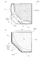
- FIG. (A) And (b) is a schematic plan view which shows the TFT substrate 101 and the slot substrate 201 with which the scanning antenna 1000 is equipped, respectively.
- (A)-(c) is a figure which shows the example of the tiling structure of the scanning antenna 1000.
- 3 is a schematic plan view of a liquid crystal panel 100a included in the scanning antenna 1000.
- FIG. (A)-(c) is a typical sectional view of the liquid crystal panel 100a.
- 1 is a schematic plan view of a liquid crystal panel 100Aa included in a scanning antenna according to Embodiment 1 of the present invention.
- (A)-(c) is a typical sectional view of liquid crystal panel 100Aa.
- FIG. 1 is a typical top view of liquid crystal panels 100Aa1-100Aa4 of a modification of liquid crystal panel 100Aa, respectively.
- (A) is a schematic plan view for explaining a position where the additional seal portion 76 is formed, and
- (b) is a schematic plan view of a liquid crystal panel 100Aa5 which is a modified example of the liquid crystal panel 100Aa.
- (A)-(e) is a schematic sectional view for explaining a manufacturing method of the TFT substrate 101Aa included in the scanning antenna according to the first embodiment of the present invention, and (f) is a schematic diagram showing the TFT substrate 101Aa.
- FIG. 1 is a schematic plan view for explaining a position where the additional seal portion 76 is formed
- (b) is a schematic plan view of a liquid crystal panel 100Aa5 which is a modified example of the liquid crystal panel 100Aa.
- (A)-(e) is a schematic sectional view for explaining a manufacturing method of the TFT substrate 101Aa included
- FIG. 3 is a cross-sectional view schematically showing the structure of a transfer part included in the TFT substrate 101Aa and the slot substrate 201Aa. It is a figure which shows typically the example of the spacer structure which the liquid crystal panel 100Aa has.
- FIG. 1 shows typically the example of the spacer structure which the liquid crystal panel 100Aa5 has.
- (A)-(e) is a typical sectional view for explaining the manufacturing method of TFT substrate 101B with which the scanning antenna by Embodiment 2 of the present invention is provided, and (f) is a schematic diagram showing TFT substrate 101B.
- FIG. (A)-(e) is a schematic sectional view for explaining a manufacturing method of the TFT substrate 101C included in the scanning antenna according to the third embodiment of the present invention, and (f) is a schematic diagram showing the TFT substrate 101C.
- FIG. (A)-(e) is a typical sectional view for explaining the manufacturing method of TFT substrate 101D with which the scanning antenna by Embodiment 4 of the present invention is provided, and (f) is a schematic diagram showing TFT substrate 101D.
- FIG. (A)-(e) is a schematic sectional view for explaining a manufacturing method of the TFT substrate 101E included in the scanning antenna according to the fifth embodiment of the present invention, and (f) is a schematic diagram showing the TFT substrate 101E.
- a scanning antenna, a method of manufacturing the scanning antenna, and a TFT substrate used for the scanning antenna according to an embodiment of the present invention will be described with reference to the drawings.
- the present invention is not limited to the embodiments exemplified below.
- the embodiment of the present invention is not limited to the drawings.
- the thickness of the layer in the cross-sectional view and the sizes of the conductive portion and the opening in the plan view are examples.
- a scanning antenna using an antenna unit that utilizes anisotropy (birefringence index) of a large dielectric constant M ( ⁇ M ) of a liquid crystal material is a voltage applied to each liquid crystal layer of the antenna unit associated with a pixel of an LCD panel. Control is performed to change the effective permittivity M ( ⁇ M ) of the liquid crystal layer of each antenna unit, thereby forming a two-dimensional pattern for each antenna unit having a different capacitance (for displaying an image on the LCD. Corresponding.).
- An electromagnetic wave for example, microwave
- emitted from the antenna or received by the antenna is given a phase difference according to the capacitance of each antenna unit, and is formed by the antenna units having different capacitances.
- Non-Patent Document 2 discloses a basic structure of a scanning antenna in which spiral slots are arranged. For reference, all the disclosures of Patent Documents 1 to 4 and Non-Patent Documents 1 and 2 are incorporated herein.
- the antenna unit of the scanning antenna is similar to the pixel of the LCD panel, it is different from the pixel structure of the LCD panel, and the arrangement of the plurality of antenna units is also different from the pixel array of the LCD panel.
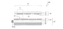
- a basic structure of a scanning antenna will be described with reference to FIG. 1 showing a scanning antenna 1000 described in Patent Document 6.
- the scanning antenna 1000 is a radial in-line slot antenna in which slots are arranged concentrically, but the scanning antenna according to the embodiment of the present invention is not limited to this.
- the slots are arranged in various known arrangements. Good.
- the entire disclosure of Patent Document 5 is incorporated herein by reference for the arrangement of slots and/or antenna units.
- FIG. 1 is a cross-sectional view schematically showing a part of the scanning antenna 1000, in which a feed pin 72 (see FIG. 2B) provided in the vicinity of the center of slots arranged concentrically extends along the radial direction. A part of the cross section is schematically shown.
- the scanning antenna 1000 includes a TFT substrate 101, a slot substrate 201, a liquid crystal layer LC disposed between them, a slot substrate 201, and a reflective conductive plate 65 disposed so as to face each other with an air layer 54 in between. Is equipped with.
- the scanning antenna 1000 transmits and receives microwaves from the TFT substrate 101 side.
- the TFT substrate 101 has a dielectric substrate 1 such as a glass substrate, a plurality of patch electrodes 15 formed on the dielectric substrate 1, and a plurality of TFTs 10. Each patch electrode 15 is connected to the corresponding TFT 10. Each TFT 10 is connected to a gate bus line and a source bus line.
- the slot substrate 201 has a dielectric substrate 51 such as a glass substrate and a slot electrode 55 formed on the liquid crystal layer LC side of the dielectric substrate 51.
- the slot electrode 55 has a plurality of slots 57.
- a reflective conductive plate 65 is arranged so as to face the slot substrate 201 via the air layer 54.
- a layer formed of a dielectric material for example, fluororesin such as PTFE
- the slot electrode 55, the reflective conductive plate 65, and the dielectric substrate 51 and the air layer 54 between them function as the waveguide 301.
- the patch electrode 15, the portion of the slot electrode 55 including the slot 57, and the liquid crystal layer LC between them form the antenna unit U.
- one patch electrode 15 faces the portion of the slot electrode 55 including one slot 57 via the liquid crystal layer LC and constitutes a liquid crystal capacitance.
- the structure in which the patch electrode 15 and the slot electrode 55 face each other via the liquid crystal layer LC is similar to the structure in which the pixel electrode of the LCD panel and the counter electrode face each other via the liquid crystal layer. That is, the antenna unit U of the scanning antenna 1000 and the pixel in the LCD panel have a similar structure. Further, the antenna unit has a configuration similar to that of the pixel in the LCD panel in that the antenna unit has an auxiliary capacitance electrically connected in parallel with the liquid crystal capacitance. However, the scanning antenna 1000 has many differences from the LCD panel.
- the performance required for the dielectric substrates 1 and 51 of the scanning antenna 1000 is different from the performance required for the LCD panel substrate.
- a substrate transparent to visible light is used for an LCD panel, for example, a glass substrate or a plastic substrate.
- a semiconductor substrate may be used because the substrate on the back side does not need to be transparent.
- the dielectric substrates 1 and 51 for the antenna have a small dielectric loss with respect to microwaves (the dielectric loss tangent with respect to microwaves is represented by tan ⁇ M ).
- the tan ⁇ M of the dielectric substrates 1 and 51 is preferably about 0.03 or less, more preferably 0.01 or less.
- a glass substrate or a plastic substrate can be used.
- the glass substrate has better dimensional stability and heat resistance than the plastic substrate, and is suitable for forming circuit elements such as TFTs, wirings and electrodes by using LCD technology.
- the material forming the waveguide is air and glass
- the dielectric loss of glass is larger, and thus the thinner the glass, the more the waveguide loss can be reduced.
- the conductive material used for the electrodes is also different.
- An ITO film is often used as a transparent conductive film for pixel electrodes and counter electrodes of LCD panels.
- ITO has a large tan ⁇ M against microwaves and cannot be used as a conductive layer in an antenna.
- the slot electrode 55 functions as a wall of the waveguide 301 together with the reflective conductive plate 65. Therefore, in order to suppress microwave transmission through the wall of the waveguide 301, it is preferable that the wall of the waveguide 301, that is, the thickness of the metal layer (Cu layer or Al layer) is large.
- the electromagnetic wave is attenuated to 1/20 (-26 dB), and if it is five times, it is attenuated to about 1/150 (-43 dB). ing. Therefore, if the thickness of the metal layer is 5 times the skin depth, the electromagnetic wave transmittance can be reduced to 1%. For example, for a 10 GHz microwave, the microwave can be reduced to 1/150 by using a Cu layer having a thickness of 3.3 ⁇ m or more and an Al layer having a thickness of 4.0 ⁇ m or more.
- the microwave can be reduced to 1/150 by using a Cu layer having a thickness of 1.9 ⁇ m or more and an Al layer having a thickness of 2.3 ⁇ m or more.
- the slot electrode 55 is preferably formed of a relatively thick Cu layer or Al layer.
- the thickness of the Cu layer or the Al layer there is no particular upper limit to the thickness of the Cu layer or the Al layer, and it can be appropriately set in consideration of the film formation time and cost.
- the use of the Cu layer has the advantage of being thinner than the use of the Al layer.
- the relatively thick Cu layer or Al layer can be formed not only by the thin film deposition method used in the LCD manufacturing process but also by other methods such as attaching a Cu foil or Al foil to a substrate.
- the thickness of the metal layer is, for example, 2 ⁇ m or more and 30 ⁇ m or less. When the thin film deposition method is used, the thickness of the metal layer is preferably 5 ⁇ m or less.
- the reflective conductive plate 65 for example, an aluminum plate or a copper plate having a thickness of several mm can be used.
- the patch electrode 15 does not constitute the waveguide 301 like the slot electrode 55, a Cu layer or an Al layer having a smaller thickness than the slot electrode 55 can be used.
- the resistance is low.
- the Al layer rather than the Cu layer, and the thickness of the Al layer is preferably 0.3 ⁇ m or more and 2 ⁇ m or less.
- the array pitch of the antenna units U differs greatly from the pixel pitch.
- the wavelength ⁇ is, for example, 25 mm.
- the pitch of the antenna unit U is ⁇ /4 or less and/or ⁇ /5 or less, it is 6.25 mm or less and/or 5 mm or less. This is more than 10 times larger than the pixel pitch of the LCD panel. Therefore, the length and width of the antenna unit U is about 10 times larger than the pixel length and width of the LCD panel.
- the array of antenna units U may differ from the array of pixels in the LCD panel.
- an example in which they are arranged in concentric circles (for example, refer to Japanese Patent Laid-Open No. 2002-217640) is shown, but the present invention is not limited to this, and for example, as described in Non-Patent Document 2, they are arranged in a spiral shape. Good. Further, they may be arranged in a matrix as described in Patent Document 4.
- the characteristics required of the liquid crystal material of the liquid crystal layer LC of the scanning antenna 1000 are different from the characteristics required of the liquid crystal material of the LCD panel.
- the LCD panel changes the polarization state by giving a phase difference to the polarized light of visible light (wavelength 380 nm to 830 nm) by changing the refractive index of the liquid crystal layer of the pixel (for example, rotating the polarization axis direction of linearly polarized light, or , By changing the degree of circular polarization of circularly polarized light).
- the scanning antenna 1000 changes the phase of the microwave excited (re-radiated) from each patch electrode by changing the capacitance value of the liquid crystal capacitance of the antenna unit U.
- the liquid crystal layer preferably has a large anisotropy ( ⁇ M ) of the dielectric constant M( ⁇ M ) with respect to microwaves and a small tan ⁇ M.
- ⁇ M anisotropy
- M. Wittek et al. , SID 2015 DIGEST pp. ⁇ 8 M described in 824-826 is preferably 4 or more, and tan ⁇ M is preferably 0.02 or less (all are values of 19 GHz).
- Kuki, Kogaku 55, August issue pp. A liquid crystal material having a ⁇ M of 0.4 or more and a tan ⁇ M of 0.04 or less described in 599-602 (2006) can be used.
- the dielectric constant of a liquid crystal material has frequency dispersion, but the dielectric anisotropy ⁇ M for microwaves has a positive correlation with the refractive index anisotropy ⁇ n for visible light. Therefore, it can be said that the liquid crystal material for the antenna unit for microwaves is preferably a material having a large refractive index anisotropy ⁇ n for visible light.
- the refractive index anisotropy ⁇ n of the liquid crystal material for LCD is evaluated by the refractive index anisotropy with respect to light of 550 nm.
- a nematic liquid crystal with ⁇ n of 0.3 or more, preferably 0.4 or more is used for an antenna unit for microwaves.
- ⁇ n birefringence
- the thickness of the liquid crystal layer is, for example, 1 ⁇ m to 500 ⁇ m.
- the structure of the scanning antenna will be described in more detail below.
- FIG. 1 is a schematic partial cross-sectional view of the vicinity of the center of the scanning antenna 1000 as described in detail, and FIGS. 2A and 2B show the TFT substrate 101 and the slot substrate 201 included in the scanning antenna 1000, respectively. It is a schematic plan view shown.
- the scanning antenna 1000 has a plurality of antenna units U arranged two-dimensionally. In the scanning antenna 1000 illustrated here, the plurality of antenna units are arranged concentrically. In the following description, the area of the TFT substrate 101 and the area of the slot substrate 201 corresponding to the antenna unit U will be referred to as “antenna unit area”, and the same reference numeral U as the antenna unit will be given. Further, as shown in FIGS. 2A and 2B, a region defined by a plurality of antenna unit regions two-dimensionally arranged in the TFT substrate 101 and the slot substrate 201 is referred to as a “transmission/reception region R1”. An area other than the transmission/reception area R1 is referred to as a "non-transmission/reception area R2". The non-transmission/reception region R2 is provided with a terminal portion, a drive circuit, and the like.
- FIG. 2A is a schematic plan view showing the TFT substrate 101 included in the scanning antenna 1000.
- the transmission/reception region R1 has a donut shape when viewed from the normal direction of the TFT substrate 101.
- the non-transmission/reception area R2 includes a first non-transmission/reception area R2a located in the center of the transmission/reception area R1 and a second non-transmission/reception area R2b located in the peripheral portion of the transmission/reception area R1.
- the outer diameter of the transmission/reception region R1 is, for example, 200 mm to 1500 mm, and is set according to the amount of communication.
- a plurality of gate bus lines GL and a plurality of source bus lines SL supported by the dielectric substrate 1 are provided in the transmission/reception region R1 of the TFT substrate 101, and the antenna unit region U is defined by these wirings.
- the antenna unit areas U are arranged, for example, concentrically in the transmission/reception area R1.
- Each of the antenna unit regions U includes a TFT and a patch electrode electrically connected to the TFT.
- the source electrode of the TFT is electrically connected to the source bus line SL, and the gate electrode thereof is electrically connected to the gate bus line GL.
- the drain electrode is electrically connected to the patch electrode.
- a seal area Rs is arranged in the non-transmission/reception area R2 (R2a, R2b) so as to surround the transmission/reception area R1.
- a seal material is applied to the seal region Rs. The sealing material bonds the TFT substrate 101 and the slot substrate 201 to each other, and seals the liquid crystal between the substrates 101 and 201.
- a gate terminal portion GT, a gate driver GD, a source terminal portion ST, and a source driver SD are provided outside the area surrounded by the seal area Rs in the non-transmission/reception area R2.
- Each of the gate bus lines GL is connected to the gate driver GD via the gate terminal portion GT.
- Each of the source bus lines SL is connected to the source driver SD via the source terminal portion ST.
- the source driver SD and the gate driver GD are formed on the dielectric substrate 1 in this example, one or both of these drivers may be provided on another dielectric substrate.
- a plurality of transfer terminal portions PT are also provided in the non-transmission/reception area R2.
- the transfer terminal portion PT is electrically connected to the slot electrode 55 (FIG. 2B) of the slot substrate 201.
- the connecting portion between the transfer terminal portion PT and the slot electrode 55 is referred to as a “transfer portion”.
- the transfer terminal portion PT (transfer portion) may be arranged in the seal region Rs.
- a resin containing conductive particles may be used as the sealing material.
- liquid crystal can be sealed between the TFT substrate 101 and the slot substrate 201, and electrical connection between the transfer terminal portion PT and the slot electrode 55 of the slot substrate 201 can be secured.
- the transfer terminal portion PT is arranged in both the first non-transmission/reception area R2a and the second non-transmission/reception area R2b, but it may be arranged in only one of them.
- the transfer terminal portion PT does not have to be arranged in the seal region Rs.
- it may be arranged in a region other than the seal region Rs in the non-transmission/reception region R2.
- the transfer portion may be arranged both in the seal region Rs and in the region other than the seal region Rs.
- FIG. 2B is a schematic plan view illustrating the slot substrate 201 in the scanning antenna 1000, and shows the surface of the slot substrate 201 on the liquid crystal layer LC side.
- the slot electrode 55 is formed on the dielectric substrate 51 over the transmission/reception region R1 and the non-transmission/reception region R2.
- a plurality of slots 57 are arranged in the slot electrode 55.
- the slot 57 is arranged corresponding to the antenna unit area U on the TFT substrate 101.
- the plurality of slots 57 are concentrically arranged with a pair of slots 57 extending in directions substantially orthogonal to each other so as to form a radial in-line slot antenna.
- the scanning antenna 1000 can transmit and receive circularly polarized waves because it has slots that are substantially orthogonal to each other.
- a plurality of terminal parts IT of the slot electrodes 55 are provided in the non-transmission/reception area R2.
- the terminal portion IT is electrically connected to the transfer terminal portion PT (FIG. 2A) of the TFT substrate 101.
- the terminal portion IT is arranged in the seal region Rs, and is electrically connected to the corresponding transfer terminal portion PT by the seal material containing conductive particles.
- the power supply pins 72 are arranged on the back surface side of the slot substrate 201. Microwaves are inserted into the waveguide 301 composed of the slot electrode 55, the reflective conductive plate 65, and the dielectric substrate 51 by the power supply pin 72.
- the power feeding pin 72 is connected to the power feeding device 70. Power is supplied from the center of the concentric circle in which the slots 57 are arranged.
- the power feeding method may be either a direct power feeding method or an electromagnetic coupling method, and a known power feeding structure can be adopted.
- the seal area Rs is provided so as to surround a relatively narrow area including the transmission/reception area R1, but the seal area Rs is not limited to this.
- the seal region Rs provided outside the transmission/reception region R1 has a certain distance or more from the transmission/reception region R1, for example, the dielectric substrate 1 and/or the dielectric substrate 51. It may be provided near the side. That is, in the example shown in FIG. 3, the area surrounded by the seal area Rs includes the transmission/reception area R1 and a part of the non-transmission/reception area R2.
- the terminal portion and the drive circuit (including the gate driver GD and the source driver SD) provided in the non-transmission/reception region R2 are located outside the region surrounded by the seal region Rs (that is, on the side where the liquid crystal layer does not exist). It may be formed.
- a portion having a terminal portion and a drive circuit (for example, a gate driver GD, a source driver SD, a source terminal portion ST and a gate terminal portion GT) does not overlap with the slot substrate 201. Exposed. In FIG.
- the end of the slot substrate 201 and the seal region Rs (seal portion) are shown without distinction, but the end of the slot substrate 201 is not separated from the seal region Rs (seal portion) and the TFT substrate 101. Is between the edge of. It may be similarly shown in the following drawings for simplification.
- the scanning antenna 1000 may be made by tiling a plurality of scanning antenna parts, for example as described in the applicant's WO 2017/065088.
- the liquid crystal panel of the scanning antenna can be divided and manufactured.
- Each liquid crystal panel of the scanning antenna has a TFT substrate, a slot substrate, and a liquid crystal layer provided between them.
- the air layer (or other dielectric layer) 54 and the reflective conductive plate 65 may be commonly provided for the plurality of scanning antenna portions.
- the liquid crystal panel of the scanning antenna 1000 may be manufactured by tiling four liquid crystal panels 100a1 to 100a4 as shown in FIG. 3(a), or as shown in FIG. 3(b). It may be produced by tiling the two liquid crystal panels 100b1 and 100b2.
- the liquid crystal panel 100f may be created without being divided.
- components included in the scanning antenna part may be denoted by the same reference numerals as those of the scanning antenna.
- the scanning antenna controls the voltage applied to each liquid crystal layer of each antenna unit, and changes the effective dielectric constant M ( ⁇ M ) of the liquid crystal layer of each antenna unit to change the capacitance.
- a two-dimensional pattern is formed with different antenna units.
- the capacitance value of each antenna may change.
- the volume of the liquid crystal material changes depending on the environmental temperature of the scanning antenna, which may change the capacitance value of the liquid crystal capacitance.
- the phase difference given to the microwave by the liquid crystal layer of each antenna unit deviates from a predetermined value.
- the antenna characteristics deteriorate. This deterioration of the antenna characteristics can be evaluated, for example, as a shift in the resonance frequency.
- the scanning antenna is designed so that the gain becomes maximum at a predetermined resonance frequency, so that the deterioration of the antenna characteristic appears as a change in the gain, for example.
- the direction in which the gain of the scanning antenna is maximum deviates from the desired direction, for example, the communication satellite cannot be tracked accurately.
- FIG. 4 is a schematic plan view of one liquid crystal panel 100a when the liquid crystal panel of the scanning antenna 1000 is manufactured by tiling four liquid crystal panels.
- the liquid crystal panel 100a has a TFT substrate 101a, a slot substrate 201a, a liquid crystal layer LC provided between them, and a seal portion 73a surrounding the liquid crystal layer LC.
- the slot substrate 201a and the TFT substrate 101a are bonded and fixed to each other with a sealing material that forms the sealing portion 73a.
- the seal portion 73a has a main seal portion 75a and an end seal portion (not shown).
- the seal portion 73a is formed so as to surround the transmission/reception region R1 and a part of the non-transmission/reception region R2.
- the non-transmission/reception area R2 is an area other than the transmission/reception area R1 as described above.
- the seal portion 73a is formed as follows. First, on one of the slot substrate 201a and the TFT substrate 101a, for example, a dispenser is used to draw a pattern having an opening at a portion to be the injection port 74a with a sealing material. Instead of drawing the sealing material with the dispenser, for example, the sealing material may be applied in a predetermined pattern by screen printing. Then, the sealing material is cured by stacking it on the other substrate and heating it at a predetermined temperature for a predetermined time. Granular spacers (for example, resin beads) for controlling the cell gap are mixed in the sealing material, and a gap in which the liquid crystal layer LC is formed is maintained between the slot substrate 201a and the TFT substrate 101a so as to keep each other. Bonded and fixed. As a result, the main seal portion 75a is formed.
- a dispenser is used to draw a pattern having an opening at a portion to be the injection port 74a with a sealing material.
- the sealing material may be applied in a predetermined pattern
- the liquid crystal layer LC is formed.
- a liquid crystal material is injected from the injection port 74a by a vacuum injection method.
- a thermosetting encapsulant is applied so as to close the injection port 74a and heated at a predetermined temperature for a predetermined time, whereby the sealant is hardened to form an end seal portion.
- the entire seal portion 73a surrounding the liquid crystal layer LC is thus formed by the main seal portion 75a and the end seal portion.
- the liquid crystal layer LC may be formed by using the drop injection method. When the drop injection method is used, since the main seal part is formed so as to surround the liquid crystal layer LC, the injection port and the end seal part are not formed.
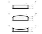
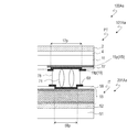
- FIG. 5A to 5C are schematic cross-sectional views of the liquid crystal panel 100a.
- FIG. 5A shows a state (room temperature (for example, 25° C.)) immediately after the liquid crystal layer LC is formed
- FIG. 5B shows a state after the liquid crystal layer LC is formed (for example, the temperature rises).
- 5C shows a state where the volume of the liquid crystal material has increased
- FIG. 5C shows a state where the volume of the liquid crystal material has decreased from the state of FIG. 5A (for example, due to the temperature drop).
- the dielectric material included in the TFT substrate 101a changes, as shown in FIGS. 5B and 5C, the dielectric material included in the TFT substrate 101a.
- the thickness of the liquid crystal layer LC changes due to the bending of the dielectric substrate 51 included in the substrate 1 and/or the slot substrate 201a.
- the dielectric substrates 1 and 51 are, for example, glass substrates.
- the thickness of the liquid crystal layer LC increases, and when the liquid crystal material contracts, the thickness of the liquid crystal layer LC decreases.
- 5B and 5C show only the flexure of the slot substrate 201a for the sake of clarity, the flexure of the TFT substrate 101a is not excluded.
- the seal portion 73a includes, for example, a granular spacer that controls the cell gap, the change in the distance between the TFT substrate 101a and the slot substrate 201a in the seal portion 73a is caused by the bending of the TFT substrate 101a and/or the slot substrate 201a. It is considered small compared to.
- a columnar spacer for controlling the cell gap is provided in the transmission/reception region R1. That is, in order to make the thickness of the liquid crystal layer LC uniform, at least one of the TFT substrate 101a and the slot substrate 201a is provided with a columnar photo spacer formed of an ultraviolet curable resin. Therefore, even if the temperature drops and the liquid crystal material thermally contracts, the columnar spacer suppresses the change in the cell gap, so that the TFT substrate 101a and/or the slot substrate 201a does not bend as shown in FIG. 5C. It is suppressed to some extent.
- vacuum bubbles may occur around the columnar spacer at low temperatures.
- the vacuum bubbles thus generated are sometimes called "low temperature bubbles”.
- Vacuum bubbles may be generated around the columnar spacers in the transmission/reception region R1 to change the capacitance value of the liquid crystal capacitance, and as a result, the antenna characteristics may deteriorate.
- the scanning antenna according to the embodiment of the present invention can suppress deterioration of the antenna performance from high temperature to low temperature.
- FIG. 6 is a schematic plan view of one liquid crystal panel 100Aa when the liquid crystal panel of the scanning antenna according to the first embodiment of the present invention is manufactured by tiling four liquid crystal panels.
- 7A to 7C are schematic cross-sectional views of the liquid crystal panel 100Aa.
- FIG. 7A shows a state (room temperature (for example, 25° C.)) immediately after the liquid crystal layer LC is formed
- FIG. 7B shows a state (for example, temperature rises) from the state of FIG. 7A
- 7C shows a state in which the volume of the liquid crystal material has increased
- FIG. 7C shows a state in which the volume of the liquid crystal material has decreased from the state of FIG. 7A (for example, due to the temperature drop).
- the same components as those of the scanning antenna 1000 are designated by the same reference numerals and the description thereof may be omitted.
- the scanning antenna is divided into four and manufactured, but it goes without saying that the embodiment of the present invention is not limited to this.
- liquid crystal layer LC refers to a region between the TFT substrate 101Aa and the slot substrate 201Aa and surrounded by the seal portion 73Aa. As a result, it is possible to suppress an increase in the thickness of the liquid crystal layer at a high temperature, so that it is possible to suppress deterioration of the antenna performance.
- vacuum bubbles (vacuum region) BB can be formed in the liquid crystal layer LC by adjusting the supply amount of the liquid crystal material.
- the vacuum bubble BB absorbs the volume change of the liquid crystal material, so that the liquid crystal layer LC.
- the change of the thickness is suppressed. That is, the deflection of the dielectric substrate (eg, glass substrate) of the TFT substrate 101Aa and/or the slot substrate 201Aa is suppressed.
- the volume of the vacuum bubble BB decreases, and when the liquid crystal material contracts, the volume of the vacuum bubble BB increases.
- the deformation (deflection) of the TFT substrate 101Aa and the slot substrate 201Aa can be avoided. It is considered that the thickness of the liquid crystal layer LC does not change as long as the vacuum bubble BB remains.
- the liquid crystal panel 100Aa having the structure shown in FIG. 6 can also obtain the following effects.
- the liquid crystal material thermally contracts, it is possible to suppress the generation of vacuum bubbles (low temperature bubbles) around the columnar spacers in the transmission/reception region R1. Further, the position of the vacuum bubble (vacuum region) generated in the step of forming the liquid crystal layer LC can also be controlled. Thereby, the deterioration of the antenna performance due to the vacuum bubbles can be suppressed.
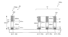
- the seal portion 73Aa of the liquid crystal panel 100Aa includes a wide gap portion 77 in which the gap between the first dielectric substrate 1 and the second dielectric substrate 51 is partially wide in the non-transmission/reception region R2. That is, in the gap between the first dielectric substrate 1 and the second dielectric substrate 51 in the wide gap portion 77, the first dielectric substrate 1 and the second dielectric substrate 51 in the portion other than the wide gap portion 77 of the seal portion 73Aa. Larger than the gap between. The gap between the first dielectric substrate 1 and the second dielectric substrate 51 in the wide gap portion 77 is larger than the gap between the first dielectric substrate 1 and the second dielectric substrate 51 in the transmission/reception region R1.
- a portion of the seal portion 73Aa other than the wide gap portion 77 includes a first granular spacer that defines the thickness of the liquid crystal layer LC in the transmission/reception region R1, and the wide gap portion 77 has a grain size smaller than that of the first granular spacer. Includes a large second granular spacer.
- the wide gap portion 77 is a portion of the seal portion 73Aa indicated by a thick line.
- the seal portion Rs1 provided in the transmission/reception region R1 of the seal portion 73Aa is shown by a dotted line.
- the wide gap part 77 is provided in the seal part Rs2 provided in the non-transmission/reception region R2. As shown in FIG.
- the liquid crystal panel 100Aa is a quarter panel in which one scanning antenna is formed by tiling.
- the boundary line between the transmission/reception region R1 and the non-transmission/reception region R2 can be, for example, a line including a point separated by 2 mm or more from the outermost antenna unit.
- the entire seal portion may also serve as the wide gap portion.
- the gap between the first dielectric substrate 1 and the second dielectric substrate 51 in the wide gap portion 77 is smaller than the gap between the first dielectric substrate 1 and the second dielectric substrate 51 in the transmission/reception region R1.
- low-temperature bubbles can be preferentially generated around the wide gap portion 77, and vacuum bubbles can be suppressed from being generated around the columnar spacers in the transmission/reception region R1. This suppresses the deterioration of the antenna performance.
- the seal part Rs2 provided in the non-transmission/reception region R2 includes a point separated from the transmission/reception region R1 by 2 mm or more.
- the position of the wide gap part 77 in the seal part 73Aa By selecting the position of the wide gap part 77 in the seal part 73Aa, the position of the vacuum bubble (vacuum region) generated in the process of forming the liquid crystal layer LC can also be controlled. This is because in the process of forming the liquid crystal layer LC, vacuum bubbles (vacuum regions) tend to be easily formed along the wide gap portion 77. As a result, it is possible to suppress deterioration of the antenna performance even at room temperature, for example.
- the scanning antenna having the liquid crystal panel 100Aa it is possible to suppress deterioration of the antenna performance from a high temperature to a low temperature (including a case where the liquid crystal material is thermally expanded and a case where the liquid crystal material is thermally contracted).
- the following scanning antenna is not limited to the exemplified one, and can obtain this effect; (1) In the step of forming the liquid crystal layer, the liquid crystal layer (that is, between the TFT substrate and the slot substrate) is formed.
- a vacuum bubble (vacuum region) is generated in a region surrounded by the seal portion, and (2) a gap between the first dielectric substrate 1 and the second dielectric substrate 51 in the transmission/reception region R1 ( A spacer structure that defines a gap between the first dielectric substrate 1 and the second dielectric substrate 51 that is larger than the “first gap”) is provided in the seal portion or in the seal portion of the non-transmission/reception region R2. It only needs to be in the enclosed area.
- the “spacer structure” includes all conductive layers, insulating layers, and spacers (columnar spacers, granular spacers, etc.) included between the first dielectric substrate 1 and the second dielectric substrate 51. Including.
- the spacer arranged in the transmission/reception region R1 and defining the first gap may be referred to as a first spacer structure.
- the first spacer structure includes a columnar spacer.
- the first spacer structure typically includes a columnar spacer that defines the thickness of the liquid crystal layer LC between the patch electrode 15 and the slot electrode 55.
- the scanning antenna according to the embodiment of the present invention may have the second spacer structure higher than the first spacer structure in the non-transmission/reception region R2 of the region surrounded by the seal portion.
- the height of the first spacer structure that defines the first gap is 1, the height of the second spacer structure is preferably 1.1 or more and 2.0 or less, for example.
- the difference between the height of the first spacer structure and the height of the second spacer structure is, for example, 0.9 ⁇ m or more and 3 ⁇ m or less. If the height of the second spacer structure is higher than that of the first spacer structure, the thickness of the liquid crystal layer LC in the transmission/reception region R1 may be affected.
- the method of making the second spacer structure higher than the first spacer structure may be arbitrary.
- the particle size of the granular spacer or the height of the columnar spacer may be changed.
- the second spacer structure may include a spacer higher than the columnar spacer (for example, the columnar spacer that defines the thickness of the liquid crystal layer LC between the patch electrode 15 and the slot electrode 55) included in the first spacer structure.
- the laminated structure of the conductive layer and the insulating layer included in the TFT substrate and the slot substrate may be different between the first spacer structure and the second spacer structure.
- the first spacer structure may not include the conductive layer and the second spacer structure may include the conductive layer by patterning the conductive layer.
- the first spacer structure may not include the insulating layer and the second spacer structure may include the opening by forming an opening in the insulating layer.
- either the conductive layer or the insulating layer included in the TFT substrate and the slot substrate may have different thicknesses between the first spacer structure and the second spacer structure.
- a combination of any of the above may be used.
- the liquid crystal layer may be formed by a vacuum injection method or a drop injection method.
- the vacuum injection method for example, the supply of the liquid crystal material may be stopped in the state where the vacuum region exists between the TFT substrate and the slot substrate and in the region surrounded by the seal portion.
- the drop injection method for example, the liquid crystal material may be dropped in an amount smaller than the volume required to fill the entire area surrounded by the seal portion.
- vacuum bubbles in the liquid crystal layer LC in the non-transmission/reception region R2.
- vacuum bubbles in the process of forming the liquid crystal layer LC, vacuum bubbles (vacuum regions) tend to be easily formed along the wide gap portion 77, so the wide gap portion 77 is arranged at a position far from the transmission/reception region R1.
- the temperature of the liquid crystal layer is increased to, for example, 120° C. or higher (or the Tni point or higher, for example), and then the temperature is lowered to control the position of the vacuum bubble (vacuum region) formed in the liquid crystal layer. May be.
- the position of the vacuum bubble can be controlled with higher accuracy. That is, when the liquid crystal layer is heated, as described above, the volume of the liquid crystal material increases, so that the volume of the vacuum bubble (vacuum region) decreases. For example, when the temperature of the liquid crystal layer is raised to such an extent that the vacuum bubble (vacuum region) disappears, and then the temperature is lowered, as described above, the vacuum bubble starts to be generated around the spacer that defines the largest cell gap. That is, the vacuum bubbles are mainly formed around the wide gap portion 77. In addition, by providing an additional seal portion to be described later, it is possible to perform control with higher accuracy so that vacuum bubbles (vacuum region) are easily generated in the liquid crystal layer of the non-transmission/reception region R2. When the drop injection method is used, the liquid crystal material may be preferentially dropped in the transmission/reception region R1.
- a region to be a display region is filled with a liquid crystal material without excess or deficiency, and a partition is formed inside the seal portion in order to suppress generation of vacuum bubbles and variation in thickness of the liquid crystal layer in the display region.
- the partition is formed of a sealing material and has a slit. The partition divides the display area and the buffer area, and the liquid crystal material in the display area can flow to the buffer area through the slit.
- the gap between the substrates in the buffer region is larger than the gap between the substrates in the display region.
- a first granular spacer that defines the thickness of the liquid crystal layer LC in the transmission/reception region R1 is arranged in a portion other than the wide gap portion 77 in the seal portion 73Aa, and the wide gap portion 77 has a size greater than that of the first granular spacer.
- a second granular spacer having a large particle size may be arranged.
- the spacer structure included in the wide gap portion 77 (which may be referred to as a second spacer structure) includes the second granular spacer.
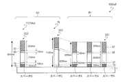
- FIGS. 8A to 8D schematically show plan views of liquid crystal panels 100Aa1 to 100Aa4 which are modified examples of the liquid crystal panel 100Aa.
- the liquid crystal panels 100Aa1 to 100Aa4 respectively have additional seal portions 76A to 76D (generally referred to as “additional seal portions 76”) instead of the wide gap portion 77.
- the additional seal portion 76 defines a gap between the first dielectric substrate 1 and the second dielectric substrate 51 that is wider than the first gap.
- the liquid crystal panels 100Aa1 to 100Aa4 have the additional seal part 76 in the non-transmission/reception region R2 in the region surrounded by the seal part 73Aa, so that in the process of forming the liquid crystal layer, a vacuum bubble (vacuum region) is generated.
- the position can be controlled with higher accuracy.
- the area surrounded by the seal portion 73Aa is divided into the active area Ra including the transmission/reception area R1 and the buffer area Rb other than the active area Ra by the additional seal portion 76.
- the active region Ra and the buffer region Rb are not completely blocked, and the liquid crystal material can move between the active region Ra and the buffer region Rb.
- the additional seal portion 76 is preferably far from the transmission/reception region R1. This is because, for the same reason as the wide gap portion 77 described above, low temperature bubbles are likely to be generated around the additional seal portion 76.
- the additional seal portions 76A and 76B are configured so that the liquid crystal material injected from the injection port 74a is filled in the buffer region Rb through the active region Ra. Has been formed.
- the width Wb of the entrance of the buffer region Rb as in the additional seal portion 76B shown in FIG. 8B it is possible to reduce the speed at which the liquid crystal material is filled in the buffer region Rb. This makes it easy to control the volume of vacuum bubbles (vacuum region) in the liquid crystal layer LC.
- the buffer region Rb is formed such that a region having a small width Wb continues for a long time.
- the width Wb is, for example, about 5 mm to 15 mm, for example, about 10 mm.
- the length of the region where the width Wb is substantially constant may be, for example, about 5 mm to 50 mm.
- the resin structure can be formed by a photolithography process using, for example, an ultraviolet curable resin.
- the resin structure can be formed, for example, by the same process as the columnar spacer provided in the transmission/reception region.
- the bottom area of the resin structure may be about the same as that of the columnar spacer, for example.
- the additional seal portion 76C may be formed so that the liquid crystal material is filled into the buffer region Rb from two inlets.
- the widths Wb1 and Wb2 of the two entrances may be the same or different, but are independently about 5 mm to 15 mm, for example.
- two buffer regions Rb1 and Rb2 may be formed by the two additional seal portions 76D1 and 76D2.
- the width of the entrance of each buffer area and the length of the area in which the width is substantially constant may be independently within the above-described preferable range.
- the additional seal part 76 has a larger granular particle size than the first granular spacer (for example, a particle size). 3.5 ⁇ m to 10 ⁇ m, including, for example, a particle size of 4 ⁇ m).
- the spacer structure included in the additional seal portion 76 includes granular spacers.
- the spacer structure included in the additional seal portion 76 may include columnar spacers instead of the granular spacers.
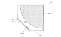
- the position where the additional seal portion 76 is formed is preferably the region Rg shown in FIG. 9A in the non-transmission/reception region R2 in the region surrounded by the seal portion 73Aa.
- the dielectric substrate 1 of the TFT substrate 101Aa and the dielectric substrate 51 of the slot substrate 201Aa are typically glass substrates. By cutting a rectangular (including square and rectangular) mother glass substrate into a desired shape, It is formed. An example of the shape of the mother glass substrate is shown by a dashed line in FIG. As can be seen from FIG. 9A, even if the region Rg is widened, the influence on the size of the mother glass substrate and the size of the transmission/reception region included in the liquid crystal panel manufactured from the mother glass substrate is small.
- the additional seal portion 76 is formed in a region along the side where the cutout from the rectangle is the largest when the smallest rectangle including the liquid crystal panel is drawn when viewed from the normal direction of the dielectric substrate 1. It is preferable to include a portion.
- the additional seal portion 76 defines a distance to the edge of the liquid crystal panel 100Aa in the normal direction of each point on the edge of the transmission/reception region R1 when viewed from the normal direction of the dielectric substrate 1, the distance is the largest. It is preferably formed in a region including a large portion.
- a plurality of TFT substrates or slot substrates may be formed from one mother glass substrate.
- the shape and position of the additional seal part are not limited to those shown in the figure.
- the shape and position of the additional seal portion and the volume of the vacuum bubble (vacuum region) generated in the process of forming the liquid crystal layer LC can be appropriately adjusted depending on the characteristics of the liquid crystal material, the ambient temperature of the scanning antenna, and the like. preferable. If the volume of the vacuum bubble (vacuum region) generated in the step of forming the liquid crystal layer LC is large, the effect of suppressing the change in the thickness of the liquid crystal layer due to the change in volume of the liquid crystal material (especially at the time of thermal expansion) is increased, On the other hand, the possibility that vacuum bubbles (vacuum region) will be generated in the transmission/reception region R1 also increases.
- the vacuum region generated in the step of forming the liquid crystal layer LC is, for example, about 5% to 20% of the area within the region surrounded by the seal portion 73Aa when viewed from the normal direction of the dielectric substrate 1 or 51. Is.
- the volume of vacuum bubbles (vacuum region) generated in the step of forming the liquid crystal layer LC may be adjusted so that the vacuum region disappears when the temperature becomes high (for example, 120° C. or higher). This temperature takes into consideration, for example, the environmental temperature (for example, 20° C. to 70° C.) where the scanning antenna may be installed, the Tni point of the liquid crystal material, the temperature reached by the liquid crystal material in the manufacturing process (for example, heat treatment), and the like. And decide.
- the volume of the vacuum bubble (vacuum region) to be formed becomes larger when the spacer structure included in the additional seal portion 76 is made higher (for example, when the particle size of the granular spacer included in the spacer structure included in the additional seal portion 76 is increased). Be done.
- the difference between the height of the spacer structure included in the additional seal portion 76 and the height of the spacer structure provided in the transmission/reception region R1 is, for example, 500 nm to 5000 nm.
- the additional seal part is not limited to one that divides the area surrounded by the seal part into an active area and a buffer area other than the active area.
- a plurality of the above resin structures may be arranged.
- the additional seal portion When viewed in the normal direction of the dielectric substrate 1 or 51, the additional seal portion may have a dot shape.
- the liquid crystal panel according to the embodiment of the present invention has the above-mentioned addition in addition to the wide gap portion. You may have the sealing part 76.
- FIG. 9B schematically shows another modified liquid crystal panel 100Aa5.
- the liquid crystal panel 100Aa5 has a wide gap portion 77 and an additional seal portion 76B.
- the wide gap portion 77 defines a gap between the first dielectric substrate 1 and the second dielectric substrate 51, which is wider than the first gap, so that the wide gap portion 77 and the first dielectric substrate 1 defined by the additional seal portion 76B.
- the gap with the second dielectric substrate 51 may be the same as the first gap or may be larger than the first gap.
- the gap between the first dielectric substrate 1 and the second dielectric substrate 51 defined by the additional seal portion 76B is the gap between the first dielectric substrate 1 and the second dielectric substrate 51 defined by the wide gap portion 77. It may be larger or smaller than.
- FIG. 10A to 10E are schematic cross-sectional views for explaining the method for manufacturing the TFT substrate 101Aa
- FIG. 10F is a schematic cross-sectional view showing the TFT substrate 101Aa.
- the structure and manufacturing method of the TFT substrate included in the scanning antenna according to the embodiment of the present invention are not limited to the exemplified ones.
- the TFT substrate 101Aa shown in FIG. 10(f) has a dielectric substrate 1 and a plurality of antenna unit regions U arranged on the dielectric substrate 1.
- Each of the plurality of antenna unit regions U has a TFT 10A and a patch electrode 15 electrically connected to the drain electrode 7D of the TFT 10A.
- the TFT substrate 101Aa includes a gate metal layer 3 supported by the dielectric substrate 1, a gate insulating layer 4 formed on the gate metal layer 3, and a gate insulating layer 4 on the gate insulating layer 4.
- the source metal layer 7 formed, the first insulating layer 11 formed on the source metal layer 7, the patch metal layer 15l formed on the first insulating layer 11, and the patch metal layer 15l formed And a second insulating layer 17.
- the source metal layer 7 has a lower layer S1 and an upper layer S2 formed on the lower layer S1.
- the TFT substrate 101Aa further has an upper conductive layer 19 formed on the second insulating layer 17, as shown in the structure of the non-transmission/reception region R2 (transfer portion) in FIG. 12 described later.
- the TFT 10A included in each antenna unit region U includes a gate electrode 3G, an island-shaped semiconductor layer 5, contact layers 6S and 6D, a gate insulating layer 4 arranged between the gate electrode 3G and the semiconductor layer 5, A source electrode 7S and a drain electrode 7D are provided.
- the TFT 10A is a channel-etch type TFT having a bottom gate structure.
- the gate electrode 3G is electrically connected to the gate bus line, and a scanning signal is supplied from the gate bus line.
- the source electrode 7S is electrically connected to the source bus line and is supplied with a data signal from the source bus line.
- the gate electrode 3G and the gate bus line may be formed of the same conductive film (conductive film for gate).
- the source electrode 7S, the drain electrode 7D, and the source bus line may be formed of the same conductive film (source conductive film).
- the gate conductive film and the source conductive film are, for example, metal films.
- a layer formed using a conductive film for gate is sometimes referred to as a “gate metal layer”, and a layer formed using a conductive film for source is referred to as a “source metal layer”.
- the layer including the patch electrode 15 formed of the patch conductive film may be referred to as a “patch metal layer”.
- the semiconductor layer 5 is arranged so as to overlap the gate electrode 3G via the gate insulating layer 4.
- the source contact layer 6S and the drain contact layer 6D are formed on the semiconductor layer 5.
- the source contact layer 6S and the drain contact layer 6D are respectively arranged on both sides of a region (channel region) where a channel is formed in the semiconductor layer 5.
- the semiconductor layer 5 is an intrinsic amorphous silicon (ia-Si) layer
- the source contact layer 6S and the drain contact layer 6D are n + type amorphous silicon (n + -a-Si) layers.
- the source electrode 7S is provided in contact with the source contact layer 6S, and is connected to the semiconductor layer 5 via the source contact layer 6S.
- the drain electrode 7D is provided so as to be in contact with the drain contact layer 6D, and is connected to the semiconductor layer 5 via the drain contact layer 6D.
- the first insulating layer 11 has an opening 11a reaching the drain electrode 7D of the TFT 10A.
- the patch electrode 15 is provided on the first insulating layer 11 and in the opening 11a, and is in contact with the drain electrode 7D in the opening 11a.
- the patch electrode 15 includes a metal layer.
- the patch electrode 15 may be a metal electrode formed of only a metal layer.
- the patch electrode 15 may include a Cu layer or an Al layer as a main layer.
- the performance of the scanning antenna has a correlation with the electric resistance of the patch electrode 15, and the thickness of the main layer is set so as to obtain a desired resistance. From the viewpoint of electrical resistance, the Cu layer may be able to make the thickness of the patch electrode 15 smaller than that of the Al layer.
- Each antenna unit area U may have an auxiliary capacitance electrically connected in parallel with the liquid crystal capacitance.
- the auxiliary capacitance is composed of, for example, an upper auxiliary capacitance electrode electrically connected to the drain electrode 7D, a gate insulating layer 4, and a lower auxiliary capacitance electrode facing the upper auxiliary capacitance electrode via the gate insulating layer 4.
- the lower auxiliary capacitance electrode is included in the gate metal layer 3
- the upper auxiliary capacitance electrode is included in the source metal layer 7.
- the gate metal layer 3 may further include a CS bus line (auxiliary capacitance line) connected to the lower auxiliary capacitance electrode.
- FIG. 12 is a cross-sectional view schematically showing a structure of a transfer part included in the TFT substrate 101Aa and the slot substrate 201Aa.
- the structure of the transfer terminal portion PT of the TFT substrate 101Aa will be described with reference to FIG.
- the transfer terminal portion PT includes a patch connecting portion 15p formed on the first insulating layer 11, a second insulating layer 17 covering the patch connecting portion 15p, and a transfer terminal upper connecting portion 19p. have.
- the transfer terminal upper connecting portion 19p is in contact with the patch connecting portion 15p in the opening 17p formed in the second insulating layer 17.
- the patch connection portion 15p is included in the patch metal layer 151.
- the transfer terminal upper connection portion 19p (may be simply referred to as “upper connection portion 19p”) is included in the upper conductive layer 19 formed on the second insulating layer 17 here.
- a method of manufacturing the TFT substrate 101Aa will be described with reference to FIGS. 10(a) to 10(e).
- the gate metal layer 3 including the gate electrode 3G is formed on the dielectric substrate 1.
- the gate electrode 3G can be formed integrally with the gate bus line.
- a gate conductive film (not shown) is formed on the dielectric substrate 1 by a sputtering method or the like.
- the gate conductive film is patterned to obtain the gate electrode 3G.
- the material of the conductive film for gate is not particularly limited.
- a film containing a metal such as aluminum (Al), tungsten (W), molybdenum (Mo), tantalum (Ta), chromium (Cr), titanium (Ti), copper (Cu), or an alloy thereof, or a metal nitride thereof is used. It can be used as appropriate.
- a Cu film (thickness: for example, 200 nm to 500 nm) is used as the gate conductive film.
- a laminated film (Cu/Ti) in which a Ti film (thickness: 20 nm to 100 nm) and a Cu film (thickness: 200 nm to 500 nm) are laminated in this order may be used as the conductive film for gate.
- the Ti film thickness: 20 nm to 100 nm
- a Cu film thickness: 200 nm to 500 nm
- the patterning of the gate conductive film is performed by photolithography, wet etching, and resist peeling cleaning.
- the gate insulating layer 4, the semiconductor layer 5, and the contact layer 6a are formed.
- the gate insulating layer 4 can be formed by a CVD method or the like.
- the gate insulating layer 4 includes a silicon oxide (SiO x ) layer, a silicon nitride (SiN x ) layer, a silicon oxynitride (SiO x N y (x>y)) layer, and a silicon nitride oxide (SiN x O y (x>). y)) layer etc. can be used suitably.
- the gate insulating layer 4 may have a laminated structure.
- a SiN x layer (thickness: 100 nm to 500 nm, for example) is formed as the gate insulating layer 4.
- the semiconductor layer 5 and the contact layer 6a are formed on the gate insulating layer 4.
- an intrinsic amorphous silicon film thickness: eg 30 nm to 300 nm
- an n + type amorphous silicon film thickness: eg 50 nm to 150 nm
- photolithography, dry etching and resist peeling cleaning are performed.
- the island-shaped semiconductor layer 5 and the contact layer 6a are obtained by patterning.
- a conductive film for a source is formed on the gate insulating layer 4 and the contact layer 6a and patterned to form a source metal including a source electrode 7S and a drain electrode 7D as shown in FIG. 10C.
- a source metal including a source electrode 7S and a drain electrode 7D as shown in FIG. 10C.
- the contact layer 6a is also etched to form the source contact layer 6S and the drain contact layer 6D which are separated from each other.
- the material of the conductive film for source is not particularly limited.
- a film containing a metal such as aluminum (Al), tungsten (W), molybdenum (Mo), tantalum (Ta), chromium (Cr), titanium (Ti), copper (Cu), or an alloy thereof, or a metal nitride thereof is used. It can be used as appropriate.
- a laminated film (Cu/Ti) is formed by laminating a Ti film (thickness: 20 nm to 100 nm) and a Cu film (thickness: 100 nm to 400 nm) in this order.
- a conductive film for a source (Ti film and Cu film) is formed by a sputtering method, and this is subjected to photolithography, etching (after the Cu film is wet-etched, the Ti film and the contact layer 6a are dry-etched), and By performing the resist peeling cleaning in this order, the source metal layer 7 having the lower layer S1 and the upper layer S2 is obtained.
- the dry etching step the portion of the contact layer 6a located on the region to be the channel region of the semiconductor layer 5 is removed to form a gap portion, and the source contact layer 6S and the drain contact layer 6D are obtained.
- the vicinity of the surface of the semiconductor layer 5 can also be etched in the gap portion (overetching). In this way, the TFT 10A is obtained.
- a first insulating layer 11 is formed so as to cover the TFT 10A, and an opening reaching the drain electrode 7D is formed in the first insulating layer 11 by known photolithography and dry etching. 11a is formed.
- the first insulating layer 11 is arranged so as to be in contact with the channel region of the semiconductor layer 5.
- the first insulating layer 11 is, for example, a silicon oxide (SiO x ) film, a silicon nitride (SiN x ) film, a silicon oxynitride (SiO x N y (x>y)) film, and a silicon nitride oxide (SiN x O y (SiN x O y ( It may be an inorganic insulating layer such as x>y)) film.
- a SiN x film thickness: for example, 100 nm to 500 nm
- the CVD method is formed by, for example, the CVD method.
- the opening may be formed in the gate insulating layer 4 in this step.
- the lower connecting portion of the terminal portion provided in the non-transmission/reception region R2 is formed of the gate metal layer 3
- the opening reaching the lower connecting portion is formed in the gate insulating layer 4 and the first insulating layer 11.
- the gate insulating layer 4 and the first insulating layer 11 may be collectively etched by dry etching using a fluorine-based gas.
- a patch conductive film is formed on the first insulating layer 11 and in the opening 11a, and this is patterned to form a patch electrode 15 as shown in FIG. 10(e).
- the patch connection portion 15p is formed in the transfer terminal portion formation region of the non-transmission/reception region R2.
- the patch electrode 15 contacts the drain electrode 7D in the opening 11a.
- the same material as the conductive film for gate or the conductive film for source may be used.
- the patch conductive film may be set to be thicker than the gate conductive film and the source conductive film. As a result, by reducing the sheet resistance of the patch electrode, it is possible to reduce the loss in which the vibration of free electrons in the patch electrode is converted into heat.
- a Cu film (thickness: for example, 200 nm to 1000 nm) is used as the patch conductive film.
- a laminated film (Cu/Ti) in which a Ti film (thickness: 20 nm to 100 nm) and a Cu film (thickness: 200 nm to 1000 nm) are laminated in this order may be used.
- the patterning of the patch conductive film is performed by photolithography, wet etching, and resist peeling cleaning.
- the second insulating layer 17 is formed on the patch electrode 15 and the first insulating layer 11. After that, an opening 17p reaching the patch connection portion 15p is formed in the second insulating layer 17 by known photolithography and dry etching.
- the second insulating layer 17 is not particularly limited and includes, for example, a silicon oxide (SiO x ) film, a silicon nitride (SiN x ) film, a silicon oxynitride (SiO x N y (x>y)) film, and a silicon nitride oxide ( A SiN x O y (x>y)) film or the like can be used as appropriate.
- a SiN x layer thickness: for example, 50 nm to 400 nm
- a transparent conductive film (thickness: for example, 50 nm or more and 150 nm or less) is formed on the second insulating layer 17 and in the opening formed in the second insulating layer 17 by, for example, a sputtering method.
- the transparent conductive film for example, an ITO (indium tin oxide) film, an IZO film, a ZnO film (zinc oxide film) or the like can be used.
- the transparent conductive film may have a laminated structure including a Ti film (thickness: for example, 20 nm or more and 50 nm or less) and an ITO film, an IZO film, or a ZnO film in this order.
- the transparent conductive film includes the Ti film, in the transfer terminal portion PT, the corrosion of the patch connecting portion 15p is suppressed and/or the contact resistance between the patch connecting portion 15p and the upper connecting portion 19p is reduced.
- the transparent conductive film is patterned by photolithography, wet etching, and resist peeling cleaning to obtain the upper conductive layer 19 including the transfer terminal upper connecting portion 19p.
- an annealing process may be further performed. By applying an annealing treatment to the transparent conductive film, it is possible to reduce the resistance.
- the TFT substrate 101Aa is obtained.
- the antenna unit area of the TFT substrate 101Aa is illustrated and described, but the terminal portion provided in the non-transmission/reception area R2, the TFT included in the drive circuit (gate driver, source driver, etc.), etc. are also subjected to the above steps. It may be formed at the same time as the antenna unit area.
- FIG. 11A and 11B are schematic cross-sectional views for explaining the method for manufacturing the slot substrate 201Aa, and FIG. 11C shows the antenna unit area U and the seal portion 73Aa in the slot substrate 201Aa. It is sectional drawing which shows typically.
- FIG. 11D is a sectional view schematically showing the antenna unit area U and the seal portion 73Aa in the liquid crystal panel 100Aa.
- the slot substrate 201Aa includes a dielectric substrate 51 having a front surface and a back surface, a third insulating layer 52 formed on the front surface of the dielectric substrate 51, and a third insulating layer.
- a slot electrode 55 formed on the layer 52 and a fourth insulating layer 58 covering the slot electrode 55 are provided.
- the reflective conductive plate 65 (see FIG. 1) is arranged so as to face the back surface of the dielectric substrate 51 via the dielectric layer (air layer) 54.
- the slot electrode 55 and the reflective conductive plate 65 function as a wall of the waveguide 301.
- a plurality of slots 57 are formed in the slot electrode 55 in the transmission/reception region R1.
- the slot 57 is an opening that penetrates the slot electrode 55.
- one slot 57 is arranged in each antenna unit area U.
- the fourth insulating layer 58 is formed on the slot electrode 55 and inside the slot 57.
- the fourth insulating layer 58 has, for example, an opening 58a that reaches the third insulating layer 52 in the slot 57.
- the material of the fourth insulating layer 58 may be the same as the material of the third insulating layer 52.
- the fourth insulating layer 58 can prevent the liquid crystal material from entering the voids in the Al layer.
- the problem of voids can be avoided by forming an Al layer by adhering an aluminum foil to the dielectric substrate 51 with an adhesive and then patterning this to form the slot electrode 55.
- the slot electrode 55 includes main layers such as a Cu layer and an Al layer.
- the slot electrode 55 may have a laminated structure including a main layer and an upper layer and/or a lower layer arranged so as to sandwich the main layer.
- the thickness of the main layer is set in consideration of the skin effect depending on the material, and may be, for example, 2 ⁇ m or more and 30 ⁇ m or less.
- the thickness of the main layer is typically greater than the thickness of the upper and lower layers.
- the main layer is a Cu layer and the upper and lower layers are Ti layers.
- the reflective conductive plate 65 constitutes the wall of the waveguide 301, it preferably has a thickness of 3 times or more, preferably 5 times or more of the skin depth.
- the reflective conductive plate 65 for example, an aluminum plate or a copper plate having a thickness of several mm, which is manufactured by shaving, can be used.
- the terminal portion IT is provided in the non-transmission/reception area R2 of the slot board 201Aa.
- the terminal portion IT includes a slot electrode 55, a fourth insulating layer 58 that covers the slot electrode 55, and an upper connection portion 60.
- the fourth insulating layer 58 has an opening 58p reaching the slot electrode 55.
- the upper connection portion 60 is in contact with the slot electrode 55 within the opening 58p.
- the upper connection portion 60 of the terminal portion IT of the slot substrate 201Aa is electrically connected to the transfer terminal upper connection portion 19p of the transfer terminal portion PT of the TFT substrate 101Aa.
- the upper connecting portion 60 and the transfer terminal upper connecting portion 19p are connected via a resin (for example, a sealing resin) 78 containing the conductive beads 71.
- the upper connection parts 60 and 19p are both transparent conductive layers such as an ITO film and an IZO film, and an oxide film may be formed on the surface thereof.
- an oxide film may be formed on the surface thereof.
- the oxide film is formed, electrical connection between the transparent conductive layers cannot be secured, and the contact resistance may increase.
- the conductive beads for example, Au beads
- the conductive beads are not By breaking through (penetrating) the oxide film, it is possible to suppress an increase in contact resistance.
- the conductive beads 71 may penetrate not only the surface oxide film but also the upper connecting portions 60 and 19p, which are transparent conductive layers, and may be in direct contact with the patch connecting portion 15p and the slot electrode 55.
- seal region Rs may also have the same structure as the transfer portion described above. That is, the transfer part may be arranged in the seal region Rs (seal part 73Aa).
- the slot board 201Aa can be manufactured, for example, by the following method.
- the third insulating layer 52 (thickness: for example, 300 nm to 1500 nm) is formed on the dielectric substrate 51 by, for example, the CVD method.
- a substrate having a high transmittance for electromagnetic waves small permittivity ⁇ M and dielectric loss tan ⁇ M
- the dielectric substrate 51 is preferably thin in order to suppress attenuation of electromagnetic waves.
- the glass substrate may be thinned from the rear surface side after the constituent elements such as the slot electrodes 55 are formed on the front surface of the glass substrate by a process described later. Thereby, the thickness of the glass substrate can be reduced to, for example, 500 ⁇ m or less.
- constituent elements such as TFTs may be directly formed on the resin substrate, or may be formed on the resin substrate by using a transfer method.
- the transfer method for example, after forming a resin film (for example, a polyimide film) on a glass substrate and forming components on the resin film by a process described below, the resin film on which the components are formed and the glass substrate are separated from each other. Separate.
- resin has a smaller dielectric constant ⁇ M and dielectric loss tan ⁇ M than glass.
- the thickness of the resin substrate is, for example, 3 ⁇ m to 300 ⁇ m.
- the resin material other than polyimide, for example, liquid crystal polymer can be used.
- the third insulating layer 52 is not particularly limited, but for example, a silicon oxide (SiO x ) film, a silicon nitride (SiN x ) film, a silicon oxynitride (SiO x N y (x>y)) film, a silicon nitride oxide ( A SiN x O y (x>y)) film or the like can be used as appropriate.
- a metal film for example, a Cu film or an Al film
- a metal film is formed on the third insulating layer 52 by, for example, a sputtering method, and this is patterned to form a plurality of slots 57 as shown in FIG. 11A.
- the slot electrode 55 having is obtained.
- a Cu film having a thickness of 1000 nm to 4000 nm may be used as the metal film.
- a laminated film (Cu/Ti) in which Ti (thickness: eg, 20 nm to 100 nm) and Cu (thickness: eg, 1000 nm to 4000 nm) are laminated in this order may be formed.
- a fourth insulating layer 58 (thickness: 50 nm to 400 nm) is formed on the slot electrode 55 and inside the slot 57.
- the material of the fourth insulating layer 58 may be the same as the material of the third insulating layer.
- the opening 58p reaching the slot electrode 55 is formed in the fourth insulating layer 58 in the non-transmission/reception region R2.
- the opening 58p can be formed by photolithography, dry etching, and resist peeling cleaning.
- a transparent conductive film (thickness: 50 nm to 150 nm, for example) is formed on the fourth insulating layer 58 and in the opening 58p of the fourth insulating layer 58 by, for example, a sputtering method, and the transparent conductive film is patterned to form the opening.
- An upper connection portion 60 that contacts the slot electrode 55 is formed in 58p. Thereby, the terminal portion IT can be obtained.
- the transparent conductive film for example, an ITO (indium tin oxide) film, an IZO film, a ZnO film (zinc oxide film) or the like can be used.
- the transparent conductive film may have a laminated structure including a Ti film (thickness: 20 nm to 50 nm, for example) and an ITO film, an IZO film, or a ZnO film in this order.
- a Ti film thickness: 20 nm to 50 nm, for example
- an ITO film i.g., aluminum oxide
- an IZO film i.g., zinc antimonide
- a ZnO film in this order.
- a transparent conductive layer is obtained by patterning the transparent conductive film by photolithography, wet etching, and resist peeling cleaning. After patterning the transparent conductive film, an annealing treatment for reducing the resistance may be further performed.
- a photosensitive resin film is formed on the fourth insulating layer 58 and on the transparent conductive layer formed on the fourth insulating layer 58, and openings of a predetermined pattern are formed.
- the columnar spacers PS are formed by exposing and developing the photosensitive resin film through the photomask provided.
- the photosensitive resin may be a negative type or a positive type.
- the slot board 201Aa is manufactured.
- the TFT substrate has the columnar spacers PS
- a photosensitive resin film is formed on the second insulating layer 17 and the upper conductive layer 19, and the exposure and development are performed. By doing so, the columnar spacer may be formed.
- the liquid crystal panel 100Aa is manufactured by bonding the TFT substrate 101Aa and the slot substrate 201Aa manufactured as described above.
- the seal portion 73Aa is formed as follows. On one of the slot substrate 201Aa and the TFT substrate 101Aa (for example, the TFT substrate 101Aa), using a dispenser, for example, a pattern having an opening at a portion to be the injection port 74a is drawn with a sealing material. Further, a seal resin containing conductive particles is applied to the terminal portion of one substrate (the terminal portion PT of the TFT substrate 101Aa or the terminal portion IT of the slot substrate 201Aa). Instead of drawing the sealing material with the dispenser, for example, the sealing material may be applied in a predetermined pattern by screen printing.
- the sealing material is cured by stacking it on the other substrate and heating it at a predetermined pressure and a predetermined temperature for a predetermined time.
- Granular spacers for example, resin beads
- the gap in which the liquid crystal layer LC is formed is maintained between the slot substrate 201Aa and the TFT substrate 101Aa, and the spacers are mutually separated. Bonded and fixed. As a result, the main seal portion 75Aa is formed.
- the liquid crystal layer LC is formed.
- a liquid crystal material is injected from the injection port 74a by a vacuum injection method.
- a thermosetting encapsulant is applied so as to close the injection port 74a, and the encapsulant is cured by heating at a predetermined temperature for a predetermined time to form an end seal portion (not shown).
- the main seal portion 75Aa and the end seal portion thus form the entire seal portion 73Aa surrounding the liquid crystal layer LC.
- the liquid crystal layer LC may be formed by using the drop injection method.
- each liquid crystal panel may be cut out by, for example, dicing or laser processing. Good.
- FIG. 13 schematically shows an example of a spacer structure included in the liquid crystal panel 100Aa.
- a first spacer structure SS1 defining a gap (first gap) between the first dielectric substrate 1 and the second dielectric substrate 51 in the transmission/reception region R1, and a second spacer included in the wide gap portion 77.
- Structure SS2 is shown.
- the second spacer structure SS2 (height 6440 nm) is higher than the first spacer structure SS1 (height 6250 nm) (the difference in height between the first spacer structure SS1 and the second spacer structure SS2 is 0. 19 ⁇ m).
- examples of the heights of the conductive layer, the insulating layer and the spacer included in each spacer structure are shown.
- Spacer A in the figure indicates the height of the columnar spacers included in the first spacer structure SS1
- Spacer B is the height of the spacers (columnar spacers or granular spacers) included in the second spacer structure SS2. Is shown. However, illustration of the gate insulating layer 4, the first insulating layer 11, and the third insulating layer 52 is omitted.
- the first spacer structure SS1 and the second spacer structure SS2 both further include the gate insulating layer 4, the first insulating layer 11, and the third insulating layer 52, so that the gate insulating layer 4, the first insulating layer 52 The layer 11 and the third insulating layer 52 do not contribute to the difference in height between the first spacer structure SS1 and the second spacer structure SS2.
- FIG. 14 shows an example of the spacer structure included in the liquid crystal panel 100Aa5. As described above, the liquid crystal panel 100Aa5 further includes the additional seal portion 76.
- a first spacer structure SS1 that defines a gap (first gap) between the first dielectric substrate 1 and the second dielectric substrate 51 in the transmission/reception region R1, and a second spacer included in the wide gap portion 77.
- the structure SS2 and the third spacer structure SS3 included in the additional seal portion 76 are shown.
- the third spacer structure SS3 (height 7100 nm) is higher than the first spacer structure SS1 (height 6250 nm) (the difference in height between the first spacer structure SS1 and the third spacer structure SS3 is 0). .85 ⁇ m).
- Space C in the figure indicates the height of the spacer (columnar spacer or granular spacer) included in the third spacer structure SS3.
- the second spacer structure SS2 and the third spacer structure SS3 are higher than the first spacer structure SS1, and the third spacer structure SS3 is higher than the second spacer structure SS2 (the third spacer structure SS3 and the third spacer structure SS3).
- the height difference from the two-spacer structure SS2 is 0.66 ⁇ m).
- the present inventor estimated the size (width) of the region where vacuum bubbles are formed when the temperature of the liquid crystal panel is lowered by using the liquid crystal panel 100Aa1 shown in FIG. 8(a).
- the width of the region where the vacuum bubbles were formed was measured by observing the liquid crystal panel with an optical microscope.
- the spacer structure included in the additional seal portion 76A includes granular spacers having a particle diameter of 4.0 ⁇ m (the difference between the height of the spacer structure included in the additional seal portion 76A and the height of the spacer structure defining the first gap is At 0.9 ⁇ m)
- vacuum bubbles were formed in a region of about 2 mm along the additional seal portion 76A when the temperature of the liquid crystal panel was lowered.
- FIG. 15A to 15E are schematic cross-sectional views for explaining the method for manufacturing the TFT substrate 101B
- FIG. 15F is a schematic cross-sectional view showing the TFT substrate 101B.
- the differences from the previous embodiment will be mainly described.
- the same components as those of the previous embodiment will be denoted by the same reference numerals and the description thereof may be omitted.
- the TFT substrate 101B differs from the previous embodiment in that it has no contact layer between the semiconductor layer 5 and the source electrode 7S and drain electrode 7D.
- the semiconductor layer 5 of the TFT 10B included in the TFT substrate 101B for example, an oxide semiconductor layer is used.
- the scanning antenna including the TFT substrate 101B having such a structure the same effect as that of the scanning antenna of the first embodiment can be obtained.
- the TFT substrate 101B can be applied to any of the above liquid crystal panels.
- a method of manufacturing the TFT substrate 101B will be described with reference to FIGS. 15(a) to 15(e). Differences from the method of manufacturing the TFT substrate 101Aa described with reference to FIG. 10 will be mainly described.
- the gate metal layer 3 including the gate electrode 3G is formed on the dielectric substrate 1.
- the gate insulating layer 4 and the semiconductor layer 5 are formed.
- an In-Ga-Zn-O-based semiconductor film (thickness: 30 nm to 300 nm, for example) is formed by a sputtering method, and patterned by photolithography, wet etching and resist peeling cleaning to obtain the semiconductor layer 5.
- a conductive film for a source is formed on the gate insulating layer 4 and patterned to form a source metal layer 7 including a source electrode 7S and a drain electrode 7D as shown in FIG. 15C. ..
- the conductive film for the source a laminated film (Cu/Ti) in which a Ti film (thickness: 20 nm to 100 nm) and a Cu film (thickness: 100 nm to 400 nm) are laminated in this order is formed.
- a conductive film for a source Ti film and Cu film
- photolithography, etching (wet etching of the Cu film, then dry etching of the Ti film), and resist peeling cleaning are performed. Are performed in this order to obtain the source metal layer 7 having the lower layer S1 and the upper layer S2.
- the TFT 10B is obtained.
- the first insulating layer 11 is formed.
- a conductive film for a patch is formed on the first insulating layer 11 and in the opening 11a formed in the first insulating layer 11, and the conductive film for a patch is patterned to thereby form a patch metal layer as shown in FIG. 15l is obtained.
- the second insulating layer 17 is formed on the patch metal layer 151 and the first insulating layer 11.
- the TFT substrate 101B is obtained.
- FIG. 16A to 16E are schematic cross-sectional views for explaining the manufacturing method of the TFT substrate 101C
- FIG. 16F is a schematic cross-sectional view showing the TFT substrate 101C.
- the TFT substrate 101C is different from the TFT substrate 101B in that a flattening layer 14 is further provided between the first insulating layer 11 and the patch metal layer 151. Also in the scanning antenna including the TFT substrate 101C having such a structure, the same effect as that of the scanning antenna of the first embodiment can be obtained.
- the TFT substrate 101C can be applied to any of the above-described embodiments.
- a method of manufacturing the TFT substrate 101C will be described with reference to FIGS. 16(a) to 16(e). Differences from the method of manufacturing the TFT substrate 101B described with reference to FIG. 15 will be mainly described.
- the gate metal layer 3 including the gate electrode 3G is formed on the dielectric substrate 1.
- the gate insulating layer 4 and the semiconductor layer 5 are formed.
- the source metal layer 7 including the source electrode 7S and the drain electrode 7D is formed on the gate insulating layer 4.
- the first insulating layer 11 is formed so as to cover the TFT 10B, and the flattening layer 14 is formed on the first insulating layer 11.
- a SiN x film (thickness: 100 nm to 500 nm, for example) is formed by, for example, a CVD method so as to cover the TFT 10B, and a photosensitive resin film is formed on the SiN x film. Then, the photosensitive resin film is patterned by photolithography, and the SiN x film is patterned by dry etching to form an opening 11a reaching the drain electrode 7D in the first insulating layer 11 and an opening in the flattening layer 14. An opening 14a is formed so as to overlap 11a.
- a conductive film for a patch is formed on the planarization layer 14 and in the opening 11a formed in the first insulating layer 11 and is patterned, whereby the patch metal layer 15l is formed as shown in FIG. 16(e).
- the second insulating layer 17 is formed on the patch metal layer 151 and the flattening layer 14.
- the TFT substrate 101C is obtained.
- FIG. 17A to 17E are schematic cross-sectional views for explaining the method for manufacturing the TFT substrate 101D
- FIG. 17F is a schematic cross-sectional view showing the TFT substrate 101D.
- the TFT substrate 101D can be manufactured with a smaller number of manufacturing steps (for example, the number of photomasks) than the TFT substrate 101C.
- a method of manufacturing the TFT substrate 101D will be described with reference to FIGS. 17(a) to 17(f). Differences from the method of manufacturing the TFT substrate 101C described with reference to FIG. 16 will be mainly described.
- the gate metal layer 3 including the gate electrode 3G is formed on the dielectric substrate 1.
- the gate insulating layer 4, the semiconductor layer 5, and the source conductive films S1' and S2' are formed on the gate metal layer 3.
- a SiN x film (thickness: for example, 100 nm to 500 nm) is formed as the gate insulating layer 4 by CVD on the entire surface of the dielectric substrate 1. Then, an In-Ga-Zn-O-based semiconductor film (thickness: 30 nm to 300 nm, for example) is formed on the gate insulating layer 4 by the sputtering method, and a Ti film is formed on the In-Ga-Zn-O-based semiconductor film. (Thickness: eg 30 nm to 100 nm) and Cu film (thickness: eg 100 nm to 400 nm) are formed by the sputtering method.
- a resist layer 40 is formed on the Cu film by photolithography, and the In—Ga—Zn—O-based semiconductor film, the Ti film, and the Cu film are patterned by using the resist layer 40 as an etching mask.
- Source conductive films S1' and S2' are obtained.
- the Cu film is wet-etched, the Ti film is dry-etched, and the In-Ga-Zn-O-based semiconductor film is patterned by wet etching.
- the thickness of the portion 40c of the resist layer 40 which becomes the channel region of the semiconductor layer 5, is made smaller than that of the other portions by exposing using a multi-tone mask. ..
- a graytone mask or a halftone mask can be used as the multi-tone mask.
- the gray-tone mask is provided with slits having a resolution equal to or less than that of the exposure machine, and the slits block a part of light to realize intermediate exposure.
- the halftone mask the intermediate exposure is realized by using the semi-transmissive film.
- the portion 40c of the resist layer 40 that will be the channel region of the semiconductor layer 5 is removed to obtain a resist layer 40b.
- the source conductive films S1' and S2' are patterned (source/drain separation) using the resist layer 40b as an etching mask to form a source metal layer including the source electrode 7S and the drain electrode 7D.
- the Cu film is wet-etched and the Ti film is dry-etched.
- the resist layer 40b is removed by performing resist peeling cleaning.
- the first insulating layer 11 is formed so as to cover the TFT 10D, and the flattening layer 14 is formed on the first insulating layer 11.
- a conductive film for a patch is formed on the planarization layer 14 and in the opening 11a formed in the first insulating layer 11 and patterned to form a patch metal layer 151 as shown in FIG. To get
- the second insulating layer 17 is formed on the patch metal layer 151 and the flattening layer 14.
- the TFT substrate 101D is obtained.
- the TFT substrate 101D differs from the TFT substrate 101C in the shape of the semiconductor layer 5. Also in the scanning antenna including the TFT substrate 101D having such a structure, the same effect as that of the scanning antenna of the first embodiment can be obtained.
- the TFT substrate 101D can be applied to any of the above-described embodiments.
- FIG. 18A to 18E are schematic cross-sectional views for explaining the manufacturing method of the TFT substrate 101E
- FIG. 18F is a schematic cross-sectional view showing the TFT substrate 101E.
- FIG. 18F shows a TFT 10EA provided in the antenna unit area U of the TFT substrate 101E and a TFT 10EB provided in, for example, a drive circuit in the non-transmission/reception area R2.
- the TFT 10EA and the TFT 10EB have the same structure and can be manufactured in the same step as described with reference to FIGS. 18(a) to 18(f).
- the TFT 10EA and the TFT 10EB have a top gate structure having a gate electrode 3G above the semiconductor layer 5, and a top contact structure in which the source electrode and the drain electrode are in contact with the upper surface of the semiconductor layer 5.
- the TFT substrate 101E includes a semiconductor layer 5 supported by the dielectric substrate 1, a gate metal layer 3 formed on the semiconductor layer 5, and a semiconductor layer 5 and a gate insulating layer 4 formed between the gate metal layers 3.
- the same effect as that of the scanning antenna of the first embodiment can be obtained.
- the TFT substrate 101E can be applied to any of the above-described embodiments.
- a method of manufacturing the TFT substrate 101E will be described with reference to FIGS. 18(a) to 18(e). Differences from the above-described embodiment will be mainly described.
- the base insulating layer 20, the semiconductor layer 5, and the gate insulating layer 4 are formed on the dielectric substrate 1.
- the base insulating layer 20 (thickness: 100 nm to 300 nm, for example) can be formed by a CVD method or the like.
- a silicon oxide (SiO x ) layer, a silicon nitride (SiN x ) layer, a silicon oxynitride (SiO x N y (x>y)) layer, and a silicon nitride oxide (SiN x O y (x>). y)) layer etc. can be used suitably.
- the base insulating layer 20 may have a laminated structure.
- the base insulating layer 20 may be omitted.
- a Si film (thickness: for example, 20 nm to 100 nm) is formed on the underlying insulating layer 20 or the dielectric substrate 1, and after crystallization, the semiconductor layer 5 including the semiconductor layers 5A and 5B is formed by photolithography and dry etching. obtain.
- the semiconductor layer 5 is a crystalline silicon semiconductor layer (for example, a low temperature polysilicon layer).
- the gate insulating layer 4 is formed on the semiconductor layer 5 by the CVD method or the like.
- the gate insulating layer 4 includes a silicon oxide (SiO x ) layer, a silicon nitride (SiN x ) layer, a silicon oxynitride (SiO x N y (x>y)) layer, and a silicon nitride oxide (SiN x O y (x>). y)) layer etc. can be used suitably.
- the gate insulating layer 4 may have a laminated structure.
- a SiN x layer thickness: for example, 50 nm to 200 nm
- the gate metal layer 3 including the gate electrodes 3GA and 3GB is formed on the gate insulating layer 4.
- a gate conductive film is formed on the gate insulating layer 4 by a sputtering method and the gate conductive film is patterned to obtain the gate metal layer 3 (thickness: 100 nm to 400 nm, for example).
- the material of the conductive film for gate is not particularly limited.
- a film containing a metal such as aluminum (Al), tungsten (W), molybdenum (Mo), tantalum (Ta), chromium (Cr), titanium (Ti), copper (Cu), or an alloy thereof, or a metal nitride thereof is used. It can be used as appropriate.
- a conductive film having a laminated structure of W/Ta, Ti/Al, Ti/Al/Ti, Al/Ti, or the like, or an alloy film of MoW or the like can be used as the conductive film for gate.
- the first insulating layer 11 is formed on the gate metal layer 3 and the semiconductor is formed on the first insulating layer 11 and the gate insulating layer 4 by known photolithography and dry etching. Contact holes reaching the source and drain regions of layers 5A, 5B are formed.
- openings 11sA and 4sA reaching the source region of the semiconductor layer 5A and openings 11dA and 4dA reaching the drain region of the semiconductor layer 5A are formed.
- openings 11sB and 4sB reaching the source region of the semiconductor layer 5B and openings 11dB and 4dB reaching the drain region of the semiconductor layer 5B are formed.
- the first insulating layer 11 (thickness: for example, 500 nm to 900 nm) can be formed by a CVD method or the like.
- a silicon oxide (SiO x ) layer, a silicon nitride (SiN x ) layer, a silicon oxynitride (SiO x N y (x>y)) layer, and a silicon nitride oxide (SiN x O y (x >y)) layer etc. can be used suitably.
- the first insulating layer 11 may have a laminated structure.
- a conductive film for a source is formed in the openings 4sA, 4dA, 4sB, and 4dB formed on the first insulating layer 11 and in the gate insulating layer 4, and the conductive film is patterned.
- the source metal layer 7 including the source electrodes 7SA and 7SB and the drain electrodes 7DA and 7DB is formed.
- a source conductive film is formed by a sputtering method or the like on the first insulating layer 11 and in the openings formed in the gate insulating layer 4, and the source conductive film is patterned, so that the source metal layer 7 (thickness: 200 nm to 400 nm) is obtained.
- the material of the conductive film for gate is not particularly limited.
- a film containing a metal such as aluminum (Al), tungsten (W), molybdenum (Mo), tantalum (Ta), chromium (Cr), titanium (Ti), copper (Cu), or an alloy thereof, or a metal nitride thereof is used. It can be used as appropriate.
- the conductive film for the source for example, Ti/Al, Ti/Al/Ti, Al/Ti, TiN/Al/TiN, Mo/Al, Mo/Al/Mo, Mo/AlNd/Mo, MoN/Al/ A conductive film having a laminated structure such as MoN can be used. As a result, the TFT 10EA and the TFT 10EB are obtained.
- the flattening layer 14 is formed on the source metal layer 7, and the patch metal layer 151 is formed on the flattening layer 14.
- a photosensitive resin film is formed on the source metal layer 7, and the photosensitive resin film is patterned by photolithography to form an opening 14a reaching the drain electrode 7D of the TFT 10EA. Thereby, the flattening layer 14 is obtained.
- a patch conductive film is formed on the flattening layer 14 and in the opening 14a, and is patterned to form a patch metal layer 151 including the patch electrode 15.
- the patch metal layer 15l when the patch metal layer 15l is formed so as to cover the TFT 10EB provided in the non-transmission/reception region R2, the patch metal layer 15l functions as a light-shielding film of the semiconductor layer 5 of the TFT 10EB, and the semiconductor layer 5 There is an advantage that the leak current due to the incidence of light on the channel region can be reduced.
- the patch metal layer 151 of the non-transmission/reception region R2 may not be electrically connected to the patch electrode 15.
- the patch metal layer 151 of the non-transmission/reception area R2 may be omitted.
- a Cu film (thickness: for example, 200 nm to 1000 nm) is used as the patch conductive film.
- a laminated film (Cu/Ti) in which a Ti film (thickness: 20 nm to 100 nm) and a Cu film (thickness: 200 nm to 1000 nm) are laminated in this order may be used.
- the Ti film below the Cu film, the adhesion between the planarizing layer 14 and the patch metal layer 151 can be improved.
- the patterning of the patch conductive film is performed by photolithography, wet etching, and resist peeling cleaning.
- the second insulating layer 17 is formed on the patch electrode 15 and the flattening layer 14.
- the TFT substrate 101E is obtained.
- a TFT having the semiconductor layer 5 as an active layer is used as a switching element arranged in each pixel.
- the semiconductor layer 5 is not limited to the amorphous silicon layer and may be a polysilicon layer or an oxide semiconductor layer.
- the oxide semiconductor contained in the oxide semiconductor layer may be an amorphous oxide semiconductor or a crystalline oxide semiconductor having a crystalline portion.
- the crystalline oxide semiconductor include a polycrystalline oxide semiconductor, a microcrystalline oxide semiconductor, and a crystalline oxide semiconductor in which the c-axis is oriented substantially perpendicular to the layer surface.
- the oxide semiconductor layer may have a laminated structure of two or more layers.
- the oxide semiconductor layer may include an amorphous oxide semiconductor layer and a crystalline oxide semiconductor layer. Alternatively, it may include a plurality of crystalline oxide semiconductor layers having different crystal structures. In addition, a plurality of amorphous oxide semiconductor layers may be included.
- the oxide semiconductor layer has a two-layer structure including an upper layer and a lower layer, the energy gap of the oxide semiconductor contained in the upper layer is preferably larger than the energy gap of the oxide semiconductor contained in the lower layer. However, when the difference in energy gap between these layers is relatively small, the energy gap of the oxide semiconductor in the lower layer may be larger than the energy gap of the oxide semiconductor in the upper layer.
- the oxide semiconductor layer may include, for example, at least one metal element selected from In, Ga, and Zn.
- the oxide semiconductor layer includes, for example, an In—Ga—Zn—O-based semiconductor (eg, indium gallium zinc oxide).
- Such an oxide semiconductor layer can be formed from an oxide semiconductor film containing an In—Ga—Zn—O-based semiconductor.
- the In-Ga-Zn-O-based semiconductor may be amorphous or crystalline.
- a crystalline In-Ga-Zn-O-based semiconductor in which the c-axis is oriented substantially perpendicular to the layer surface is preferable.
- a TFT having an In-Ga-Zn-O-based semiconductor layer has high mobility (more than 20 times that of an a-Si TFT) and low leakage current (less than 1/100 that of an a-Si TFT). It is preferably used as a driving TFT (for example, a TFT included in a driving circuit provided in a non-transmission/reception area) and a TFT provided in each antenna unit area.
- the oxide semiconductor layer may include another oxide semiconductor instead of the In—Ga—Zn—O-based semiconductor.
- an In—Sn—Zn—O based semiconductor eg, In 2 O 3 —SnO 2 —ZnO; InSnZnO
- the In-Sn-Zn-O based semiconductor is a ternary oxide of In (indium), Sn (tin) and Zn (zinc).
- the oxide semiconductor layer includes an In—Al—Zn—O-based semiconductor, an In—Al—Sn—Zn—O-based semiconductor, a Zn—O-based semiconductor, an In—Zn—O-based semiconductor, a Zn—Ti—O-based semiconductor.
- Cd-Ge-O based semiconductor Cd-Pb-O based semiconductor, CdO (cadmium oxide), Mg-Zn-O based semiconductor, In-Ga-Sn-O based semiconductor, In-Ga-O based semiconductor, Zr-In-Zn-O based semiconductor, Hf-In-Zn-O based semiconductor, Al-Ga-Zn-O based semiconductor, Ga-Zn-O based semiconductor, In-Ga-Zn-Sn-O based semiconductor, etc. May be included.
- the TFT 10A is a channel-etch type TFT having a bottom gate structure.
- the etch stop layer is not formed on the channel region, and the lower surfaces of the source and drain electrodes on the channel side are arranged to be in contact with the upper surface of the semiconductor layer.
- the channel-etch type TFT is formed, for example, by forming a conductive film for source/drain electrodes on a semiconductor layer and performing source/drain separation. In the source/drain separation step, the surface part of the channel region may be etched.
- the TFT may be an etch stop type TFT in which an etch stop layer is formed on the channel region.
- the etch stop type TFT the lower surfaces of the end portions of the source and drain electrodes on the channel side are located on the etch stop layer, for example.
- a conductive film for source/drain electrodes is formed on the semiconductor layer and the etch stop layer to form a source/drain. It is formed by performing separation.
- the TFT 10A has a top contact structure in which the source and drain electrodes are in contact with the upper surface of the semiconductor layer, but the source and drain electrodes may be arranged in contact with the lower surface of the semiconductor layer (bottom contact structure). Further, the TFT may have a bottom gate structure having a gate electrode on the side of the semiconductor layer of the dielectric substrate, or may have a top gate structure having a gate electrode above the semiconductor layer.
- the antenna units are arranged concentrically, for example.
- n for example, 30
- nx for example, 620
- the number of antenna units connected to each gate bus line is different.
- the n source bus lines connected to the antenna units forming the outermost circle are also connected to the nx source bus lines.
- M antenna units are connected, but the number of antenna units connected to other source bus lines is smaller than m.
- the array of antenna units in the scanning antenna differs from the array of pixels (dots) in the LCD panel, and the number of connected antenna units differs depending on the gate bus line and/or the source bus line. Therefore, if all the antenna units have the same capacitance (liquid crystal capacitance+auxiliary capacitance), the connected electrical load will differ depending on the gate bus line and/or the source bus line. Then, there is a problem that the writing of the voltage to each antenna unit varies.
- each gate bus line is adjusted. It is preferable that the electric loads connected to the source bus lines are substantially the same.
- the scanning antenna according to the embodiment of the present invention is housed in, for example, a housing made of plastic, if necessary. It is preferable to use a material having a small dielectric constant ⁇ M that does not affect the transmission and reception of microwaves for the housing. Also, a through hole may be provided in a portion of the housing corresponding to the transmission/reception region R1. Further, a light shielding structure may be provided so that the liquid crystal material is not exposed to light. The light blocking structure blocks, for example, light that propagates from the side surface of the dielectric substrate 1 of the TFT substrate 101 and/or the dielectric substrate 51 of the slot substrate 201 in the dielectric substrate 1 and/or 51 and is incident on the liquid crystal layer. To set up.
- a liquid crystal material having a large dielectric anisotropy ⁇ M is likely to be deteriorated by light, and it is preferable to shield not only ultraviolet light but also blue light having a short wavelength in visible light.
- the light-shielding structure can be easily formed at a necessary place by using a light-shielding tape such as a black adhesive tape.
- the embodiment according to the present invention is used for, for example, a scanning antenna for satellite communication or satellite broadcasting mounted on a mobile body (for example, a ship, an aircraft, an automobile) and its manufacture.
- a scanning antenna for satellite communication or satellite broadcasting mounted on a mobile body (for example, a ship, an aircraft, an automobile) and its manufacture.
- Dielectric substrate 3 Gate metal layer 3G: Gate electrode 4: Gate insulating layer 5: Semiconductor layer 6D: Drain contact layer 6S: Source contact layer 7: Source metal layer 7D: Drain electrode 7S: Source electrode 11: First Insulating layer 14: Flattening layer 15: Patch electrode 151: Patch metal layer 19: Upper conductive layer 19p: Upper connecting portion 20: Base insulating layer 51: Dielectric substrate 52: Third insulating layer 54: Dielectric layer (air layer ) 55: Slot electrode 57: Slot 58: Fourth insulating layer 65: Reflective conductive plate 70: Power feeding device 72: Power feeding pins 73a, 73Aa: Sealing portion 74a: Filling ports 75a, 75Aa: Main sealing portions 76, 76A to 76D: Addition Seal part 77: Wide gap part 100Aa, 100Aa1 to 100Aa5: Liquid crystal panel 101, 101a, 101Aa, 101B, 101C, 101D, 101E: TFT substrate 201, 201a, 201
Landscapes
- Physics & Mathematics (AREA)
- Nonlinear Science (AREA)
- Optics & Photonics (AREA)
- Crystallography & Structural Chemistry (AREA)
- Chemical & Material Sciences (AREA)
- General Physics & Mathematics (AREA)
- Mathematical Physics (AREA)
- Waveguide Aerials (AREA)
- Variable-Direction Aerials And Aerial Arrays (AREA)
- Liquid Crystal (AREA)
- Thin Film Transistor (AREA)
- Details Of Aerials (AREA)
- Support Of Aerials (AREA)
Abstract
走査アンテナは、複数のアンテナ単位(U)を含む送受信領域(R1)と、送受信領域外の非送受信領域(R2)とを有する。走査アンテナは、TFT基板(101Aa)と、スロット基板(201Aa)と、TFT基板とスロット基板との間に設けられた液晶層(LC)と、非送受信領域に設けられた、液晶層を包囲するシール部(73Aa)と、第2誘電体基板の第2主面に誘電体層を介して対向するように配置された反射導電板と、送受信領域における第1誘電体基板と第2誘電体基板との第1間隙を規定する第1スペーサ構造体と、第1間隙よりも広い、非送受信領域における第1誘電体基板と第2誘電体基板との第2間隙を規定する第2スペーサ構造体とを有する。第2スペーサ構造体は、シール部内またはシール部で包囲された領域内に配置されている。
Description
本発明は、走査アンテナに関し、特に、アンテナ単位(「素子アンテナ」ということもある。)が液晶容量を有する走査アンテナ(「液晶アレイアンテナ」ということもある。)およびそのような走査アンテナの製造方法に関する。
移動体通信や衛星放送用のアンテナは、ビームの方向を変えられる(「ビーム走査」または「ビームステアリング」と言われる。)機能を必要とする。このような機能を有するアンテナ(以下、「走査アンテナ(scanned antenna)」という。)として、アンテナ単位を備えるフェイズドアレイアンテナが知られている。しかしながら、従来のフェイズドアレイアンテナは高価であり、民生品への普及の障害となっている。特に、アンテナ単位の数が増えると、コストが著しく上昇する。
そこで、液晶材料(ネマチック液晶、高分子分散液晶を含む)の大きな誘電異方性(複屈折率)を利用した走査アンテナが提案されている(特許文献1~5および非特許文献1)。液晶材料の誘電率は周波数分散を有するので、本明細書において、マイクロ波の周波数帯における誘電率(「マイクロ波に対する誘電率」ということもある。)を特に「誘電率M(εM)」と表記することにする。
特許文献3および非特許文献1には、液晶表示装置(以下、「LCD」という。)の技術を利用することによって低価格な走査アンテナが得られると記載されている。
本出願人は、従来のLCDの製造技術を利用して量産することが可能な走査アンテナを開発している。本出願人による特許文献6は、従来のLCDの製造技術を利用して量産することが可能な走査アンテナ、そのような走査アンテナに用いられるTFT基板ならびにそのような走査アンテナの製造方法および駆動方法を開示している。参考のために、特許文献6の開示内容の全てを本明細書に援用する。
R. A. Stevenson et al., "Rethinking Wireless Communications:Advanced Antenna Design using LCD Technology", SID 2015 DIGEST, pp.827-830.
M. ANDO et al., "A Radial Line Slot Antenna for 12GHz Satellite TV Reception", IEEE Transactions of Antennas and Propagation, Vol. AP-33, No.12, pp. 1347-1353 (1985).
本発明のある目的は、特許文献6に記載の走査アンテナの性能をさらに向上させることにある。
本発明の実施形態によると、以下の項目に記載の解決手段が提供される。
[項目1]
複数のアンテナ単位を含む送受信領域と、前記送受信領域外の非送受信領域とを有する走査アンテナであって、
第1誘電体基板と、前記第1誘電体基板に支持された、複数のTFT、複数のゲートバスライン、複数のソースバスラインおよび複数のパッチ電極とを有するTFT基板と、
第2誘電体基板と、前記第2誘電体基板の第1主面上に形成されたスロット電極であって、前記複数のパッチ電極に対応して配置された複数のスロットを有するスロット電極とを有するスロット基板と、
前記TFT基板と前記スロット基板との間に設けられた液晶層と、
前記非送受信領域に設けられた、前記液晶層を包囲するシール部と、
前記第2誘電体基板の前記第1主面と反対側の第2主面に誘電体層を介して対向するように配置された反射導電板と、
前記送受信領域に配置され、前記送受信領域における前記第1誘電体基板と前記第2誘電体基板との第1間隙を規定する第1スペーサ構造体と、
前記第1間隙よりも広い、前記非送受信領域における前記第1誘電体基板と前記第2誘電体基板との第2間隙を規定する第2スペーサ構造体と
を有し、
前記第2スペーサ構造体は、前記シール部内または前記シール部で包囲された領域内に配置されている、走査アンテナ。
[項目2]
前記液晶層の温度が25℃のとき、前記液晶層は真空気泡を有し、前記液晶層の温度が120℃以上のとき、前記液晶層は真空気泡を有しない、項目1に記載の走査アンテナ。
[項目3]
前記第1スペーサ構造体は、前記パッチ電極および前記スロット電極の間の前記液晶層の厚さを規定する第1柱状スペーサを含み、
前記第2スペーサ構造体は、前記第1柱状スペーサよりも高いスペーサを含む、項目1または2に記載の走査アンテナ。
[項目4]
前記シール部は、前記送受信領域の前記液晶層の厚さを規定する第1粒状スペーサを含み、
前記第2スペーサ構造体は、前記第1粒状スペーサよりも粒径の大きい第2粒状スペーサを含む、項目1から3のいずれかに記載の走査アンテナ。
[項目5]
前記第2スペーサ構造体は、前記シール部内に配置されている、項目1から4のいずれかに記載の走査アンテナ。
[項目6]
前記第1間隙よりも広い、前記非送受信領域における前記第1誘電体基板と前記第2誘電体基板との第3間隙を規定する第3スペーサ構造体であって、前記シール部で包囲された領域内に配置された第3スペーサ構造体と、
前記第3スペーサ構造体を含む追加シール部と
をさらに有する、項目1から5のいずれかに記載の走査アンテナ。
[項目7]
前記追加シール部は、前記第1誘電体基板の法線方向から見て、前記TFT基板および前記スロット基板を包含する最小の矩形を描いたとき、前記矩形からの切り欠きが最も大きい辺に沿った領域に形成されている部分を含む、項目6に記載の走査アンテナ。
[項目8]
前記第3スペーサ構造体の高さは、前記第2スペーサ構造体の高さよりも大きい、項目6または7に記載の走査アンテナ。
[項目9]
前記シール部で包囲された領域は、前記送受信領域を含むアクティブ領域と、前記アクティブ領域以外のバッファ領域とを有し、前記アクティブ領域と前記バッファ領域との間に前記追加シール部が設けられている、項目6から8のいずれかに記載の走査アンテナ。
[項目10]
前記シール部は、注入口を画定するメインシール部と、前記注入口を封止するエンドシール部とを有し、
前記追加シール部は、前記注入口から注入された液晶材料が前記アクティブ領域を通って前記バッファ領域に充填されるように形成されている、項目9に記載の走査アンテナ。
[項目11]
前記バッファ領域は、5mm以上15mm以下の幅を有する領域を含む、項目9または10に記載の走査アンテナ。
[項目12]
項目1から11のいずれかに記載の走査アンテナの製造方法であって、前記液晶層を形成する工程は、前記TFT基板と前記スロット基板との間、かつ、前記シール部で包囲された領域内に真空気泡を生じさせるように液晶材料を供給する工程を包含する、走査アンテナの製造方法。
[項目13]
前記液晶層を形成する工程は、前記液晶材料を供給する工程の後に、前記液晶層の温度を120℃以上に上昇させる工程をさらに包含する、項目12に記載の製造方法。
[項目14]
前記液晶層が真空注入法を用いて形成される、項目12または13に記載の製造方法。
[項目15]
前記液晶層が滴下注入法を用いて形成され、前記液晶層を形成する工程は、前記TFT基板と前記スロット基板との間、かつ、前記シール部で包囲された領域の体積よりも少ない液晶材料を滴下する工程を包含する、項目12または13に記載の製造方法。
本発明のある実施形態によると、走査アンテナのアンテナ性能をさらに向上させることができる。
以下で、図面を参照しながら本発明の実施形態による走査アンテナ、走査アンテナの製造方法、および走査アンテナに用いられるTFT基板を説明する。なお、本発明は以下で例示する実施形態に限られない。また、本発明の実施形態は図面に限定されるものではない。例えば、断面図における層の厚さ、平面図における導電部および開口部のサイズ等は例示である。
<走査アンテナの基本構造>
液晶材料の大きな誘電率M(εM)の異方性(複屈折率)を利用したアンテナ単位を用いた走査アンテナは、LCDパネルの画素に対応付けられるアンテナ単位の各液晶層に印加する電圧を制御し、各アンテナ単位の液晶層の実効的な誘電率M(εM)を変化させることによって、静電容量の異なるアンテナ単位で2次元的なパターンを形成する(LCDによる画像の表示に対応する。)。アンテナから出射される、または、アンテナによって受信される電磁波(例えば、マイクロ波)には、各アンテナ単位の静電容量に応じた位相差が与えられ、静電容量の異なるアンテナ単位によって形成された2次元的なパターンに応じて、特定の方向に強い指向性を有することになる(ビーム走査)。例えば、アンテナから出射される電磁波は、入力電磁波が各アンテナ単位に入射し、各アンテナ単位で散乱された結果得られる球面波を、各アンテナ単位によって与えられる位相差を考慮して積分することによって得られる。各アンテナ単位が、「フェイズシフター:phase shifter」として機能していると考えることもできる。液晶材料を用いた走査アンテナの基本的な構造および動作原理については、特許文献1~4および非特許文献1、2を参照されたい。非特許文献2は、らせん状のスロットが配列された走査アンテナの基本的な構造を開示している。参考のために、特許文献1~4および非特許文献1、2の開示内容の全てを本明細書に援用する。
液晶材料の大きな誘電率M(εM)の異方性(複屈折率)を利用したアンテナ単位を用いた走査アンテナは、LCDパネルの画素に対応付けられるアンテナ単位の各液晶層に印加する電圧を制御し、各アンテナ単位の液晶層の実効的な誘電率M(εM)を変化させることによって、静電容量の異なるアンテナ単位で2次元的なパターンを形成する(LCDによる画像の表示に対応する。)。アンテナから出射される、または、アンテナによって受信される電磁波(例えば、マイクロ波)には、各アンテナ単位の静電容量に応じた位相差が与えられ、静電容量の異なるアンテナ単位によって形成された2次元的なパターンに応じて、特定の方向に強い指向性を有することになる(ビーム走査)。例えば、アンテナから出射される電磁波は、入力電磁波が各アンテナ単位に入射し、各アンテナ単位で散乱された結果得られる球面波を、各アンテナ単位によって与えられる位相差を考慮して積分することによって得られる。各アンテナ単位が、「フェイズシフター:phase shifter」として機能していると考えることもできる。液晶材料を用いた走査アンテナの基本的な構造および動作原理については、特許文献1~4および非特許文献1、2を参照されたい。非特許文献2は、らせん状のスロットが配列された走査アンテナの基本的な構造を開示している。参考のために、特許文献1~4および非特許文献1、2の開示内容の全てを本明細書に援用する。
なお、走査アンテナにおけるアンテナ単位はLCDパネルの画素に類似してはいるものの、LCDパネルの画素の構造とは異なっているし、複数のアンテナ単位の配列もLCDパネルにおける画素の配列とは異なっている。特許文献6に記載の走査アンテナ1000を示す図1を参照して、走査アンテナの基本構造を説明する。走査アンテナ1000は、スロットが同心円状に配列されたラジアルインラインスロットアンテナであるが、本発明の実施形態による走査アンテナはこれに限られず、例えば、スロットの配列は、公知の種々の配列であってよい。特に、スロットおよび/またはアンテナ単位の配列について、特許文献5の全ての開示内容を参考のために本明細書に援用する。
図1は、走査アンテナ1000の一部を模式的に示す断面図であり、同心円状に配列されたスロットの中心近傍に設けられた給電ピン72(図2(b)参照)から半径方向に沿った断面の一部を模式的に示す。
走査アンテナ1000は、TFT基板101と、スロット基板201と、これらの間に配置された液晶層LCと、スロット基板201と、空気層54を介して対向するように配置された反射導電板65とを備えている。走査アンテナ1000は、TFT基板101側からマイクロ波を送受信する。
TFT基板101は、ガラス基板などの誘電体基板1と、誘電体基板1上に形成された複数のパッチ電極15と、複数のTFT10とを有している。各パッチ電極15は、対応するTFT10に接続されている。各TFT10は、ゲートバスラインとソースバスラインとに接続されている。
スロット基板201は、ガラス基板などの誘電体基板51と、誘電体基板51の液晶層LC側に形成されたスロット電極55とを有している。スロット電極55は複数のスロット57を有している。
スロット基板201と、空気層54を介して対向するように反射導電板65が配置されている。空気層54に代えて、マイクロ波に対する誘電率Mが小さい誘電体(例えば、PTFEなどのフッ素樹脂)で形成された層を用いることができる。スロット電極55と反射導電板65と、これらの間の誘電体基板51および空気層54とが導波路301として機能する。
パッチ電極15と、スロット57を含むスロット電極55の部分と、これらの間の液晶層LCとがアンテナ単位Uを構成する。各アンテナ単位Uにおいて、1つのパッチ電極15が1つのスロット57を含むスロット電極55の部分と液晶層LCを介して対向しており、液晶容量を構成している。パッチ電極15とスロット電極55とが液晶層LCを介して対向する構造は、LCDパネルの画素電極と対向電極とが液晶層を介して対向する構造と似ている。すなわち、走査アンテナ1000のアンテナ単位Uと、LCDパネルにおける画素とは似た構成を有している。また、アンテナ単位は、液晶容量と電気的に並列に接続された補助容量を有している点でもLCDパネルにおける画素と似た構成を有している。しかしながら、走査アンテナ1000は、LCDパネルと多くの相違点を有している。
まず、走査アンテナ1000の誘電体基板1、51に求められる性能は、LCDパネルの基板に求められる性能と異なる。
一般にLCDパネルには、可視光に透明な基板が用いられ、例えば、ガラス基板またはプラスチック基板が用いられる。反射型のLCDパネルにおいては、背面側の基板には透明性が必要ないので、半導体基板が用いられることもある。これに対し、アンテナ用の誘電体基板1、51としては、マイクロ波に対する誘電損失(マイクロ波に対する誘電正接をtanδMと表すことにする。)が小さいことが好ましい。誘電体基板1、51のtanδMは、概ね0.03以下であることが好ましく、0.01以下がさらに好ましい。具体的には、ガラス基板またはプラスチック基板を用いることができる。ガラス基板はプラスチック基板よりも寸法安定性、耐熱性に優れ、TFT、配線、電極等の回路要素をLCD技術を用いて形成するのに適している。例えば、導波路を形成する材料が空気とガラスである場合、ガラスの方が上記誘電損失が大きいため、ガラスがより薄い方が導波ロスを減らすことができるとの観点から、好ましくは400μm以下であり、300μm以下がさらに好ましい。下限は特になく、製造プロセスにおいて、割れることなくハンドリングできればよい。
電極に用いられる導電材料も異なる。LCDパネルの画素電極や対向電極には透明導電膜としてITO膜が用いられることが多い。しかしながら、ITOはマイクロ波に対するtanδMが大きく、アンテナにおける導電層として用いることができない。スロット電極55は、反射導電板65とともに導波路301の壁として機能する。したがって、導波路301の壁におけるマイクロ波の透過を抑制するためには、導波路301の壁の厚さ、すなわち、金属層(Cu層またはAl層)の厚さは大きいことが好ましい。金属層の厚さが表皮深さの3倍であれば、電磁波は1/20(-26dB)に減衰され、5倍であれば1/150(-43dB)程度に減衰されることが知られている。したがって、金属層の厚さが表皮深さの5倍であれば、電磁波の透過率を1%に低減することができる。例えば、10GHzのマイクロ波に対しては、厚さが3.3μm以上のCu層、および厚さが4.0μm以上のAl層を用いると、マイクロ波を1/150まで低減することができる。また、30GHzのマイクロ波に対しては、厚さが1.9μm以上のCu層、および厚さが2.3μm以上のAl層を用いると、マイクロ波を1/150まで低減することができる。このように、スロット電極55は、比較的厚いCu層またはAl層で形成することが好ましい。Cu層またはAl層の厚さに上限は特になく、成膜時間やコストを考慮して、適宜設定され得る。Cu層を用いると、Al層を用いるよりも薄くできるという利点が得られる。比較的厚いCu層またはAl層の形成は、LCDの製造プロセスで用いられる薄膜堆積法だけでなく、Cu箔またはAl箔を基板に貼り付ける等、他の方法を採用することもできる。金属層の厚さは、例えば、2μm以上30μm以下である。薄膜堆積法を用いて形成する場合、金属層の厚さは5μm以下であることが好ましい。なお、反射導電板65は、例えば、厚さが数mmのアルミニウム板、銅板などを用いることができる。
パッチ電極15は、スロット電極55のように導波路301を構成する訳ではないので、スロット電極55よりも厚さが小さいCu層またはAl層を用いることができる。ただし、スロット電極55のスロット57付近の自由電子の振動がパッチ電極15内の自由電子の振動を誘起する際に熱に変わるロスを避けるために、抵抗が低い方が好ましい。量産性の観点からはCu層よりもAl層を用いることが好ましく、Al層の厚さは例えば0.3μm以上2μm以下が好ましい。
また、アンテナ単位Uの配列ピッチは、画素ピッチと大きく異なる。例えば、12GHz(Ku band)のマイクロ波用のアンテナを考えると、波長λは、例えば25mmである。そうすると、特許文献4に記載されているように、アンテナ単位Uのピッチはλ/4以下および/またはλ/5以下であるので、6.25mm以下および/または5mm以下ということになる。これはLCDパネルの画素のピッチと比べて10倍以上大きい。したがって、アンテナ単位Uの長さおよび幅もLCDパネルの画素長さおよび幅よりも約10倍大きいことになる。
もちろん、アンテナ単位Uの配列はLCDパネルにおける画素の配列と異なり得る。ここでは、同心円状に配列した例(例えば、特開2002-217640号公報参照)を示すが、これに限られず、例えば、非特許文献2に記載されているように、らせん状に配列されてもよい。さらに、特許文献4に記載されているようにマトリクス状に配列してもよい。
走査アンテナ1000の液晶層LCの液晶材料に求められる特性は、LCDパネルの液晶材料に求められる特性と異なる。LCDパネルは画素の液晶層の屈折率変化によって、可視光(波長380nm~830nm)の偏光に位相差を与えることによって、偏光状態を変化させる(例えば、直線偏光の偏光軸方向を回転させる、または、円偏光の円偏光度を変化させる)ことによって、表示を行う。これに対して走査アンテナ1000は、アンテナ単位Uが有する液晶容量の静電容量値を変化させることによって、各パッチ電極から励振(再輻射)されるマイクロ波の位相を変化させる。したがって、液晶層は、マイクロ波に対する誘電率M(εM)の異方性(ΔεM)が大きいことが好ましく、tanδMは小さいことが好ましい。例えば、M. Wittek et al., SID 2015 DIGESTpp.824-826に記載のΔεMが4以上で、tanδMが0.02以下(いずれも19GHzの値)を好適に用いることができる。この他、九鬼、高分子55巻8月号pp.599-602(2006)に記載のΔεMが0.4以上、tanδMが0.04以下の液晶材料を用いることができる。
一般に液晶材料の誘電率は周波数分散を有するが、マイクロ波に対する誘電異方性ΔεMは、可視光に対する屈折率異方性Δnと正の相関がある。したがって、マイクロ波に対するアンテナ単位用の液晶材料は、可視光に対する屈折率異方性Δnが大きい材料が好ましいと言える。LCD用の液晶材料の屈折率異方性Δnは550nmの光に対する屈折率異方性で評価される。ここでも550nmの光に対するΔn(複屈折率)を指標に用いると、Δnが0.3以上、好ましくは0.4以上のネマチック液晶が、マイクロ波に対するアンテナ単位用に用いられる。Δnに特に上限はない。ただし、Δnが大きい液晶材料は極性が強い傾向にあるので、信頼性を低下させる恐れがある。液晶層の厚さは、例えば、1μm~500μmである。
以下、走査アンテナの構造をより詳細に説明する。
まず、図1および図2を参照する。図1は詳述した様に走査アンテナ1000の中心付近の模式的な部分断面図であり、図2(a)および(b)は、それぞれ、走査アンテナ1000が備えるTFT基板101およびスロット基板201を示す模式的な平面図である。
走査アンテナ1000は2次元に配列された複数のアンテナ単位Uを有しており、ここで例示する走査アンテナ1000では、複数のアンテナ単位が同心円状に配列されている。以下の説明においては、アンテナ単位Uに対応するTFT基板101の領域およびスロット基板201の領域を「アンテナ単位領域」と呼び、アンテナ単位と同じ参照符号Uを付すことにする。また、図2(a)および(b)に示す様に、TFT基板101およびスロット基板201において、2次元的に配列された複数のアンテナ単位領域によって画定される領域を「送受信領域R1」と呼び、送受信領域R1以外の領域を「非送受信領域R2」と呼ぶ。非送受信領域R2には、端子部、駆動回路などが設けられる。
図2(a)は、走査アンテナ1000が備えるTFT基板101を示す模式的な平面図である。
図示する例では、TFT基板101の法線方向から見たとき、送受信領域R1はドーナツ状である。非送受信領域R2は、送受信領域R1の中心部に位置する第1非送受信領域R2aと、送受信領域R1の周縁部に位置する第2非送受信領域R2bとを含む。送受信領域R1の外径は、例えば200mm~1500mmで、通信量などに応じて設定される。
TFT基板101の送受信領域R1には、誘電体基板1に支持された複数のゲートバスラインGLおよび複数のソースバスラインSLが設けられ、これらの配線によってアンテナ単位領域Uが規定されている。アンテナ単位領域Uは、送受信領域R1において、例えば同心円状に配列されている。アンテナ単位領域Uのそれぞれは、TFTと、TFTに電気的に接続されたパッチ電極とを含んでいる。TFTのソース電極はソースバスラインSLに、ゲート電極はゲートバスラインGLにそれぞれ電気的に接続されている。また、ドレイン電極は、パッチ電極と電気的に接続されている。
非送受信領域R2(R2a、R2b)には、送受信領域R1を包囲するようにシール領域Rsが配置されている。シール領域Rsにはシール材が付与されている。シール材は、TFT基板101およびスロット基板201を互いに接着させるとともに、これらの基板101、201の間に液晶を封入する。
非送受信領域R2のうちシール領域Rsによって包囲された領域の外側には、ゲート端子部GT、ゲートドライバGD、ソース端子部STおよびソースドライバSDが設けられている。ゲートバスラインGLのそれぞれはゲート端子部GTを介してゲートドライバGDに接続されている。ソースバスラインSLのそれぞれはソース端子部STを介してソースドライバSDに接続されている。なお、この例では、ソースドライバSDおよびゲートドライバGDは誘電体基板1上に形成されているが、これらのドライバの一方または両方は他の誘電体基板上に設けられていてもよい。
非送受信領域R2には、また、複数のトランスファー端子部PTが設けられている。トランスファー端子部PTは、スロット基板201のスロット電極55(図2(b))と電気的に接続される。本明細書では、トランスファー端子部PTとスロット電極55との接続部を「トランスファー部」と称する。図示するように、トランスファー端子部PT(トランスファー部)は、シール領域Rs内に配置されてもよい。この場合、シール材として導電性粒子を含有する樹脂を用いてもよい。これにより、TFT基板101とスロット基板201との間に液晶を封入させるとともに、トランスファー端子部PTとスロット基板201のスロット電極55との電気的な接続を確保できる。この例では、第1非送受信領域R2aおよび第2非送受信領域R2bの両方にトランスファー端子部PTが配置されているが、いずれか一方のみに配置されていてもよい。
なお、トランスファー端子部PT(トランスファー部)は、シール領域Rs内に配置されていなくてもよい。例えば非送受信領域R2のうちシール領域Rs以外の領域内に配置されていてもよい。トランスファー部は、シール領域Rs内およびシール領域Rs以外の領域内の両方に配置されていてももちろんよい。
図2(b)は、走査アンテナ1000におけるスロット基板201を例示する模式的な平面図であり、スロット基板201の液晶層LC側の表面を示している。
スロット基板201では、誘電体基板51上に、送受信領域R1および非送受信領域R2に亘ってスロット電極55が形成されている。
スロット基板201の送受信領域R1では、スロット電極55には複数のスロット57が配置されている。スロット57は、TFT基板101におけるアンテナ単位領域Uに対応して配置されている。図示する例では、複数のスロット57は、ラジアルインラインスロットアンテナを構成するように、互いに概ね直交する方向に延びる一対のスロット57が同心円状に配列されている。互いに概ね直交するスロットを有するので、走査アンテナ1000は、円偏波を送受信することができる。
非送受信領域R2には、複数の、スロット電極55の端子部ITが設けられている。端子部ITは、TFT基板101のトランスファー端子部PT(図2(a))と電気的に接続される。この例では、端子部ITは、シール領域Rs内に配置されており、導電性粒子を含有するシール材によって対応するトランスファー端子部PTと電気的に接続される。
また、第1非送受信領域R2aにおいて、スロット基板201の裏面側に給電ピン72が配置されている。給電ピン72によって、スロット電極55、反射導電板65および誘電体基板51で構成された導波路301にマイクロ波が挿入される。給電ピン72は給電装置70に接続されている。給電は、スロット57が配列された同心円の中心から行う。給電の方式は、直結給電方式および電磁結合方式のいずれであってもよく、公知の給電構造を採用することができる。
図2(a)および(b)では、シール領域Rsは、送受信領域R1を含む比較的狭い領域を包囲するように設けた例を示したが、これに限られない。例えば図3に示す例のように、送受信領域R1の外側に設けられるシール領域Rsは、送受信領域R1から一定以上の距離を持つように、例えば、誘電体基板1および/または誘電体基板51の辺の近傍に設けてもよい。すなわち、図3に示す例では、シール領域Rsによって包囲された領域は、送受信領域R1と、非送受信領域R2の一部とを含む。もちろん、非送受信領域R2に設けられる、例えば端子部や駆動回路(ゲートドライバGDおよびソースドライバSDを含む)は、シール領域Rsに包囲された領域の外側(すなわち、液晶層が存在しない側)に形成してもよい。一般的には、TFT基板101のうち、端子部や駆動回路(例えば、ゲートドライバGD、ソースドライバSD、ソース端子部STおよびゲート端子部GT)を有する部分は、スロット基板201と重ならずに露出されている。図3では、簡単のために、スロット基板201の端とシール領域Rs(シール部)とを区別せずに示しているが、スロット基板201の端はシール領域Rs(シール部)とTFT基板101の端との間にある。以降の図面でも簡単のために同様に示すことがある。送受信領域R1から一定以上の離れた位置にシール領域Rsを形成することによって、シール材(特に、硬化性樹脂)に含まれている不純物(特にイオン性不純物)の影響を受けてアンテナ特性が低下することを抑制することができる。
走査アンテナ1000は、例えば出願人による国際公開第2017/065088号に記載されているように、複数の走査アンテナ部分をタイリングすることによって作製されてもよい。例えば、走査アンテナの液晶パネルを分割して作製することができる。走査アンテナの液晶パネルは、それぞれ、TFT基板と、スロット基板と、これらの間に設けられた液晶層とを有している。空気層(あるいは他の誘電体層)54および反射導電板65は、複数の走査アンテナ部分に対して共通に設けられていてもよい。
図3(a)~(c)に、走査アンテナ1000が備える液晶パネルのタイリング構造の例を示す。例えば、走査アンテナ1000の液晶パネルは、図3(a)に示すように、4つの液晶パネル100a1~100a4をタイリングすることによって作製してもよいし、図3(b)に示すように、2つの液晶パネル100b1および100b2をタイリングすることによって作製してもよい。もちろん、図3(c)に示すように、分割せずに液晶パネル100fを作成してもよい。簡単のために、走査アンテナ部分が有する構成要素について、走査アンテナと同じ参照符号を付すことがある。
上述したように、走査アンテナは、アンテナ単位の各液晶層に印加する電圧を制御し、各アンテナ単位の液晶層の実効的な誘電率M(εM)を変化させることによって、静電容量の異なるアンテナ単位で2次元的なパターンを形成する。ところが、アンテナ単位の静電容量値が変動することがある。例えば走査アンテナの環境温度によって液晶材料の体積が変化し、それに起因して、液晶容量の静電容量値が変化することがある。その結果、アンテナ単位の液晶層がマイクロ波に与える位相差が所定の値からずれることになる。位相差が所定の値からずれると、アンテナ特性が低下する。このアンテナ特性の低下は、例えば、共振周波数のずれとして評価され得る。実際には、例えば、走査アンテナは予め決められた共振周波数でゲインが最大となるように設計されるので、アンテナ特性の低下は、例えば、ゲインの変化として現れる。あるいは、走査アンテナのゲインが最大となる方向が所望する方向からずれると、例えば、通信衛星を正確に追尾できないことになる。
図4および図5を参照して、走査アンテナ1000におけるアンテナ性能の低下の原因となり得る液晶層の厚さの変化を具体的に説明する。
図4は、走査アンテナ1000の液晶パネルを4枚の液晶パネルをタイリングすることによって作製する際の1枚の液晶パネル100aの模式的な平面図である。液晶パネル100aは、TFT基板101aと、スロット基板201aと、これらの間に設けられた液晶層LCと、液晶層LCを包囲するシール部73aとを有している。スロット基板201aとTFT基板101aとは、シール部73aを形成するシール材で互いに接着、固定されている。例えばシール部73aは、メインシール部75aと、エンドシール部(不図示)とを有する。図示する例では、シール部73aは、送受信領域R1と非送受信領域R2の一部とを包囲するように形成されている。非送受信領域R2は、既に述べたように、送受信領域R1以外の領域である。
シール部73aは次のようにして形成される。まず、スロット基板201aおよびTFT基板101aの一方の基板上に、例えばディスペンサを用いて、注入口74aとなる部分に開口を有するパターンをシール材で描画する。ディスペンサによるシール材の描画に代えて、例えば、スクリーン印刷によって、所定のパターンにシール材を付与してもよい。その後、他の方の基板と重ね合わせ、所定の温度で、所定の時間加熱することによって、シール材を硬化する。シール材には、セルギャップを制御するための粒状のスペーサ(例えば樹脂ビーズ)が混入されており、スロット基板201aとTFT基板101aとの間に液晶層LCが形成されるギャップを保って、互いに接着、固定される。これにより、メインシール部75aが形成される。
その後、液晶層LCを形成する。注入口74aから、液晶材料を真空注入法で注入する。その後、注入口74aを塞ぐように例えば熱硬化型の封止材を付与し、所定の温度で、所定の時間加熱することによって、封止材が硬化され、エンドシール部が形成される。真空注入法を用いる場合、このように、メインシール部75aとエンドシール部とで、液晶層LCを包囲するシール部73aの全体が形成される。なお、滴下注入法を用いて液晶層LCを形成してもよい。滴下注入法を用いる場合、メインシール部が液晶層LCを包囲するように形成されるので、注入口およびエンドシール部は形成されない。
図5(a)~(c)は、液晶パネル100aの模式的な断面図である。図5(a)は、液晶層LCが形成された直後の状態(室温(例えば25℃))を示し、図5(b)は、図5(a)の状態から(例えば温度が上昇することによって)液晶材料の体積が増加した状態を示し、図5(c)は、図5(a)の状態から(例えば温度が降下することによって)液晶材料の体積が減少した状態を示している。
図5(a)に示すように、液晶層LCが形成された直後では、液晶層LCに真空気泡がほぼ発生していない。液晶層を形成する工程において、液晶材料の供給量が不足すると、局所的に液晶材料が不足する状態となり、その結果、気泡(「真空気泡」と呼ばれることがある。)が発生する場合がある。アンテナ単位の液晶層LCに真空気泡が発生すると、液晶容量の静電容量値が変化することによって、アンテナ特性の低下が生じ得る。従って、液晶層に真空気泡が発生することを避けるために、液晶層を形成する工程において、液晶材料の供給量が不足しないようにするのが一般的である。
図5(a)に示すような真空気泡を有しない液晶層を構成する液晶材料の体積が変化すると、図5(b)および図5(c)に示すように、TFT基板101aが有する誘電体基板1および/またはスロット基板201aが有する誘電体基板51のたわみによって液晶層LCの厚さが変化する。誘電体基板1および51は例えばガラス基板である。液晶材料が膨張すると、液晶層LCの厚さが大きくなり、液晶材料が収縮すると、液晶層LCの厚さが小さくなる。なお、図5(b)および図5(c)は、分かりやすさのためにスロット基板201aのたわみのみを示しているが、TFT基板101aのたわみを排除するものではない。また、シール部73aは、セルギャップを制御する例えば粒状スペーサを含むので、シール部73aにおけるTFT基板101aとスロット基板201aとの間の距離の変化は、TFT基板101aおよび/またはスロット基板201aのたわみに比べると小さいと考えられる。
なお、実際には、送受信領域R1には、セルギャップを制御する柱状スペーサ(フォトスペーサ)が設けられている。すなわち、液晶層LCの厚さを均一にするために、TFT基板101aおよびスロット基板201aの少なくとも一方に、紫外線硬化性樹脂を用いて形成された柱状のフォトスペーサが配置されている。従って、温度が降下して液晶材料が熱収縮しても、柱状スペーサによってセルギャップの変化が抑制されるので、図5(c)のようにTFT基板101aおよび/またはスロット基板201aがたわむことはある程度抑制される。しかしながら、熱収縮による液晶材料の体積の減少に柱状スペーサが追随しないことによって、低温において柱状スペーサの周辺に真空気泡が生じることがある。このように生じる真空気泡は「低温気泡」と呼ばれることもある。真空気泡が送受信領域R1の柱状スペーサの周辺に生じることによって、液晶容量の静電容量値が変化し、その結果、アンテナ特性が低下する場合がある。
これに対して、本発明の実施形態による走査アンテナは、図6および図7を参照して説明するように、高温時から低温時まで、アンテナ性能の低下を抑制することができる。
図6は、本発明の実施形態1による走査アンテナの液晶パネルを4枚の液晶パネルをタイリングすることによって作製する際の1枚の液晶パネル100Aaの模式的な平面図である。図7(a)~(c)は、液晶パネル100Aaの模式的な断面図である。図7(a)は、液晶層LCが形成された直後の状態(室温(例えば25℃))を示し、図7(b)は、図7(a)の状態から(例えば温度が上昇することによって)液晶材料の体積が増加した状態を示し、図7(c)は、図7(a)の状態から(例えば温度が降下することによって)液晶材料の体積が減少した状態を示している。走査アンテナ1000と共通する構成には共通の参照符号を付し、説明を省略する場合がある。以下では、走査アンテナを4つに分割して作製する例を説明するが、本発明の実施形態はこれに限られないことはもちろんである。
図7(a)に示すように、液晶パネル100Aaにおいては、液晶層LCを形成する工程において、意図的に液晶層LCに真空気泡(真空領域)を発生させておく。液晶層LCは、TFT基板101Aaとスロット基板201Aaとの間、かつ、シール部73Aaに包囲された領域をいう。これにより、高温時の液晶層の厚さの増加を抑制することができるので、アンテナ性能の低下を抑制することができる。
液晶層LCを形成する工程において、液晶材料の供給量を調整することによって、液晶層LCに真空気泡(真空領域)BBを形成することができる。液晶パネル100Aaにおいては、図7(b)および図7(c)に示すように、液晶材料の体積が変化しても、液晶材料の体積変化を真空気泡BBが吸収することによって、液晶層LCの厚さの変化が抑制される。つまり、TFT基板101Aaおよび/またはスロット基板201Aaが有する誘電体基板(例えばガラス基板)のたわみも抑制される。液晶材料が膨張した場合は、真空気泡BBの体積が小さくなり、液晶材料が収縮した場合は、真空気泡BBの体積が大きくなる。特に、液晶材料が熱膨張した場合は、図7(b)に示すように、真空気泡BBが残存している限り、TFT基板101Aaおよびスロット基板201Aaの変形(たわみ)を回避することができるので、真空気泡BBが残存している限り液晶層LCの厚さは変化しないと考えられる。
また、液晶パネル100Aaは、図6に示す構造を有することによって、以下の効果も得られる。液晶材料が熱収縮した場合、送受信領域R1の柱状スペーサの周辺に真空気泡(低温気泡)が生じることを抑制することができる。また、液晶層LCを形成する工程において生じさせる真空気泡(真空領域)の位置も制御することができる。これにより、真空気泡によるアンテナ性能の低下を抑制することができる。
図6に示すように、液晶パネル100Aaのシール部73Aaは、非送受信領域R2に、第1誘電体基板1と第2誘電体基板51との間隙が部分的に広い広ギャップ部77を含む。すなわち、広ギャップ部77における第1誘電体基板1と第2誘電体基板51との間隙は、シール部73Aaの広ギャップ部77以外の部分における第1誘電体基板1と第2誘電体基板51との間隙よりも大きい。広ギャップ部77における第1誘電体基板1と第2誘電体基板51との間隙は、送受信領域R1における第1誘電体基板1と第2誘電体基板51との間隙よりも大きい。例えば、シール部73Aaの広ギャップ部77以外の部分は、送受信領域R1の液晶層LCの厚さを規定する第1粒状スペーサを含み、広ギャップ部77は、第1粒状スペーサよりも粒径の大きい第2粒状スペーサを含む。図6中、広ギャップ部77は、シール部73Aaのうち太線で示す部分である。また、図6中、シール部73Aaのうち送受信領域R1に設けられたシール部Rs1は点線で示している。広ギャップ部77は、非送受信領域R2に設けられたシール部Rs2内に設けられている。図3(a)に示したように、液晶パネル100Aaは、1枚の走査アンテナをタイリングによって形成する4分の1パネルである。ここで、送受信領域R1と非送受信領域R2との境界線は、例えば、最も外側のアンテナ単位から2mm以上離れた点を含む線とすることができる。なお、図3(c)に示した例のように、例えば、分割せずに走査アンテナの液晶パネルを形成する場合は、シール部(シール領域)は全て非送受信領域R2に設けられていることもある。このような場合は、シール部の全てが広ギャップ部を兼ねてもよい。
上述したように、送受信領域R1内の液晶層LC(なかでもパッチ電極15およびスロット57近傍の液晶層LC)に真空気泡が発生すると、液晶容量の静電容量値の変化によりアンテナ性能に影響するおそれがある。液晶材料が熱収縮した場合、熱収縮による液晶材料の体積の減少に柱状スペーサが追随しないことによって、真空気泡(低温気泡)が柱状スペーサの周辺に生じることがある。液晶パネルが異なるセルギャップを規定するスペーサを有すると、温度降下時に低温気泡が最初に生じるのは、最も大きいセルギャップを規定するスペーサの周辺である。従って、例えば、送受信領域R1の柱状スペーサが規定するセルギャップが、シール部が規定するセルギャップと同じまたはよりも大きいと、送受信領域R1の柱状スペーサの周辺に低温気泡が発生してしまう。液晶パネル100Aaにおいては、広ギャップ部77における第1誘電体基板1と第2誘電体基板51との間隙を、送受信領域R1における第1誘電体基板1と第2誘電体基板51との間隙よりも大きくすることによって、低温気泡を広ギャップ部77の周辺に優先的に発生させ、送受信領域R1の柱状スペーサの周辺に真空気泡が生じることを抑制することができる。これにより、アンテナ性能の低下が抑制される。
シール部73Aa内での広ギャップ部77の位置を選択することで、非送受信領域R2のなかでも送受信領域R1から遠い位置に低温気泡が形成されるように、制御することができる。シール部73Aaに広ギャップ部77を形成する場合は、非送受信領域R2に設けられたシール部Rs2は、送受信領域R1から2mm以上離れた点を含むことが好ましい。
シール部73Aa内での広ギャップ部77の位置を選択することで、液晶層LCを形成する工程において生じさせる真空気泡(真空領域)の位置も制御することができる。液晶層LCを形成する工程において、真空気泡(真空領域)は、広ギャップ部77に沿って形成され易い傾向にあるためである。これにより、例えば室温においてもアンテナ性能の低下を抑制することができる。
このように、液晶パネル100Aaを有する走査アンテナにおいては、高温時から低温時まで(液晶材料が熱膨張した場合および熱収縮した場合を含む)、アンテナ性能の低下を抑制することができる。例示するものに限られず、一般的に以下のような走査アンテナは、この効果を得ることができる;(1)液晶層を形成する工程において、液晶層(すなわち、TFT基板とスロット基板との間、かつ、シール部に包囲された領域)に真空気泡(真空領域)を生じさせておき、かつ、(2)送受信領域R1における第1誘電体基板1と第2誘電体基板51との間隙(「第1間隙」ということがある。)よりも大きい第1誘電体基板1と第2誘電体基板51との間隙を規定するスペーサ構造体を、非送受信領域R2の、シール部内またはシール部に包囲された領域内に有すればよい。本明細書において、「スペーサ構造体」は、第1誘電体基板1と第2誘電体基板51との間に含まれる導電層、絶縁層、および、スペーサ(柱状スペーサまたは粒状スペーサ等)を全て含む。送受信領域R1に配置された、第1間隙を規定するスペーサを第1スペーサ構造体ということがある。第1スペーサ構造体は柱状スペーサを含む。第1スペーサ構造体は、典型的には、パッチ電極15とスロット電極55との間の液晶層LCの厚さを規定する柱状スペーサを含む。本発明の実施形態による走査アンテナは、シール部に包囲された領域のうちの非送受信領域R2に、第1スペーサ構造体よりも高い第2スペーサ構造体を有すればよい。第1間隙を規定する第1スペーサ構造体の高さを1とすると、第2スペーサ構造体の高さは、例えば1.1以上2.0以下であることが好ましい。第1スペーサ構造体の高さと第2スペーサ構造体の高さとの差は、例えば0.9μm以上3μm以下である。第2スペーサ構造体が第1スペーサ構造体に比べて高すぎると、送受信領域R1の液晶層LCの厚さに影響を及ぼすおそれがある。
第2スペーサ構造体を第1スペーサ構造体よりも高くする方法は任意であってよい。例えば、粒状スペーサの粒径または柱状スペーサの高さを変えてもよい。例えば、第2スペーサ構造体は、第1スペーサ構造体が有する柱状スペーサ(例えばパッチ電極15とスロット電極55との間の液晶層LCの厚さを規定する柱状スペーサ)よりも高いスペーサを含んでもよい。あるいは、TFT基板およびスロット基板に含まれる導電層および絶縁層の積層構造を、第1スペーサ構造体と第2スペーサ構造体とで異ならせてもよい。例えば、導電層をパターニングすることによって、第1スペーサ構造体はその導電層を含まず、第2スペーサ構造体は含むようにしてもよい。あるいは、絶縁層に開口部を形成することによって、第1スペーサ構造体はその絶縁層を含まず、第2スペーサ構造体は含むようにしてもよい。または、TFT基板およびスロット基板に含まれる導電層および絶縁層のいずれかの厚さを、第1スペーサ構造体と第2スペーサ構造体とで異ならせてもよい。上記のいずれかを複数組み合わせてももちろんよい。
液晶層は真空注入法で形成してもよいし、滴下注入法で形成してもよい。真空注入法を用いる場合は、例えば、TFT基板とスロット基板との間、かつ、シール部に包囲された領域内に真空領域が存在する状態で、液晶材料の供給を止めればよい。滴下注入法を用いる場合は、例えば、シール部で包囲された領域の全てを満たすのに必要な体積よりも少ない量の液晶材料を滴下すればよい。
液晶層を形成する工程において、非送受信領域R2の液晶層LCに真空気泡(真空領域)を生じさせることが好ましい。上述したように、液晶層LCを形成する工程において、真空気泡(真空領域)は、広ギャップ部77に沿って形成され易い傾向にあるので、広ギャップ部77を送受信領域R1から遠い位置に配置することが好ましい。液晶材料を注入した後、液晶層の温度を例えば120℃以上(または例えばTni点以上)に上昇させ、その後降温することによって、液晶層に形成された真空気泡(真空領域)の位置を制御してもよい。この場合、真空気泡の位置をより高い精度で制御することができる。すなわち、液晶層を加熱すると、上述したように、液晶材料の体積が増加することによって、真空気泡(真空領域)の体積が小さくなる。例えば真空気泡(真空領域)が消える程度にまで液晶層の温度を上昇させ、その後降温すると、上述したように、最も大きいセルギャップを規定するスペーサの周辺から真空気泡が生じ始める。つまり、真空気泡は広ギャップ部77周辺に主に形成される。また、後述する追加シール部を設けることによって、非送受信領域R2の液晶層に真空気泡(真空領域)が生じやすいようにより高い精度で制御することができる。滴下注入法を用いる場合は、送受信領域R1に優先的に液晶材料を滴下してもよい。
LCDパネルにおいては、表示領域となる領域に過不足なく液晶材料を充填し、真空気泡の発生や表示領域の液晶層の厚さのばらつきを抑制するために、シール部の内側に仕切りを形成することがある(例えば特開2004-78142号公報、特開平3-215828号公報を参照)。仕切りは、シール材で形成され、スリットを有する。仕切りは、表示領域とバッファ領域とを区切るものであり、表示領域内の液晶材料はスリットを通ってバッファ領域に流れることができる。特開2004-78142号公報に記載のLCDパネルにおいては、バッファ領域における基板間のギャップが、表示領域における基板間のギャップよりも大きい。これによって、真空気泡をバッファ領域に移動しやすくすることができると記載されている。特開平3-215828号公報に記載のLCDにおいては、バッファ領域(予備室)にスペーサが設けられていない。これによって、熱収縮による液晶材料の体積の減少をバッファ領域内に充填されていた液晶材料によって補填することができると記載されている。
これに対して、液晶パネル100Aaを有する走査アンテナは、上述したように、シール部73Aa上に広ギャップ部77を設けることによって、アンテナ性能の低下を抑制できる。新たにシール材を用いて区切りを設けることなくアンテナ性能の低下を抑制できるので、製造コストおよび製造工程の増加を抑制することができるという利点がある。例えば、シール部73Aa内の広ギャップ部77以外の部分には、送受信領域R1の液晶層LCの厚さを規定する第1粒状スペーサを配置し、広ギャップ部77には第1粒状スペーサよりも粒径の大きい第2粒状スペーサを配置すればよい。この場合、広ギャップ部77が有するスペーサ構造体(第2スペーサ構造体と呼ぶことがある。)は、第2粒状スペーサを含む。
図8(a)~(d)に、それぞれ、液晶パネル100Aaの変形例の液晶パネル100Aa1~100Aa4の平面図を模式的に示す。液晶パネル100Aa1~100Aa4は、それぞれ、広ギャップ部77に代えて追加シール部76A~76D(総称して「追加シール部76」ということがある。)を有する。追加シール部76は、第1間隙よりも広い、第1誘電体基板1と第2誘電体基板51との間隙を規定する。液晶パネル100Aa1~100Aa4は、シール部73Aaで包囲された領域内の非送受信領域R2に追加シール部76を有することによって、液晶層を形成する工程において、真空気泡(真空領域)を発生させる領域の位置をより高い精度で制御することができる。
図8(a)~(d)に示すように、シール部73Aaで包囲された領域が、追加シール部76によって、送受信領域R1を包含するアクティブ領域Raと、アクティブ領域Ra以外のバッファ領域Rbとに分けられることが好ましい。ただし、アクティブ領域Raとバッファ領域Rbとの間は完全には遮断されず、液晶材料はアクティブ領域Raとバッファ領域Rbとの間を移動することができる。追加シール部76は、送受信領域R1から遠いことが好ましい。上述した広ギャップ部77と同様の理由で、追加シール部76の周辺には低温気泡が発生しやすいためである。
例えば図8(a)および(b)に示すように、追加シール部76Aおよび76Bは、注入口74aから注入された液晶材料が、アクティブ領域Raを通ってバッファ領域Rb内に充填されるように形成されている。このような追加シール部を有すると、液晶層LCを形成する工程において生じさせる真空気泡(真空領域)の体積を制御しやすい。特に、図8(b)に示す追加シール部76Bのように、バッファ領域Rbの入り口の幅Wbを小さくすることによって、液晶材料がバッファ領域Rb内に充填される速度を遅くすることができる。これにより、液晶層LC内の真空気泡(真空領域)の体積を制御しやすい。例えば、液晶パネル間および/またはロット間で液晶注入速度にばらつきがあっても、容易に制御することができる。図8(b)に示すように、バッファ領域Rbは、幅Wbが小さい領域が長く続くように形成されていることがさらに好ましい。幅Wbは例えば5mm~15mm程度であり、例えば10mm程度である。また、幅Wbが略一定である領域の長さは例えば5mm~50mm程度であってもよい。
バッファ領域の入り口付近に、樹脂構造体(不図示)をさらに設けることによって、液晶材料がバッファ領域Rb内に充填される速度をさらに遅くすることもできる。樹脂構造体は、例えば紫外線硬化性樹脂を用いて、フォトリソグラフィプロセスで形成することができる。樹脂構造体は、例えば送受信領域に設けられた柱状スペーサと同じプロセスで形成することができる。樹脂構造物の底面積は、例えば柱状スペーサと同程度であってもよい。
あるいは、図8(c)に示すように、液晶材料がバッファ領域Rb内に2箇所の入り口から充填されるように、追加シール部76Cを形成してもよい。2か所の入り口の幅Wb1およびWb2は、同じであってもよいし異なってもよいが、それぞれ独立に、例えば5mm~15mm程度である。
図8(d)に示すように、2つの追加シール部76D1および76D2によって、2つのバッファ領域Rb1およびRb2が形成されてもよい。それぞれのバッファ領域の入り口の幅および幅が略一定である領域の長さは、それぞれ独立に、上記の好ましい範囲内であってもよい。
追加シール部76は、例えば、シール部73Aaが、送受信領域R1の液晶層LCの厚さを規定する第1粒状スペーサを含むとき、第1粒状スペーサよりも粒径の大きい粒状スペーサ(例えば粒径3.5μm~10μmであり、例えば粒径4μm)を含む。この場合、追加シール部76が有するスペーサ構造体は、粒状スペーサを含む。なお、追加シール部76が有するスペーサ構造体は、粒状スペーサに代えて柱状スペーサを有してもよい。
追加シール部76を形成する位置は、シール部73Aaで包囲された領域内の非送受信領域R2のうち、図9(a)に示す領域Rgであることが好ましい。TFT基板101Aaが有する誘電体基板1およびスロット基板201Aaが有する誘電体基板51は、典型的にはガラス基板であり、矩形(正方形および長方形を含む)のマザーガラス基板を所望の形状に切り出すことによって形成される。マザーガラス基板の形状の例を図9(a)中に一点鎖線で示す。図9(a)から分かるように、領域Rgを広くしても、マザーガラス基板の大きさおよびマザーガラス基板から作製される液晶パネルが有する送受信領域の大きさへの影響が小さい。これに対して、領域Rnを広くすると、マザーガラス基板を大きくするまたはマザーガラス基板から作製される液晶パネルが有する送受信領域を小さくする必要があり、製造コストが増加し得る。従って、追加シール部76は、誘電体基板1の法線方向から見て、液晶パネルを包含する最小の矩形を描いたとき、矩形からの切り欠きが最も大きい辺に沿った領域に形成されている部分を含むことが好ましい。あるいは、追加シール部76は、誘電体基板1の法線方向から見て、送受信領域R1のエッジ上の各点の法線方向における液晶パネル100Aaのエッジまで距離を定義したとき、該距離が最も大きい箇所を含む領域に形成されていることが好ましい。なお、1枚のマザーガラス基板から、複数のTFT基板またはスロット基板が形成されてもよい。
追加シール部の形状および配置する位置は、図示するものに限られない。液晶材料の特性、走査アンテナの環境温度等によって、追加シール部の形状および配置する位置と、液晶層LCを形成する工程において生じさせる真空気泡(真空領域)の体積とを、適宜調整することが好ましい。液晶層LCを形成する工程において生じさせる真空気泡(真空領域)の体積が大きいと、液晶材料の体積変化(特に熱膨張時)による液晶層の厚さの変化を抑制する効果が大きくなるが、一方で、真空気泡(真空領域)が送受信領域R1に生じるおそれも大きくなる。液晶層LCを形成する工程において生じさせる真空領域は、例えば、誘電体基板1または51の法線方向から見たとき、シール部73Aaに包囲された領域内の面積の約5%~20%程度である。液晶層LCを形成する工程において生じさせる真空気泡(真空領域)の体積は、高温(例えば120℃以上)になったときに真空領域が消えるように調整してもよい。この温度は、例えば、走査アンテナが設置される可能性がある環境温度(例えば20℃~70℃)、液晶材料のTni点、製造プロセス(例えば加熱処理)において液晶材料が達する温度等を考慮して決定すればよい。
追加シール部76が有するスペーサ構造体を高くすると(例えば追加シール部76が有するスペーサ構造体が有する粒状スペーサの粒径を大きくすると)、形成される真空気泡(真空領域)の体積は大きくなると考えられる。送受信領域R1に真空気泡(真空領域)が形成されることを抑制するために、追加シール部76と送受信領域R1との距離を適宜調整することが好ましい。追加シール部76が有するスペーサ構造体の高さについても適宜調整することが好ましい。追加シール部76が有するスペーサ構造体の高さと、送受信領域R1に設けられたスペーサ構造体の高さとの差は、例えば、500nm~5000nmである。
追加シール部は、シール部で包囲された領域を、アクティブ領域とアクティブ領域以外のバッファ領域とに区切るものにも限られない。例えば、上記の樹脂構造物を複数並べたものであってもよい。誘電体基板1または51の法線方向から見たとき、追加シール部はドット状であってもよい。
図8(a)~(d)には、広ギャップ部に代えて追加シール部76を有する変形例を示したが、本発明の実施形態による液晶パネルは、広ギャップ部に加えて上記の追加シール部76を有してもよい。
図9(b)に、他の変形例の液晶パネル100Aa5を模式的に示す。液晶パネル100Aa5は、広ギャップ部77および追加シール部76Bを有する。広ギャップ部77は、第1間隙よりも広い、第1誘電体基板1と第2誘電体基板51との間隙を規定しているので、追加シール部76Bが規定する第1誘電体基板1と第2誘電体基板51との間隙は、第1間隙と同じであってもよいし、第1間隙よりも大きくてもよい。また、追加シール部76Bが規定する第1誘電体基板1と第2誘電体基板51との間隙は、広ギャップ部77が規定する第1誘電体基板1と第2誘電体基板51との間隙よりも大きくてもよいし、小さくてもよい。
<TFT基板の構造および製造方法>
図10を参照して、TFT基板101Aaの構造および製造方法を説明する。図10(a)~(e)は、TFT基板101Aaの製造方法を説明するための模式的な断面図であり、図10(f)は、TFT基板101Aaを示す模式的な断面図である。
図10を参照して、TFT基板101Aaの構造および製造方法を説明する。図10(a)~(e)は、TFT基板101Aaの製造方法を説明するための模式的な断面図であり、図10(f)は、TFT基板101Aaを示す模式的な断面図である。
なお、本発明の実施形態による走査アンテナが有するTFT基板の構造および製造方法は、例示するものに限られない。
図10(f)に示すTFT基板101Aaは、誘電体基板1と、誘電体基板1上に配列された複数のアンテナ単位領域Uとを有する。複数のアンテナ単位領域Uのそれぞれは、TFT10Aと、TFT10Aのドレイン電極7Dに電気的に接続されたパッチ電極15とを有する。
図10(f)に示すように、TFT基板101Aaは、誘電体基板1に支持されたゲートメタル層3と、ゲートメタル層3上に形成されたゲート絶縁層4と、ゲート絶縁層4上に形成されたソースメタル層7と、ソースメタル層7上に形成された第1絶縁層11と、第1絶縁層11上に形成されたパッチメタル層15lと、パッチメタル層15l上に形成された第2絶縁層17とを有する。ここでは、ソースメタル層7は、下層S1と、下層S1の上に形成された上層S2とを有する。ここでは、TFT基板101Aaは、後述する図12に非送受信領域R2(トランスファー部)の構造を示すように、第2絶縁層17上に形成された上部導電層19をさらに有する。
各アンテナ単位領域Uが有するTFT10Aは、ゲート電極3Gと、島状の半導体層5と、コンタクト層6Sおよび6Dと、ゲート電極3Gと半導体層5との間に配置されたゲート絶縁層4と、ソース電極7Sおよびドレイン電極7Dとを備える。この例では、TFT10Aは、ボトムゲート構造を有するチャネルエッチ型のTFTである。
ゲート電極3Gは、ゲートバスラインに電気的に接続されており、ゲートバスラインから走査信号を供給される。ソース電極7Sは、ソースバスラインに電気的に接続されており、ソースバスラインからデータ信号を供給される。ゲート電極3Gおよびゲートバスラインは同じ導電膜(ゲート用導電膜)から形成されていてもよい。ソース電極7S、ドレイン電極7Dおよびソースバスラインは同じ導電膜(ソース用導電膜)から形成されていてもよい。ゲート用導電膜およびソース用導電膜は、例えば金属膜である。本明細書では、ゲート用導電膜を用いて形成された層(レイヤー)を「ゲートメタル層」と呼ぶことがあり、ソース用導電膜を用いて形成された層を「ソースメタル層」と呼ぶことがある。また、パッチ用導電膜から形成された、パッチ電極15を含む層を「パッチメタル層」と呼ぶことがある。
半導体層5は、ゲート絶縁層4を介してゲート電極3Gと重なるように配置されている。図示する例では、半導体層5上に、ソースコンタクト層6Sおよびドレインコンタクト層6Dが形成されている。ソースコンタクト層6Sおよびドレインコンタクト層6Dは、それぞれ、半導体層5のうちチャネルが形成される領域(チャネル領域)の両側に配置されている。この例では、半導体層5は真性アモルファスシリコン(i-a-Si)層であり、ソースコンタクト層6Sおよびドレインコンタクト層6Dはn+型アモルファスシリコン(n+-a-Si)層である。
ソース電極7Sは、ソースコンタクト層6Sに接するように設けられ、ソースコンタクト層6Sを介して半導体層5に接続されている。ドレイン電極7Dは、ドレインコンタクト層6Dに接するように設けられ、ドレインコンタクト層6Dを介して半導体層5に接続されている。
第1絶縁層11は、TFT10Aのドレイン電極7Dに達する開口部11aを有している。
パッチ電極15は、第1絶縁層11上および開口部11a内に設けられており、開口部11a内で、ドレイン電極7Dと接している。パッチ電極15は、金属層を含む。パッチ電極15は、金属層のみから形成された金属電極であってもよい。パッチ電極15は、主層としてCu層またはAl層を含んでもよい。走査アンテナの性能はパッチ電極15の電気抵抗と相関があり、主層の厚さは、所望の抵抗が得られるように設定される。電気抵抗の観点から、Cu層の方がAl層よりもパッチ電極15の厚さを小さくできる可能性がある。
各アンテナ単位領域Uは、液晶容量と電気的に並列に接続された補助容量を有していてもよい。補助容量は、例えば、ドレイン電極7Dと電気的に接続された上部補助容量電極と、ゲート絶縁層4と、ゲート絶縁層4を介して上部補助容量電極と対向する下部補助容量電極とによって構成される。例えば、下部補助容量電極はゲートメタル層3に含まれており、上部補助容量電極はソースメタル層7に含まれている。ゲートメタル層3は、下部補助容量電極に接続されたCSバスライン(補助容量線)をさらに含んでもよい。
図12は、TFT基板101Aaおよびスロット基板201Aaが有するトランスファー部の構造を模式的に示す断面図である。図12を参照しながら、TFT基板101Aaのトランスファー端子部PTの構造を説明する。
図12に示すように、トランスファー端子部PTは、第1絶縁層11上に形成されたパッチ接続部15pと、パッチ接続部15pを覆う第2絶縁層17と、トランスファー端子用上部接続部19pとを有している。トランスファー端子用上部接続部19pは、第2絶縁層17に形成された開口部17p内で、パッチ接続部15pと接している。パッチ接続部15pは、パッチメタル層15lに含まれる。トランスファー端子用上部接続部19p(単に「上部接続部19p」ということがある。)は、ここでは、第2絶縁層17上に形成された上部導電層19に含まれる。
図10(a)~(e)を参照しながら、TFT基板101Aaの製造方法を説明する。
まず、図10(a)に示すように、誘電体基板1上に、ゲート電極3Gを含むゲートメタル層3を形成する。
ゲート電極3Gは、ゲートバスラインと一体的に形成され得る。ここでは、誘電体基板1上に、スパッタ法などによって、図示しないゲート用導電膜を形成する。次いで、ゲート用導電膜をパターニングすることにより、ゲート電極3Gを得る。ゲート用導電膜の材料は特に限定しない。アルミニウム(Al)、タングステン(W)、モリブデン(Mo)、タンタル(Ta)、クロム(Cr)、チタン(Ti)、銅(Cu)等の金属またはその合金、若しくはその金属窒化物を含む膜を適宜用いることができる。ここでは、ゲート用導電膜として、Cu膜(厚さ:例えば200nm~500nm)を用いる。ゲート用導電膜として、Ti膜(厚さ:例えば20nm~100nm)およびCu膜(厚さ:例えば200nm~500nm)をこの順で積層した積層膜(Cu/Ti)を用いてもよい。Ti膜をCu膜の下に設けることにより、誘電体基板1とゲートメタル層3との密着性を向上できる。ここでは、ゲート用導電膜のパターニングは、フォトリソグラフィ、ウェットエッチングおよびレジスト剥離洗浄により行う。
次いで、図10(b)に示すように、ゲート絶縁層4、半導体層5およびコンタクト層6aを形成する。
ゲート絶縁層4は、CVD法等によって形成され得る。ゲート絶縁層4としては、酸化珪素(SiOx)層、窒化珪素(SiNx)層、酸化窒化珪素(SiOxNy(x>y))層、窒化酸化珪素(SiNxOy(x>y))層等を適宜用いることができる。ゲート絶縁層4は積層構造を有していてもよい。ここでは、ゲート絶縁層4として、SiNx層(厚さ:例えば100nm~500nm)を形成する。次いで、ゲート絶縁層4上に半導体層5およびコンタクト層6aを形成する。ここでは、真性アモルファスシリコン膜(厚さ:例えば30nm~300nm)およびn+型アモルファスシリコン膜(厚さ:例えば50nm~150nm)をこの順で形成し、フォトリソグラフィ、ドライエッチングおよびレジスト剥離洗浄を行うことによりパターニングすることにより、島状の半導体層5およびコンタクト層6aを得る。
次いで、ゲート絶縁層4上およびコンタクト層6a上に、ソース用導電膜を形成し、これをパターニングすることによって、図10(c)に示すように、ソース電極7Sおよびドレイン電極7Dを含むソースメタル層7を形成する。このとき、コンタクト層6aもエッチングされ、互いに分離されたソースコンタクト層6Sとドレインコンタクト層6Dとが形成される。
ソース用導電膜の材料は特に限定しない。アルミニウム(Al)、タングステン(W)、モリブデン(Mo)、タンタル(Ta)、クロム(Cr)、チタン(Ti)、銅(Cu)等の金属またはその合金、若しくはその金属窒化物を含む膜を適宜用いることができる。ここでは、ソース用導電膜として、Ti膜(厚さ:例えば20nm~100nm)およびCu膜(厚さ:例えば100nm~400nm)をこの順で積層した積層膜(Cu/Ti)を形成する。ここでは、例えば、スパッタ法でソース用導電膜(Ti膜およびCu膜)を形成し、これをフォトリソグラフィ、エッチング(Cu膜をウェットエッチングした後、Ti膜およびコンタクト層6aをドライエッチング)、および、レジスト剥離洗浄をこの順で行うことで、下層S1および上層S2を有するソースメタル層7を得る。このとき、ドライエッチング工程において、コンタクト層6aのうち、半導体層5のチャネル領域となる領域上に位置する部分を除去してギャップ部を形成し、ソースコンタクト層6Sおよびドレインコンタクト層6Dを得る。このとき、ギャップ部において、半導体層5の表面近傍もエッチングされ得る(オーバーエッチング)。このようにしてTFT10Aが得られる。
次に、図10(d)に示すように、TFT10Aを覆うように第1絶縁層11を形成し、公知のフォトリソグラフィおよびドライエッチングにより、第1絶縁層11に、ドレイン電極7Dに達する開口部11aを形成する。この例では、第1絶縁層11は、半導体層5のチャネル領域と接するように配置される。
第1絶縁層11は、例えば、酸化珪素(SiOx)膜、窒化珪素(SiNx)膜、酸化窒化珪素(SiOxNy(x>y))膜、窒化酸化珪素(SiNxOy(x>y))膜等の無機絶縁層であってもよい。ここでは、第1絶縁層11として、例えばCVD法により、SiNx膜(厚さ:例えば100nm~500nm)を形成する。
例えば非送受信領域R2においてゲート絶縁層4が開口部を有する場合は、この工程でゲート絶縁層4に開口部を形成してもよい。例えば、非送受信領域R2に設けられた端子部の下部接続部をゲートメタル層3で形成した場合には、下部接続部に達する開口部をゲート絶縁層4および第1絶縁層11に形成してもよい。例えば、フッ素系ガスを用いたドライエッチングで、一括してゲート絶縁層4および第1絶縁層11をエッチングしてもよい。
次いで、第1絶縁層11上および開口部11a内にパッチ用導電膜を形成し、これをパターニングすることにより、図10(e)に示すように、パッチ電極15を形成する。また、非送受信領域R2のトランスファー端子部形成領域に、パッチ接続部15pを形成する。パッチ電極15は、開口部11a内でドレイン電極7Dと接する。
パッチ用導電膜の材料として、ゲート用導電膜またはソース用導電膜と同様の材料が用いられ得る。パッチ用導電膜は、ゲート用導電膜およびソース用導電膜よりも厚くなるように設定されてもよい。これにより、パッチ電極のシート抵抗を低減させることで、パッチ電極内の自由電子の振動が熱に変わるロスを低減させることが可能になる。
ここでは、パッチ用導電膜として、Cu膜(厚さ:例えば200nm~1000nm)を用いる。パッチ用導電膜として、Ti膜(厚さ:例えば20nm~100nm)およびCu膜(厚さ:例えば200nm~1000nm)をこの順で積層した積層膜(Cu/Ti)を用いてもよい。Ti膜をCu膜の下に設けることにより、第1絶縁層11とパッチメタル層15lとの密着性を向上できる。ここでは、パッチ用導電膜のパターニングは、フォトリソグラフィ、ウェットエッチングおよびレジスト剥離洗浄により行う。
次いで、図10(f)に示すように、パッチ電極15上および第1絶縁層11上に第2絶縁層17を形成する。その後、公知のフォトリソグラフィおよびドライエッチングにより、第2絶縁層17に、パッチ接続部15pに達する開口部17pを形成する。
第2絶縁層17としては、特に限定されず、例えば酸化珪素(SiOx)膜、窒化珪素(SiNx)膜、酸化窒化珪素(SiOxNy(x>y))膜、窒化酸化珪素(SiNxOy(x>y))膜等を適宜用いることができる。ここでは、第2絶縁層17として、例えばSiNx層(厚さ:例えば50nm~400nm)を形成する。
この後、第2絶縁層17上および第2絶縁層17に形成した開口部内に、例えばスパッタ法により透明導電膜(厚さ:例えば50nm以上150nm以下)を形成する。透明導電膜として、例えばITO(インジウム・錫酸化物)膜、IZO膜、ZnO膜(酸化亜鉛膜)などを用いることができる。透明導電膜は、Ti膜(厚さ:例えば20nm以上50nm以下)と、ITO膜、IZO膜、またはZnO膜とをこの順で有する積層構造を有していてもよい。透明導電膜がTi膜を含むと、トランスファー端子部PTにおいて、パッチ接続部15pの腐食が抑制される、および/または、パッチ接続部15pと上部接続部19pとのコンタクト抵抗が低減される。
その後、透明導電膜を、フォトリソグラフィ、ウェットエッチング、およびレジスト剥離洗浄によりパターニングすることによって、トランスファー端子用上部接続部19pを含む上部導電層19を得る。透明導電膜のパターニング後、アニール処理をさらに行ってもよい。透明導電膜にアニール処理を施すことで、低抵抗化することができる。
このようにして、TFT基板101Aaが得られる。
ここでは、TFT基板101Aaのアンテナ単位領域を図示して説明したが、非送受信領域R2に設けられた端子部、駆動回路(ゲートドライバおよびソースドライバ等)に含まれるTFT等も、上記の工程においてアンテナ単位領域と同時に形成され得る。
<スロット基板の構造および製造方法>
図11を参照しながら、スロット基板201Aaの構造および製造方法を説明する。
図11を参照しながら、スロット基板201Aaの構造および製造方法を説明する。
図11(a)および(b)は、スロット基板201Aaの製造方法を説明するための模式的な断面図であり、図11(c)は、スロット基板201Aaにおけるアンテナ単位領域Uおよびシール部73Aaを模式的に示す断面図である。図11(d)は、液晶パネル100Aaにおけるアンテナ単位領域Uおよびシール部73Aaを模式的に示す断面図である。
図11(c)および(d)に示すように、スロット基板201Aaは、表面および裏面を有する誘電体基板51と、誘電体基板51の表面に形成された第3絶縁層52と、第3絶縁層52上に形成されたスロット電極55と、スロット電極55を覆う第4絶縁層58とを備える。反射導電板65(図1参照)は、誘電体基板51の裏面に誘電体層(空気層)54を介して対向するように配置される。スロット電極55および反射導電板65が導波路301の壁として機能する。
送受信領域R1において、スロット電極55には複数のスロット57が形成されている。スロット57はスロット電極55を貫通する開口である。この例では、各アンテナ単位領域Uに1個のスロット57が配置されている。
第4絶縁層58は、スロット電極55上およびスロット57内に形成されている。第4絶縁層58は、例えば、スロット57内に第3絶縁層52に達する開口部58aを有する。第4絶縁層58の材料は、第3絶縁層52の材料と同じであってもよい。第4絶縁層58でスロット電極55を覆うことにより、スロット電極55と液晶層LCとが直接接触しないので、信頼性を高めることができる。スロット電極55がCu層で形成されていると、Cuが液晶層LCに溶出することがある。また、スロット電極55を薄膜堆積技術を用いてAl層で形成すると、Al層にボイドが含まれることがある。第4絶縁層58は、Al層のボイドに液晶材料が侵入するのを防止することができる。なお、アルミ箔を接着材により誘電体基板51に貼り付けることによってAl層を形成し、これをパターニングすることによってスロット電極55を作製すれば、ボイドの問題を回避できる。
スロット電極55は、Cu層、Al層などの主層を含む。スロット電極55は、主層と、それを挟むように配置された上層および/または下層とを含む積層構造を有していてもよい。主層の厚さは、材料に応じて表皮効果を考慮して設定され、例えば2μm以上30μm以下であってもよい。主層の厚さは、典型的には上層および下層の厚さよりも大きい。例えば、主層はCu層であり、上層および下層はTi層である。主層と第3絶縁層52との間に下層を配置することにより、スロット電極55と第3絶縁層52との密着性を向上できる。また、上層を設けることにより、主層(例えばCu層)の腐食を抑制できる。
反射導電板65は、導波路301の壁を構成するので、表皮深さの3倍以上、好ましくは5倍以上の厚さを有することが好ましい。反射導電板65は、例えば、削り出しによって作製された厚さが数mmのアルミニウム板、銅板などを用いることができる。
図12に示すように、スロット基板201Aaの非送受信領域R2には、端子部ITが設けられている。端子部ITは、スロット電極55と、スロット電極55を覆う第4絶縁層58と、上部接続部60とを備える。第4絶縁層58は、スロット電極55に達する開口部58pを有している。上部接続部60は、開口部58p内でスロット電極55に接している。
図12に示すように、トランスファー部では、スロット基板201Aaの端子部ITの上部接続部60は、TFT基板101Aaのトランスファー端子部PTのトランスファー端子用上部接続部19pと電気的に接続される。本実施形態では、上部接続部60とトランスファー端子用上部接続部19pとを、導電性ビーズ71を含む樹脂(例えばシール樹脂)78を介して接続する。
上部接続部60および19pは、いずれも、ITO膜、IZO膜などの透明導電層であり、その表面に酸化膜が形成される場合がある。酸化膜が形成されると、透明導電層同士の電気的な接続が確保できず、コンタクト抵抗が高くなる可能性がある。これに対し、本実施形態では、導電性ビーズ(例えばAuビーズ)71を含む樹脂を介して、これらの透明導電層を接着させるので、表面酸化膜が形成されていても、導電性ビーズが表面酸化膜を突き破る(貫通する)ことにより、コンタクト抵抗の増大を抑えることが可能である。導電性ビーズ71は、表面酸化膜だけでなく、透明導電層である上部接続部60および19pをも貫通し、パッチ接続部15pおよびスロット電極55に直接接していてもよい。
なお、シール領域Rs(シール部73Aa)も、上記のトランスファー部と同様の構造を有していてもよい。すなわち、シール領域Rs(シール部73Aa)内に上記のトランスファー部が配置されてもよい。
スロット基板201Aaは、例えば以下の方法で製造され得る。
まず、誘電体基板51上に第3絶縁層52(厚さ:例えば300nm~1500nm)を例えばCVD法により形成する。誘電体基板51としては、ガラス基板、樹脂基板などの、電磁波に対する透過率の高い(誘電率εMおよび誘電損失tanδMが小さい)基板を用いることができる。誘電体基板51は電磁波の減衰を抑制するために薄い方が好ましい。例えば、ガラス基板の表面に後述するプロセスでスロット電極55などの構成要素を形成した後、ガラス基板を裏面側から薄板化してもよい。これにより、ガラス基板の厚さを例えば500μm以下に低減できる。
なお、誘電体基板として樹脂基板を用いる場合、TFT等の構成要素を直接、樹脂基板上に形成してもよいし、転写法を用いて樹脂基板上に形成してもよい。転写法によると、例えば、ガラス基板上に樹脂膜(例えばポリイミド膜)を形成し、樹脂膜上に後述するプロセスで構成要素を形成した後、構成要素が形成された樹脂膜とガラス基板とを分離させる。一般に、ガラスよりも樹脂の方が誘電率εMおよび誘電損失tanδMが小さい。樹脂基板の厚さは、例えば、3μm~300μmである。樹脂材料としては、ポリイミドの他、例えば、液晶高分子を用いることもできる。
第3絶縁層52としては、特に限定しないが、例えば酸化珪素(SiOx)膜、窒化珪素(SiNx)膜、酸化窒化珪素(SiOxNy(x>y))膜、窒化酸化珪素(SiNxOy(x>y))膜等を適宜用いることができる。
次いで、第3絶縁層52の上に金属膜(例えばCu膜またはAl膜)を例えばスパッタ法により形成し、これをパターニングすることによって、図11(a)に示すように、複数のスロット57を有するスロット電極55を得る。金属膜としては、厚さが1000nm~4000nmのCu膜を用いてもよい。金属膜として、Ti(厚さ:例えば20nm~100nm)およびCu(厚さ:例えば1000nm~4000nm)をこの順で積層した積層膜(Cu/Ti)を形成してもよい。
この後、図11(b)に示すように、スロット電極55上およびスロット57内に第4絶縁層58(厚さ:例えば50nm~400nm)を形成する。第4絶縁層58の材料は、第3絶縁層の材料と同じであってもよい。
この後、非送受信領域R2において、第4絶縁層58に、スロット電極55に達する開口部58pを形成する。開口部58pは、フォトリソグラフィ、ドライエッチング、およびレジスト剥離洗浄により形成することができる。
この後、第4絶縁層58上および第4絶縁層58の開口部58p内に例えばスパッタ法により透明導電膜(厚さ:例えば50nm~150nm)を形成し、これをパターニングすることにより、開口部58p内でスロット電極55と接する上部接続部60を形成する。これにより、端子部ITを得ることができる。透明導電膜として、例えばITO(インジウム・錫酸化物)膜、IZO膜、ZnO膜(酸化亜鉛膜)などを用いることができる。透明導電膜は、Ti膜(厚さ:例えば20nm~50nm)と、ITO膜、IZO膜、またはZnO膜とをこの順で有する積層構造を有していてもよい。透明導電膜がTi膜を含むと、スロット電極55の腐食が抑制される、および/または、スロット電極55と上部接続部60とのコンタクト抵抗が低減される。透明導電膜を、フォトリソグラフィ、ウェットエッチング、およびレジスト剥離洗浄によりパターニングすることによって、透明導電層を得る。透明導電膜のパターニング後、低抵抗化のためのアニール処理をさらに行ってもよい。
次に、図11(c)に示すように、第4絶縁層58上および第4絶縁層58上に形成された透明導電層上に感光性樹脂膜を形成し、所定のパターンの開口部を有するフォトマスクを介して、感光性樹脂膜を露光、現像することによって、柱状スペーサPSを形成する。感光性樹脂は、ネガ型でもポジ型でもよい。
このようにして、スロット基板201Aaが製造される。
なお、TFT基板が柱状スペーサPSを有する場合には、上記の方法でTFT基板101Aaを製造した後、第2絶縁層17上および上部導電層19上に感光性樹脂膜を形成し、露光、現像することによって、柱状スペーサを形成すればよい。
液晶パネル100Aaは、図11(d)に示すように、上記のように製造されたTFT基板101Aaおよびスロット基板201Aaを貼り合せることによって作製される。
まず、シール部73Aaを次のようにして形成する。スロット基板201AaおよびTFT基板101Aaの一方の基板(例えばTFT基板101Aa)上に、例えばディスペンサを用いて、注入口74aとなる部分に開口を有するパターンをシール材で描画する。また、一方の基板の端子部(TFT基板101Aaの端子部PTまたはスロット基板201Aaの端子部IT)に、導電性粒子を含有するシール樹脂を付与する。ディスペンサによるシール材の描画に代えて、例えば、スクリーン印刷によって、所定のパターンにシール材を付与してもよい。その後、他方の基板と重ね合わせ、所定の圧力、所定の温度で、所定の時間加熱することによって、シール材を硬化する。シール材には、セルギャップを制御するための粒状のスペーサ(例えば樹脂ビーズ)が混入されており、スロット基板201AaとTFT基板101Aaとの間に液晶層LCが形成されるギャップを保って、互いに接着、固定される。これにより、メインシール部75Aaが形成される。
その後、液晶層LCを形成する。注入口74aから、液晶材料を真空注入法で注入する。その後、注入口74aを塞ぐように例えば熱硬化型の封止材を付与し、所定の温度で、所定の時間加熱することによって、封止材が硬化され、エンドシール部(不図示)が形成される。真空注入法を用いる場合、このように、メインシール部75Aaとエンドシール部(不図示)とで、液晶層LCを包囲するシール部73Aaの全体が形成される。
なお、既に述べたように、滴下注入法を用いて液晶層LCを形成してもよい。
1枚のマザーガラス基板から複数のTFT基板またはスロット基板を作製する場合は、例えば、シール部を形成した後、液晶層を形成する前に、例えばダイシング、レーザ加工により、各液晶パネルを切り出せばよい。
図13に、液晶パネル100Aaが有するスペーサ構造体の例を模式的に示す。
図13には、送受信領域R1における第1誘電体基板1と第2誘電体基板51との間隙(第1間隙)を規定する第1スペーサ構造体SS1と、広ギャップ部77が有する第2スペーサ構造体SS2とを示している。第2スペーサ構造体SS2(高さ6440nm)は、第1スペーサ構造体SS1(高さ6250nm)よりも高い(第1スペーサ構造体SS1と第2スペーサ構造体SS2との高さの差は0.19μm)。図中に、それぞれのスペーサ構造体が含む導電層、絶縁層およびスペーサの高さの例を示している。図中の「スペーサA」は、第1スペーサ構造体SS1が有する柱状スペーサの高さを示し、「スペーサB」は、第2スペーサ構造体SS2が有するスペーサ(柱状スペーサまたは粒状スペーサ)の高さを示している。ただし、ゲート絶縁層4、第1絶縁層11および第3絶縁層52の図示は省略している。この例では、第1スペーサ構造体SS1および第2スペーサ構造体SS2は、ともに、ゲート絶縁層4、第1絶縁層11および第3絶縁層52をさらに有するので、ゲート絶縁層4、第1絶縁層11および第3絶縁層52は、第1スペーサ構造体SS1と第2スペーサ構造体SS2との高さの差には寄与しない。
液晶パネル100Aa5が有するスペーサ構造体の例を図14に示す。上述したように、液晶パネル100Aa5は、追加シール部76をさらに有する。
図14には、送受信領域R1における第1誘電体基板1と第2誘電体基板51との間隙(第1間隙)を規定する第1スペーサ構造体SS1と、広ギャップ部77が有する第2スペーサ構造体SS2と、追加シール部76が有する第3スペーサ構造体SS3とを示している。第3スペーサ構造体SS3(高さ7100nm)は、第1スペーサ構造体SS1(高さ6250nm)およびよりも高い(第1スペーサ構造体SS1と第3スペーサ構造体SS3との高さの差は0.85μm)。図中の「スペーサC」は、第3スペーサ構造体SS3が有するスペーサ(柱状スペーサまたは粒状スペーサ)の高さを示している。第2スペーサ構造体SS2および第3スペーサ構造体SS3は、第1スペーサ構造体SS1よりも高く、第3スペーサ構造体SS3は第2スペーサ構造体SS2よりも高い(第3スペーサ構造体SS3と第2スペーサ構造体SS2との高さの差は0.66μm)。
本発明者は、図8(a)に示す液晶パネル100Aa1を用いて、液晶パネルの降温時に真空気泡が形成される領域の大きさ(幅)を見積もった。真空気泡が形成された領域の幅は、液晶パネルを光学顕微鏡で観察して計測した。追加シール部76Aが有するスペーサ構造体が粒径4.0μmの粒状スペーサを有する場合(追加シール部76Aが有するスペーサ構造体の高さと、第1間隙を規定するスペーサ構造体の高さとの差は0.9μm)には、液晶パネルの降温時に、追加シール部76Aに沿って2mm程度の領域に真空気泡が形成された。追加シール部76Aが有するスペーサ構造体が有する粒状スペーサの粒径を6.1μmに変更すると(この場合、追加シール部76Aが有するスペーサ構造体の高さと、第1間隙を規定するスペーサ構造体の高さとの差は3.0μm)、液晶パネルの降温時に、追加シール部76Aに沿って4mm程度の領域に真空気泡が形成された。
図15を参照して、本発明の実施形態2による走査アンテナが備えるTFT基板101Bの構造および製造方法を説明する。図15(a)~(e)は、TFT基板101Bの製造方法を説明するための模式的な断面図であり、図15(f)は、TFT基板101Bを示す模式的な断面図である。先の実施形態と異なる点を中心に説明する。先の実施形態と共通する構成には共通の参照符号を付し、説明を省略することがある。以降の実施形態についても同様である。
図15(f)に示すように、TFT基板101Bは、半導体層5とソース電極7Sおよびドレイン電極7Dとの間にコンタクト層を有しない点において、先の実施形態と異なる。TFT基板101Bが有するTFT10Bの半導体層5として、例えば酸化物半導体層が用いられる。このような構造を有するTFT基板101Bを備える走査アンテナにおいても、実施形態1の走査アンテナと同様の効果が得られる。TFT基板101Bは、上述の液晶パネルのいずれにも適用することができる。
図15(a)~(e)を参照しながら、TFT基板101Bの製造方法を説明する。図10を参照して説明したTFT基板101Aaの製造方法と異なる点を主に説明する。
まず、図15(a)に示すように、誘電体基板1上に、ゲート電極3Gを含むゲートメタル層3を形成する。
次いで、図15(b)に示すように、ゲート絶縁層4および半導体層5を形成する。
ここでは、スパッタ法によりIn-Ga-Zn-O系半導体膜(厚さ:例えば30nm~300nm)を形成し、フォトリソグラフィ、ウェットエッチングおよびレジスト剥離洗浄によってパターニングすることによって半導体層5を得る。
次いで、ゲート絶縁層4上に、ソース用導電膜を形成し、これをパターニングすることによって、図15(c)に示すように、ソース電極7Sおよびドレイン電極7Dを含むソースメタル層7を形成する。
ここでは、ソース用導電膜として、Ti膜(厚さ:例えば20nm~100nm)およびCu膜(厚さ:例えば100nm~400nm)をこの順で積層した積層膜(Cu/Ti)を形成する。ここでは、例えば、スパッタ法でソース用導電膜(Ti膜およびCu膜)を形成し、これをフォトリソグラフィ、エッチング(Cu膜をウェットエッチングした後、Ti膜をドライエッチング)、および、レジスト剥離洗浄をこの順で行うことで、下層S1および上層S2を有するソースメタル層7を得る。これにより、TFT10Bが得られる。
次に、図15(d)に示すように、第1絶縁層11を形成する。
次いで、第1絶縁層11上および第1絶縁層11に形成した開口部11a内にパッチ用導電膜を形成し、これをパターニングすることにより、図15(e)に示すように、パッチメタル層15lを得る。
次いで、図15(f)に示すように、パッチメタル層15l上および第1絶縁層11上に第2絶縁層17を形成する。
その後、第2絶縁層17上に上部導電層を形成する。
このようにして、TFT基板101Bが得られる。
図16を参照して、本発明の実施形態3による走査アンテナが備えるTFT基板101Cの構造および製造方法を説明する。図16(a)~(e)は、TFT基板101Cの製造方法を説明するための模式的な断面図であり、図16(f)は、TFT基板101Cを示す模式的な断面図である。
図16(f)に示すように、TFT基板101Cは、第1絶縁層11とパッチメタル層15lとの間に平坦化層14をさらに有する点において、TFT基板101Bと異なる。このような構造を有するTFT基板101Cを備える走査アンテナにおいても、実施形態1の走査アンテナと同様の効果が得られる。TFT基板101Cは、上述の実施形態のいずれにも適用することができる。
図16(a)~(e)を参照しながら、TFT基板101Cの製造方法を説明する。図15を参照して説明したTFT基板101Bの製造方法と異なる点を主に説明する。
まず、図16(a)に示すように、誘電体基板1上に、ゲート電極3Gを含むゲートメタル層3を形成する。
次いで、図16(b)に示すように、ゲート絶縁層4および半導体層5を形成する。
次いで、図16(c)に示すように、ゲート絶縁層4上に、ソース電極7Sおよびドレイン電極7Dを含むソースメタル層7を形成する。
次に、図16(d)に示すように、TFT10Bを覆うように第1絶縁層11を形成し、第1絶縁層11上に平坦化層14を形成する。
ここでは、TFT10Bを覆うように、例えばCVD法により、SiNx膜(厚さ:例えば100nm~500nm)を形成し、SiNx膜上に感光性樹脂膜を形成する。その後、感光性樹脂膜をフォトリソグラフィによりパターニングし、ドライエッチングによりSiNx膜をパターニングすることによって、第1絶縁層11にドレイン電極7Dに達する開口部11aを形成し、平坦化層14に開口部11aに重なる開口部14aを形成する。
次いで、平坦化層14上および第1絶縁層11に形成した開口部11a内にパッチ用導電膜を形成し、これをパターニングすることにより、図16(e)に示すように、パッチメタル層15lを得る。
次いで、図16(f)に示すように、パッチメタル層15l上および平坦化層14上に第2絶縁層17を形成する。
その後、第2絶縁層17上に上部導電層を形成する。
このようにして、TFT基板101Cが得られる。
図17を参照して、本発明の実施形態4による走査アンテナが備えるTFT基板101Dの構造および製造方法を説明する。図17(a)~(e)は、TFT基板101Dの製造方法を説明するための模式的な断面図であり、図17(f)は、TFT基板101Dを示す模式的な断面図である。
TFT基板101Dは、TFT基板101Cよりも少ない製造工程数(例えばフォトマスク数)で製造することができる。
図17(a)~(f)を参照しながら、TFT基板101Dの製造方法を説明する。図16を参照して説明したTFT基板101Cの製造方法と異なる点を主に説明する。
まず、図17(a)に示すように、誘電体基板1上に、ゲート電極3Gを含むゲートメタル層3を形成する。
次に、図17(b)に示すように、ゲートメタル層3上に、ゲート絶縁層4、半導体層5、およびソース用導電膜S1’、S2’を形成する。
ここでは、誘電体基板1上の全面に、ゲート絶縁層4として、CVD法によりSiNx膜(厚さ:例えば100nm~500nm)を形成する。その後、ゲート絶縁層4上に、スパッタ法によりIn-Ga-Zn-O系半導体膜(厚さ:例えば30nm~300nm)を形成し、In-Ga-Zn-O系半導体膜上に、Ti膜(厚さ:例えば30nm~100nm)およびCu膜(厚さ:例えば100nm~400nm)をスパッタ法により形成する。その後、Cu膜上にレジスト層40をフォトリソグラフィにより形成し、In-Ga-Zn-O系半導体膜、Ti膜およびCu膜を、レジスト層40をエッチングマスクとしてパターニングすることによって、半導体層5およびソース用導電膜S1’、S2’を得る。例えば、Cu膜をウェットエッチング、Ti膜をドライエッチング、In-Ga-Zn-O系半導体膜をウェットエッチングによってパターニングする。レジスト層40を形成する工程においては、多階調マスクを用いて露光することによって、レジスト層40のうちの半導体層5のチャネル領域となる部分40cの厚さを、他の部分よりも小さくする。多階調マスクとしては、グレートーンマスクやハーフトーンマスクを用いることができる。グレートーンマスクには、露光機の解像度以下のスリットが形成されており、このスリットによって光の一部を遮ることによって中間露光が実現される。一方、ハーフトーンマスクでは、半透過膜を用いることによって中間露光が実現される。
次に、レジスト層40にアッシング処理することにより、図17(c)に示すように、レジスト層40のうちの半導体層5のチャネル領域となる部分40cを除去し、レジスト層40bを得る。その後、レジスト層40bをエッチングマスクとしてソース用導電膜S1’およびS2’をパターニング(ソース・ドレイン分離)することによって、ソース電極7Sおよびドレイン電極7Dを含むソースメタル層を形成する。例えば、Cu膜をウェットエッチングし、Ti膜をドライエッチングする。これにより、TFT10Dが得られる。その後、レジスト剥離洗浄を行うことによって、レジスト層40bを除去する。
次に、図17(d)に示すように、TFT10Dを覆うように第1絶縁層11を形成し、第1絶縁層11上に平坦化層14を形成する。
次いで、平坦化層14上および第1絶縁層11に形成した開口部11a内にパッチ用導電膜を形成し、これをパターニングすることにより、図17(e)に示すように、パッチメタル層15lを得る。
次いで、図17(f)に示すように、パッチメタル層15l上および平坦化層14上に第2絶縁層17を形成する。
その後、第2絶縁層17上に上部導電層を形成する。
このようにして、TFT基板101Dが得られる。
図17(f)に示すように、TFT基板101Dは、半導体層5の形状において、TFT基板101Cと異なる。このような構造を有するTFT基板101Dを備える走査アンテナにおいても、実施形態1の走査アンテナと同様の効果が得られる。TFT基板101Dは、上述の実施形態のいずれにも適用することができる。
図18を参照して、本発明の実施形態5による走査アンテナが備えるTFT基板101Eの構造および製造方法を説明する。図18(a)~(e)は、TFT基板101Eの製造方法を説明するための模式的な断面図であり、図18(f)は、TFT基板101Eを示す模式的な断面図である。
図18(f)には、TFT基板101Eのアンテナ単位領域Uに設けられたTFT10EAと、非送受信領域R2の例えば駆動回路に設けられたTFT10EBとを示している。ここでは、TFT10EAおよびTFT10EBは同じ構造を有し、図18(a)~(f)を参照して説明するように同じ工程で製造することができる。
図18(f)に示すように、TFT10EAおよびTFT10EBは、半導体層5の上方にゲート電極3Gを有するトップゲート構造を有し、ソース電極およびドレイン電極が半導体層5の上面と接するトップコンタクト構造を有するTFTである。TFT基板101Eは、誘電体基板1に支持された半導体層5と、半導体層5上に形成されたゲートメタル層3と、半導体層5およびゲートメタル層3の間に形成されたゲート絶縁層4と、ゲートメタル層3上に形成されたソースメタル層7と、ゲートメタル層3およびソースメタル層7の間に形成された第1絶縁層11と、ソースメタル層7上に形成されたパッチメタル層15lと、ソースメタル層7およびパッチメタル層15lの間に形成された平坦化層14と、パッチメタル層15l上に形成された第2絶縁層17とを有する。
このような構造を有するTFT基板101Eを備える走査アンテナにおいても、実施形態1の走査アンテナと同様の効果が得られる。TFT基板101Eは、上述の実施形態のいずれにも適用することができる。
図18(a)~(e)を参照しながら、TFT基板101Eの製造方法を説明する。上述した実施形態と異なる点を主に説明する。
まず、図18(a)に示すように、誘電体基板1上に、下地絶縁層20、半導体層5およびゲート絶縁層4を形成する。
下地絶縁層20(厚さ:例えば100nm~300nm)は、CVD法等によって形成され得る。下地絶縁層20としては、酸化珪素(SiOx)層、窒化珪素(SiNx)層、酸化窒化珪素(SiOxNy(x>y))層、窒化酸化珪素(SiNxOy(x>y))層等を適宜用いることができる。下地絶縁層20は積層構造を有していてもよい。なお、下地絶縁層20は省略され得る。
下地絶縁層20上または誘電体基板1上にSi膜(厚さ:例えば20nm~100nm)を形成し、結晶化した後、フォトリソグラフィおよびドライエッチングによって、半導体層5Aおよび5Bを含む半導体層5を得る。半導体層5は、結晶質シリコン半導体層(例えば低温ポリシリコン層)である。
ゲート絶縁層4は、CVD法等によって半導体層5上に形成される。ゲート絶縁層4としては、酸化珪素(SiOx)層、窒化珪素(SiNx)層、酸化窒化珪素(SiOxNy(x>y))層、窒化酸化珪素(SiNxOy(x>y))層等を適宜用いることができる。ゲート絶縁層4は積層構造を有していてもよい。ここでは、ゲート絶縁層4として、SiNx層(厚さ:例えば50nm~200nm)を形成する。
次に、図18(b)に示すように、ゲート絶縁層4上に、ゲート電極3GAおよび3GBを含むゲートメタル層3を形成する。
ゲート絶縁層4上に、スパッタ法などによって、ゲート用導電膜を形成し、ゲート用導電膜をパターニングすることにより、ゲートメタル層3(厚さ:例えば100nm~400nm)を得る。ゲート用導電膜の材料は特に限定しない。アルミニウム(Al)、タングステン(W)、モリブデン(Mo)、タンタル(Ta)、クロム(Cr)、チタン(Ti)、銅(Cu)等の金属またはその合金、若しくはその金属窒化物を含む膜を適宜用いることができる。例えば、ゲート用導電膜として、例えば、W/Ta、Ti/Al、Ti/Al/Ti、Al/Ti等の積層構造を有する導電膜またはMoW等の合金膜を用いることができる。
次に、図18(c)に示すように、ゲートメタル層3上に第1絶縁層11を形成し、公知のフォトリソグラフィおよびドライエッチングにより、第1絶縁層11およびゲート絶縁層4に、半導体層5A、5Bのソース領域およびドレイン領域に達するコンタクトホールを形成する。第1絶縁層11およびゲート絶縁層4には、半導体層5Aのソース領域に達する開口部11sAおよび4sA、半導体層5Aのドレイン領域に達する開口部11dAおよび4dAを形成する。非送受信領域R2においても同様に、半導体層5Bのソース領域に達する開口部11sBおよび4sB、半導体層5Bのドレイン領域に達する開口部11dBおよび4dBを形成する。
第1絶縁層11(厚さ:例えば500nm~900nm)は、CVD法等によって形成され得る。第1絶縁層11としては、酸化珪素(SiOx)層、窒化珪素(SiNx)層、酸化窒化珪素(SiOxNy(x>y))層、窒化酸化珪素(SiNxOy(x>y))層等を適宜用いることができる。第1絶縁層11は積層構造を有していてもよい。
次いで、第1絶縁層11上ならびにゲート絶縁層4に形成した開口部4sA、4dA、4sBおよび4dB内に、ソース用導電膜を形成し、これをパターニングすることによって、図18(d)に示すように、ソース電極7SA、7SBおよびドレイン電極7DA、7DBを含むソースメタル層7を形成する。
第1絶縁層11上およびゲート絶縁層4に形成した開口部内に、スパッタ法などによって、ソース用導電膜を形成し、ソース用導電膜をパターニングすることにより、ソースメタル層7(厚さ:例えば200nm~400nm)を得る。ゲート用導電膜の材料は特に限定しない。アルミニウム(Al)、タングステン(W)、モリブデン(Mo)、タンタル(Ta)、クロム(Cr)、チタン(Ti)、銅(Cu)等の金属またはその合金、若しくはその金属窒化物を含む膜を適宜用いることができる。例えば、ソース用導電膜として、例えば、Ti/Al、Ti/Al/Ti、Al/Ti、TiN/Al/TiN、Mo/Al、Mo/Al/Mo、Mo/AlNd/Mo、MoN/Al/MoN等の積層構造を有する導電膜を用いることができる。これにより、TFT10EAおよびTFT10EBを得る。
次いで、図18(e)に示すように、ソースメタル層7上に平坦化層14を形成し、平坦化層14上にパッチメタル層15lを形成する。
ソースメタル層7上に感光性樹脂膜を形成し、感光性樹脂膜をフォトリソグラフィによりパターニングすることによって、TFT10EAのドレイン電極7Dに達する開口部14aを形成する。これにより、平坦化層14が得られる。
平坦化層14上および開口部14a内にパッチ用導電膜を形成し、これをパターニングすることにより、パッチ電極15を含むパッチメタル層15lを形成する。図示するように、パッチメタル層15lが非送受信領域R2に設けられたTFT10EBを覆うように形成されていると、パッチメタル層15lがTFT10EBの半導体層5の遮光膜として機能し、半導体層5のチャネル領域に光が入射することに起因するリーク電流を低減できるという利点が得られる。非送受信領域R2のパッチメタル層15lは、パッチ電極15と電気的に接続されていなくてもよい。なお、非送受信領域R2のパッチメタル層15lは省略され得る。ここでは、パッチ用導電膜として、Cu膜(厚さ:例えば200nm~1000nm)を用いる。パッチ用導電膜として、Ti膜(厚さ:例えば20nm~100nm)およびCu膜(厚さ:例えば200nm~1000nm)をこの順で積層した積層膜(Cu/Ti)を用いてもよい。Ti膜をCu膜の下に設けることにより、平坦化層14とパッチメタル層15lとの密着性を向上できる。ここでは、パッチ用導電膜のパターニングは、フォトリソグラフィ、ウェットエッチングおよびレジスト剥離洗浄により行う。
次いで、図18(f)に示すように、パッチ電極15上および平坦化層14上に第2絶縁層17を形成する。
その後、第2絶縁層17上に上部導電層を形成する。
このようにして、TFT基板101Eが得られる。
<TFTの材料および構造>
本発明の実施形態では、各画素に配置されるスイッチング素子として、半導体層5を活性層とするTFTが用いられる。半導体層5はアモルファスシリコン層に限定されず、ポリシリコン層、酸化物半導体層であってもよい。
本発明の実施形態では、各画素に配置されるスイッチング素子として、半導体層5を活性層とするTFTが用いられる。半導体層5はアモルファスシリコン層に限定されず、ポリシリコン層、酸化物半導体層であってもよい。
酸化物半導体層を用いる場合、酸化物半導体層に含まれる酸化物半導体は、アモルファス酸化物半導体であってもよいし、結晶質部分を有する結晶質酸化物半導体であってもよい。結晶質酸化物半導体としては、多結晶酸化物半導体、微結晶酸化物半導体、c軸が層面に概ね垂直に配向した結晶質酸化物半導体などが挙げられる。
酸化物半導体層は、2層以上の積層構造を有していてもよい。酸化物半導体層が積層構造を有する場合には、酸化物半導体層は、非晶質酸化物半導体層と結晶質酸化物半導体層とを含んでいてもよい。あるいは、結晶構造の異なる複数の結晶質酸化物半導体層を含んでいてもよい。また、複数の非晶質酸化物半導体層を含んでいてもよい。酸化物半導体層が上層と下層とを含む2層構造を有する場合、上層に含まれる酸化物半導体のエネルギーギャップは、下層に含まれる酸化物半導体のエネルギーギャップよりも大きいことが好ましい。ただし、これらの層のエネルギーギャップの差が比較的小さい場合には、下層の酸化物半導体のエネルギーギャップが上層の酸化物半導体のエネルギーギャップよりも大きくてもよい。
非晶質酸化物半導体および上記の各結晶質酸化物半導体の材料、構造、成膜方法、積層構造を有する酸化物半導体層の構成などは、例えば特開2014-007399号公報に記載されている。参考のために、特開2014-007399号公報の開示内容の全てを本明細書に援用する。
酸化物半導体層は、例えば、In、GaおよびZnのうち少なくとも1種の金属元素を含んでもよい。本実施形態では、酸化物半導体層は、例えば、In-Ga-Zn-O系の半導体(例えば酸化インジウムガリウム亜鉛)を含む。ここで、In-Ga-Zn-O系の半導体は、In(インジウム)、Ga(ガリウム)、Zn(亜鉛)の三元系酸化物であって、In、GaおよびZnの割合(組成比)は特に限定されず、例えばIn:Ga:Zn=2:2:1、In:Ga:Zn=1:1:1、In:Ga:Zn=1:1:2等を含む。このような酸化物半導体層は、In-Ga-Zn-O系の半導体を含む酸化物半導体膜から形成され得る。
In-Ga-Zn-O系の半導体は、アモルファスでもよいし、結晶質でもよい。結晶質In-Ga-Zn-O系の半導体としては、c軸が層面に概ね垂直に配向した結晶質In-Ga-Zn-O系の半導体が好ましい。
なお、結晶質In-Ga-Zn-O系の半導体の結晶構造は、例えば、上述した特開2014-007399号公報、特開2012-134475号公報、特開2014-209727号公報などに開示されている。参考のために、特開2012-134475号公報および特開2014-209727号公報の開示内容の全てを本明細書に援用する。In-Ga-Zn-O系半導体層を有するTFTは、高い移動度(a-SiTFTに比べ20倍超)および低いリーク電流(a-SiTFTに比べ100分の1未満)を有しているので、駆動TFT(例えば、非送受信領域に設けられる駆動回路に含まれるTFT)および各アンテナ単位領域に設けられるTFTとして好適に用いられる。
酸化物半導体層は、In-Ga-Zn-O系半導体の代わりに、他の酸化物半導体を含んでいてもよい。例えばIn-Sn-Zn-O系半導体(例えばIn2O3-SnO2-ZnO;InSnZnO)を含んでもよい。In-Sn-Zn-O系半導体は、In(インジウム)、Sn(スズ)およびZn(亜鉛)の三元系酸化物である。あるいは、酸化物半導体層は、In-Al-Zn-O系半導体、In-Al-Sn-Zn-O系半導体、Zn-O系半導体、In-Zn-O系半導体、Zn-Ti-O系半導体、Cd-Ge-O系半導体、Cd-Pb-O系半導体、CdO(酸化カドミウム)、Mg-Zn-O系半導体、In-Ga-Sn-O系半導体、In-Ga-O系半導体、Zr-In-Zn-O系半導体、Hf-In-Zn-O系半導体、Al-Ga-Zn-O系半導体、Ga-Zn-O系半導体、In-Ga-Zn-Sn-O系半導体などを含んでいてもよい。
上述した例では、TFT10Aは、ボトムゲート構造を有するチャネルエッチ型のTFTである。「チャネルエッチ型のTFT」では、チャネル領域上にエッチストップ層が形成されておらず、ソースおよびドレイン電極のチャネル側の端部下面は、半導体層の上面と接するように配置されている。チャネルエッチ型のTFTは、例えば半導体層上にソース・ドレイン電極用の導電膜を形成し、ソース・ドレイン分離を行うことによって形成される。ソース・ドレイン分離工程において、チャネル領域の表面部分がエッチングされる場合がある。
なお、TFTは、チャネル領域上にエッチストップ層が形成されたエッチストップ型TFTであってもよい。エッチストップ型TFTでは、ソースおよびドレイン電極のチャネル側の端部下面は、例えばエッチストップ層上に位置する。エッチストップ型のTFTは、例えば半導体層のうちチャネル領域となる部分を覆うエッチストップ層を形成した後、半導体層およびエッチストップ層上にソース・ドレイン電極用の導電膜を形成し、ソース・ドレイン分離を行うことによって形成される。
また、TFT10Aは、ソースおよびドレイン電極が半導体層の上面と接するトップコンタクト構造を有するが、ソースおよびドレイン電極は半導体層の下面と接するように配置されていてもよい(ボトムコンタクト構造)。さらに、TFTは、半導体層の誘電体基板側にゲート電極を有するボトムゲート構造であってもよいし、半導体層の上方にゲート電極を有するトップゲート構造であってもよい。
<アンテナ単位の配列、ゲートバスライン、ソースバスラインの接続の例>
本発明の実施形態による走査アンテナにおいて、アンテナ単位は例えば、同心円状に配列される。
本発明の実施形態による走査アンテナにおいて、アンテナ単位は例えば、同心円状に配列される。
例えば、m個の同心円に配列されている場合、ゲートバスラインは例えば、各円に対して1本ずつ設けられ、合計m本のゲートバスラインが設けられる。送受信領域R1の外径を、例えば800mmとすると、mは例えば、200である。最も内側のゲートバスラインを1番目とすると、1番目のゲートバスラインには、n個(例えば30個)のアンテナ単位が接続され、m番目のゲートバスラインにはnx個(例えば620個)のアンテナ単位が接続されている。
このような配列では、各ゲートバスラインに接続されているアンテナ単位の数が異なる。また、最も外側の円を構成するnx個のアンテナ単位に接続されているnx本のソースバスラインのうち、最も内側の円を構成するアンテナ単位にも接続されているn本のソースバスラインには、m個のアンテナ単位が接続されているが、その他のソースバスラインに接続されているアンテナ単位の数はmよりも小さい。
このように、走査アンテナにおけるアンテナ単位の配列は、LCDパネルにおける画素(ドット)の配列とは異なり、ゲートバスラインおよび/またはソースバスラインによって、接続されているアンテナ単位の数が異なる。したがって、全てのアンテナ単位の容量(液晶容量+補助容量)を同じにすると、ゲートバスラインおよび/またはソースバスラインによって、接続されている電気的な負荷が異なることになる。そうすると、アンテナ単位への電圧の書き込みにばらつきが生じるという問題がある。
そこで、これを防止するために、例えば、補助容量の容量値を調整することによって、あるいは、ゲートバスラインおよび/またはソースバスラインに接続するアンテナ単位の数を調整することによって、各ゲートバスラインおよび各ソースバスラインに接続されている電気的な負荷を略同一にすることが好ましい。
本発明の実施形態による走査アンテナは、必要に応じて、例えばプラスチック製の筺体に収容される。筺体にはマイクロ波の送受信に影響を与えない誘電率εMが小さい材料を用いることが好ましい。また、筺体の送受信領域R1に対応する部分には貫通孔を設けてもよい。さらに、液晶材料が光に曝されないように、遮光構造を設けてもよい。遮光構造は、例えば、TFT基板101の誘電体基板1および/またはスロット基板201の誘電体基板51の側面から誘電体基板1および/または51内を伝播し、液晶層に入射する光を遮光するように設ける。誘電異方性ΔεMが大きな液晶材料は、光劣化しやすいものがあり、紫外線だけでなく、可視光の中でも短波長の青色光も遮光することが好ましい。遮光構造は、例えば、黒色の粘着テープなどの遮光性のテープを用いることによって、必要な個所に容易に形成できる。
本発明による実施形態は、例えば、移動体(例えば、船舶、航空機、自動車)に搭載される衛星通信や衛星放送用の走査アンテナおよびその製造に用いられる。
1 :誘電体基板
3 :ゲートメタル層
3G :ゲート電極
4 :ゲート絶縁層
5 :半導体層
6D :ドレインコンタクト層
6S :ソースコンタクト層
7 :ソースメタル層
7D :ドレイン電極
7S :ソース電極
11 :第1絶縁層
14 :平坦化層
15 :パッチ電極
15l :パッチメタル層
19 :上部導電層
19p :上部接続部
20 :下地絶縁層
51 :誘電体基板
52 :第3絶縁層
54 :誘電体層(空気層)
55 :スロット電極
57 :スロット
58 :第4絶縁層
65 :反射導電板
70 :給電装置
72 :給電ピン
73a、73Aa:シール部
74a :注入口
75a、75Aa:メインシール部
76、76A~76D:追加シール部
77 :広ギャップ部
100Aa、100Aa1~100Aa5:液晶パネル
101、101a、101Aa、101B、101C、101D、101E:TFT基板201、201a、201Aa:スロット基板
301 :導波路
1000 :走査アンテナ
CL :CSバスライン
GD :ゲートドライバ
GL :ゲートバスライン
GT :ゲート端子部
SD :ソースドライバ
SL :ソースバスライン
ST :ソース端子部
PT :トランスファー端子部
IT :端子部
LC :液晶層
R1 :送受信領域
R2 :非送受信領域
Rs :シール領域
U :アンテナ単位、アンテナ単位領域
Claims (15)
- 複数のアンテナ単位を含む送受信領域と、前記送受信領域外の非送受信領域とを有する走査アンテナであって、
第1誘電体基板と、前記第1誘電体基板に支持された、複数のTFT、複数のゲートバスライン、複数のソースバスラインおよび複数のパッチ電極とを有するTFT基板と、
第2誘電体基板と、前記第2誘電体基板の第1主面上に形成されたスロット電極であって、前記複数のパッチ電極に対応して配置された複数のスロットを有するスロット電極とを有するスロット基板と、
前記TFT基板と前記スロット基板との間に設けられた液晶層と、
前記非送受信領域に設けられた、前記液晶層を包囲するシール部と、
前記第2誘電体基板の前記第1主面と反対側の第2主面に誘電体層を介して対向するように配置された反射導電板と、
前記送受信領域に配置され、前記送受信領域における前記第1誘電体基板と前記第2誘電体基板との第1間隙を規定する第1スペーサ構造体と、
前記第1間隙よりも広い、前記非送受信領域における前記第1誘電体基板と前記第2誘電体基板との第2間隙を規定する第2スペーサ構造体と
を有し、
前記第2スペーサ構造体は、前記シール部内または前記シール部で包囲された領域内に配置されている、走査アンテナ。 - 前記液晶層の温度が25℃のとき、前記液晶層は真空気泡を有し、前記液晶層の温度が120℃以上のとき、前記液晶層は真空気泡を有しない、請求項1に記載の走査アンテナ。
- 前記第1スペーサ構造体は、前記パッチ電極および前記スロット電極の間の前記液晶層の厚さを規定する第1柱状スペーサを含み、
前記第2スペーサ構造体は、前記第1柱状スペーサよりも高いスペーサを含む、請求項1または2に記載の走査アンテナ。 - 前記シール部は、前記送受信領域の前記液晶層の厚さを規定する第1粒状スペーサを含み、
前記第2スペーサ構造体は、前記第1粒状スペーサよりも粒径の大きい第2粒状スペーサを含む、請求項1から3のいずれかに記載の走査アンテナ。 - 前記第2スペーサ構造体は、前記シール部内に配置されている、請求項1から4のいずれかに記載の走査アンテナ。
- 前記第1間隙よりも広い、前記非送受信領域における前記第1誘電体基板と前記第2誘電体基板との第3間隙を規定する第3スペーサ構造体であって、前記シール部で包囲された領域内に配置された第3スペーサ構造体と、
前記第3スペーサ構造体を含む追加シール部と
をさらに有する、請求項1から5のいずれかに記載の走査アンテナ。 - 前記追加シール部は、前記第1誘電体基板の法線方向から見て、前記TFT基板および前記スロット基板を包含する最小の矩形を描いたとき、前記矩形からの切り欠きが最も大きい辺に沿った領域に形成されている部分を含む、請求項6に記載の走査アンテナ。
- 前記第3スペーサ構造体の高さは、前記第2スペーサ構造体の高さよりも大きい、請求項6または7に記載の走査アンテナ。
- 前記シール部で包囲された領域は、前記送受信領域を含むアクティブ領域と、前記アクティブ領域以外のバッファ領域とを有し、前記アクティブ領域と前記バッファ領域との間に前記追加シール部が設けられている、請求項6から8のいずれかに記載の走査アンテナ。
- 前記シール部は、注入口を画定するメインシール部と、前記注入口を封止するエンドシール部とを有し、
前記追加シール部は、前記注入口から注入された液晶材料が前記アクティブ領域を通って前記バッファ領域に充填されるように形成されている、請求項9に記載の走査アンテナ。 - 前記バッファ領域は、5mm以上15mm以下の幅を有する領域を含む、請求項9または10に記載の走査アンテナ。
- 請求項1から11のいずれかに記載の走査アンテナの製造方法であって、前記液晶層を形成する工程は、前記TFT基板と前記スロット基板との間、かつ、前記シール部で包囲された領域内に真空気泡を生じさせるように液晶材料を供給する工程を包含する、走査アンテナの製造方法。
- 前記液晶層を形成する工程は、前記液晶材料を供給する工程の後に、前記液晶層の温度を120℃以上に上昇させる工程をさらに包含する、請求項12に記載の製造方法。
- 前記液晶層が真空注入法を用いて形成される、請求項12または13に記載の製造方法。
- 前記液晶層が滴下注入法を用いて形成され、前記液晶層を形成する工程は、前記TFT基板と前記スロット基板との間、かつ、前記シール部で包囲された領域の体積よりも少ない液晶材料を滴下する工程を包含する、請求項12または13に記載の製造方法。
Priority Applications (3)
| Application Number | Priority Date | Filing Date | Title |
|---|---|---|---|
| US17/312,123 US11848503B2 (en) | 2018-12-12 | 2019-12-02 | Scanning antenna and method for manufacturing scanning antenna |
| CN201980081997.9A CN113196457B (zh) | 2018-12-12 | 2019-12-02 | 扫描天线和扫描天线的制造方法 |
| JP2020559188A JP7055900B2 (ja) | 2018-12-12 | 2019-12-02 | 走査アンテナおよび走査アンテナの製造方法 |
Applications Claiming Priority (2)
| Application Number | Priority Date | Filing Date | Title |
|---|---|---|---|
| JP2018-232633 | 2018-12-12 | ||
| JP2018232633 | 2018-12-12 |
Publications (1)
| Publication Number | Publication Date |
|---|---|
| WO2020121875A1 true WO2020121875A1 (ja) | 2020-06-18 |
Family
ID=71076026
Family Applications (1)
| Application Number | Title | Priority Date | Filing Date |
|---|---|---|---|
| PCT/JP2019/047065 Ceased WO2020121875A1 (ja) | 2018-12-12 | 2019-12-02 | 走査アンテナおよび走査アンテナの製造方法 |
Country Status (5)
| Country | Link |
|---|---|
| US (1) | US11848503B2 (ja) |
| JP (1) | JP7055900B2 (ja) |
| CN (1) | CN113196457B (ja) |
| TW (1) | TWI769422B (ja) |
| WO (1) | WO2020121875A1 (ja) |
Families Citing this family (1)
| Publication number | Priority date | Publication date | Assignee | Title |
|---|---|---|---|---|
| TWI896140B (zh) * | 2023-12-06 | 2025-09-01 | 友達光電股份有限公司 | 天線裝置 |
Citations (3)
| Publication number | Priority date | Publication date | Assignee | Title |
|---|---|---|---|---|
| WO2017130489A1 (ja) * | 2016-01-29 | 2017-08-03 | シャープ株式会社 | 走査アンテナ |
| WO2017142032A1 (ja) * | 2016-02-19 | 2017-08-24 | シャープ株式会社 | 走査アンテナおよびその製造方法 |
| WO2018030279A1 (ja) * | 2016-08-12 | 2018-02-15 | シャープ株式会社 | 走査アンテナ |
Family Cites Families (29)
| Publication number | Priority date | Publication date | Assignee | Title |
|---|---|---|---|---|
| JPH03215828A (ja) | 1990-01-19 | 1991-09-20 | Matsushita Electric Ind Co Ltd | 液晶パネル |
| JP2002217640A (ja) | 2001-01-17 | 2002-08-02 | Radial Antenna Kenkyusho:Kk | 平面アンテナ及び導波管 |
| KR100858295B1 (ko) | 2002-02-26 | 2008-09-11 | 삼성전자주식회사 | 반사-투과형 액정표시장치 및 이의 제조 방법 |
| TWM251142U (en) | 2002-08-14 | 2004-11-21 | Hannstar Display Corp | Liquid crystal display panel |
| CN1691409A (zh) * | 2004-04-28 | 2005-11-02 | 夏普株式会社 | 天线装置、天线系统及广播接收装置 |
| JP2006332614A (ja) * | 2005-04-25 | 2006-12-07 | Semiconductor Energy Lab Co Ltd | 半導体装置、有機トランジスタ及びその作製方法 |
| JP2007295044A (ja) | 2006-04-20 | 2007-11-08 | Matsushita Electric Ind Co Ltd | フェーズドアレイアンテナ |
| JP2007116573A (ja) * | 2005-10-24 | 2007-05-10 | Toyota Central Res & Dev Lab Inc | アレーアンテナ |
| US7466269B2 (en) | 2006-05-24 | 2008-12-16 | Wavebender, Inc. | Variable dielectric constant-based antenna and array |
| CN101930134B (zh) | 2009-06-19 | 2013-08-07 | 台均科技(深圳)有限公司 | 电磁感应式液晶面板及其制造方法和液晶显示器 |
| JP6014041B2 (ja) | 2010-10-15 | 2016-10-25 | シーレイト リミテッド ライアビリティー カンパニーSearete Llc | 表面散乱アンテナ |
| KR20200052993A (ko) | 2010-12-03 | 2020-05-15 | 가부시키가이샤 한도오따이 에네루기 켄큐쇼 | 산화물 반도체막 및 반도체 장치 |
| CN107591316B (zh) | 2012-05-31 | 2021-06-08 | 株式会社半导体能源研究所 | 半导体装置 |
| US9385435B2 (en) | 2013-03-15 | 2016-07-05 | The Invention Science Fund I, Llc | Surface scattering antenna improvements |
| WO2014157019A1 (en) | 2013-03-25 | 2014-10-02 | Semiconductor Energy Laboratory Co., Ltd. | Semiconductor device |
| US20150222022A1 (en) * | 2014-01-31 | 2015-08-06 | Nathan Kundtz | Interleaved orthogonal linear arrays enabling dual simultaneous circular polarization |
| CN105960735B (zh) | 2014-02-19 | 2019-09-17 | 集美塔公司 | 可操纵的圆柱馈送全息天线的动态极化和耦合控制 |
| US9887456B2 (en) | 2014-02-19 | 2018-02-06 | Kymeta Corporation | Dynamic polarization and coupling control from a steerable cylindrically fed holographic antenna |
| US10263331B2 (en) | 2014-10-06 | 2019-04-16 | Kymeta Corporation | Device, system and method to mitigate side lobes with an antenna array |
| US9893435B2 (en) | 2015-02-11 | 2018-02-13 | Kymeta Corporation | Combined antenna apertures allowing simultaneous multiple antenna functionality |
| US9887455B2 (en) | 2015-03-05 | 2018-02-06 | Kymeta Corporation | Aperture segmentation of a cylindrical feed antenna |
| US9905921B2 (en) | 2015-03-05 | 2018-02-27 | Kymeta Corporation | Antenna element placement for a cylindrical feed antenna |
| CN107210534B (zh) | 2015-10-09 | 2018-10-09 | 夏普株式会社 | Tft基板、使用该tft基板的扫描天线以及tft基板的制造方法 |
| CN108140945B (zh) * | 2015-10-09 | 2020-07-07 | 夏普株式会社 | 扫描天线及其驱动方法 |
| US10756409B2 (en) | 2015-10-15 | 2020-08-25 | Sharp Kabushiki Kaisha | Scanning antenna and method for manufacturing same |
| JP6139045B1 (ja) * | 2016-01-29 | 2017-05-31 | シャープ株式会社 | 走査アンテナ |
| WO2018180960A1 (ja) * | 2017-03-30 | 2018-10-04 | シャープ株式会社 | 液晶セルの製造方法、及び走査アンテナの製造方法 |
| US10727610B2 (en) * | 2017-07-26 | 2020-07-28 | Kymeta Corporation | LC reservoir construction |
| US11616305B2 (en) * | 2018-12-12 | 2023-03-28 | Sharp Kabushiki Kaisha | Scanning antenna and method for manufacturing scanning antenna |
-
2019
- 2019-12-02 JP JP2020559188A patent/JP7055900B2/ja active Active
- 2019-12-02 WO PCT/JP2019/047065 patent/WO2020121875A1/ja not_active Ceased
- 2019-12-02 CN CN201980081997.9A patent/CN113196457B/zh active Active
- 2019-12-02 US US17/312,123 patent/US11848503B2/en active Active
- 2019-12-12 TW TW108145598A patent/TWI769422B/zh active
Patent Citations (3)
| Publication number | Priority date | Publication date | Assignee | Title |
|---|---|---|---|---|
| WO2017130489A1 (ja) * | 2016-01-29 | 2017-08-03 | シャープ株式会社 | 走査アンテナ |
| WO2017142032A1 (ja) * | 2016-02-19 | 2017-08-24 | シャープ株式会社 | 走査アンテナおよびその製造方法 |
| WO2018030279A1 (ja) * | 2016-08-12 | 2018-02-15 | シャープ株式会社 | 走査アンテナ |
Also Published As
| Publication number | Publication date |
|---|---|
| TW202030928A (zh) | 2020-08-16 |
| TWI769422B (zh) | 2022-07-01 |
| US20220037781A1 (en) | 2022-02-03 |
| JP7055900B2 (ja) | 2022-04-18 |
| CN113196457A (zh) | 2021-07-30 |
| CN113196457B (zh) | 2023-06-13 |
| US11848503B2 (en) | 2023-12-19 |
| JPWO2020121875A1 (ja) | 2021-10-28 |
Similar Documents
| Publication | Publication Date | Title |
|---|---|---|
| US10873128B2 (en) | TFT substrate, scanned antenna having TFT substrate, and method for manufacturing TFT substrate | |
| US11616305B2 (en) | Scanning antenna and method for manufacturing scanning antenna | |
| CN110098197A (zh) | Tft基板、具备tft基板的扫描天线、以及tft基板的制造方法 | |
| CN110943300B (zh) | 扫描天线及tft基板 | |
| US11387260B2 (en) | TFT substrate, scanning antenna provided with TFT substrate, and manufacturing method of TFT substrate | |
| US11239370B2 (en) | TFT substrate and scanning antenna provided with TFT substrate | |
| JP7027571B2 (ja) | 走査アンテナおよび走査アンテナの製造方法 | |
| US11223142B2 (en) | TFT substrate and scanning antenna provided with TFT substrate | |
| JP7055900B2 (ja) | 走査アンテナおよび走査アンテナの製造方法 | |
| CN109616769B (zh) | Tft基板、具有tft基板的扫描天线及tft基板的制造方法 | |
| JP6578334B2 (ja) | Tft基板およびtft基板を備えた走査アンテナ |
Legal Events
| Date | Code | Title | Description |
|---|---|---|---|
| 121 | Ep: the epo has been informed by wipo that ep was designated in this application |
Ref document number: 19894972 Country of ref document: EP Kind code of ref document: A1 |
|
| ENP | Entry into the national phase |
Ref document number: 2020559188 Country of ref document: JP Kind code of ref document: A |
|
| NENP | Non-entry into the national phase |
Ref country code: DE |
|
| 122 | Ep: pct application non-entry in european phase |
Ref document number: 19894972 Country of ref document: EP Kind code of ref document: A1 |