WO2020121907A1 - 偏光フィルム及びその製造方法 - Google Patents
偏光フィルム及びその製造方法 Download PDFInfo
- Publication number
- WO2020121907A1 WO2020121907A1 PCT/JP2019/047359 JP2019047359W WO2020121907A1 WO 2020121907 A1 WO2020121907 A1 WO 2020121907A1 JP 2019047359 W JP2019047359 W JP 2019047359W WO 2020121907 A1 WO2020121907 A1 WO 2020121907A1
- Authority
- WO
- WIPO (PCT)
- Prior art keywords
- liquid crystal
- region
- polarizing film
- layer
- group
- Prior art date
- Legal status (The legal status is an assumption and is not a legal conclusion. Google has not performed a legal analysis and makes no representation as to the accuracy of the status listed.)
- Ceased
Links
Images
Classifications
-
- G—PHYSICS
- G02—OPTICS
- G02B—OPTICAL ELEMENTS, SYSTEMS OR APPARATUS
- G02B5/00—Optical elements other than lenses
- G02B5/30—Polarising elements
- G02B5/3016—Polarising elements involving passive liquid crystal elements
-
- H—ELECTRICITY
- H10—SEMICONDUCTOR DEVICES; ELECTRIC SOLID-STATE DEVICES NOT OTHERWISE PROVIDED FOR
- H10K—ORGANIC ELECTRIC SOLID-STATE DEVICES
- H10K59/00—Integrated devices, or assemblies of multiple devices, comprising at least one organic light-emitting element covered by group H10K50/00
- H10K59/80—Constructional details
- H10K59/8791—Arrangements for improving contrast, e.g. preventing reflection of ambient light
-
- B—PERFORMING OPERATIONS; TRANSPORTING
- B29—WORKING OF PLASTICS; WORKING OF SUBSTANCES IN A PLASTIC STATE IN GENERAL
- B29D—PRODUCING PARTICULAR ARTICLES FROM PLASTICS OR FROM SUBSTANCES IN A PLASTIC STATE
- B29D11/00—Producing optical elements, e.g. lenses or prisms
- B29D11/00634—Production of filters
- B29D11/00644—Production of filters polarizing
-
- B—PERFORMING OPERATIONS; TRANSPORTING
- B32—LAYERED PRODUCTS
- B32B—LAYERED PRODUCTS, i.e. PRODUCTS BUILT-UP OF STRATA OF FLAT OR NON-FLAT, e.g. CELLULAR OR HONEYCOMB, FORM
- B32B37/00—Methods or apparatus for laminating, e.g. by curing or by ultrasonic bonding
- B32B37/14—Methods or apparatus for laminating, e.g. by curing or by ultrasonic bonding characterised by the properties of the layers
-
- B—PERFORMING OPERATIONS; TRANSPORTING
- B32—LAYERED PRODUCTS
- B32B—LAYERED PRODUCTS, i.e. PRODUCTS BUILT-UP OF STRATA OF FLAT OR NON-FLAT, e.g. CELLULAR OR HONEYCOMB, FORM
- B32B7/00—Layered products characterised by the relation between layers; Layered products characterised by the relative orientation of features between layers, or by the relative values of a measurable parameter between layers, i.e. products comprising layers having different physical, chemical or physicochemical properties; Layered products characterised by the interconnection of layers
- B32B7/02—Physical, chemical or physicochemical properties
- B32B7/023—Optical properties
-
- G—PHYSICS
- G02—OPTICS
- G02B—OPTICAL ELEMENTS, SYSTEMS OR APPARATUS
- G02B1/00—Optical elements characterised by the material of which they are made; Optical coatings for optical elements
- G02B1/04—Optical elements characterised by the material of which they are made; Optical coatings for optical elements made of organic materials, e.g. plastics
-
- G—PHYSICS
- G02—OPTICS
- G02B—OPTICAL ELEMENTS, SYSTEMS OR APPARATUS
- G02B1/00—Optical elements characterised by the material of which they are made; Optical coatings for optical elements
- G02B1/08—Optical elements characterised by the material of which they are made; Optical coatings for optical elements made of polarising materials
-
- G—PHYSICS
- G02—OPTICS
- G02B—OPTICAL ELEMENTS, SYSTEMS OR APPARATUS
- G02B5/00—Optical elements other than lenses
- G02B5/30—Polarising elements
-
- G—PHYSICS
- G02—OPTICS
- G02B—OPTICAL ELEMENTS, SYSTEMS OR APPARATUS
- G02B5/00—Optical elements other than lenses
- G02B5/30—Polarising elements
- G02B5/3083—Birefringent or phase retarding elements
-
- H—ELECTRICITY
- H05—ELECTRIC TECHNIQUES NOT OTHERWISE PROVIDED FOR
- H05B—ELECTRIC HEATING; ELECTRIC LIGHT SOURCES NOT OTHERWISE PROVIDED FOR; CIRCUIT ARRANGEMENTS FOR ELECTRIC LIGHT SOURCES, IN GENERAL
- H05B33/00—Electroluminescent light sources
- H05B33/02—Details
Definitions
- the present invention relates to a polarizing film and a manufacturing method thereof.
- An organic EL display device using an organic light emitting diode (OLED) is not only lighter and thinner than a liquid crystal display device, but also has a wide viewing angle, fast response speed, high image quality such as high contrast. Since it can be realized, it is used in various fields such as smartphones, TVs, and digital cameras. It is known that in an organic EL display device, a circularly polarizing plate or the like is used to improve antireflection performance in order to suppress a reduction in visibility due to reflection of external light.
- Patent Documents 1 and 2 describe a patterned polarizing film in which a patterned liquid crystal cured layer is laminated on a substrate.
- the patterned polarizing film has been required to be provided with a region having a high luminosity factor-corrected transmittance in view of the design of a smartphone.
- the region having a high luminosity factor-corrected transmittance is wide, it may cause poor polarization performance of the patterned polarizing film. Therefore, there is a demand for a patterned polarizing film having a narrow region with high luminosity correction transmittance.
- An object of the present invention is to provide a polarizing film having a narrow region having a high luminous efficiency correction transmittance and an excellent appearance, and a manufacturing method thereof.
- a polarizing film having a liquid crystal cured layer includes a liquid crystal compound and has at least a first region and a second region having mutually different values of the visibility correction transmittance,
- the second region is a region having a higher luminosity factor-corrected transmittance than the first region, and has a plan view shape of a circle, an ellipse, an ellipse, or a polygon, and a diameter when the second region is a circle. Is 2 cm or less, the major axis is 2 cm or less when the second region is elliptical or oval, and the polygon is inscribed when the second region is polygonal.
- the diameter of the imaginary circle is 2 cm or less.
- Polarizing film [2] A substrate layer and an orientation layer laminated on at least one side of the substrate layer, The liquid crystal cured layer is laminated on the alignment layer The polarizing film as described in [1]. [3] The polarizing film according to [2], wherein the alignment layer contains a photoalignable polymer. [4] The polarizing film according to any one of [1] to [3], wherein the liquid crystal compound contains a polymerizable liquid crystal compound. [5] The polarizing film according to any one of [1] to [4], wherein the first region has a higher degree of visibility correction polarization than the second region.
- the liquid crystal cured layer includes a step of irradiating a laminated film having a liquid crystal cured layer containing a dichroic dye and a base material layer with a laser having a wavelength of 300 nm to 800 nm. A method for producing a polarizing film having a lower dichroic dye content than the region.
- the region in which the content of the dichroic dye is reduced has a plan view shape of a circle, an ellipse, an ellipse, or a polygon, and when the region is circular, the diameter is 2 cm or less.
- the major axis is 2 cm or less
- the diameter of a virtual circle drawn so that the polygon is inscribed is 2 cm or less [ 16] or the method for producing a polarizing film according to [17].
- the polarizing film of the present invention has a narrow region having a high transmittance for visibility correction and has an excellent appearance. Furthermore, according to the manufacturing method of the present invention, the polarizing film of the present invention can be efficiently obtained.
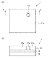
- (A) is a schematic plan view showing an example of the polarizing film of the present invention
- (b) is a sectional view taken along line XX of (a).
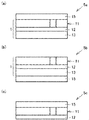
- 2A to 2C are schematic cross-sectional views showing an example of the circularly polarizing plate of the present invention.
- the polarizing film of the present invention has a liquid crystal cured layer, the liquid crystal cured layer contains a liquid crystal compound, and has at least a first region and a second region having mutually different values of visibility correction transmittance.
- the region is a region having a higher luminosity factor-corrected transmittance than the first region, and has a plan view shape of a circle, an ellipse, an ellipse, or a polygon, and the diameter when the second region is a circle is 2 cm or less.
- the major axis is 2 cm or less
- the second region is polygonal, a virtual circle drawn so that the polygon is inscribed.
- the diameter is 2 cm or less.
- FIG. 1(a) is a schematic plan view showing an example of the polarizing film of the present invention
- FIG. 1(b) is a sectional view taken along line XX of FIG. 1(a).
- the polarizing film 1 of the present embodiment is a film having a function of light absorption anisotropy, and has a liquid crystal cured layer 11 containing a liquid crystal compound.
- the liquid crystal cured layer 11 has at least two regions which are distinguished by the value of the visibility correction transmittance (Ty), and the at least two regions usually have different dichroic dye contents.
- the polarizing film 1 has the liquid crystal cured layer 11, but may further have a base material layer 13, an alignment layer 12, and other layers.
- the polarizing film 1 shown in FIG. 1B shows an example in which the alignment layer 12 and the liquid crystal cured layer 11 are provided on one side of the base material layer 13, but the alignment layer and the liquid crystal cured layer are provided on both sides of the base material layer 13. May have.
- the structures of the liquid crystal cured layers provided on both sides of the base material layer 13 may be the same as or different from each other.
- the polarizing film 1 may be a long polarizing film having a length of 10 m or more, and in this case, the polarizing film 1 can be a roll wound into a roll.
- the polarizing film can be continuously fed out from this wound body, and a process of laminating with a retardation layer, which will be described later, and cutting into individual sheets can be performed.
- the length of the long polarizing film used as the wound body is not particularly limited as long as it is 10 m or more, but can be, for example, 10000 m or less.
- the liquid crystal cured layer 11 contains a liquid crystal compound and has a region containing a liquid crystal compound and a dichroic dye.
- the dichroic dye and the liquid crystal compound have a region in a state of being horizontally aligned with respect to the polarizing film 1 plane.
- the dichroic dye and the liquid crystal compound have a region in a state of being horizontally aligned with respect to the plane of the polarizing film 1.
- the liquid crystal cured layer 11 contains a liquid crystal compound and usually further contains a dichroic dye.
- the region in which the dichroic dye and the liquid crystal compound are horizontally aligned with respect to the surface of the polarizing film is the absorbance A1( ⁇ ) in the liquid crystal alignment horizontal direction with respect to the light having the wavelength ⁇ nm and the liquid crystal alignment plane.
- the above ratio is about 5 to 10.
- the fact that the liquid crystal compound and the dichroic dye are not phase-separated means that, for example, surface observation by various microscopes or scattering degree measurement by a haze meter is performed. I can confirm.
- the liquid crystal cured layer 11 has a first region 11a and a second region 11b which are distinguished by the visibility correction transmittance.
- the polarizing film 1 shown in FIG. 1A shows an example in which two regions having different visibility correction transmittances are provided, but the first region and the second region may each be two or more. ..
- the first region 11a of the polarizing film 1 shown in FIG. 1(a) contains a liquid crystal compound and a dichroic dye.
- the second region 11b contains a liquid crystal compound, but may or may not contain a dichroic dye.
- the first region 11a contains a dichroic dye, its content is preferably higher than the content of the dichroic dye contained in the second region 11b.
- the content of the dichroic dye in the liquid crystal cured layer 11 can be determined by, for example, measuring the absorbance at the absorption maximum wavelength ( ⁇ MAX ) of the dichroic dye.
- the first region 11a has a higher visibility-corrected polarization degree value than the second region 11b.
- the first region 11a is preferably a region having high polarization characteristics, for example, the visibility correction polarization degree (Py) can be 90% or more, preferably 92% or more, and 95% or more. It is more preferable to be present, and usually 100% or less.
- the visibility correction transmittance (Ty) of the first region 11a can be set to, for example, 35% or more, preferably 40% or more, more preferably 42% or more, and usually less than 50%. ..
- the second region 11b is preferably a low polarization region having a visibility correction polarization degree (Py) lower than the visibility correction polarization degree (Py) of the first region 11a.
- the visibility correction polarization degree (Py) in the second region 11b may be, for example, 10% or less, preferably 5% or less, more preferably 1% or less, and even 0%. Good.
- the second region 11b has a visibility correction transmittance higher than that of the first region 11a.
- the second region 11b can have a visibility correction transmittance (Ty) of, for example, 80% or more, preferably 85% or more, more preferably 88% or more, and usually 98% or less. ..
- the visibility correction transmittance (Ty) and the visibility correction polarization degree (Py) in this specification can be calculated based on the polarization degree and the single transmittance measured by using a spectrophotometer.
- the transmittance of the transmittance of the transmission axis direction in the wavelength range of 380 nm ⁇ 780 nm is visible light (alignment vertical) (T 1) and the absorption axis direction (oriented the same direction) to (T 2)
- the spectrophotometer It can be measured by the double beam method using an apparatus in which a folder with a polarizer is set.
- the polarization degree and the single-body transmittance at each wavelength are calculated by using the following equations (Equation 1) and (Equation 2), and further, the 2 degree visual field (C of JIS Z 8701) is calculated.
- the luminosity correction polarization degree (Py) and the luminosity correction transmittance (Ty) can be calculated.
- the occupying area of the first region 11a and the occupying area of the second region 11b may be appropriately selected according to the characteristics required for the polarizing film 1.
- the ratio of the total area occupied by the first region 11a and the second region 11b to the surface area of the polarizing film 1 is preferably 90% or more, more preferably 95% or more, and more preferably 99% or more. Is more preferable.
- the occupied area of the first region 11a is preferably 50% or more, more preferably 70% or more, with respect to the total area of the occupied areas of the first region 11a and the second region 11b. It is more preferably 80% or more.
- the occupied area of the second region 11b may be smaller than the occupied area of the first region 11a, and the first region 11a may be provided so as to surround the second region 11b.
- the first region 11a is provided so as to surround one circular second region 11b, but a plurality of second regions 11b may be provided independently of each other.
- the shape of the first area 11a is not particularly limited.
- the first region 11a may have a plan view shape of a circle, an ellipse, an oval, a polygon, a line, a band, a wave, or the like.
- the second region 11b has a plan view shape of a circle, an ellipse, an oval, or a polygon.
- its diameter is 2 cm or less, preferably 1 cm or less, and more preferably 0.5 cm or less.
- its diameter may be 0.05 cm or more, or 0.1 cm or more.
- the second region 11b is elliptical or oval
- its major axis is 2 cm or less, preferably 1 cm or less, and more preferably 0.5 cm or less.
- the diameter may be 0.05 cm or more, or 0.1 cm or more.
- the diameter of a virtual circle drawn so that the polygon is inscribed is 2 cm or less, preferably 1 cm or less, and more preferably 0.5 cm or less. preferable.
- the diameter of the virtual circle may be 0.05 cm or more, or 0.1 cm or more.
- the second region 11b having the above-mentioned shape can be suitably used as a region corresponding to the lens position of a camera provided on a smartphone, a tablet, or the like.
- the second region 11b is colored in the second region 11b by setting the visibility correction single transmittance (Ty) to 80% or more and the visibility correction polarization degree (Py) to 10% or less. It is possible to improve the performance of the camera, since it is possible to obtain high transparency.
- a plurality of first areas 11a and second areas 11b may be provided alternately.
- the long polarizing film is usually cut into a predetermined size according to the application of the polarizing film, etc. It is preferable to set the arrangement of the first region 11a and the second region 11b in the long polarizing film so that the region 11a and the second region 11b are formed.
- the polarizing film after cutting is the polarizing film 1 shown in FIG. 1A
- a plurality of second regions are arranged at predetermined intervals in the length direction and/or the width direction of the elongated polarizing film. It is preferable to provide 11b.
- the thickness of the first region 11a in the liquid crystal cured layer 11 is preferably 0.5 ⁇ m or more, more preferably 1 ⁇ m or more, and preferably 5 ⁇ m or less, more preferably 3 ⁇ m or less. ..
- the thickness of the second region 11b in the liquid crystal cured layer 11 is preferably the same as that of the first region 11a, preferably 0.5 ⁇ m or more, more preferably 1 ⁇ m or more, and 5 ⁇ m or less. It is preferable that it is 3 ⁇ m or less.
- the thickness of the liquid crystal cured layer 11 can be measured by an interference film thickness meter, a laser microscope, a stylus film thickness meter, or the like.
- the thickness of the second region 11b may be smaller than that of the first region 11a, but the difference between the thickness of the first region 11a and the thickness of the second region 11b is preferably 2 ⁇ m or less, and 1 ⁇ m or less. It is more preferable that the thickness is 0.5 ⁇ m or less.
- liquid crystal compound A known liquid crystal compound can be used as the liquid crystal compound contained in the liquid crystal cured layer 11.
- the type of liquid crystal compound is not particularly limited, and a rod-shaped liquid crystal compound, a discotic liquid crystal compound, and a mixture thereof can be used.
- the liquid crystal compound may be a polymer liquid crystal compound, a polymerizable liquid crystal compound, or a mixture thereof.
- a polymerizable liquid crystal compound is preferably used as the liquid crystal compound.
- the hue of the polarizing film can be arbitrarily controlled, and the polarizing film can be significantly thinned. Further, since the polarizing film can be manufactured without performing stretching treatment, it is possible to obtain a non-stretchable polarizing film that does not undergo stretching relaxation by heat.
- Polymerizable liquid crystal compound means a compound having a polymerizable group and having liquid crystallinity.
- the polymerizable group means a group involved in the polymerization reaction, and is preferably a photopolymerizable group.
- the photopolymerizable group refers to a group that can participate in the polymerization reaction by an active radical or an acid generated from a photopolymerization initiator described later.
- Examples of the polymerizable group include vinyl group, vinyloxy group, 1-chlorovinyl group, isopropenyl group, 4-vinylphenyl group, acryloyloxy group, methacryloyloxy group, oxiranyl group and oxetanyl group.
- an acryloyloxy group a methacryloyloxy group, a vinyloxy group, an oxiranyl group or an oxetanyl group is preferable, and an acryloyloxy group is more preferable.
- the liquid crystallinity may be thermotropic liquid crystal or lyotropic liquid crystal, but when mixed with a dichroic dye as in the liquid crystal cured layer of the present embodiment, it is preferable to use thermotropic liquid crystal.
- the polymerizable liquid crystal compound when it is a thermotropic liquid crystal, it may be a thermotropic liquid crystal compound exhibiting a nematic liquid crystal phase or a thermotropic liquid crystal compound exhibiting a smectic liquid crystal phase.
- the liquid crystal cured layer 11 exhibits a polarization function as a polymer film obtained by a polymerization reaction
- the liquid crystal state of the polymerizable liquid crystal compound is preferably a smectic phase, which has a higher order from the viewpoint of higher performance.
- the smectic phase is more preferable.
- Higher order smectic liquid crystal compounds forming a smectic B phase, a smectic F phase or a smectic I phase are more preferred.
- the liquid crystal cured layer 11 formed by the polymerizable liquid crystal compound has such a higher order smectic phase
- a region having higher polarization performance can be formed in the liquid crystal cured layer 11.
- a Bragg peak derived from a higher-order structure such as a hexatic phase or a crystal phase is obtained in X-ray diffraction measurement.
- the first region preferably exhibits a Bragg peak in X-ray diffraction measurement.
- the Bragg peak is a peak derived from the periodic structure of molecular orientation, and a film having a periodic interval of 3 to 6 ⁇ can be obtained.
- the liquid crystal cured layer 11 contains a polymer obtained by polymerizing the polymerizable liquid crystal compound in the state of the smectic phase, for example, because higher polarization characteristics can be imparted to the first region 11a.
- the polymerizable liquid crystal compound may be a monomer, but may be an oligomer or a polymer in which a polymerizable group is polymerized.
- the polymerizable liquid crystal compound exhibits a nematic liquid crystal phase or a smectic liquid crystal phase can be confirmed, for example, as follows. After the composition for forming a polarizing film is applied to a substrate to form a coating film, the solvent contained in the coating film is removed by heat treatment under the condition that the polymerizable liquid crystal compound does not polymerize. Then, the liquid crystal phase developed by heating the coating film formed on the substrate to the isotropic phase temperature and gradually cooling it is inspected by texture observation with a polarization microscope, X-ray diffraction measurement or differential scanning calorimetry. To do.
- the polymerizable liquid crystal compound is not particularly limited as long as it is a liquid crystal compound having at least one (meth)acryloyl group, and a known polymerizable liquid crystal compound can be used, but a compound exhibiting smectic liquid crystallinity is preferable.
- a polymerizable liquid crystal compound include a compound represented by the following formula (A1) (hereinafter sometimes referred to as “polymerizable liquid crystal compound (A1)”).
- X 1 and X 2 each independently represent a divalent aromatic group or a divalent alicyclic hydrocarbon group, wherein the divalent aromatic group or the divalent alicyclic hydrocarbon is represented.
- the hydrogen atom contained in the group may be substituted with a halogen atom, an alkyl group having 1 to 4 carbon atoms, a fluoroalkyl group having 1 to 4 carbon atoms, an alkoxy group having 1 to 4 carbon atoms, a cyano group or a nitro group.
- the carbon atom constituting the divalent aromatic group or the divalent alicyclic hydrocarbon group may be substituted with an oxygen atom, a sulfur atom or a nitrogen atom.
- at least one of X 1 and X 2 is a 1,4-phenylene group which may have a substituent or a cyclohexane-1,4-diyl group which may have a substituent.
- Y 1 is a single bond or a divalent linking group.
- n is 1 to 3, and when n is 2 or more, a plurality of X 1's may be the same as or different from each other.
- X 2 may be the same as or different from any or all of the plurality of X 1 .
- a plurality of Y 1's may be the same as or different from each other. From the viewpoint of liquid crystallinity, n is preferably 2 or more.
- U 1 represents a hydrogen atom or a (meth)acryloyloxy group.
- U 2 represents a (meth)acryloyloxy group.
- W 1 and W 2 are, independently of each other, a single bond or a divalent linking group.
- V 1 and V 2 independently of each other represent an alkanediyl group having 1 to 20 carbon atoms which may have a substituent, and —CH 2 — constituting the alkanediyl group is —O—, It may be replaced with —CO—, —S— or NH—.
- X 1 and X 2 are independently of each other, preferably a 1,4-phenylene group which may have a substituent, or a substituent which may have a substituent.
- the 1,4-phenylene group which may have a substituent or the cyclohexane-1,4-diyl group which may have a substituent may have a methyl group or an ethyl group.
- examples thereof include an alkyl group having 1 to 4 carbon atoms such as a group and a butyl group, a cyano group, and a halogen atom such as a chlorine atom and a fluorine atom. It is preferably unsubstituted.
- the polymerizable liquid crystal compound (A1) has the formula (A1-1) in the formula (A1): -(X 1 -Y 1 -) n -X 2 -(A1-1) [In the formula, X 1 , Y 1 , X 2 and n each have the same meaning as described above. ] [Hereinafter referred to as partial structure (A1-1)]. ] Is preferably an asymmetric structure from the viewpoint of easily exhibiting smectic liquid crystallinity.
- Examples of the polymerizable liquid crystal compound (A1) in which the partial structure (A1-1) is an asymmetric structure include, for example, a polymerizable liquid crystal compound (A1) in which n is 1 and one X 1 and X 2 are different from each other. ) Is mentioned.
- n 2 and two Y 1 have the same structure as each other, two X 1 have the same structure as each other, and one X 2 has a structure different from these two X 1 liquid crystal compound (A1)
- X 1 to bind to W 1 of the two X 1 is a structure that is different from the other of X 1 and X 2, one another in the same structure as the other of X 1 and X 2
- the polymerizable liquid crystal compound (A1) is also included.
- a compound (A1) is mentioned.
- R a and R b each independently represent a hydrogen atom or an alkyl group having 1 to 4 carbon atoms.
- Y 1 is, -CH 2 CH 2 -, - more preferably COO- or a single bond, when a plurality of Y 1 are present, Y 1 which binds to X 2 is, -CH 2 CH 2 - or - More preferably CH 2 O—.
- X 1 and X 2 all have the same structure, it is preferable that there are two or more Y 1 which are bonding methods different from each other. When a plurality of Y 1 having different bonding methods are present, an asymmetric structure is formed, so that smectic liquid crystallinity tends to be exhibited.
- U 2 is a (meth)acryloyloxy group.
- U 1 is a hydrogen atom or a (meth)acryloyloxy group, preferably a (meth)acryloyloxy group. From the viewpoint of improving adhesion between layers and heat resistance of the polarizing film, it is preferable that both U 1 and U 2 are (meth)acryloyloxy groups.
- the (meth)acryloyloxy group may be in a polymerized state or an unpolymerized state, but is preferably an unpolymerized state.
- Examples of the alkanediyl group represented by V 1 and V 2 include a methylene group, ethylene group, propane-1,3-diyl group, butane-1,3-diyl group, butane-1,4-diyl group, pentane- 1,5-diyl group, hexane-1,6-diyl group, heptane-1,7-diyl group, octane-1,8-diyl group, decane-1,10-diyl group, tetradecane-1,14-diyl group Group and icosane-1,20-diyl group and the like.
- V 1 and V 2 are preferably alkanediyl groups having 2 to 12 carbon atoms, and more preferably alkanediyl groups having 6 to 12 carbon atoms.
- Examples of the substituent optionally possessed by the alkanediyl group include a cyano group and a halogen atom.
- the alkanediyl group is preferably unsubstituted, and is an unsubstituted linear alkanediyl group. Is more preferable.
- W 1 and W 2 are preferably a single bond, —O—, —S—, —COO— or —OCOO—, more preferably a single bond or —O—.
- the polymerizable liquid crystal compound is not particularly limited as long as it is a polymerizable liquid crystal compound having at least one (meth)acryloyl group, and a known polymerizable liquid crystal compound can be used, but it is preferable to exhibit smectic liquid crystallinity.
- the structure that easily exhibits smectic liquid crystallinity it is preferable that the structure has an asymmetric molecular structure, and specifically, a polymerizable structure having a structure represented by formulas (Aa) to (Ai) It is more preferable that the liquid crystal compound is a polymerizable liquid crystal compound exhibiting smectic liquid crystallinity.
- polymerizable liquid crystal compound examples include compounds represented by formulas (A-1) to (A-25).
- the polymerizable liquid crystal compound has a cyclohexane-1,4-diyl group
- the cyclohexane-1,4-diyl group is preferably a trans isomer.
- the polymerizable liquid crystal compound one kind may be used alone, or two or more kinds may be used in combination.
- the polymerizable liquid crystal compounds may be used alone or in combination in the liquid crystal cured layer 11.
- at least one kind is preferably a polymerizable liquid crystal compound, and more preferably two or more kinds are polymerizable liquid crystal compounds.
- the mixing ratio is usually 1:99 to 50:50, preferably 5:95 to 50:50, and preferably 10:90 to 50:50. Is more preferable.
- the polymerizable liquid crystal compound may be, for example, Lub et al. Recl. Trav. Chim. It can be produced by a known method described in Pays-Bas, 115, 321-328 (1996), Japanese Patent No. 4719156 or the like.
- the content of the polymerizable liquid crystal compound in the liquid crystal cured layer 11 is usually 50 to 99.5 parts by mass, preferably 60 to 99 parts by mass, based on 100 parts by mass of the solid content of the liquid crystal cured layer 11.
- the amount is more preferably 70 to 98 parts by mass, further preferably 80 to 97 parts by mass.
- the solid content refers to the total amount of components excluding the solvent from the liquid crystal cured layer-forming composition described below.
- the dichroic dye refers to a dye having a property that the absorbance in the major axis direction of a molecule and the absorbance in the minor axis direction of the molecule are different.
- the dichroic dye is a dye that aligns with the liquid crystal compound and exhibits dichroism, and the dichroic dye itself may have polymerizability or may have liquid crystallinity.
- the dichroic dye preferably has a property of absorbing visible light, and more preferably has a maximum absorption wavelength ( ⁇ MAX ) in the range of 380 to 680 nm.
- Examples of such a dichroic dye include an acridine dye, an oxazine dye, a cyanine dye, a naphthalene dye, an azo dye and an anthraquinone dye, and among them, an azo dye is preferable.
- Examples of the azo dyes include monoazo dyes, bisazo dyes, trisazo dyes, tetrakisazo dyes and stilbeneazo dyes, and the bisazo dyes or trisazo dyes are preferable.
- the dichroic dyes may be used alone or in combination of two or more, but in order to obtain absorption in the entire visible light range, it is preferable to combine three or more dichroic dyes. It is more preferable to combine more than one kind of azo dye.
- a 1 , A 2 and A 3 are each independently a 1,4-phenylene group which may have a substituent, a naphthalene-1,4-diyl group, or a substituent.
- Have. p represents an integer of 0 to 4. When p is 2 or more, each A 2 may be the same or different from each other.
- compound (I) a compound represented by (hereinafter sometimes referred to as "compound (I)").
- Substituents optionally possessed by the 1,4-phenylene group, naphthalene-1,4-diyl group and divalent heterocyclic group in A 1 , A 2 and A 3 include a methyl group, an ethyl group or a butyl group.
- the unsubstituted amino group is —NH 2 .
- the alkyl group having 1 to 6 carbon atoms include methyl group, ethyl group and hexyl group.
- Examples of the alkanediyl group having 2 to 8 carbon atoms include ethylene group, propane-1,3-diyl group, butane-1,3-diyl group, butane-1,4-diyl group, pentane-1,5-diyl group. , Hexane-1,6-diyl group, heptane-1,7-diyl group, octane-1,8-diyl group and the like.
- a 1 , A 2 and A 3 are independently of each other, hydrogen is substituted with a methyl group or a methoxy group.
- a 1,4-phenylene group or a divalent heterocyclic group is preferable, and p is preferably 0 or 1.
- p is 1 and at least two of the three structures of A 1 , A 2 and A 3 are 1,4-phenylene groups in that both the ease of molecular synthesis and high performance are achieved. More preferable.
- Examples of the divalent heterocyclic group include quinoline, thiazole, benzothiazole, thienothiazole, imidazole, benzimidazole, oxazole, and benzoxazole having two hydrogen atoms removed.
- a 2 is a divalent heterocyclic group, a structure having a molecular bond angle of substantially 180° is preferable, and specifically, benzothiazole, benzimidazole, and benzoxazole in which two 5-membered rings are condensed. The structure is more preferred.
- T 1 and T 2 are, independently of each other, electron withdrawing groups or electron emitting groups and preferably have different structures, and T 1 is an electron withdrawing group and T 2 is an electron emitting group, or It is further preferred that T 1 is an electron emitting group and T 2 is an electron withdrawing group.
- each of T 1 and T 2 independently represents an alkyl group having 1 to 4 carbon atoms, an alkoxy group having 1 to 4 carbon atoms, a cyano group, a nitro group, or an alkyl group having 1 to 6 carbon atoms.
- an amino group having two, or an amino group in which two substituted alkyl groups are bonded to each other to form an alkanediyl group having 2 to 8 carbon atoms, or a trifluoromethyl group is preferable, and among them, a smectic liquid crystal group is preferable.
- a smectic liquid crystal group is preferable.
- an alkyl group having 1 to 6 carbon atoms an alkoxy group having 1 to 6 carbon atoms, a cyano group
- An amino group having one or two alkyl groups having 1 to 6 carbon atoms, or an amino group in which two substituted alkyl groups are bonded to each other to form an alkanediyl group having 2 to 8 carbon atoms is preferable.
- B 1 to B 20 each independently represent a hydrogen atom, an alkyl group having 1 to 6 carbon atoms, an alkoxy group having 1 to 6 carbon atoms, a cyano group, It represents a nitro group, a substituted or unsubstituted amino group (the definition of the substituted amino group and the unsubstituted amino group is as described above), a chlorine atom or a trifluoromethyl group.
- B 2 , B 6 , B 9 , B 14 , B 18 and B 19 are preferably hydrogen atoms or methyl groups, and more preferably hydrogen atoms.
- N1 to n4 each independently represent an integer of 0 to 3.
- a plurality of B 2 may be the same or different
- a plurality of B 6 may be the same or different
- a plurality of B 9 may be the same or different
- the plurality of B 14 may be the same or different.
- the anthraquinone dye is preferably a compound represented by the formula (2-7).
- R 1 to R 8 each independently represent a hydrogen atom, —R x , —NH 2 , —NHR x , —NR x 2 , —SR x, or a halogen atom.
- R x represents an alkyl group having 1 to 4 carbon atoms or an aryl group having 6 to 12 carbon atoms.
- oxazine dye a compound represented by the formula (2-8) is preferable.
- R 9 to R 15 each independently represent a hydrogen atom, —R x , —NH 2 , —NHR x , —NR x 2 , —SR x, or a halogen atom.
- R x represents an alkyl group having 1 to 4 carbon atoms or an aryl group having 6 to 12 carbon atoms.
- acridine dye a compound represented by the formula (2-9) is preferable.
- R 16 to R 23 each independently represent a hydrogen atom, —R x , —NH 2 , —NHR x , —NR x 2 , —SR x, or a halogen atom.
- R x represents an alkyl group having 1 to 4 carbon atoms or an aryl group having 6 to 12 carbon atoms.
- the alkyl group having 1 to 4 carbon atoms represented by R x is a methyl group, an ethyl group, a propyl group or a butyl group.
- a pentyl group, a hexyl group, and the like, and the aryl group having 6 to 12 carbon atoms includes a phenyl group, a toluyl group, a xylyl group, a naphthyl group, and the like.
- cyanine dye a compound represented by the formula (2-10) and a compound represented by the formula (2-11) are preferable.
- D 1 and D 2 each independently represent a group represented by any one of formulas (2-10a) to (2-10d).
- n5 represents an integer of 1 to 3.
- D 3 and D 4 each independently represent a group represented by any one of the formulas (2-11a) to (2-11h).
- n6 represents an integer of 1 to 3.
- the content of the dichroic dye (the ratio of the total amount of plural kinds of dichroic pigments) is a region having polarization characteristics, such as the first region 11a of the liquid crystal cured layer 11. Is usually 0.1 to 30 parts by mass, preferably 1 to 20 parts by mass, and more preferably 3 to 15 parts by mass with respect to 100 parts by mass of the polymerizable liquid crystal compound. ..
- the second region 11b of the liquid crystal cured layer 11 usually has a lower dichroic dye content than the first region 11a of the liquid crystal cured layer 11.
- the polarizing film 1 may have a base material layer 13.
- the base material layer 13 can be used to support the alignment layer 12 and the liquid crystal cured layer 21 described later when the polarizing film 1 is manufactured, for example, as described later, and the liquid crystal cured layer of the polarizing film 1 can be used. It can be used to support 11.
- the base material layer 13 may be a glass base material or a resin base material, but is preferably a resin base material. From the viewpoint that the polarizing film 1 can be continuously manufactured, it is more preferable that the base material layer 13 is formed by unwinding a long resin base material wound in a roll shape.
- the resin base material is preferably a light-transmitting base material capable of transmitting visible light.
- the light-transmitting property means that the single factor of the luminosity correction is 80% or more for the light in the wavelength range of 380 to 780 nm.
- the thickness of the base material layer 13 is preferably thin, but if it is too thin, strength tends to decrease and workability tends to deteriorate.
- the thickness of the base material layer 13 is usually 5 ⁇ m to 300 ⁇ m, preferably 20 ⁇ m to 200 ⁇ m.
- the base material layer 13 may be provided in a peelable manner. For example, after the liquid crystal cured layer 11 of the polarizing film 1 is attached to a member forming a display device, a retardation layer described later, or the like, the polarizing film is formed. It may be peelable from No. 1.
- the resin constituting the resin substrate examples include polyolefins such as polyethylene and polypropylene; cyclic olefin resins such as norbornene polymers; polyvinyl alcohol; polyethylene terephthalate; polymethacrylic acid ester; polyacrylic acid ester; triacetyl cellulose, diacetyl cellulose and Cellulose ester such as cellulose acetate propionate; polyethylene naphthalate; polycarbonate; polysulfone; polyether sulfone; polyether ketone; polyphenylene sulfide and polyphenylene oxide;
- polyolefins such as polyethylene and polypropylene
- cyclic olefin resins such as norbornene polymers
- polyvinyl alcohol polyethylene terephthalate
- polymethacrylic acid ester polyacrylic acid ester
- triacetyl cellulose, diacetyl cellulose and Cellulose ester such as cellulose acetate propionate
- cellulose ester resin substrates examples include “Fujitack Film” (manufactured by Fuji Photo Film Co., Ltd.); “KC8UX2M”, “KC8UY” and “KC4UY” (all manufactured by Konica Minolta Opto Co., Ltd.). ..
- cyclic olefin resins examples include “Topas” (registered trademark) (manufactured by Ticona (Germany)), “Arton” (registered trademark) (manufactured by JSR Corporation), “ZEONOR” (registered trademark), Examples thereof include “ZEONEX” (registered trademark) (above, manufactured by Nippon Zeon Co., Ltd.) and “APEL” (registered trademark) (manufactured by Mitsui Chemicals, Inc.).
- Such a cyclic olefin resin can be formed into a resin base material by a known means such as a solvent casting method or a melt extrusion method.
- resin base material of a commercially available cyclic olefin resin It is also possible to use a resin base material of a commercially available cyclic olefin resin.
- resin base materials for commercially available cyclic olefin resins "ESCINA” (registered trademark), “SCA40” (registered trademark) (above, Sekisui Chemical Co., Ltd.), “Zeonor film” (registered trademark) (Optes stock Manufactured by the company) and "Arton Film” (registered trademark) (manufactured by JSR Corporation).
- the base material layer 13 may have a one-layer structure or a multi-layer structure of two or more layers. When the base material layer 13 has a multi-layer structure, each layer may be made of the same material or different materials.
- the base material layer 13 may have a quarter wave plate function. Since the base material layer 13 has a quarter wavelength plate function, a polarizing film having a circular polarizing plate function can be obtained by combining the base material layer 13 and the liquid crystal cured layer 11. This makes it possible to obtain a circularly polarizing plate without attaching a retardation layer having a quarter wave plate function to the polarizing film 1 separately from the base material layer 13.
- the liquid crystal cured layer 11 is made to have a half-wave plate function by using a member in which a layer having a half-wave plate function and a layer having a quarter-wave plate function are laminated.
- a circularly polarizing plate can be obtained by laminating on the layer side having.
- the circularly polarizing plate can also be formed by using a member in which a layer having a quarter wavelength plate function of reverse wavelength dispersion and a layer having a positive C plate function are laminated. Obtainable.
- the polarizing film 1 may have the alignment layer 12 on the base material layer 13, and the alignment layer 12 is disposed between the base material layer 13 and the liquid crystal cured layer 11.
- the alignment layer 12 can have an alignment control force for aligning the liquid crystal compound in the liquid crystal cured layer 11 laminated thereon in a desired direction.
- Alignment layer 12 facilitates liquid crystal alignment of the liquid crystal compound.
- the state of liquid crystal alignment such as horizontal alignment, vertical alignment, hybrid alignment, and tilt alignment changes depending on the properties of the alignment layer 12 and the liquid crystal compound, and the combination thereof can be arbitrarily selected.
- the alignment layer 12 is a material that develops horizontal alignment as an alignment regulating force
- the liquid crystal compound can form horizontal alignment or hybrid alignment.
- the alignment layer 12 is a material that exhibits vertical alignment
- the liquid crystal compound can form vertical alignment or tilt alignment.
- the expressions such as horizontal and vertical indicate the direction of the long axis of the aligned liquid crystal compound with reference to the plane of the polarizing film 1.
- vertical alignment means having the major axis of the aligned polymerizable liquid crystal in a direction perpendicular to the plane of the polarizing film 1.
- the term “perpendicular” as used herein means 90° ⁇ 20° with respect to the plane of the polarizing film 1. Since the polarizing film 1 preferably has the polarization property of the plane of the polarizing film 1, the alignment layer 12 is preferably formed using a material that exhibits horizontal alignment.
- the alignment regulating force of the alignment layer 12 can be arbitrarily adjusted depending on the surface condition and rubbing conditions, and when the alignment layer 12 is formed of a photo-alignment polymer. Can be arbitrarily adjusted depending on the polarized light irradiation condition and the like. Further, the liquid crystal alignment can be controlled by selecting the physical properties such as surface tension and liquid crystallinity of the polymerizable liquid crystal compound.
- the thickness of the alignment layer 12 is usually 10 nm to 5000 nm, preferably 10 nm to 1000 nm, and more preferably 30 nm to 300 nm.
- the alignment layer 12 formed between the base material layer 13 and the liquid crystal cured layer 11 is insoluble in the solvent used when forming the liquid crystal cured layer 11 on the alignment layer 12, and Those having heat resistance in heat treatment for removal and alignment of liquid crystals are preferable.
- the alignment layer 12 may be, for example, an alignment film made of an alignment polymer, a photo alignment film, or a groove alignment film.
- the alignment layer 12 is preferably a photo-alignment film because the alignment direction thereof can be easily controlled.
- polyamide or gelatin having an amide bond in the molecule polyimide having an imide bond in the molecule
- polyamic acid which is a hydrolyzate thereof polyvinyl alcohol, alkyl modified polyvinyl alcohol, polyacrylamide, polyoxazole, polyethylene.
- examples thereof include imine, polystyrene, polyvinylpyrrolidone, polyacrylic acid, and polyacrylic acid ester. Of these, polyvinyl alcohol is preferable.
- These oriented polymers may be used alone or in combination of two or more.
- composition for forming an alignment layer in the alignment layer forming step examples include an alignment polymer composition and a composition for forming a photo-alignment film described later.
- alignment layer forming step examples include the following steps.
- the orientation layer made of the orientation polymer is formed by, for example, applying a composition obtained by dissolving the orientation polymer in a solvent (hereinafter, also referred to as “orientation polymer composition”) to the substrate layer and removing the solvent. Alternatively, it can be obtained by applying the oriented polymer composition to the substrate layer, removing the solvent, and rubbing (rubbing method).
- a composition obtained by dissolving the orientation polymer in a solvent hereinafter, also referred to as “orientation polymer composition”
- it can be obtained by applying the oriented polymer composition to the substrate layer, removing the solvent, and rubbing (rubbing method).
- solvent used in the oriented polymer composition water; alcohol solvent such as methanol, ethanol, ethylene glycol, isopropyl alcohol, propylene glycol, methyl cellosolve, butyl cellosolve or propylene glycol monomethyl ether; ethyl acetate, butyl acetate, ethylene glycol methyl Ester solvents such as ether acetate, ⁇ -butyrolactone, propylene glycol methyl ether acetate or ethyl lactate; ketone solvents such as acetone, methyl ethyl ketone, cyclopentanone, cyclohexanone, methyl amyl ketone or methyl isobutyl ketone; fats such as pentane, hexane or heptane Group hydrocarbon solvent; aromatic hydrocarbon solvent such as toluene or xylene; nitrile solvent such as acetonitrile; ether solvent such as tetrahydr
- the content of the orienting polymer in the orienting polymer composition may be within the range in which the orienting polymer can be completely dissolved in the solvent, but is preferably 0.1 to 20% by mass in terms of solid content with respect to the solution. , 0.1 to 10 mass% is more preferable.
- a commercially available alignment film material may be used as it is as the alignment polymer composition.
- Examples of commercially available alignment film materials include Sanever (registered trademark) (manufactured by Nissan Chemical Industries, Ltd.) and Optomer (registered trademark) (manufactured by JSR Corporation).
- a coating method such as a spin coating method, an extrusion method, a gravure coating method, a die coating method, a bar coating method or an applicator method, or a printing method such as a flexo method is used.
- a known method such as a method can be used.
- a printing method such as a gravure coating method, a die coating method or a flexo method can be usually adopted as the coating method.
- a dry film of the oriented polymer is formed.
- the method for removing the solvent include a natural drying method, a ventilation drying method, a heat drying method and a reduced pressure drying method. Thereafter, the dry coating film can be brought into contact with a rotating rubbing roll around which a rubbing cloth is wrapped to form the alignment layer 12.
- the photo-alignment film is usually obtained by applying a composition containing a polymer or monomer having a photoreactive group and a solvent (hereinafter, may be referred to as "composition for forming photo-alignment film") to the base material layer. It can be obtained by irradiating the coating layer for an alignment layer thus formed with polarized light (preferably polarized UV).
- composition for forming photo-alignment film is more preferable in that the direction of the alignment regulating force can be arbitrarily controlled by selecting the polarization direction of the polarized light to be irradiated.
- Photoreactive group refers to a group that produces a liquid crystal alignment ability when irradiated with light. Specifically, it is one that causes a photoreaction that is the origin of the liquid crystal alignment ability, such as an orientation induction or isomerization reaction of molecules generated by irradiation of light, a dimerization reaction, a photocrosslinking reaction, or a photolysis reaction. is there.
- a photoreactive group those that cause a dimerization reaction or a photocrosslinking reaction are preferable in terms of excellent orientation.
- a chalcone group or a cinnamoyl group is preferable from the viewpoint of easy control of reactivity and the manifestation of alignment regulating force during photo-alignment.
- These groups may have a substituent such as an alkyl group, an alkoxy group, an aryl group, an allyloxy group, a cyano group, an alkoxycarbonyl group, a hydroxyl group, a sulfonic acid group or a halogenated alkyl group.
- the solvent for the composition for forming a photo-alignment film is preferably one that dissolves a polymer and a monomer having a photoreactive group, and examples of the solvent include the solvents mentioned as the solvent for the above-mentioned alignment polymer composition. Be done.
- the content of the polymer or monomer having a photoreactive group in the composition for forming a photoalignment film is appropriately adjusted depending on the kind of the polymer or monomer having the photoreactive group and the thickness of the photoalignment film to be produced.
- the content is preferably 0.2% by mass or more, and particularly preferably 0.3 to 10% by mass.
- a polymeric material such as polyvinyl alcohol or polyimide, or a photosensitizer may be contained within a range that does not significantly impair the characteristics of the photo-alignment film.
- the same method as the method for applying the above-mentioned alignment polymer composition to the base material layer 13 can be mentioned.
- Examples of the method for removing the solvent from the coated composition for forming a photo-alignment film include the same methods as the method for removing the solvent from the oriented polymer composition.
- the polarized light irradiation may be performed directly on the dry film, or may be performed from the base material layer side so that the dried film is irradiated with the polarized light transmitted through the base material layer.
- the polarized light used for polarized light irradiation is particularly preferably substantially parallel light.
- the wavelength of the polarized light to be irradiated is preferably in the wavelength range in which the photoreactive group of the polymer or monomer having a photoreactive group can absorb light energy. Specifically, UV (ultraviolet light) in the wavelength range of 250 to 400 nm is particularly preferable.
- Examples of the light source used for polarized light irradiation include xenon lamps, high-pressure mercury lamps, ultra-high-pressure mercury lamps, metal halide lamps, and ultraviolet lasers such as KrF and ArF.
- High-pressure mercury lamps, ultra-high-pressure mercury lamps or metal halide lamps are more preferable. .. These lamps are preferable because they have high emission intensity of ultraviolet light having a wavelength of 313 nm.
- Polarized light can be emitted by irradiating light from a light source through an appropriate polarizer.
- a polarizing filter, a polarizing prism such as Glan-Thompson or Glan-Taylor, or a wire grid type polarizer can be used.
- the groove alignment film is a film having an uneven pattern or a plurality of grooves (grooves) on the film surface.
- the liquid crystal molecules are placed on a film having a plurality of linear globbs arranged at equal intervals, the liquid crystal molecules are aligned in the direction along the groove.
- a method for obtaining the glube alignment film after exposure through an exposure mask having a pattern-shaped slit on the surface of the photosensitive polyimide film, a method of forming an uneven pattern by developing and rinsing, a plate having a groove on the surface
- a method of forming a layer of UV-curable resin before curing on a sheet-shaped master, and transferring the resin layer to a substrate and then curing, a plurality of UV-curable resin films before curing formed on the substrate examples include a method of pressing a roll-shaped master having grooves to form irregularities and then curing. Specific examples thereof include the methods described in JP-A-6-34976 and JP-A-2011-242743.
- the width of the convex portion of the glube alignment film is preferably 0.05 ⁇ m to 5 ⁇ m, the width of the concave portion is preferably 0.1 ⁇ m to 5 ⁇ m, and the unevenness
- the depth is preferably 2 ⁇ m or less, and more preferably 0.01 ⁇ m to 1 ⁇ m or less.
- the polarizing film 1 may have layers other than the base material layer 13 and the orientation layer 12.
- a protective film for the purpose of protecting the surface of the liquid crystal cured layer 11 may be provided on the surface of the liquid crystal cured layer 11 opposite to the base layer 13.
- a protective film may be provided on the surface of the liquid crystal cured layer 11 on the side where the base material layer 13 is peeled off.
- the protective film may have a single-layer structure or a multi-layer structure. When the protective film has a multilayer structure, each layer may be made of the same material or different materials.
- the method for producing a polarizing film of the present invention can be produced by preparing a liquid crystal cured layer and further providing a second region.
- the method for preparing the liquid crystal cured layer and the method for providing the second region are not particularly limited, but they are preferably manufactured by the method described in the manufacturing method described later.
- FIGS. 2(a) and 2(b) are schematic cross-sectional views showing an example of the circularly polarizing plate of the present invention.
- the polarizing film 1 shown in FIG. 1(b) is made into the circularly polarizing plates 5a, 5b shown in FIGS. 2(a) and 2(b) by laminating the retardation layer 15 having a quarter wavelength plate function.
- the retardation layer 15 may be laminated on the liquid crystal cured layer 11 side of the polarizing film 1 (FIG. 2A) or may be laminated on the base material layer 13 side (FIG. 2B).
- the circularly polarizing plate 5a shown in FIG. 2A can be used as the circularly polarizing plate 5c (FIG. 2C) obtained by removing the base material layer 13, and in this case, the alignment layer 12 together with the base material layer 13 can be used. May also be peeled off.
- the circularly polarizing plate may be a laminate of the polarizing film 1 and a retardation layer having a multilayer structure.
- a retardation layer having a multilayer structure a retardation layer in which a layer having a 1 ⁇ 2 wavelength plate function and a layer having a 1 ⁇ 4 wavelength plate function are laminated can be used.
- a circularly polarizing plate can be obtained by laminating the polarizing film 1 and the layer side having a half-wave plate function.
- a circularly polarizing plate is also obtained by using, as the retardation layer having a multi-layer structure, a retardation layer in which a layer having a quarter wavelength plate function of reverse wavelength dispersion and a layer having a positive C plate function are laminated. be able to.
- a material having a function as a retardation layer may be used as the base material layer 13 of the polarizing film 1, and a retardation layer may be further laminated to form a circularly polarizing plate.
- the function of the base layer 13 and the retardation layer as the retardation layer may be selected according to the laminated position of the base layer 13 and the retardation layer in the circularly polarizing plate.
- the polarizing film and the retardation layer can be laminated via an adhesive layer using a known adhesive or adhesive.
- the method for producing a polarizing film of the present invention includes a step of irradiating a laminated film having a liquid crystal cured layer and a base material layer with a laser having a wavelength of 300 nm to 800 nm, and a part of the liquid crystal cured layer is This is a method for producing a polarizing film having a dichroic dye content lower than that of the above region.
- the laminated film having the liquid crystal cured layer and the base material is not particularly limited as long as it has the liquid crystal cured layer on at least one side of the base material layer.
- the base material include a protective film described later.
- the protective film may be laminated not only as a base material but also on the side opposite to the base material of the liquid crystal cured layer.
- the laminated film having an alignment layer further comprises a step of applying the composition for forming an alignment layer on one surface of the base material layer to form the alignment layer, and a liquid crystal cured layer on the surface on which the alignment layer is further formed. It can be manufactured through a step of applying a forming composition to form a liquid crystal cured layer.
- the base material layer 13 may be surface-treated before applying the composition for forming an alignment layer.
- the surface treatment method include corona treatment, plasma treatment, laser treatment, ozone treatment, saponification treatment, flame treatment, coupling agent coating treatment, and primer treatment.
- the composition for forming an alignment layer the above-mentioned alignment polymer composition, the composition for forming a photo-alignment film, the composition containing a resin material for forming a glube alignment film, and the like can be used.
- the method for forming the alignment layer using each composition is also as described above.
- the alignment layer forming step is performed by irradiating the coating layer for an alignment layer formed by applying the composition for forming an alignment layer with polarized light.
- An alignment layer having an alignment regulating force in a predetermined direction can be formed.
- the composition for forming a liquid crystal cured layer is a composition containing a liquid crystal compound and a dichroic dye, and preferably contains a solvent and a polymerization initiator, and a sensitizer, a polymerization inhibitor, a leveling agent, a reactive additive. Etc. may be included.
- a solvent and a polymerization initiator and a sensitizer, a polymerization inhibitor, a leveling agent, a reactive additive. Etc. may be included.
- the liquid crystal compound and the dichroic dye those described above can be used.
- the solvent polymerization initiator, sensitizer, polymerization inhibitor, leveling agent, and reactive additive, those described below can be used.
- Examples of the method for applying the composition for forming a liquid crystal cured layer include an extrusion coating method, a direct gravure coating method, a reverse gravure coating method, a CAP coating method, a slit coating method, a micro gravure method, a die coating method and an inkjet method. Be done. Moreover, the method etc. which apply using a coater, such as a dip coater, a bar coater, and a spin coater, are also mentioned. Above all, when continuously coating in the Roll to Roll format, microgravure method, inkjet method, slit coating method, and die coating method are preferable, and when coating a single-wafer substrate such as glass. A highly uniform spin coating method is preferable.
- the composition for forming an alignment film or the like is applied to the base material layer to form an alignment layer, and the composition for forming a liquid crystal cured layer is continuously formed on the obtained alignment layer. It can also be applied to.
- the solvent is removed from the applied liquid crystal cured layer-formed composition to form the liquid crystal cured layer coating layer.
- the method for removing the solvent the same method as the method for removing the solvent from the oriented polymer composition can be used, and examples thereof include natural drying, ventilation drying, heat drying, reduced pressure drying, and a combination thereof. Be done. Of these, natural drying or heat drying is preferable.
- the drying temperature is preferably in the range of 0 to 200°C, more preferably in the range of 20 to 150°C, even more preferably in the range of 50 to 130°C.
- the drying time is preferably 10 seconds to 10 minutes, more preferably 30 seconds to 5 minutes.
- the coating layer for a liquid crystal cured layer formed in the liquid crystal cured layer forming step is irradiated with active energy rays to form a polymerizable liquid crystal compound. It is preferable to form a liquid crystal cured layer as a polymer layer of a polymerizable liquid crystal compound by photopolymerization.
- the type of the polymerizable liquid crystal compound contained in the coating layer for the liquid crystal cured layer (in particular, the type of photopolymerizable functional group contained in the polymerizable liquid crystal compound), in the case of containing a photopolymerization initiator It is appropriately selected depending on the type of photopolymerization initiator and the amount thereof. Specifically, one or more kinds of light selected from the group consisting of visible light, ultraviolet light, infrared light, X-rays, ⁇ rays, ⁇ rays, and ⁇ rays can be given. Among them, ultraviolet light is preferable because it is easy to control the progress of the polymerization reaction, and that widely used in the art as a photopolymerization device can be used. It is preferable to select the type of liquid crystal compound.
- a low pressure mercury lamp As a light source of active energy rays, a low pressure mercury lamp, a medium pressure mercury lamp, a high pressure mercury lamp, an ultrahigh pressure mercury lamp, a xenon lamp, a halogen lamp, a carbon arc lamp, a tungsten lamp, a gallium lamp, an excimer laser, a wavelength range of 380 to 440 nm
- a light source of active energy rays a low pressure mercury lamp, a medium pressure mercury lamp, a high pressure mercury lamp, an ultrahigh pressure mercury lamp, a xenon lamp, a halogen lamp, a carbon arc lamp, a tungsten lamp, a gallium lamp, an excimer laser, a wavelength range of 380 to 440 nm
- Examples thereof include an LED light source that emits light, a chemical lamp, a black light lamp, a microwave-excited mercury lamp, and a metal halide lamp.
- Irradiation intensity of the active energy rays are usually, 10mW / cm 2 ⁇ 3000mW / cm 2.
- the irradiation intensity of the active energy ray is preferably an intensity in a wavelength region effective for activating the cationic polymerization initiator or the radical polymerization initiator.
- the irradiation time of the active energy ray is usually 0.1 seconds to 10 minutes, preferably 0.1 seconds to 5 minutes, more preferably 0.1 seconds to 3 minutes, and further preferably 0.1. 1 second to 1 minute.
- the cumulative amount of light is, 10mJ / cm 2 ⁇ 3000mJ / cm 2, preferably 50mJ / cm 2 ⁇ 2,000mJ / cm 2, more preferably It can be 100 mJ/cm 2 to 1000 mJ/cm 2 . If the integrated light quantity is less than this range, the polymerizable liquid crystal compound may be insufficiently cured, and good transferability may not be obtained. On the contrary, when the integrated light quantity is above this range, the liquid crystal cured layer may be colored.
- the composition for forming a liquid crystal cured layer may contain a solvent.
- a solvent since the polymerizable liquid crystal compound has a high viscosity, when the polymerizable liquid crystal compound is used as the liquid crystal compound, the use of a composition for forming a liquid crystal cured layer containing a solvent facilitates coating, and as a result, a liquid crystal cured layer is formed. It is easy to form.
- the solvent those capable of completely dissolving the polymerizable liquid crystal compound and the dichroic dye are preferable. It is preferable that the solvent is inert to the polymerization reaction of the polymerizable liquid crystal compound.
- the solvent examples include alcohol solvents such as methanol, ethanol, ethylene glycol, isopropyl alcohol, propylene glycol, ethylene glycol methyl ether, ethylene glycol butyl ether or propylene glycol monomethyl ether; ethyl acetate, butyl acetate, ethylene glycol methyl ether acetate, ⁇ -butyrolactone.
- alcohol solvents such as methanol, ethanol, ethylene glycol, isopropyl alcohol, propylene glycol, ethylene glycol methyl ether, ethylene glycol butyl ether or propylene glycol monomethyl ether
- ethyl acetate, butyl acetate, ethylene glycol methyl ether acetate, ⁇ -butyrolactone examples of the solvent.
- ester solvents such as propylene glycol methyl ether acetate or ethyl lactate; ketone solvents such as acetone, methyl ethyl ketone, cyclopentanone, cyclohexanone, 2-heptanone or methyl isobutyl ketone; aliphatic hydrocarbon solvents such as pentane, hexane or heptane; toluene.
- an aromatic hydrocarbon solvent such as xylene, a nitrile solvent such as acetonitrile; an ether solvent such as tetrahydrofuran or dimethoxyethane; a chlorine-containing solvent such as chloroform or chlorobenzene; dimethylacetamide, dimethylformamide, N-methyl-2-pyrrolidone, Examples thereof include amide solvents such as 1,3-dimethyl-2-imidazolidinone. These solvents may be used alone or in combination of two or more.
- the content of the solvent contained in the composition for forming a liquid crystal cured layer is preferably 50 to 98 mass% with respect to the total amount of the composition for forming a liquid crystal cured layer.
- the solid content of the composition for forming a liquid crystal cured layer is preferably 2 to 50% by mass.
- the viscosity of the composition for forming a liquid crystal cured layer becomes low, so that the thickness of the liquid crystal cured layer layer 21 becomes substantially uniform and the liquid crystal cured layer layer 21 becomes uneven. Tend to occur.
- the content of the solid content can be determined in consideration of the thickness of the liquid crystal cured layer 21 to be manufactured.
- the composition for forming a liquid crystal cured layer may contain a polymerization initiator.
- the polymerization initiator can be used when a polymerizable liquid crystal compound is used as the liquid crystal compound, and is a compound capable of initiating a polymerization reaction such as the polymerizable liquid crystal compound.
- a photopolymerization initiator that generates an active radical by the action of light is preferable from the viewpoint of not depending on the phase state of the thermotropic liquid crystal.
- polymerization initiator examples include benzoin compounds, benzophenone compounds, alkylphenone compounds, acylphosphine oxide compounds, triazine compounds, iodonium salts or sulfonium salts.
- the benzoin compound may, for example, be benzoin, benzoin methyl ether, benzoin ethyl ether, benzoin isopropyl ether or benzoin isobutyl ether.
- benzophenone compound examples include benzophenone, methyl o-benzoylbenzoate, 4-phenylbenzophenone, 4-benzoyl-4′-methyldiphenyl sulfide, 3,3′,4,4′-tetra(tert-butylperoxycarbonyl)benzophenone And 2,4,6-trimethylbenzophenone and the like.
- alkylphenone compound examples include diethoxyacetophenone, 2-methyl-2-morpholino-1-(4-methylthiophenyl)propan-1-one, 2-benzyl-2-dimethylamino-1-(4-morpholinophenyl)butane.
- 1-one 2-hydroxy-2-methyl-1-phenylpropan-1-one, 1,2-diphenyl-2,2-dimethoxyethane-1-one, 2-hydroxy-2-methyl-1-[ 4-(2-hydroxyethoxy)phenyl]propan-1-one, 1-hydroxycyclohexylphenylketone or 2-hydroxy-2-methyl-1-[4-(1-methylvinyl)phenyl]propan-1-one
- Examples thereof include oligomers.
- acylphosphine oxide compound examples include 2,4,6-trimethylbenzoyldiphenylphosphine oxide and bis(2,4,6-trimethylbenzoyl)phenylphosphine oxide.
- triazine compound examples include 2,4-bis(trichloromethyl)-6-(4-methoxyphenyl)-1,3,5-triazine and 2,4-bis(trichloromethyl)-6-(4-methoxynaphthyl).
- polymerization initiator examples include Irgacure (registered trademark) 907, 184, 651, 819, 250, 369, 379, 127, 754, OXE01, OXE02, or OXE03 (manufactured by Ciba Specialty Chemicals Co., Ltd.).
- SEQUOL registered trademark
- BZ, Z, or BEE manufactured by Seiko Chemical Co., Ltd.
- kayacure registered trademark
- UVI-6992 manufactured by Dow Chemical Co., Ltd.
- ADEKA OPTOMER SP-152 N-1717, N-1919, SP-170, ADEKA ARCRULS NCI-831, ADEKA ARCRULS NCI-930 (manufactured by ADEKA Co., Ltd.); TAZ-A, or TAZ-PP (manufactured by Japan Siber Hegner Co., Ltd.); TAZ- 104 (manufactured by Sanwa Chemical Co., Ltd.); and the like.
- the polymerization initiator in the composition for forming a liquid crystal cured layer one kind may be used, or two or more kinds of polymerization initiators may be mixed and used according to the light source of light.
- the content of the polymerization initiator in the composition for forming a liquid crystal cured layer can be appropriately adjusted according to the type and amount of the polymerizable liquid crystal compound, but is usually 0 with respect to 100 parts by mass of the content of the polymerizable liquid crystal compound. 0.1 to 30 parts by mass, preferably 0.5 to 10 parts by mass, more preferably 0.5 to 8 parts by mass. When the content of the polymerization initiator is within the above range, the polymerization can be performed without disturbing the alignment of the polymerizable liquid crystal compound.
- the composition for forming a liquid crystal cured layer may contain a sensitizer.
- the sensitizer can be preferably used when a polymerizable liquid crystal compound is used as the liquid crystal compound.
- the sensitizer is preferably a photosensitizer.
- sensitizer examples include xanthone compounds such as xanthone and thioxanthone (eg, 2,4-diethylthioxanthone and 2-isopropylthioxanthone); anthracene compounds such as anthracene and alkoxy group-containing anthracene (dibutoxyanthracene); phenothiazine. Alternatively, rubrene and the like can be mentioned.
- the composition for forming a liquid crystal cured layer contains a sensitizer
- the polymerization reaction of the polymerizable liquid crystal compound contained in the composition for forming a liquid crystal cured layer can be further promoted.
- the amount of the sensitizer used is preferably 0.1 to 10 parts by mass, more preferably 0.5 to 5 parts by mass, and 0.5 to 3 parts by mass with respect to 100 parts by mass of the content of the polymerizable liquid crystal compound. Parts are more preferred.
- the composition for forming a liquid crystal cured layer may contain a polymerization inhibitor from the viewpoint of stably advancing the polymerization reaction.
- the polymerization inhibitor can be preferably used when a polymerizable liquid crystal compound is used as the liquid crystal compound, and the polymerization inhibitor can control the degree of progress of the polymerization reaction of the polymerizable liquid crystal compound.
- a radical scavenger such as hydroquinone, hydroquinone containing an alkoxy group, catechol containing an alkoxy group (butyl catechol, etc.), pyrogallol, 2,2,6,6-tetramethyl-1-piperidinyloxy radical; thio; Phenol compounds; ⁇ -naphthylamine compounds or ⁇ -naphthol compounds; and the like.
- the content of the polymerization inhibitor is preferably 0.1 to 10 parts by mass, more preferably 100 parts by mass of the content of the polymerizable liquid crystal compound. Is 0.5 to 5 parts by mass, more preferably 0.5 to 3 parts by mass. When the content of the polymerization inhibitor is within the above range, the polymerization can be performed without disturbing the alignment of the polymerizable liquid crystal compound.
- the composition for forming a liquid crystal cured layer may contain a leveling agent.
- the leveling agent is an additive having a function of adjusting the fluidity of the composition and making the film obtained by applying the composition more flat, for example, an organic modified silicone oil type, a polyacrylate type or a perfluoro type.
- Alkyl leveling agents may be mentioned. Specifically, DC3PA, SH7PA, DC11PA, SH28PA, SH29PA, SH30PA, ST80PA, ST86PA, SH8400, SH8700, FZ2123 (all manufactured by Toray Dow Corning Co., Ltd.), KP321, KP323, KP324, KP326, KP340.
- KP341, X22-161A, KF6001 (all manufactured by Shin-Etsu Chemical Co., Ltd.), TSF400, TSF401, TSF410, TSF4300, TSF4440, TSF4445, TSF-4446, TSF4452, TSF4460 (all above, Momentive Performance Materials Japan LLC) Fluorinert (registered trademark) FC-72, FC-40, FC-43, FC-3283 (all manufactured by Sumitomo 3M Ltd.), Megafac (registered trademark) R-08 , R-30, R-90, F-410, F-411, F-443, F-445, F-470, F-477, F-479, F-482.
- the composition for forming a liquid crystal cured layer contains a leveling agent, it is preferably 0.01 to 5 parts by mass, more preferably 0.1 to 5 parts by mass, still more preferably 100 parts by mass of the liquid crystal compound. Is 0.1 to 3 parts by mass.
- the content of the leveling agent is within the above range, it is easy to horizontally align the liquid crystal compound, and the resulting liquid crystal cured layer tends to be smoother.
- the content of the leveling agent with respect to the liquid crystal compound exceeds the above range, the resulting cured liquid crystal layer tends to have unevenness.
- the liquid crystal cured layer-forming composition may contain two or more leveling agents.
- the composition for forming a liquid crystal cured layer may contain a reactive additive.
- a reactive additive those having a carbon-carbon unsaturated bond and an active hydrogen reactive group in the molecule are preferable.
- the "active hydrogen-reactive group” referred to here is a group having reactivity with a group having active hydrogen such as a carboxyl group (-COOH), a hydroxyl group (-OH), and an amino group (-NH 2 ).
- a typical example thereof is a glycidyl group, an oxazoline group, a carbodiimide group, an aziridine group, an imide group, an isocyanate group, a thioisocyanate group, a maleic anhydride group and the like.
- the number of carbon-carbon unsaturated bonds or active hydrogen-reactive groups contained in the reactive additive is usually 1 to 20 and preferably 1 to 10 respectively.
- the reactive additive preferably has at least two active hydrogen-reactive groups, and in this case, the active hydrogen-reactive groups present in plural may be the same or different.
- the carbon-carbon unsaturated bond contained in the reactive additive may be a carbon-carbon double bond, a carbon-carbon triple bond, or a combination thereof, but a carbon-carbon double bond is preferable.
- the reactive additive preferably contains a carbon-carbon unsaturated bond as a vinyl group and/or a (meth)acrylic group.
- a reactive additive having an active hydrogen reactive group which is at least one selected from the group consisting of an epoxy group, a glycidyl group and an isocyanate group is preferable, and a reactive additive having an acryl group and an isocyanate group is more preferable. ..
- the reactive additive include compounds having a (meth)acrylic group and an epoxy group, such as methacryloxyglycidyl ether and acryloxyglycidyl ether; (meth)acrylic group and oxetane, such as oxetane acrylate and oxetane methacrylate.
- a compound having a group a compound having a (meth)acrylic group and a lactone group such as lactone acrylate and lactone methacrylate; a compound having a vinyl group and an oxazoline group such as vinyloxazoline and isopropenyloxazoline; isocyanatomethyl acrylate And an oligomer of a compound having a (meth)acryl group and an isocyanate group, such as isocyanatomethyl methacrylate, 2-isocyanatoethyl acrylate or 2-isocyanatoethyl methacrylate.
- a compound having a vinyl group or a vinylene group and an acid anhydride such as methacrylic acid anhydride, acrylic acid anhydride, maleic acid anhydride or vinyl maleic acid anhydride, may be mentioned.
- methacryloxy glycidyl ether, acryloxy glycidyl ether, isocyanatomethyl acrylate, isocyanatomethyl methacrylate, vinyl oxazoline, 2-isocyanatoethyl acrylate, 2-isocyanatoethyl methacrylate or the above oligomers are preferable, and isocyanatomethyl acrylate, 2-Isocyanatoethyl acrylate or the above oligomers are particularly preferred.
- a compound represented by the following formula (Y) is preferable.
- n represents an integer of 1 to 10
- R 1′ represents a divalent aliphatic or alicyclic hydrocarbon group having 2 to 20 carbon atoms or 2 having 5 to 20 carbon atoms. Represents a valent aromatic hydrocarbon group.
- Two R 2′ s in each repeating unit are —NH— and the other is a group represented by >NC( ⁇ O)—R 3′ .
- R 3′ represents a hydroxyl group or a group having a carbon-carbon unsaturated bond.
- R 3'Of at least one R 3' formula (Y) in R 3 is a carbon - is a group having a carbon unsaturated bond.
- the compound represented by the formula (YY) (hereinafter sometimes referred to as the compound (YY)) is particularly preferable (wherein n has the same meaning as described above). Is).
- YY a commercially available product can be used as it is or after purification if necessary.
- examples of commercially available products include Laromer (registered trademark) LR-9000 (manufactured by BASF).
- the content of the reactive additive is usually 0.01 to 10 parts by mass, preferably 0. 1 to 5 parts by mass.
- a protective film may be laminated on the liquid crystal cured layer obtained by the above method.
- the protective film is a transparent (preferably optically transparent) thermoplastic resin, such as a chain polyolefin resin (polypropylene resin or the like) or a cyclic polyolefin resin (norbornene resin or the like).
- a transparent (preferably optically transparent) thermoplastic resin such as a chain polyolefin resin (polypropylene resin or the like) or a cyclic polyolefin resin (norbornene resin or the like).
- Polyolefin resin Cellulose resin such as triacetyl cellulose and diacetyl cellulose; Polyester resin such as polyethylene terephthalate and polybutylene terephthalate; Polycarbonate resin; (Meth)acrylic resin such as methyl methacrylate resin; Polystyrene -Based resin; polyvinyl chloride-based resin; acrylonitrile-butadiene-styrene-based resin; acrylonitrile-styrene-based resin; polyvinyl acetate-based resin; polyvinylidene chloride-based resin; polyamide-based resin; polyacetal-based resin; modified polyphenylene ether-based resin; polysulfone
- the film may be a resin made of a resin, a polyether sulfone resin, a polyarylate resin, a polyamideimide resin, a polyimide resin, or the like.
- chain polyolefin resin polyethylene resin (polyethylene resin which is a homopolymer of ethylene or a copolymer mainly composed of ethylene), polypropylene resin (a polypropylene resin which is a homopolymer of propylene or propylene is mainly used)
- a copolymer composed of two or more kinds of chain olefins can be mentioned.
- Cyclic polyolefin resin is a general term for resins polymerized with cyclic olefin as a polymerized unit, and is described in, for example, JP-A-1-240517, JP-A-3-14882, and JP-A-3-122137. Resins.
- cyclic polyolefin resins include ring-opening (co)polymers of cyclic olefins, addition polymers of cyclic olefins, copolymers of cyclic olefins with chain olefins such as ethylene and propylene (typically Are random copolymers), graft polymers obtained by modifying these with unsaturated carboxylic acids or their derivatives, and their hydrides.
- norbornene-based resins using norbornene-based monomers such as norbornene and polycyclic norbornene-based monomers as the cyclic olefin are preferably used.
- the polyester-based resin is a resin having an ester bond other than the following cellulose ester-based resins, and is generally composed of a polycondensate of a polyvalent carboxylic acid or its derivative and a polyhydric alcohol.
- a divalent dicarboxylic acid or its derivative can be used, and examples thereof include terephthalic acid, isophthalic acid, dimethyl terephthalate, and dimethyl naphthalenedicarboxylate.
- a divalent diol can be used as the polyhydric alcohol, and examples thereof include ethylene glycol, propanediol, butanediol, neopentyl glycol, and cyclohexanedimethanol.
- a typical example of the polyester resin is polyethylene terephthalate, which is a polycondensate of terephthalic acid and ethylene glycol.
- the (meth)acrylic resin is a resin containing a compound having a (meth)acryloyl group as a main constituent monomer.
- Specific examples of the (meth)acrylic resin include, for example, poly(meth)acrylic acid ester such as polymethyl methacrylate; methyl methacrylate-(meth)acrylic acid copolymer; methyl methacrylate-(meth)acrylic acid.
- Ester copolymer methyl methacrylate-acrylic acid ester-(meth)acrylic acid copolymer; methyl (meth)acrylate-styrene copolymer (MS resin etc.); methyl methacrylate and alicyclic hydrocarbon group
- a copolymer with a compound having such a compound for example, methyl methacrylate-cyclohexyl methacrylate copolymer, methyl methacrylate-norbornyl (meth)acrylate copolymer, etc.
- a polymer having a poly(meth)acrylic acid C 1-6 alkyl ester as a main component such as methyl poly(meth)acrylate is used, and more preferably, methyl methacrylate is a main component (50 to 100). %, preferably 70 to 100% by weight) methyl methacrylate resin is used.
- Cellulose ester resin is an ester of cellulose and fatty acid.
- Specific examples of the cellulose ester-based resin include cellulose triacetate, cellulose diacetate, cellulose tripropionate, and cellulose dipropionate.
- these copolymers and those in which a part of the hydroxyl groups are modified with other substituents are also included.
- cellulose triacetate triacetyl cellulose is particularly preferable.
- Polycarbonate resin is an engineering plastic made of a polymer in which monomer units are bonded via a carbonate group.
- the thickness of the protective film is usually 1 to 100 ⁇ m, but is preferably 5 to 60 ⁇ m and more preferably 5 to 50 ⁇ m from the viewpoint of strength and handleability. When the thickness is within this range, the liquid crystal cured layer is mechanically protected and the liquid crystal cured layer does not shrink even when exposed to a humid heat environment, and stable optical characteristics can be maintained.
- the protective film can be attached to the liquid crystal cured layer via an adhesive layer, for example.
- an adhesive layer for example.
- a water-based adhesive, an active energy ray-curable adhesive or a thermosetting adhesive can be used, and preferably a water-based adhesive or an active energy ray-curable adhesive.
- water-based adhesive examples include an adhesive composed of a polyvinyl alcohol-based resin aqueous solution and a water-based two-component urethane-based emulsion adhesive. Above all, a water-based adhesive composed of a polyvinyl alcohol-based resin aqueous solution is preferably used.
- the polyvinyl alcohol-based resin examples include vinyl alcohol homopolymers obtained by saponifying polyvinyl acetate, which is a homopolymer of vinyl acetate, as well as copolymers of vinyl acetate and other monomers copolymerizable therewith.
- a polyvinyl alcohol-based copolymer obtained by saponifying a polymer, a modified polyvinyl alcohol-based polymer obtained by partially modifying a hydroxyl group thereof, or the like can be used.
- the water-based adhesive may contain a crosslinking agent such as an aldehyde compound (glyoxal or the like), an epoxy compound, a melamine compound, a methylol compound, an isocyanate compound, an amine compound, a polyvalent metal salt or the like.
- a drying step for removing water contained in the water-based adhesive after the liquid crystal cured layer and the protective film are bonded together it is preferable to carry out a drying step for removing water contained in the water-based adhesive after the liquid crystal cured layer and the protective film are bonded together.
- a curing step of curing at a temperature of 20 to 45° C., for example, may be provided.
- the active energy ray-curable adhesive is an adhesive containing a curable compound that is cured by irradiation with active energy rays such as ultraviolet rays, visible light, electron beams, and X-rays, and is preferably an ultraviolet ray curable adhesive agent. Is.
- the above-mentioned curable compound can be a cationically polymerizable curable compound or a radically polymerizable curable compound.
- the cationically polymerizable curable compound include epoxy compounds (compounds having one or more epoxy groups in the molecule) and oxetane compounds (one or more oxetane rings in the molecule). Or a combination thereof.
- the radical-polymerizable curable compound include a (meth)acrylic compound (compound having one or more (meth)acryloyloxy groups in the molecule) and a radical-polymerizable double bond. Other vinyl compounds or combinations thereof may be mentioned.
- the active energy ray-curable adhesive usually further contains a cationic polymerization initiator and/or a radical polymerization initiator for initiating a curing reaction of the curable compound.
- At least one of these bonding surfaces may be subjected to surface activation treatment in order to enhance the adhesiveness.
- surface activation treatment dry treatment such as corona treatment, plasma treatment, discharge treatment (glow discharge treatment, etc.), flame treatment, ozone treatment, UV ozone treatment, ionizing actinic ray treatment (ultraviolet treatment, electron beam treatment, etc.) Ultrasonic treatment using a solvent such as water or acetone, saponification treatment, and wet treatment such as anchor coating treatment can be mentioned.
- surface activation treatments may be performed alone or in combination of two or more.
- the adhesive for laminating these protective films may be the same kind of adhesive or different kinds of adhesive.
- the step of irradiating the laminated film with a laser having a wavelength of 300 nm to 800 nm can be performed in the following embodiments, for example.
- the above laser is not particularly limited, and a YAG laser, a YLF laser, a YVO4 laser, a solid-state laser such as a titanium sapphire laser, or the like can be used.
- the wavelength of the laser can be appropriately selected depending on the composition and thickness of the liquid crystal cured layer or the substrate to be irradiated, but it is preferably 350 nm or more, more preferably 400 nm or more.
- the preferable upper limit of the wavelength of the laser is preferably 750 nm, more preferably 700 nm.
- the protective film When irradiating the laminated film with laser, it is preferable to irradiate the liquid crystal cured layer with laser.
- the protective film When the protective film is irradiated with a laser, the protective film preferably has a laser wavelength transmittance of 20% or more on the laser irradiation side, and more preferably 50% or more.
- the irradiation condition of the laser beam can be appropriately selected depending on the composition and thickness of the liquid crystal cured layer or the substrate to be irradiated, the laser device and the like.
- the laser power is preferably 0. It is 0.3 W or more, more preferably 0.5 W or more, preferably 10 W or less, more preferably 5 W or less.
- the switch frequency is preferably 1000 Hz or higher, more preferably 15000 Hz or higher, preferably 1,000,000 Hz or lower, more preferably 300,000 Hz or lower.
- the scanning speed is preferably 100 mm/sec or more, more preferably 200 mm/sec or more, preferably 10000 mm/sec or less, preferably 5000 mm/sec or less.
- the manufacturing method of the polarizing film is preferably a roll-to-roll type, and can be continuously manufactured.
- a step of previously winding a laminate having a base material and a liquid crystal cured layer in a roll shape, conveying the laminate while unwinding, and laminating a protective film, and a laser irradiation step may be performed continuously.
- the protective film wound in a roll shape may be conveyed while being unrolled, the protective film may be laminated on the laminate, and the laminated film may be laminated to obtain a laminated film.
- the laser irradiation step the laser can be irradiated while continuously conveying the laminated film.
- the obtained polarizing film can be further wound into a roll to form a wound body.
- a polarizing film having a length of, for example, 10 m or more can be prepared.
- the method for producing a polarizing film of the present invention it is possible to continuously produce a polarizing film including an alignment layer forming step and a liquid crystal cured layer forming step. Furthermore, when including an alignment layer forming step, the base material layer wound into a roll is conveyed while being unwound, and the base material layer is continuously coated with the composition for forming an alignment layer by a coating device. The alignment layer may be formed. When the liquid crystal cured layer forming step is carried out continuously, the liquid crystal cured layer forming composition is formed on the surface of the base layer with an alignment layer on which the alignment layer is formed, while continuously transporting the base layer with an alignment layer. May be applied to form a liquid crystal cured layer.
- the circularly polarizing plate of the present invention can be produced by laminating the polarizing film of the present invention and a retardation layer.
- a long retardation layer having a length of 10 m or more is used as the retardation layer, and both are continuous. It is preferable to form a long laminate by laminating the long polarizing film and the long retardation layer while being transported to. At this time, it is preferable to apply a pressure-sensitive adhesive or an adhesive to at least one of the long polarizing film and the long retardation layer to laminate them.
- the method for producing a circularly polarizing plate of the present invention may have a step of cutting into a single sheet.
- the cutting step it is preferable to cut the long laminate in at least one of the length direction and the width direction of the long laminate. In this case, it is preferable to determine the cutting position in the long laminated body so that the second region of the liquid crystal cured layer is arranged at a predetermined position in the cut sheet.
- Luminance correction transmittance (Ty), luminosity correction polarization degree (Py) For each sample, the luminosity correction polarization degree (Ty) and the luminosity correction polarization degree (Py) were calculated by the following procedure.
- Example 1 (Production of Composition for Alignment Layer Formation) 2 parts of a polymer (1) having a number average molecular weight of 28,000 represented by the following chemical formula and 98 parts of o-xylene are mixed, and the resulting mixture is stirred at 80° C. for 1 hour to give a composition for forming an alignment layer. Obtained.
- composition for forming liquid crystal cured layer The following components were mixed and stirred at 80° C. for 1 hour to obtain a composition for forming a liquid crystal cured layer.
- dichroic dye the azo dye described in the example of JP-A-2013-101328 was used.
- a triacetyl cellulose film (KC4UY-TAC manufactured by Konica Minolta Co., Ltd., thickness 40 ⁇ m) as a base material layer was cut into a size of 50 ⁇ 50 mm, and its surface was subjected to corona treatment (AGF-B10, manufactured by Kasuga Denki Co., Ltd.).
- the base material layer had a luminosity correction transmittance (Ty) of 2% at 355 nm and a luminosity correction transmittance (Ty) of 532 nm of 92%.
- composition for forming an alignment layer was applied to the surface of the film subjected to the corona treatment using a bar coater and then dried for 1 minute in a drying oven set at 120° C. to obtain a coating layer for the alignment layer.
- a polarized UV irradiation device SPOT CURE SP-7; manufactured by Ushio Inc.
- SPOT CURE SP-7 is used to irradiate polarized UV on the coating layer for an alignment layer with an integrated light amount of 50 mJ/cm 2 (313 nm standard) to form an alignment layer. did.
- composition for forming a liquid crystal cured layer was applied onto the obtained alignment layer using a bar coater, and then dried in a drying oven set at 110° C. for 1 minute.
- the liquid crystal is irradiated with ultraviolet rays (in a nitrogen atmosphere, wavelength: 365 nm, accumulated light quantity at wavelength 365 nm: 1000 mJ/cm 2 ).
- a liquid crystal cured layer 1 in which a compound and a dichroic dye were aligned was formed to obtain a laminated film 1 having a substrate layer, an alignment layer and a liquid crystal cured layer in this order.
- the liquid crystal cured layer 1 in the laminated film 1 had a luminosity correction transmittance of 42% and a luminosity correction polarization degree of 98%.
- a polarizing film was obtained by irradiating the laminated film 1 with a laser of 355 nm with a laser marker manufactured by Keyence Corporation from the liquid crystal cured layer side at an output of 3.2 W, a switch frequency of 100000 Hz, and a scan speed of 1000 mm/sec.
- the region formed by laser irradiation was circular (diameter 10 mm), and the luminous efficiency correction transmittance was 86%. Furthermore, the appearance and hue of the region formed by the laser irradiation were visually observed. The results are shown in Table 1.
- Example 2 A polarizing film was prepared and observed in the same manner as in Example 1 except that the laser wavelength was changed to 532 nm. The results are shown in Table 1.
- Example 3 A polarizing film was prepared and observed in the same manner as in Example 2 except that the laser irradiation diameter was 1 mm. The results are shown in Table 1.
- Example 4 A polarizing film was prepared and observed in the same manner as in Example 2 except that the laser irradiation diameter was 3 mm. The results are shown in Table 1.
- Example 5 A polarizing film was prepared and observed in the same manner as in Example 2 except that the laser irradiation diameter was 20 mm. The results are shown in Table 1.
- Example 6 A polarizing film was prepared and observed in the same manner as in Example 1 except that the laser was irradiated from the base material layer (triacetyl cellulose film) side. The results are shown in Table 1.
- Example 7 A polarizing film was prepared and observed in the same manner as in Example 4 except that the laser was irradiated from the side of the base material layer (triacetyl cellulose film). The results are shown in Table 1.
- Comparative Example 1 A polarizing film was prepared and observed in the same manner as in Example 2 except that the following laminated film 2 was used. The results are shown in Table 1.
- a water-based adhesive was injected between the obtained liquid crystal cured layer and a triacetyl cellulose film (KC4UY-TAC manufactured by Konica Minolta Co., Ltd., thickness: 40 ⁇ m), and they were bonded by a nip roll. While maintaining the tension of the obtained bonded product at 430 N/m, it was dried at 60° C. for 2 minutes to obtain a laminated film 2 having a cycloolefin film as a protective film on one surface.
- a triacetyl cellulose film K4UY-TAC manufactured by Konica Minolta Co., Ltd., thickness: 40 ⁇ m
- the above water-based adhesive was prepared by adding 3 parts of a carboxyl group-modified polyvinyl alcohol (Kuraray Poval KL318; manufactured by Kuraray Co., Ltd.) to 100 parts of water, and a water-soluble polyamide epoxy resin (Sumiraz Resin 650; manufactured by Sumika Chemtex Co., Ltd.). 1.5 parts of an aqueous solution having a solid content concentration of 30%) was added.
- a polarizing film was prepared and observed in the same manner as in Example 1 except that the laser wavelength was changed to 1064 nm. The results are shown in Table 1.
- [Comparative Example 3] A polarizing film was prepared and observed in the same manner as in Example 2 except that the laser irradiation diameter was changed to 30 mm. The results are shown in Table 1.
- each of the polarizing films of Examples 1 to 7 had a transparent hue. That is, each of the polarizing films of Examples 1 to 7 had a region having a higher transparency than the region not irradiated with the laser (that is, a region having a high luminous efficiency correction transmittance). Therefore, in each of the polarizing films of Examples 1 to 7, it was found that the region not irradiated with laser corresponds to the first region and the region irradiated with laser corresponds to the second region. On the other hand, in Comparative Example 2, no region having a transparent hue was observed. Therefore, it was revealed that the polarizing film of the present invention cannot be obtained by the production method of Comparative Example 2.
Landscapes
- Physics & Mathematics (AREA)
- General Physics & Mathematics (AREA)
- Optics & Photonics (AREA)
- Engineering & Computer Science (AREA)
- Health & Medical Sciences (AREA)
- Manufacturing & Machinery (AREA)
- Ophthalmology & Optometry (AREA)
- Mechanical Engineering (AREA)
- Chemical & Material Sciences (AREA)
- Crystallography & Structural Chemistry (AREA)
- Polarising Elements (AREA)
Abstract
Description
[1] 液晶硬化層を有する偏光フィルムであって、
前記液晶硬化層は、液晶化合物を含み、視感度補正透過率の値が互いに異なる第1領域及び第2領域を少なくとも有し、
前記第2領域は、視感度補正透過率が第1領域より高い領域であって、平面視形状が円形、楕円形、長円形又は多角形であり、前記第2領域が円形である場合の直径は2cm以下であり、前記第2領域が楕円形又は長円形である場合の長径は2cm以下であり、前記第2領域が多角形である場合、前記多角形が内接されるように描いた仮想円の直径は2cm以下である
偏光フィルム。
[2] さらに基材層と前記基材層の少なくとも片面側に積層された配向層とを有し、
液晶硬化層は、前記配向層上に積層されている
[1]に記載の偏光フィルム。
[3] 配向層は光配向性ポリマーを含む[2]に記載の偏光フィルム。
[4] 液晶化合物は重合性液晶化合物を含む[1]~[3]のいずれか1つに記載の偏光フィルム。
[5] 第1領域は視感度補正偏光度の値が第2領域より高い[1]~[4]のいずれか1つに記載の偏光フィルム。
[6] 第1領域における視感度補正偏光度は90%以上である[1]~[5]のいずれか1つに記載の偏光フィルム。
[7] 第2領域における視感度補正偏光度は10%以下である[1]~[6]のいずれか1つに記載の偏光フィルム。
[8] 液晶硬化層は、更に二色性色素を含有する[1]~[7]のいずれか1つに記載の偏光フィルム。
[9] 第1領域は、二色性色素の含有率が第2領域よりも大きい[8]に記載の偏光フィルム。
[10] 第1領域における視感度補正単体透過率は35%以上である[1]~[9]のいずれか1つに記載の偏光フィルム。
[11] 第2領域における視感度補正単体透過率は80%以上である[1]~[10]のいずれか1つに記載の偏光フィルム。
[12] 第1領域は、X線回折測定においてブラッグピークを示す[1]~[11]のいずれか1つに記載の偏光フィルム。
[13] 基材層は1/4波長板機能を有する[2]~[12]のいずれか1つに記載の偏光フィルム。
[14] 偏光フィルムの長さは10m以上である[1]~[13]のいずれか1つに記載の偏光フィルム。
[15] [1]~[12]及び[14]のいずれか1つに記載の偏光フィルムと1/4波長板機能を有する位相差層とを積層してなる円偏光板。
[16] 二色性色素を含む液晶硬化層と基材層とを有する積層フィルムに対して300nm~800nmの波長のレーザーを照射する工程を含む、前記液晶硬化層において一部の領域が他の領域より二色性色素の含有率が低い偏光フィルムの製造方法。
[17] 積層フィルムは更に配向層を有しており、前記配向層は液晶硬化層に積層されている[16]に記載の偏光フィルムの製造方法。
[18] 二色性色素の含有率が低下した領域は、平面視形状が円形、楕円形、長円形又は多角形であり、前記領域が円形である場合の直径は、2cm以下であり、前記領域が楕円形又は長円形である場合の長径は、2cm以下であり、前記領域が多角形である場合、前記多角形が内接されるように描いた仮想円の直径は2cm以下である[16]または[17]に記載の偏光フィルムの製造方法。
[19] 前記液晶硬化層は重合性液晶化合物の重合体を含む[16]~[18]の何れか1つに記載の偏光フィルムの製造方法。
[20] 前記偏光フィルムは長さが10m以上である[16]~[19]の何れか1つに記載の偏光フィルムの製造方法。
[21] 液晶硬化層と基材層とを有する積層フィルムに対して300nm~800nmの波長のレーザーを照射する工程(1)と、
前記工程(1)により得られた偏光フィルムと、1/4波長板機能を有する位相差層とを積層する工程(2)とを含む
円偏光板の製造方法。
[22] 工程(1)は工程(2)の後に行われる[21]に記載の円偏光板の製造方法。
更に、本願発明の製造方法によれば、本発明の偏光フィルムを効率よく得ることができる。
図1(a)は、本発明の偏光フィルムの一例を示す概略平面図であり、図1(b)は、図1(a)のX-X断面図である。
液晶硬化層11は液晶化合物を含み、液晶化合物と二色性色素とを含有する領域を有する。偏光フィルム1が偏光フィルム1平面の偏光特性を有する場合、二色性色素と液晶化合物が偏光フィルム1平面に対して水平配向した状態にある領域を有することが好ましい。偏光フィルム1が偏光フィルム1の膜厚方向の偏光特性を有する場合、二色性色素と液晶化合物が偏光フィルム1平面に対して水平配向した状態にある領域を有することが好ましい。
第1領域11aは、視感度補正透過率(Ty)を例えば35%以上とすることができ、40%以上であることが好ましく、42%以上であることがより好ましく、通常50%未満である。
透過率[%]=(T1+T2)/2 (式2)
液晶硬化層11に含まれる液晶化合物としては、公知の液晶化合物を用いることができる。液晶化合物の種類は特に限定されず、棒状液晶化合物、円盤状液晶化合物、及びこれらの混合物を用いることができる。液晶化合物は、高分子液晶化合物であってもよく、重合性液晶化合物であってもよく、これらの混合物であってもよい。
[式(A1)中、
X1及びX2は、互いに独立して、2価の芳香族基又は2価の脂環式炭化水素基を表し、ここで、該2価の芳香族基又は2価の脂環式炭化水素基に含まれる水素原子は、ハロゲン原子、炭素数1~4のアルキル基、炭素数1~4のフルオロアルキル基、炭素数1~4のアルコキシ基、シアノ基又はニトロ基に置換されていてもよく、該2価の芳香族基又は2価の脂環式炭化水素基を構成する炭素原子が、酸素原子又は硫黄原子又は窒素原子に置換されていてもよい。ただし、X1及びX2のうち少なくとも1つは、置換基を有していてもよい1,4-フェニレン基又は置換基を有していてもよいシクロヘキサン-1,4-ジイル基である。
-(X1-Y1-)n-X2- (A1-1)
〔式中、X1、Y1、X2及びnはそれぞれ上記と同じ意味を示す。〕
で示される部分〔以下、部分構造(A1-1)と称する。〕が非対称構造であることが、スメクチック液晶性を発現し易い点で、好ましい。

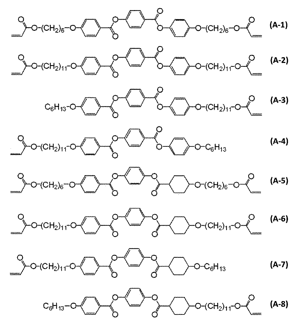


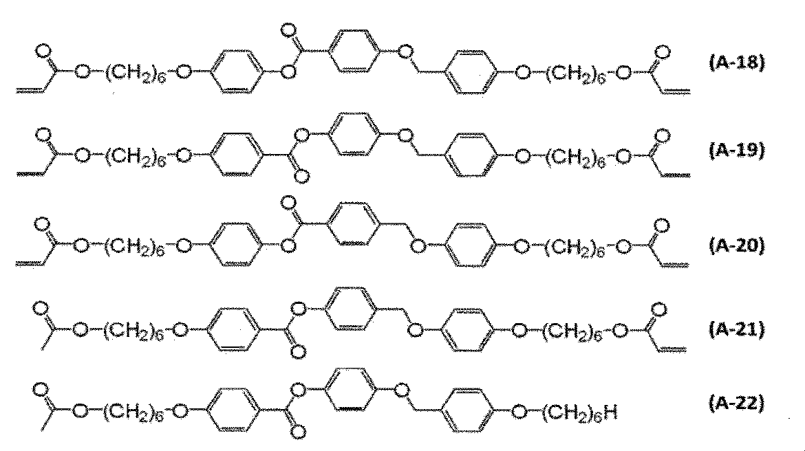
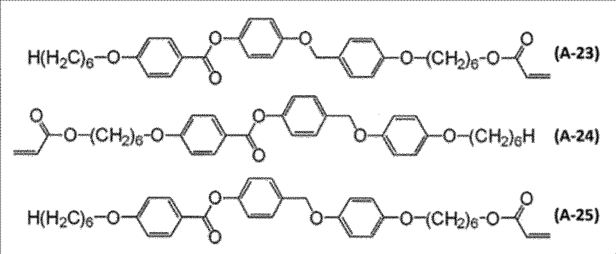
また、2種以上の重合性液晶化合物を組み合わせる場合には、少なくとも1種が重合性液晶化合物であることが好ましく、2種以上が重合性液晶化合物であることがより好ましい。2種以上の重合性液晶化合物を組み合わせることにより、液晶-結晶相転移温度以下の温度でも一時的に液晶性を保持することができる場合がある。2種類の重合性液晶化合物を組み合わせる場合の混合比としては、通常、1:99~50:50であり、5:95~50:50であることが好ましく、10:90~50:50であることがさらに好ましい。
二色性色素とは、分子の長軸方向における吸光度と、短軸方向における吸光度とが異なる性質を有する色素をいう。二色性色素は、液晶化合物とともに配向して二色性を示す色素であり、二色性色素自身が重合性を有していてもよいし、液晶性を有していてもよい。
二色性色素としては、可視光を吸収する特性を有する特性を有することが好ましく、380~680nmの範囲に吸収極大波長(λMAX)を有するものがより好ましい。このような二色性色素としては、例えば、アクリジン色素、オキサジン色素、シアニン色素、ナフタレン色素、アゾ色素又はアントラキノン色素等が挙げられるが、中でもアゾ色素が好ましい。アゾ色素としては、モノアゾ色素、ビスアゾ色素、トリスアゾ色素、テトラキスアゾ色素又はスチルベンアゾ色素等が挙げられ、好ましくはビスアゾ色素又はトリスアゾ色素である。二色性色素は単独で用いてもよく、2種以上を組み合わせて用いてもよいが、可視光全域で吸収を得るためには、3種類以上の二色性色素を組み合わせることが好ましく、3種類以上のアゾ色素を組み合わせることがより好ましい。
T1-A1(-N=N-A2)p-N=N-A3 -T2 (I)
[式(I)中、A1、A2及びA3は、互いに独立に、置換基を有していてもよい1,4-フェニレン基、ナフタレン-1,4-ジイル基、又は、置換基を有していてもよい2価の複素環基を表し、T1及びT2は、互いに独立に電子吸引基又は電子放出基であり、アゾ結合面内に対して実質的に180°の位置に有する。pは0~4の整数を表す。pが2以上である場合、各々のA2は互いに同一でも異なっていてもよい。可視域に吸収を示す範囲で-N=N-結合が-C=C-、-COO-、-NHCO-又は-N=CH-結合に置き換わっていてもよい。]
で表される化合物(以下、「化合物(I)」ということもある)が挙げられる。
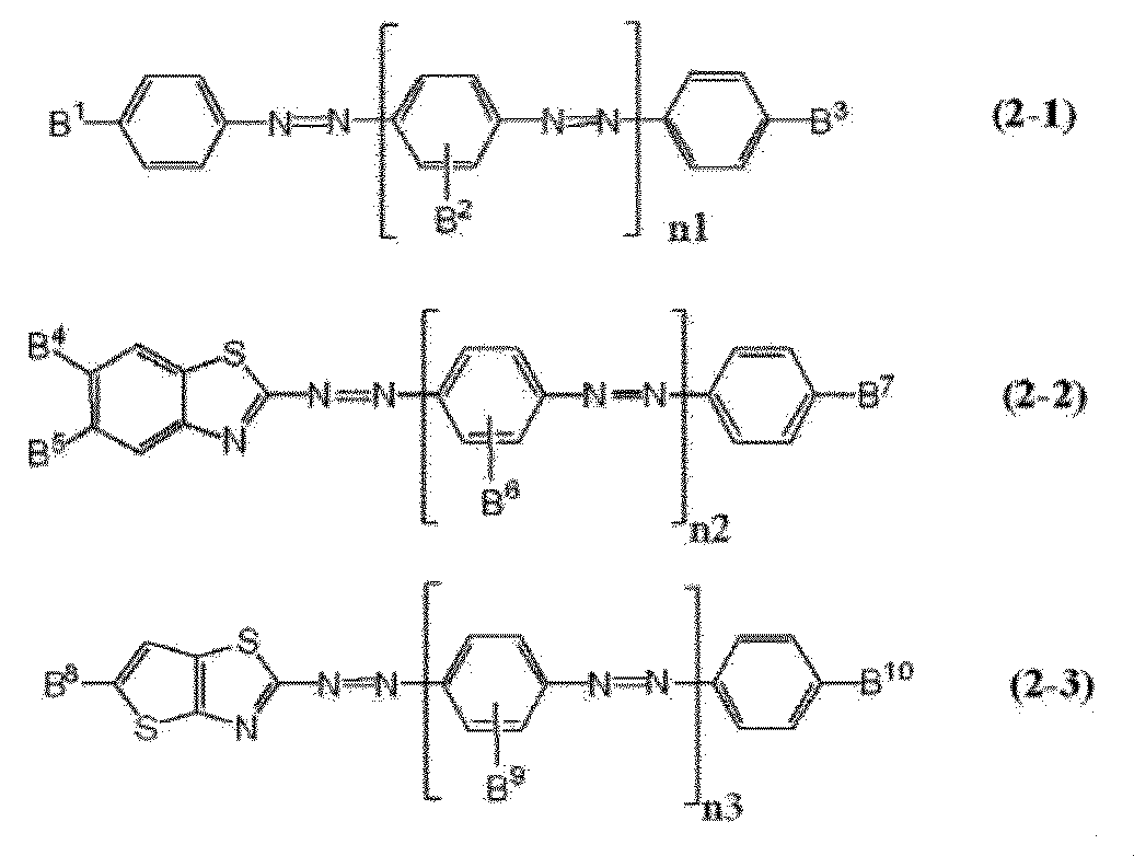
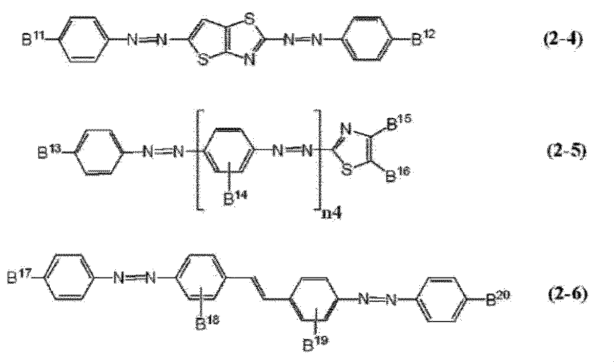
n2が2以上である場合、複数のB6はそれぞれ同一であってもよいし、異なっていてもよく、
n3が2以上である場合、複数のB9はそれぞれ同一であってもよいし、異なっていてもよく、
n4が2以上である場合、複数のB14はそれぞれ同一であってもよいし、異なっていてもよい。

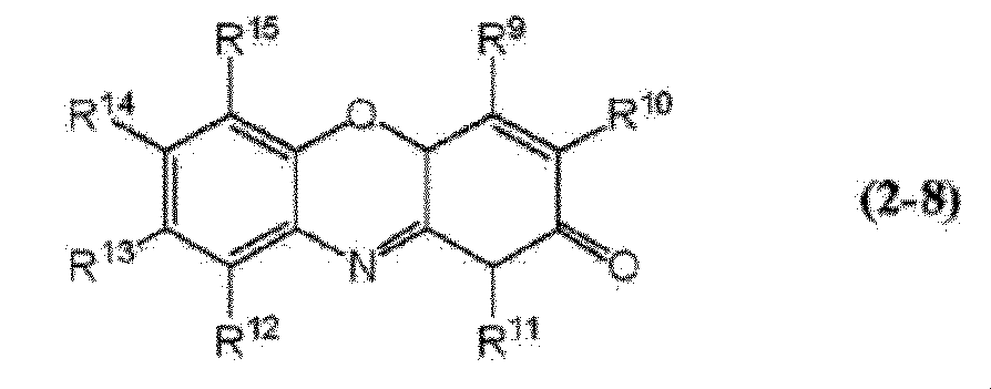
Rxは、炭素数1~4のアルキル基又は炭素数6~12のアリール基を表す。]

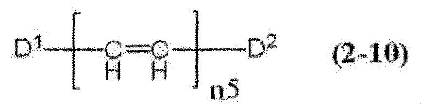
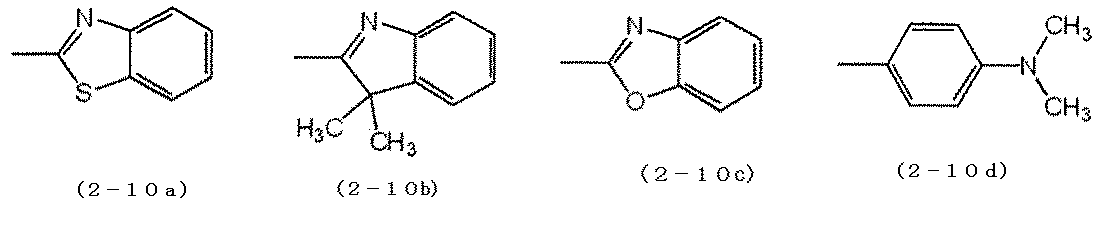
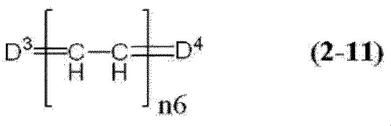

偏光フィルム1は、基材層13を有していてもよい。基材層13は、例えば後述するように、偏光フィルム1を製造する際に、配向層12や後述する液晶硬化層21を支持するために用いることができ、また、偏光フィルム1の液晶硬化層11を支持するために用いることができる。
偏光フィルム1は、基材層13上に配向層12を有していてもよく、配向層12は、基材層13と液晶硬化層11との間に配置される。配向層12は、その上に積層される液晶硬化層11中の液晶化合物を、所望の方向に液晶配向させる配向規制力を有することができる。
偏光フィルム1は、基材層13及び配向層12以外の層を有していてもよい。例えば、液晶硬化層11の基材層13とは反対側の面に、液晶硬化層11の表面を保護する等の目的の保護フィルムを設けてもよい。基材層13を剥離して用いる場合には、液晶硬化層11の基材層13を剥離した側の面に保護フィルムを設けてもよい。保護フィルムは1層構造であってもよく、多層構造であってもよい。保護フィルムが多層構造である場合、各層は同じ材料から形成されていてもよく、互いに異なる材料から形成されていてもよい。
図2(a)~(c)は、それぞれ本発明の円偏光板の一例を示す概略断面図である。図1(b)に示す偏光フィルム1は、1/4波長板機能を有する位相差層15を積層することにより、図2(a)及び(b)に示す円偏光板5a、5bとすることができる。位相差層15は、偏光フィルム1の液晶硬化層11側に積層してもよく(図2(a))、基材層13側に積層してもよい(図2(b))。図2(a)に示す円偏光板5aから、基材層13を剥離したものを円偏光板5c(図2(c))として用いることもでき、この場合、基材層13とともに配向層12も剥離してもよい。
この場合、多層構造の位相差層として、1/2波長板機能を有する層と1/4波長板機能を有する層とを積層した位相差層を用いることができ、多層構造の位相差層の1/2波長板機能を有する層側と偏光フィルム1とを積層することにより、円偏光板とすることができる。あるいは、多層構造の位相差層として、逆波長分散性の1/4波長板機能を有する層とポジティブCプレート機能を有する層とを積層した位相差層を用いることによっても、円偏光板を得ることができる。
基材としては、後述する保護フィルムが挙げられる。上記積層フィルムにおいて、保護フィルムは、基材として積層されるだけでなく、液晶硬化層の基材と反対側にも積層されていてよい。
例えば、配向層形成用組成物が光配向性ポリマーを含む場合、配向層形成工程は、配向層形成用組成物を塗工して形成された配向層用塗工層に偏光照射を行うことにより、所定の方向に配向規制力を有する配向層を形成することができる。
液晶硬化層形成用組成物は溶剤を含有していてもよい。一般に重合性液晶化合物は粘度が高いため、液晶化合物として重合性液晶化合物を用いる場合は、溶剤を含む液晶硬化層形成用組成物を用いることで塗工が容易になり、結果として液晶硬化層を形成しやすくなる。溶剤としては、重合性液晶化合物及び二色性色素を完全に溶解し得るものが好ましい。重合性液晶化合物の重合反応に不活性な溶剤であることが好ましい。
液晶硬化層形成用組成物は重合開始剤を含有していてもよい。重合開始剤は、液晶化合物として重合性液晶化合物を用いている場合に用いることができ、重合性液晶化合物等の重合反応を開始し得る化合物である。重合開始剤としては、サーモトロピック液晶の相状態に依存しないという観点から、光の作用により活性ラジカルを発生する光重合開始剤が好ましい。
液晶硬化層形成用組成物は増感剤を含有してもよい。増感剤は、液晶化合物として重合性液晶化合物を用いている場合に好適に用いることができる。光重合性基を有する重合性液晶化合物を用いている場合には、増感剤は光増感剤であることが好ましい。増感剤としては、例えば、キサントン及びチオキサントン等のキサントン化合物(例えば、2,4-ジエチルチオキサントン、2-イソプロピルチオキサントン等);アントラセン及びアルコキシ基含有アントラセン(ジブトキシアントラセン等)等のアントラセン化合物;フェノチアジン又はルブレン等が挙げられる。
液晶硬化層形成用組成物は、重合反応を安定的に進行させる観点から重合禁止剤を含有してもよい。重合禁止剤は、液晶化合物として重合性液晶化合物を用いている場合に好適に用いることができ、重合禁止剤により、重合性液晶化合物の重合反応の進行度合いをコントロールすることができる。
液晶硬化層形成用組成物はレベリング剤を含有してもよい。レベリング剤とは、組成物の流動性を調整し、組成物を塗布して得られる膜をより平坦にする機能を有する添加剤であり、例えば、有機変性シリコーンオイル系、ポリアクリレート系又はパーフルオロアルキル系のレベリング剤が挙げられる。具体的には、DC3PA、SH7PA、DC11PA、SH28PA、SH29PA、SH30PA、ST80PA、ST86PA、SH8400、SH8700、FZ2123(以上、全て東レ・ダウコーニング(株)製)、KP321、KP323、KP324、KP326、KP340、KP341、X22-161A、KF6001(以上、全て信越化学工業(株)製)、TSF400、TSF401、TSF410、TSF4300、TSF4440、TSF4445、TSF-4446、TSF4452、TSF4460(以上、全てモメンティブ パフォーマンス マテリアルズ ジャパン合同会社製)、フロリナート(fluorinert)(登録商標)FC-72、同FC-40、同FC-43、同FC-3283(以上、全て住友スリーエム(株)製)、メガファック(登録商標)R-08、同R-30、同R-90、同F-410、同F-411、同F-443、同F-445、同F-470、同F-477、同F-479、同F-482、同F-483(以上、いずれもDIC(株)製)、エフトップ(商品名)EF301、同EF303、同EF351、同EF352(以上、全て三菱マテリアル電子化成(株)製)、サーフロン(登録商標)S-381、同S-382、同S-383、同S-393、同SC-101、同SC-105、KH-40、SA-100(以上、全てAGCセイミケミカル(株)製)、商品名E1830、同E5844((株)ダイキンファインケミカル研究所製)、BM-1000、BM-1100、BYK-352、BYK-353又はBYK-361N(いずれも商品名:BM Chemie社製)等が挙げられる。中でも、ポリアクリレート系レベリング剤又はパーフルオロアルキル系レベリング剤が好ましい。
液晶硬化層形成用組成物は反応性添加剤を含んでもよい。反応性添加剤としては、その分子内に炭素-炭素不飽和結合と活性水素反応性基とを有するものが好ましい。なお、ここでいう「活性水素反応性基」とは、カルボキシル基(-COOH)、水酸基(-OH)、アミノ基(-NH2)等の活性水素を有する基に対して反応性を有する基を意味し、グリシジル基、オキサゾリン基、カルボジイミド基、アジリジン基、イミド基、イソシアネート基、チオイソシアネート基、無水マレイン酸基等がその代表例である。反応性添加剤が有する、炭素-炭素不飽和結合又は活性水素反応性基の個数は、通常、それぞれ1~20個であり、好ましくはそれぞれ1~10個である。
各繰返し単位にある2つのR2’は、一方が-NH-であり、他方が>N-C(=O)-R3’で示される基である。R3’は、水酸基又は炭素-炭素不飽和結合を有する基を表す。
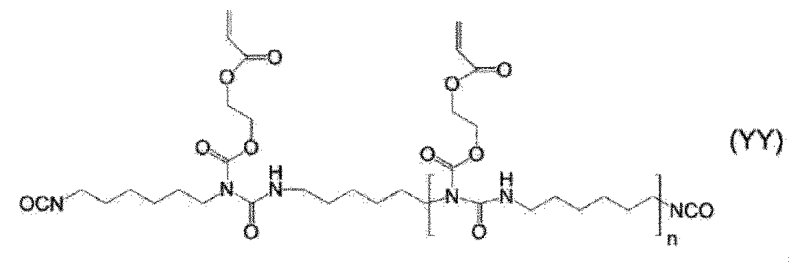
上記保護フィルムは、透光性を有する(好ましくは光学的に透明な)熱可塑性樹脂、例えば、鎖状ポリオレフィン系樹脂(ポリプロピレン系樹脂等)、環状ポリオレフィン系樹脂(ノルボルネン系樹脂等)のようなポリオレフィン系樹脂;トリアセチルセルロース、ジアセチルセルロースのようなセルロース系樹脂;ポリエチレンテレフタレート、ポリブチレンテレフタレートのようなポリエステル系樹脂;ポリカーボネート系樹脂;メタクリル酸メチル系樹脂のような(メタ)アクリル系樹脂;ポリスチレン系樹脂;ポリ塩化ビニル系樹脂;アクリロニトリル・ブタジエン・スチレン系樹脂;アクリロニトリル・スチレン系樹脂;ポリ酢酸ビニル系樹脂;ポリ塩化ビニリデン系樹脂;ポリアミド系樹脂;ポリアセタール系樹脂;変性ポリフェニレンエーテル系樹脂;ポリスルホン系樹脂;ポリエーテルスルホン系樹脂;ポリアリレート系樹脂;ポリアミドイミド系樹脂;ポリイミド系樹脂等からなるフィルムであることができる。
本発明において、積層フィルムに対して300nm~800nmの波長のレーザーを照射する工程は、例えば以下の実施態様にて行うことができる。
本発明の円偏光板は、本発明の偏光フィルムと位相差層とを積層することによって製造することができる。上記したように、偏光フィルムが連続的に製造された長さ10m以上の長尺偏光フィルムである場合、上記位相差層として、長さ10m以上の長尺位相差層を用い、両者を連続的に搬送しながら長尺偏光フィルムと長尺位相差層とを積層することにより、長尺積層体を形成することが好ましい。このとき、長尺偏光フィルム及び長尺位相差層の少なくとも一方に、粘着剤又は接着剤を塗工して両者を積層することが好ましい。
各サンプルについて、以下の手順で視感度補正偏光度(Ty)、視感度補正偏光度(Py)を算出した。
偏光度[%]={(T1-T2)/(T1+T2)}×100 (式2)
(配向層形成用組成物の製造)
下記化学式で表される数平均分子量28000のポリマー(1)2部とo-キシレン 98部とを混合し、得られた混合物を80℃で1時間攪拌することにより、配向層形成用組成物を得た。

下記の成分を混合し、80℃で1時間攪拌することにより、液晶硬化層形成用組成物を得た。二色性色素には、特開2013-101328号公報の実施例に記載のアゾ系色素を用いた。
・式(1-6)で表される重合性液晶化合物 75部
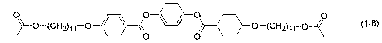
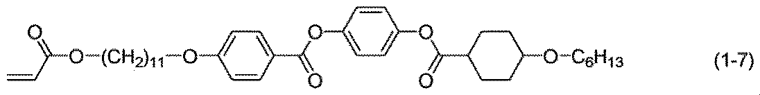
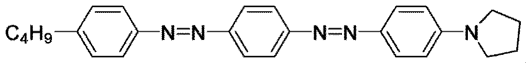

・レベリング剤:ポリアクリレート化合物(BYK-361N;BYK-Chemie社製) 1.2部
・溶剤:シクロペンタノン 250部
基材層としてのトリアセチルセルロースフィルム(コニカミノルタ社製KC4UY-TAC、厚さ40μm)を50×50mmに切り出し、その表面にコロナ処理(AGF-B10、春日電機株式会社製)を施した。
上記基材層は、355nmでの視感度補正透過率(Ty)が2%であり、532nm透過率での視感度補正透過率(Ty)が92%であった。
積層フィルム1に対して、液晶硬化層側からキーエンス社製レーザーマーカにて355nmのレーザーを出力3.2W、スイッチ周波数100000Hz、スキャンスピード1000mm/秒にて照射することにより偏光フィルムを得た。得られた偏光フィルムにおいて、レーザー照射により形成された領域は、円状(直径10mm)であり、視感度補正透過率が86%であった。更に、該レーザー照射により形成された領域の外観および色相を目視で観察した。その結果を表1に示す。
レーザーの波長を532nmに変更した以外は実施例1と同様に偏光フィルムを作成し、観察を行った。その結果を表1に示す。
〔実施例3〕
レーザーの照射径を1mmとした以外は実施例2と同様に偏光フィルムを作成し、観察を行った。その結果を表1に示す。
〔実施例4〕
レーザーの照射径を3mmとした以外は実施例2と同様に偏光フィルムを作成し、観察を行った。その結果を表1に示す。
〔実施例5〕
レーザーの照射径を20mmとした以外は実施例2と同様に偏光フィルムを作成し、観察を行った。その結果を表1に示す。
〔実施例6〕
レーザーを基材層(トリアセチルセルロースフィルム)側から照射したこと以外は実施例1と同様に偏光フィルムを作成し、観察を行った。その結果を表1に示す。
〔実施例7〕
レーザーを基材層(トリアセチルセルロースフィルム)側から照射したこと以外は実施例4と同様に偏光フィルムを作成し、観察を行った。その結果を表1に示す。
〔比較例1〕
下記積層フィルム2を用いた以外は実施例2と同様に偏光フィルムを作成し、観察を行った。その結果を表1に示す。
(積層フィルム2の製造)
厚さ30μmのポリビニルアルコールフィルム(平均重合度約2400、ケン化度99.9モル%以上)を、乾式延伸により約5倍に一軸延伸し、さらに緊張状態を保ったまま、40℃の純水に40秒間浸漬した。その後、ヨウ素/ヨウ化カリウム/水の質量比が0.044/5.7/100の染色水溶液に28℃で30秒間浸漬して染色処理を行った。
次に、ヨウ化カリウム/ホウ酸/水の質量比が11.0/6.2/100のホウ酸水溶液に70℃で120秒間浸漬した。引き続き、8℃の純水で15秒間洗浄した後、300Nの張力で保持した状態で、60℃で50秒間、次いで75℃で20秒間乾燥して、ポリビニルアルコールフィルムにヨウ素が吸着配向している厚さ12μmの液晶硬化層を得た。
得られた液晶硬化層と、トリアセチルセルロースフィルム(コニカミノルタ社製KC4UY-TAC、厚さ40μm)の間に水系接着剤を注入し、ニップロールで貼り合わせた。
得られた貼合物の張力を430N/mに保ちながら、60℃で2分間乾燥して、片面に保護フィルムとしてシクロオレフィンフィルムを有する積層フィルム2を得た。なお、上記水系接着剤は、水100部に、カルボキシル基変性ポリビニルアルコール(クラレポバール KL318;株式会社クラレ製)3部と、水溶性ポリアミドエポキシ樹脂(スミレーズレジン650;住化ケムテックス株式会社製、固形分濃度30%の水溶液)1.5部とを添加して調製した。
〔比較例2〕
レーザーの波長を1064nmに変更した以外は実施例1と同様に偏光フィルムを作成し、観察を行った。その結果を表1に示す。
〔比較例3〕
レーザーの照射径を30mmに変更した以外は実施例2と同様に偏光フィルムを作成し、観察を行った。その結果を表1に示す。

一方、比較例2では、透明の色相を有する領域が観察されなかった。よって、比較例2の製法では、本発明の偏光フィルムが得られないことがわかった。
Claims (22)
- 液晶硬化層を有する偏光フィルムであって、
前記液晶硬化層は、液晶化合物を含み、視感度補正透過率の値が互いに異なる第1領域及び第2領域を少なくとも有し、
前記第2領域は、視感度補正透過率が第1領域より高い領域であって、平面視形状が円形、楕円形、長円形又は多角形であり、前記第2領域が円形である場合の直径は2cm以下であり、前記第2領域が楕円形又は長円形である場合の長径は2cm以下であり、前記第2領域が多角形である場合、前記多角形が内接されるように描いた仮想円の直径は2cm以下である
偏光フィルム。 - さらに基材層と前記基材層の少なくとも片面側に積層された配向層とを有し、
液晶硬化層は、前記配向層上に積層されている
請求項1に記載の偏光フィルム。 - 配向層は光配向性ポリマーを含む請求項2に記載の偏光フィルム。
- 液晶化合物は重合性液晶化合物を含む請求項1~請求項3のいずれか1項に記載の偏光フィルム。
- 第1領域は視感度補正偏光度の値が第2領域より高い請求項1~請求項4のいずれか1項に記載の偏光フィルム。
- 第1領域における視感度補正偏光度は90%以上である請求項1~請求項5のいずれか1項に記載の偏光フィルム。
- 第2領域における視感度補正偏光度は10%以下である請求項1~請求項6のいずれか1項に記載の偏光フィルム。
- 液晶硬化層は、更に二色性色素を含有する請求項1~請求項7のいずれか1項に記載の偏光フィルム。
- 第1領域は、二色性色素の含有率が第2領域よりも大きい請求項8に記載の偏光フィルム。
- 第1領域における視感度補正単体透過率は35%以上である請求項1~請求項9のいずれか1項に記載の偏光フィルム。
- 第2領域における視感度補正単体透過率は80%以上である請求項1~請求項10のいずれか1項に記載の偏光フィルム。
- 第1領域は、X線回折測定においてブラッグピークを示す請求項1~請求項11のいずれか1項に記載の偏光フィルム。
- 基材層は1/4波長板機能を有する請求項2~請求項12のいずれか1項に記載の偏光フィルム。
- 偏光フィルムの長さは10m以上である請求項1~請求項13のいずれか1項に記載の偏光フィルム。
- 請求項1~請求項12及び請求項14のいずれか1項に記載の偏光フィルムと1/4波長板機能を有する位相差層とを積層してなる円偏光板。
- 二色性色素を含む液晶硬化層と基材層とを有する積層フィルムに対して300nm~800nmの波長のレーザーを照射する工程を含む、前記液晶硬化層において一部の領域が他の領域より二色性色素の含有率が低い偏光フィルムの製造方法。
- 積層フィルムは更に配向層を有しており、
前記配向層は液晶硬化層に積層されている
請求項16に記載の偏光フィルムの製造方法。 - 二色性色素の含有率が低下した領域は、平面視形状が円形、楕円形、長円形又は多角形であり、前記領域が円形である場合の直径は、2cm以下であり、前記領域が楕円形又は長円形である場合の長径は、2cm以下であり、前記領域が多角形である場合、前記多角形が内接されるように描いた仮想円の直径は2cm以下である請求項16又は請求項17に記載の偏光フィルムの製造方法。
- 前記液晶硬化層は重合性液晶化合物の重合体を含む請求項16~請求項18の何れか1項に記載の偏光フィルムの製造方法。
- 前記偏光フィルムは長さが10m以上である請求項16~請求項19の何れか1項に記載の偏光フィルムの製造方法。
- 二色性色素を有する液晶硬化層と基材とを有する積層フィルムに対して300nm~800nmの波長のレーザーを照射する工程(1)と、
前記工程(1)により得られた偏光フィルムと1/4波長板機能を有する位相差層とを積層する工程(2)とを含む
円偏光板の製造方法。 - 工程(1)は工程(2)の後に行われる請求項21に記載の円偏光板の製造方法。
Priority Applications (3)
| Application Number | Priority Date | Filing Date | Title |
|---|---|---|---|
| JP2020559954A JP7575275B2 (ja) | 2018-12-11 | 2019-12-04 | 偏光フィルム及びその製造方法 |
| CN201980081215.1A CN113167963B (zh) | 2018-12-11 | 2019-12-04 | 偏光膜及其制造方法 |
| KR1020217018808A KR102843442B1 (ko) | 2018-12-11 | 2019-12-04 | 편광 필름 및 그 제조 방법 |
Applications Claiming Priority (2)
| Application Number | Priority Date | Filing Date | Title |
|---|---|---|---|
| JP2018231608 | 2018-12-11 | ||
| JP2018-231608 | 2018-12-11 |
Publications (1)
| Publication Number | Publication Date |
|---|---|
| WO2020121907A1 true WO2020121907A1 (ja) | 2020-06-18 |
Family
ID=71075345
Family Applications (1)
| Application Number | Title | Priority Date | Filing Date |
|---|---|---|---|
| PCT/JP2019/047359 Ceased WO2020121907A1 (ja) | 2018-12-11 | 2019-12-04 | 偏光フィルム及びその製造方法 |
Country Status (5)
| Country | Link |
|---|---|
| JP (1) | JP7575275B2 (ja) |
| KR (1) | KR102843442B1 (ja) |
| CN (1) | CN113167963B (ja) |
| TW (1) | TWI908713B (ja) |
| WO (1) | WO2020121907A1 (ja) |
Cited By (1)
| Publication number | Priority date | Publication date | Assignee | Title |
|---|---|---|---|---|
| KR20230132696A (ko) | 2022-03-08 | 2023-09-18 | 스미또모 가가꾸 가부시끼가이샤 | 광학 적층체 및 그 제조 방법 |
Citations (3)
| Publication number | Priority date | Publication date | Assignee | Title |
|---|---|---|---|---|
| JP2014164084A (ja) * | 2013-02-25 | 2014-09-08 | Nitto Denko Corp | 偏光子および画像表示装置 |
| JP2017500606A (ja) * | 2014-03-26 | 2017-01-05 | エルジー・ケム・リミテッド | 局地的脱色領域を含む偏光部材、偏光部材ロールおよび枚葉型偏光部材の製造方法 |
| JP2018128573A (ja) * | 2017-02-08 | 2018-08-16 | 住友化学株式会社 | 偏光フィルム、円偏光板および表示装置 |
Family Cites Families (31)
| Publication number | Priority date | Publication date | Assignee | Title |
|---|---|---|---|---|
| KR960705248A (ko) * | 1994-07-15 | 1996-10-09 | 모리시다 요이치 | 헤드업 디스플레이 장치, 액정 디스플레이 패널 및 그 제조방법 |
| JP2005283846A (ja) * | 2004-03-29 | 2005-10-13 | Nitto Denko Corp | 光学フィルムおよび液晶表示装置 |
| JP2006119203A (ja) * | 2004-10-19 | 2006-05-11 | Nitto Denko Corp | 偏光板および偏光板の製造方法、ならびに、このような偏光板を用いた液晶パネル、液晶テレビおよび液晶表示装置 |
| CN100432785C (zh) * | 2004-12-08 | 2008-11-12 | 日东电工株式会社 | 液晶面板和液晶显示装置 |
| JP5000179B2 (ja) * | 2005-04-07 | 2012-08-15 | メルク パテント ゲゼルシャフト ミット ベシュレンクテル ハフツング | 配向膜 |
| JP2006337892A (ja) * | 2005-06-06 | 2006-12-14 | Nitto Denko Corp | 楕円偏光板、及び液晶パネル、及び液晶表示装置、及び画像表示装置 |
| JP2007025643A (ja) * | 2005-06-14 | 2007-02-01 | Fujifilm Corp | 偏光板、その加工製造方法及び液晶表示装置 |
| EP1816508A1 (en) * | 2006-02-02 | 2007-08-08 | Semiconductor Energy Laboratory Co., Ltd. | Display device |
| JP2009014843A (ja) * | 2007-07-02 | 2009-01-22 | Ricoh Co Ltd | 光路偏向素子、その製造方法および画像表示装置 |
| JP5525213B2 (ja) * | 2009-08-28 | 2014-06-18 | 富士フイルム株式会社 | 偏光膜、積層体、及び液晶表示装置 |
| JP5652011B2 (ja) * | 2010-06-10 | 2015-01-14 | 住友化学株式会社 | 光学フィルム |
| KR101989195B1 (ko) * | 2012-01-23 | 2019-06-13 | 스미또모 가가꾸 가부시키가이샤 | 조성물 및 광학 필름 |
| JP2014081482A (ja) * | 2012-10-16 | 2014-05-08 | Nitto Denko Corp | 偏光子および画像表示装置 |
| JP6076035B2 (ja) * | 2012-10-26 | 2017-02-08 | 住友化学株式会社 | 偏光性積層フィルムの製造方法及び偏光板の製造方法 |
| WO2014084687A1 (ko) * | 2012-11-29 | 2014-06-05 | 주식회사 엘지화학 | 광학 필름 |
| JP2014164085A (ja) * | 2013-02-25 | 2014-09-08 | Nitto Denko Corp | 偏光子および画像表示装置 |
| JP2014167547A (ja) * | 2013-02-28 | 2014-09-11 | Nitto Denko Corp | 画像表示装置の製造方法 |
| KR101678275B1 (ko) * | 2013-09-30 | 2016-11-21 | 주식회사 엘지화학 | 내츄럴 블랙에 근접한 편광판 제조 방법 및 이를 이용하여 제조된 편광판 |
| KR20150037550A (ko) * | 2013-09-30 | 2015-04-08 | 주식회사 엘지화학 | 국지적으로 편광 해소 영역을 갖는 편광판 및 그 제조 방법 |
| JP5753285B2 (ja) * | 2014-01-31 | 2015-07-22 | 株式会社巴川製紙所 | 光学積層体 |
| JP2015212823A (ja) | 2014-04-18 | 2015-11-26 | 住友化学株式会社 | パターン偏光フィルム |
| JP6299367B2 (ja) | 2014-04-18 | 2018-03-28 | 住友化学株式会社 | パターン偏光フィルムの製造方法 |
| KR102426386B1 (ko) * | 2014-04-18 | 2022-07-27 | 스미또모 가가꾸 가부시키가이샤 | 패턴 편광 필름 및 그의 제조 방법 |
| JP6152128B2 (ja) * | 2015-02-16 | 2017-06-21 | 日東電工株式会社 | 偏光子の製造方法 |
| JP6153642B2 (ja) * | 2015-05-13 | 2017-06-28 | 日東電工株式会社 | 偏光子の製造方法 |
| JP6152138B2 (ja) * | 2015-06-25 | 2017-06-21 | 日東電工株式会社 | 偏光子の製造方法 |
| JP6422415B2 (ja) * | 2015-09-28 | 2018-11-14 | 日東電工株式会社 | 偏光子、偏光板および画像表示装置 |
| JP6412476B2 (ja) * | 2015-09-28 | 2018-10-24 | 日東電工株式会社 | 偏光子、偏光板および画像表示装置 |
| JP6795883B2 (ja) * | 2015-10-05 | 2020-12-02 | 日東電工株式会社 | 偏光子の製造方法 |
| JP6634360B2 (ja) * | 2016-11-01 | 2020-01-22 | 日東電工株式会社 | 光学的表示装置の積層体、その製造方法および製造システム |
| KR102838251B1 (ko) * | 2017-01-05 | 2025-07-25 | 삼성디스플레이 주식회사 | 편광판 제조방법 및 편광판을 구비하는 표시장치 |
-
2019
- 2019-12-04 JP JP2020559954A patent/JP7575275B2/ja active Active
- 2019-12-04 WO PCT/JP2019/047359 patent/WO2020121907A1/ja not_active Ceased
- 2019-12-04 CN CN201980081215.1A patent/CN113167963B/zh active Active
- 2019-12-04 KR KR1020217018808A patent/KR102843442B1/ko active Active
- 2019-12-09 TW TW108144864A patent/TWI908713B/zh active
Patent Citations (3)
| Publication number | Priority date | Publication date | Assignee | Title |
|---|---|---|---|---|
| JP2014164084A (ja) * | 2013-02-25 | 2014-09-08 | Nitto Denko Corp | 偏光子および画像表示装置 |
| JP2017500606A (ja) * | 2014-03-26 | 2017-01-05 | エルジー・ケム・リミテッド | 局地的脱色領域を含む偏光部材、偏光部材ロールおよび枚葉型偏光部材の製造方法 |
| JP2018128573A (ja) * | 2017-02-08 | 2018-08-16 | 住友化学株式会社 | 偏光フィルム、円偏光板および表示装置 |
Cited By (3)
| Publication number | Priority date | Publication date | Assignee | Title |
|---|---|---|---|---|
| KR20230132696A (ko) | 2022-03-08 | 2023-09-18 | 스미또모 가가꾸 가부시끼가이샤 | 광학 적층체 및 그 제조 방법 |
| JP2023130873A (ja) * | 2022-03-08 | 2023-09-21 | 住友化学株式会社 | 光学積層体およびその製造方法 |
| US12393077B2 (en) | 2022-03-08 | 2025-08-19 | Sumitomo Chemical Company, Limited | Optical laminate and method of producing the optical laminate |
Also Published As
| Publication number | Publication date |
|---|---|
| TW202028787A (zh) | 2020-08-01 |
| JPWO2020121907A1 (ja) | 2021-10-28 |
| KR102843442B1 (ko) | 2025-08-06 |
| CN113167963A (zh) | 2021-07-23 |
| JP7575275B2 (ja) | 2024-10-29 |
| CN113167963B (zh) | 2023-08-11 |
| KR20210100639A (ko) | 2021-08-17 |
| TWI908713B (zh) | 2025-12-21 |
Similar Documents
| Publication | Publication Date | Title |
|---|---|---|
| JP7166049B2 (ja) | 楕円偏光板 | |
| JP7536938B2 (ja) | 偏光フィルム及び円偏光板 | |
| JP7684453B2 (ja) | 偏光フィルムおよびその製造方法 | |
| JP2021182144A (ja) | 複合偏光板および液晶表示装置 | |
| JP7198683B2 (ja) | 積層体 | |
| KR20230062548A (ko) | 광학 적층체 및 이것을 포함하는 타원 편광판 | |
| KR20240005687A (ko) | 적층체 및 표시 장치 | |
| JP7287896B2 (ja) | 偏光フィルムの製造方法及び偏光フィルム | |
| JP7272957B2 (ja) | 偏光フィルムの製造方法及び偏光フィルム | |
| KR20210038423A (ko) | 적층체 | |
| JP7575275B2 (ja) | 偏光フィルム及びその製造方法 | |
| KR20210127941A (ko) | 적층체, 및 화상 표시 장치 | |
| WO2020170697A1 (ja) | 積層体、及び画像表示装置 | |
| JP2025058922A (ja) | 積層体および表示装置 |
Legal Events
| Date | Code | Title | Description |
|---|---|---|---|
| 121 | Ep: the epo has been informed by wipo that ep was designated in this application |
Ref document number: 19895444 Country of ref document: EP Kind code of ref document: A1 |
|
| ENP | Entry into the national phase |
Ref document number: 2020559954 Country of ref document: JP Kind code of ref document: A |
|
| NENP | Non-entry into the national phase |
Ref country code: DE |
|
| ENP | Entry into the national phase |
Ref document number: 20217018808 Country of ref document: KR Kind code of ref document: A |
|
| 122 | Ep: pct application non-entry in european phase |
Ref document number: 19895444 Country of ref document: EP Kind code of ref document: A1 |