WO2020129558A1 - 誘電体多層膜、その製造方法及びそれを用いた光学部材 - Google Patents
誘電体多層膜、その製造方法及びそれを用いた光学部材 Download PDFInfo
- Publication number
- WO2020129558A1 WO2020129558A1 PCT/JP2019/046288 JP2019046288W WO2020129558A1 WO 2020129558 A1 WO2020129558 A1 WO 2020129558A1 JP 2019046288 W JP2019046288 W JP 2019046288W WO 2020129558 A1 WO2020129558 A1 WO 2020129558A1
- Authority
- WO
- WIPO (PCT)
- Prior art keywords
- layer
- refractive index
- multilayer film
- dielectric multilayer
- pores
- Prior art date
- Legal status (The legal status is an assumption and is not a legal conclusion. Google has not performed a legal analysis and makes no representation as to the accuracy of the status listed.)
- Ceased
Links
Images




















Classifications
-
- B—PERFORMING OPERATIONS; TRANSPORTING
- B01—PHYSICAL OR CHEMICAL PROCESSES OR APPARATUS IN GENERAL
- B01J—CHEMICAL OR PHYSICAL PROCESSES, e.g. CATALYSIS OR COLLOID CHEMISTRY; THEIR RELEVANT APPARATUS
- B01J23/00—Catalysts comprising metals or metal oxides or hydroxides, not provided for in group B01J21/00
- B01J23/16—Catalysts comprising metals or metal oxides or hydroxides, not provided for in group B01J21/00 of arsenic, antimony, bismuth, vanadium, niobium, tantalum, polonium, chromium, molybdenum, tungsten, manganese, technetium or rhenium
- B01J23/20—Vanadium, niobium or tantalum
-
- G—PHYSICS
- G02—OPTICS
- G02B—OPTICAL ELEMENTS, SYSTEMS OR APPARATUS
- G02B1/00—Optical elements characterised by the material of which they are made; Optical coatings for optical elements
- G02B1/10—Optical coatings produced by application to, or surface treatment of, optical elements
- G02B1/18—Coatings for keeping optical surfaces clean, e.g. hydrophobic or photo-catalytic films
-
- B—PERFORMING OPERATIONS; TRANSPORTING
- B01—PHYSICAL OR CHEMICAL PROCESSES OR APPARATUS IN GENERAL
- B01J—CHEMICAL OR PHYSICAL PROCESSES, e.g. CATALYSIS OR COLLOID CHEMISTRY; THEIR RELEVANT APPARATUS
- B01J21/00—Catalysts comprising the elements, oxides, or hydroxides of magnesium, boron, aluminium, carbon, silicon, titanium, zirconium, or hafnium
- B01J21/06—Silicon, titanium, zirconium or hafnium; Oxides or hydroxides thereof
- B01J21/063—Titanium; Oxides or hydroxides thereof
-
- B—PERFORMING OPERATIONS; TRANSPORTING
- B01—PHYSICAL OR CHEMICAL PROCESSES OR APPARATUS IN GENERAL
- B01J—CHEMICAL OR PHYSICAL PROCESSES, e.g. CATALYSIS OR COLLOID CHEMISTRY; THEIR RELEVANT APPARATUS
- B01J21/00—Catalysts comprising the elements, oxides, or hydroxides of magnesium, boron, aluminium, carbon, silicon, titanium, zirconium, or hafnium
- B01J21/06—Silicon, titanium, zirconium or hafnium; Oxides or hydroxides thereof
- B01J21/08—Silica
-
- B—PERFORMING OPERATIONS; TRANSPORTING
- B01—PHYSICAL OR CHEMICAL PROCESSES OR APPARATUS IN GENERAL
- B01J—CHEMICAL OR PHYSICAL PROCESSES, e.g. CATALYSIS OR COLLOID CHEMISTRY; THEIR RELEVANT APPARATUS
- B01J35/00—Catalysts, in general, characterised by their form or physical properties
- B01J35/19—Catalysts containing parts with different compositions
-
- B—PERFORMING OPERATIONS; TRANSPORTING
- B01—PHYSICAL OR CHEMICAL PROCESSES OR APPARATUS IN GENERAL
- B01J—CHEMICAL OR PHYSICAL PROCESSES, e.g. CATALYSIS OR COLLOID CHEMISTRY; THEIR RELEVANT APPARATUS
- B01J35/00—Catalysts, in general, characterised by their form or physical properties
- B01J35/30—Catalysts, in general, characterised by their form or physical properties characterised by their physical properties
-
- B—PERFORMING OPERATIONS; TRANSPORTING
- B01—PHYSICAL OR CHEMICAL PROCESSES OR APPARATUS IN GENERAL
- B01J—CHEMICAL OR PHYSICAL PROCESSES, e.g. CATALYSIS OR COLLOID CHEMISTRY; THEIR RELEVANT APPARATUS
- B01J35/00—Catalysts, in general, characterised by their form or physical properties
- B01J35/30—Catalysts, in general, characterised by their form or physical properties characterised by their physical properties
- B01J35/39—Photocatalytic properties
-
- B—PERFORMING OPERATIONS; TRANSPORTING
- B01—PHYSICAL OR CHEMICAL PROCESSES OR APPARATUS IN GENERAL
- B01J—CHEMICAL OR PHYSICAL PROCESSES, e.g. CATALYSIS OR COLLOID CHEMISTRY; THEIR RELEVANT APPARATUS
- B01J35/00—Catalysts, in general, characterised by their form or physical properties
- B01J35/30—Catalysts, in general, characterised by their form or physical properties characterised by their physical properties
- B01J35/391—Physical properties of the active metal ingredient
- B01J35/395—Thickness of the active catalytic layer
-
- B—PERFORMING OPERATIONS; TRANSPORTING
- B01—PHYSICAL OR CHEMICAL PROCESSES OR APPARATUS IN GENERAL
- B01J—CHEMICAL OR PHYSICAL PROCESSES, e.g. CATALYSIS OR COLLOID CHEMISTRY; THEIR RELEVANT APPARATUS
- B01J35/00—Catalysts, in general, characterised by their form or physical properties
- B01J35/60—Catalysts, in general, characterised by their form or physical properties characterised by their surface properties or porosity
- B01J35/61—Surface area
-
- B—PERFORMING OPERATIONS; TRANSPORTING
- B01—PHYSICAL OR CHEMICAL PROCESSES OR APPARATUS IN GENERAL
- B01J—CHEMICAL OR PHYSICAL PROCESSES, e.g. CATALYSIS OR COLLOID CHEMISTRY; THEIR RELEVANT APPARATUS
- B01J35/00—Catalysts, in general, characterised by their form or physical properties
- B01J35/60—Catalysts, in general, characterised by their form or physical properties characterised by their surface properties or porosity
- B01J35/64—Pore diameter
- B01J35/647—2-50 nm
-
- B—PERFORMING OPERATIONS; TRANSPORTING
- B01—PHYSICAL OR CHEMICAL PROCESSES OR APPARATUS IN GENERAL
- B01J—CHEMICAL OR PHYSICAL PROCESSES, e.g. CATALYSIS OR COLLOID CHEMISTRY; THEIR RELEVANT APPARATUS
- B01J35/00—Catalysts, in general, characterised by their form or physical properties
- B01J35/60—Catalysts, in general, characterised by their form or physical properties characterised by their surface properties or porosity
- B01J35/64—Pore diameter
- B01J35/651—50-500 nm
-
- B—PERFORMING OPERATIONS; TRANSPORTING
- B01—PHYSICAL OR CHEMICAL PROCESSES OR APPARATUS IN GENERAL
- B01J—CHEMICAL OR PHYSICAL PROCESSES, e.g. CATALYSIS OR COLLOID CHEMISTRY; THEIR RELEVANT APPARATUS
- B01J35/00—Catalysts, in general, characterised by their form or physical properties
- B01J35/60—Catalysts, in general, characterised by their form or physical properties characterised by their surface properties or porosity
- B01J35/64—Pore diameter
- B01J35/653—500-1000 nm
-
- B—PERFORMING OPERATIONS; TRANSPORTING
- B01—PHYSICAL OR CHEMICAL PROCESSES OR APPARATUS IN GENERAL
- B01J—CHEMICAL OR PHYSICAL PROCESSES, e.g. CATALYSIS OR COLLOID CHEMISTRY; THEIR RELEVANT APPARATUS
- B01J37/00—Processes, in general, for preparing catalysts; Processes, in general, for activation of catalysts
- B01J37/02—Impregnation, coating or precipitation
- B01J37/024—Multiple impregnation or coating
- B01J37/0244—Coatings comprising several layers
-
- C—CHEMISTRY; METALLURGY
- C03—GLASS; MINERAL OR SLAG WOOL
- C03C—CHEMICAL COMPOSITION OF GLASSES, GLAZES OR VITREOUS ENAMELS; SURFACE TREATMENT OF GLASS; SURFACE TREATMENT OF FIBRES OR FILAMENTS MADE FROM GLASS, MINERALS OR SLAGS; JOINING GLASS TO GLASS OR OTHER MATERIALS
- C03C17/00—Surface treatment of glass, not in the form of fibres or filaments, by coating
- C03C17/34—Surface treatment of glass, not in the form of fibres or filaments, by coating with at least two coatings having different compositions
- C03C17/3411—Surface treatment of glass, not in the form of fibres or filaments, by coating with at least two coatings having different compositions with at least two coatings of inorganic materials
- C03C17/3417—Surface treatment of glass, not in the form of fibres or filaments, by coating with at least two coatings having different compositions with at least two coatings of inorganic materials all coatings being oxide coatings
-
- G—PHYSICS
- G02—OPTICS
- G02B—OPTICAL ELEMENTS, SYSTEMS OR APPARATUS
- G02B1/00—Optical elements characterised by the material of which they are made; Optical coatings for optical elements
- G02B1/10—Optical coatings produced by application to, or surface treatment of, optical elements
- G02B1/11—Anti-reflection coatings
- G02B1/113—Anti-reflection coatings using inorganic layer materials only
- G02B1/115—Multilayers
-
- B—PERFORMING OPERATIONS; TRANSPORTING
- B01—PHYSICAL OR CHEMICAL PROCESSES OR APPARATUS IN GENERAL
- B01J—CHEMICAL OR PHYSICAL PROCESSES, e.g. CATALYSIS OR COLLOID CHEMISTRY; THEIR RELEVANT APPARATUS
- B01J2235/00—Indexing scheme associated with group B01J35/00, related to the analysis techniques used to determine the catalysts form or properties
-
- B—PERFORMING OPERATIONS; TRANSPORTING
- B01—PHYSICAL OR CHEMICAL PROCESSES OR APPARATUS IN GENERAL
- B01J—CHEMICAL OR PHYSICAL PROCESSES, e.g. CATALYSIS OR COLLOID CHEMISTRY; THEIR RELEVANT APPARATUS
- B01J2235/00—Indexing scheme associated with group B01J35/00, related to the analysis techniques used to determine the catalysts form or properties
- B01J2235/30—Scanning electron microscopy; Transmission electron microscopy
-
- C—CHEMISTRY; METALLURGY
- C03—GLASS; MINERAL OR SLAG WOOL
- C03C—CHEMICAL COMPOSITION OF GLASSES, GLAZES OR VITREOUS ENAMELS; SURFACE TREATMENT OF GLASS; SURFACE TREATMENT OF FIBRES OR FILAMENTS MADE FROM GLASS, MINERALS OR SLAGS; JOINING GLASS TO GLASS OR OTHER MATERIALS
- C03C2217/00—Coatings on glass
- C03C2217/70—Properties of coatings
- C03C2217/71—Photocatalytic coatings
-
- C—CHEMISTRY; METALLURGY
- C03—GLASS; MINERAL OR SLAG WOOL
- C03C—CHEMICAL COMPOSITION OF GLASSES, GLAZES OR VITREOUS ENAMELS; SURFACE TREATMENT OF GLASS; SURFACE TREATMENT OF FIBRES OR FILAMENTS MADE FROM GLASS, MINERALS OR SLAGS; JOINING GLASS TO GLASS OR OTHER MATERIALS
- C03C2217/00—Coatings on glass
- C03C2217/70—Properties of coatings
- C03C2217/73—Anti-reflective coatings with specific characteristics
- C03C2217/734—Anti-reflective coatings with specific characteristics comprising an alternation of high and low refractive indexes
-
- C—CHEMISTRY; METALLURGY
- C03—GLASS; MINERAL OR SLAG WOOL
- C03C—CHEMICAL COMPOSITION OF GLASSES, GLAZES OR VITREOUS ENAMELS; SURFACE TREATMENT OF GLASS; SURFACE TREATMENT OF FIBRES OR FILAMENTS MADE FROM GLASS, MINERALS OR SLAGS; JOINING GLASS TO GLASS OR OTHER MATERIALS
- C03C2217/00—Coatings on glass
- C03C2217/70—Properties of coatings
- C03C2217/75—Hydrophilic and oleophilic coatings
-
- G—PHYSICS
- G02—OPTICS
- G02B—OPTICAL ELEMENTS, SYSTEMS OR APPARATUS
- G02B1/00—Optical elements characterised by the material of which they are made; Optical coatings for optical elements
- G02B1/10—Optical coatings produced by application to, or surface treatment of, optical elements
- G02B1/14—Protective coatings, e.g. hard coatings
Definitions
- the present invention relates to a dielectric multilayer film, a method for producing the same, and an optical member using the same. More specifically, the present invention relates to a dielectric multilayer film having low light reflectance, hydrophilicity and photocatalytic property, and excellent in characteristics such as salt water resistance and scratch resistance.
- vehicle-mounted cameras have been installed to support driving of vehicles. More specifically, a camera that captures the rear or side of the vehicle is mounted on the body of the automobile, and the image captured by this camera is displayed at a position where the driver can see it, thereby reducing the blind spot. Can contribute to safe driving.
- SiO 2 silicon dioxide
- the uppermost layer constituting the antireflection layer is required to be able to maintain superhydrophilicity for a long period of time.
- the antireflection layer exerts a photocatalytic effect against dirt such as oil and has a self-cleaning property.
- Patent Document 1 a laminated body of a substrate/dielectric multilayer film/TiO 2 containing layer (photocatalyst layer)/SiO 2 containing layer is prepared, and is porous and relatively rough by a vapor deposition method. It has been disclosed that an atomic level hole is formed by forming a SiO 2 film, which is a film, and the photocatalytic function from the TiO 2 containing layer is taken out to the surface, but this has the following five problems. ..
- the film becomes weak due to the holes at the atomic level, and as described above, the salt water resistance is lowered and it cannot be used in a harsh environment such as a vehicle-mounted camera.
- the hydrophilic function of the SiO 2 film has a problem that it becomes water repellent due to a large water contact angle during a high temperature and high humidity test for a long time.
- the SiO 2 film is inferior in scratch resistance and easily peeled off, and the light reflectance changes.
- dielectric multilayer films with low light reflectance, hydrophilicity and photocatalytic properties, and excellent properties such as salt water resistance, long-term superhydrophilicity, and scratch resistance is awaited.
- the present invention has been made in view of the above problems and circumstances, and the problem to be solved is a dielectric multilayer having low light reflectance, hydrophilicity and photocatalytic property, and excellent in characteristics such as salt water resistance or scratch resistance.
- a film, a method for manufacturing the film, and an optical member using the film is a dielectric multilayer having low light reflectance, hydrophilicity and photocatalytic property, and excellent in characteristics such as salt water resistance or scratch resistance.
- the present inventor in the process of examining the causes of the above problems, is a dielectric multilayer film having a high refractive index layer and a low refractive index layer, and has a photocatalytic function as the high refractive index layer. It has a functional layer containing a metal oxide and a hydrophilic layer containing a metal oxide having a hydrophilic function as an uppermost layer, and the specific layer has a specific size so that the uppermost layer exposes a part of the functional layer.
- By having fine pores it is possible to obtain a dielectric multilayer film having low light reflectance, hydrophilicity and photocatalytic property, and excellent characteristics such as salt water resistance, long-term superhydrophilicity, and scratch resistance. Heading out, the present invention has been accomplished.
- a dielectric multilayer film composed of a plurality of layers on a substrate, The plurality of layers has at least one low refractive index layer and at least one high refractive index layer, The uppermost layer farthest from the substrate is the low refractive index layer, The high refractive index layer disposed on the substrate side of the uppermost layer is a functional layer containing a metal oxide having a photocatalytic function, The uppermost layer is a hydrophilic layer containing a metal oxide having a hydrophilic function, and has pores that partially expose the surface of the functional layer, A dielectric multilayer film, wherein the average width of the pores is 5 nm or more.
- a dielectric multilayer film composed of a plurality of layers on a substrate, The plurality of layers has at least one low refractive index layer and at least one high refractive index layer, The uppermost layer farthest from the substrate is the low refractive index layer, The high refractive index layer disposed on the substrate side of the uppermost layer is a functional layer containing a metal oxide having a photocatalytic function, The uppermost layer is a hydrophilic layer containing a metal oxide having a hydrophilic function, and has pores that partially expose the surface of the functional layer, An average value of the depth of the pores is in the range of 10 to 300 nm, and an average value of the width of the pores is in the range of 5 to 1000 nm.
- a dielectric multilayer film composed of a plurality of layers on a substrate, The plurality of layers has at least one low refractive index layer and at least one high refractive index layer, The uppermost layer farthest from the substrate is the low refractive index layer, The high refractive index layer disposed on the substrate side of the uppermost layer is a functional layer containing a metal oxide having a photocatalytic function, The uppermost layer is a hydrophilic layer containing a metal oxide having a hydrophilic function, and has pores that partially expose the surface of the functional layer, The maximum valley depth Sv of the pores is in the range of 10 to 300 nm, and A dielectric multilayer film, wherein the average value of the width of the pores is in the range of 5 to 1000 nm.
- a dielectric multilayer film composed of a plurality of layers on a substrate, The plurality of layers has at least one low refractive index layer and at least one high refractive index layer, The uppermost layer farthest from the substrate is the low refractive index layer, The high refractive index layer disposed on the substrate side of the uppermost layer is a functional layer containing a metal oxide having a photocatalytic function, The uppermost layer is a hydrophilic layer containing a metal oxide having a hydrophilic function, and has pores that partially expose the surface of the functional layer, The dielectric multilayer film, wherein the average period length of the fine structure portion excluding the pores is in the range of 20 to 5000 nm.
- a dielectric multilayer film composed of a plurality of layers on a substrate, The plurality of layers has at least one low refractive index layer and at least one high refractive index layer, The uppermost layer farthest from the substrate is the low refractive index layer, The high refractive index layer disposed on the substrate side of the uppermost layer is a functional layer containing a metal oxide having a photocatalytic function, The uppermost layer is a hydrophilic layer containing a metal oxide having a hydrophilic function, and has pores that partially expose the surface of the functional layer, The dielectric multilayer film, wherein the area ratio of the pores on the surface of the uppermost layer when the pores are observed from the normal direction to the surface area of the uppermost layer is in the range of 1 to 70%.
- a dielectric multilayer film composed of a plurality of layers on a substrate, The plurality of layers has at least one low refractive index layer and at least one high refractive index layer, The uppermost layer farthest from the substrate is the low refractive index layer, The high refractive index layer disposed on the substrate side of the uppermost layer is a functional layer containing a metal oxide having a photocatalytic function, The uppermost layer is a hydrophilic layer containing a metal oxide having a hydrophilic function, and has pores that partially expose the surface of the functional layer, The surface of the uppermost layer has an arithmetic mean roughness Sa within a range of 1 to 100 nm or a root mean square height Sq within a range of 1 to 100 nm.
- a dielectric multilayer film composed of a plurality of layers on a substrate, The plurality of layers has at least one low refractive index layer and at least one high refractive index layer, The uppermost layer farthest from the substrate is the low refractive index layer, The high refractive index layer disposed on the substrate side of the uppermost layer is a functional layer containing a metal oxide having a photocatalytic function, The uppermost layer is a hydrophilic layer containing a metal oxide having a hydrophilic function, and has pores that partially expose the surface of the functional layer, A dielectric multilayer film, wherein the uppermost layer has a shape having a vein-like structure.
- a method for producing a dielectric multilayer film which comprises:
- a method of manufacturing a dielectric multilayer film which comprises: an internal process and a process.
- 24 In the step of forming the metal mask, 24.
- Item 23 The item 23 or item 24, wherein silver is used as the metal of the metal mask, and the film forming temperature is controlled within the range of 20 to 400° C. and the thickness within the range of 1 to 100 nm. Manufacturing method of dielectric multilayer film.
- 26 The method for producing a dielectric multilayer film according to any one of items 16 to 25, comprising a step of forming the dielectric multilayer film by ion-assisted vapor deposition or sputtering.
- Item 27 The method for producing a dielectric multilayer film according to Item 26, wherein heat of 300° C. or higher is applied during the ion-assisted vapor deposition.
- An optical member comprising the dielectric multilayer film according to any one of items 1 to 15.
- Item 29 The optical member according to Item 28, wherein the optical member is a lens, an antibacterial cover member, an antifungal coating member, or a mirror.
- Item 29 The optical member according to Item 28, wherein the optical member is a vehicle-mounted lens.
- a dielectric multilayer film having low light reflectance, hydrophilicity and photocatalytic property, and excellent in characteristics such as salt water resistance or scratch resistance a method for producing the same, and an optical member using the same. be able to.
- the dielectric multilayer film of the present invention is composed of a plurality of layers on a substrate, has at least one low refractive index layer and at least one high refractive index layer, and the uppermost layer farthest from the substrate is
- the low refractive index layer, the high refractive index layer arranged on the substrate side of the uppermost layer is a functional layer containing a metal oxide having a photocatalytic function, the uppermost layer is a metal oxide having a hydrophilic function Is a hydrophilic layer containing, and has pores that partially expose the surface of the functional layer, and the average width of the pores is 5 nm or more.
- the photocatalytic function of the lower layer can be efficiently taken out, and it is not necessary to increase the amount of TiO 2 which is the photocatalyst. Since the anti-reflection performance is improved by thinning and the manufacturing error sensitivity of the anti-reflection performance is reduced by thinning, it is suitable for mass productivity.
- the fine structure part of the low-refractive material forms a layer having a high film density, thereby improving salt water resistance and scratch resistance.
- the uppermost layer contains a metal oxide having a hydrophilic function and has a high film density by the above film forming method, so that the hydrophilic function is further improved and the water contact angle is high even in a high temperature and high humidity environment. It is low and can maintain superhydrophilicity for a long time.
- the hydrophilic function is further improved by containing an element having electronegativity smaller than Si in the uppermost layer. It is considered that, compared with the structure of SiO 2 alone, SiO 2 incorporating an alkali metal element develops polarity in the arrangement of electrons, and this is considered to be compatible with H 2 O, which is a polar molecule. Among them, the electronegativity difference between the sodium element and O is larger than the electronegativity difference between Si and O, and an electric bias is generated. The content of the sodium element is best in the range of 0.1 to 10% by mass, and the electric bias can be best generated, and it is presumed that water, which is a polar molecule, is attracted.
- Li 2 O which is a lithium oxide
- Na 2 O which is a sodium oxide
- SiO 2 melting points relatively close to the melting points of SiO 2 , and therefore have an advantage that they can be easily formed simultaneously with SiO 2 as a mixed vapor deposition material. There is little variation in the composition ratio of the deposited film.
- the product derived from sodium can take in water in a high temperature and high humidity environment, so that superhydrophilicity can be maintained for a long time. That is, when sodium is contained, since NaOH derived from sodium has a deliquescent property, it has a property of taking in water from the external environment to become an aqueous solution, and by taking in water under a high temperature and high humidity environment, It is considered that the hydrophilicity can be maintained for a long time.
- Sectional drawing which shows an example of the structure of the dielectric multilayer film of this invention.
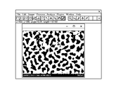
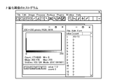
- a screen showing an example of the operation of the image analysis of the image of the pores in the uppermost layer with an electron microscope A screen showing an example of the operation of the image analysis of the image of the pores in the uppermost layer with an electron microscope
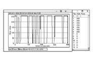
- a screen showing an example of the operation of the image analysis of the image of the pores in the uppermost layer with an electron microscope A screen showing an example of the operation of the image analysis of the image of the pores in the uppermost layer with an electron microscope
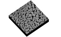
- a screen showing an example of the operation of the image analysis of the image of the pores in the uppermost layer with an electron microscope
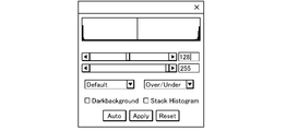
- a screen showing an example of the operation of the image analysis of the image of the pores in the uppermost layer with an electron microscope A screen showing an example of the operation of the image analysis of the image of the pores in the uppermost layer with an electron microscope
- FIG. 19B Cross-sectional view of a dielectric multilayer film in which a porous metal mask is formed to create pores.
- Flow chart of the process of forming pores on the top layer surface Sectional drawing of the process of forming a particulate metal mask in a particulate form on the outermost surface Sectional drawing of the process of forming a plurality of pores in the outermost layer
- Sectional drawing of the process of forming a porous metal mask in the form of particles on the surface of the outermost layer A conceptual diagram for explaining an example of a process of forming a particulate metal mask and a second mask on the metal mask on the uppermost layer surface according to the present invention.
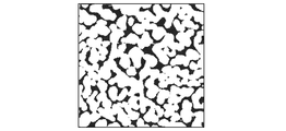
- SEM image of a sample with a particulate metal mask formed SEM image of a sample with a particulate metal mask formed SEM image of sample with vein-shaped metal mask SEM image of sample with porous metal mask
- SEM image and enlarged view showing an example of a dielectric multilayer film in which the uppermost layer is processed into a vein pattern SEM image and enlarged view showing another example of the dielectric multilayer film in which the uppermost layer is processed into a vein pattern.
- SEM image and enlarged view showing another example of the dielectric multilayer film in which the uppermost layer is processed into a vein pattern SEM image and enlarged view showing another example of the dielectric multilayer film in which the uppermost layer is processed into a vein pattern.
- the dielectric multilayer film of the present invention is a dielectric multilayer film composed of a plurality of layers on a substrate, wherein the plurality of layers are at least one low refractive index layer and at least one high refractive index layer.
- a layer, the uppermost layer farthest from the substrate is the low refractive index layer, and the high refractive index layer disposed on the substrate side of the uppermost layer is a functional layer containing a metal oxide having a photocatalytic function.
- the uppermost layer is a hydrophilic layer containing a metal oxide having a hydrophilic function, and has pores that partially expose the surface of the functional layer, and the average width of the pores.
- One feature is that the value is 5 nm or more. This feature is a technical feature common to or corresponding to the following embodiments.
- the dielectric multilayer film of the present invention can take various forms, but has one of the following features.
- the average value of the depth of the pores is in the range of 10 to 300 nm, and the average value of the width of the pores is in the range of 5 to 1000 nm.
- the maximum valley depth Sv of the pores is in the range of 10 to 300 nm, and the average width of the pores is in the range of 5 to 1000 nm.
- the average period length of the fine structure portion excluding the pores is in the range of 20 to 5000 nm.
- the area ratio of the pores on the surface of the uppermost layer when the pores are observed from the normal direction to the surface area of the uppermost layer is in the range of 1 to 70%.
- the surface of the uppermost layer is characterized in that the arithmetic mean roughness Sa is in the range of 1 to 100 nm, or the root mean square height Sq is in the range of 1 to 100 nm.
- the functional layer contains TiO 2 because it exhibits a photocatalytic function, and the uppermost layer is SiO 2 from the viewpoint of hydrophilic function. It is preferable to contain. Further, TiO 2 which is a photocatalyst material is preferable from the viewpoint of durability.
- the total layer thickness of the dielectric multilayer film is 500 nm or less, and the layer thickness of the functional layer is in the range of 10 to 200 nm, the antireflection performance is improved by thinning the functional layer, and However, the manufacturing error sensitivity of the antireflection performance becomes low, which is preferable from the viewpoint of suitability for mass production.
- the uppermost layer contains an element having an electronegativity smaller than Si, particularly, a sodium element from the viewpoint of maintaining superhydrophilicity for a long period of time.
- SiO 2 incorporating an alkali metal element has a polar electron arrangement and can attract water, which is a polar molecule, and when sodium is contained, it is generated from sodium as described above.
- NaOH which is a substance, has the property of taking in water from the external environment to become an aqueous solution, and since it takes in water under a high temperature and high humidity environment, it is preferable in that superhydrophilicity can be maintained for a long period of time.
- the film density of the uppermost layer is 98% or more because the salt water resistance can be improved.
- the uppermost layer is formed by ion-assisted vapor deposition in order to further increase the film density.
- the method for producing a dielectric multilayer film according to the present invention is a method for producing a dielectric multilayer film in which a plurality of layers are formed on a substrate, wherein at least one low refractive index layer is used as the plurality of layers.
- a step of forming certain pores is a method for producing a dielectric multilayer film in which a plurality of layers are formed on a substrate, wherein at least one low refractive index layer is used as the plurality of layers.
- the uppermost layer has an average depth value in the range of 10 to 300 nm, and an average width length value in the range of 5 to 1000 nm.
- the maximum valley depth Sv is in the range of 10 to 300 nm
- the average width length is in the range of 5 to 1000 nm in the uppermost layer
- the method for producing a dielectric multilayer film of the present invention the uppermost layer, forming the pores that partially expose the surface of the functional layer, and the average period length of the fine structure portion excluding the pores. And a step of setting the thickness within the range of 20 to 5000 nm.
- the pores that partially expose the surface of the functional layer are formed in the uppermost layer, and the pores with respect to the surface area of the uppermost layer are formed in the normal direction.
- the total area when observed from above has a range of 1 to 70% and steps.
- the uppermost layer has an arithmetic mean roughness Sa of 1 to 100 nm or a root mean square height Sq of 1 to 100 nm. And forming pores that partially expose the surface of the functional layer.
- the uppermost layer is formed with the pores that partially expose the surface of the functional layer, and the uppermost layer is formed into a vein-like structure. And a process.
- a step of forming a metal mask on the surface of the uppermost layer, and, in the uppermost layer by etching through the metal mask is a preferable manufacturing method from the viewpoint that the shape and size of the pores can be arbitrarily controlled.
- a step of forming a particle-like structure, a vein-like structure or a porous structure in the metal mask and forming the pores by dry etching may be performed. It is preferable because it can be manufactured with high precision.
- a second mask having resistance to a reactive etching process or a physical etching process is formed on the metal mask formed of Ag, for example, Ta 2 O 5
- a method of forming a film of a mixture of TiO 2 and TiO 2 (hereinafter, also referred to as H4) within a range of 0.5 to 5 nm is more preferable. At this time, it is preferable to keep the temperature of H4 at 100° C.
- the gap of silver widens after H4 film formation. That is, even if the H4 material is formed in the groove, the groove expands after the H4 film is formed, so that the groove portion can be etched.
- Having the step of forming the dielectric multilayer film by ion-assisted vapor deposition or sputtering improves the overall scratch resistance, and in particular, forms the uppermost layer into a dense film, which is resistant to salt water, scratch resistance and superhydrophilicity. It is preferable in that the property can be improved. In particular, it is preferable to apply heat of 300° C. or higher when performing the ion assisted vapor deposition.
- the dielectric multilayer film of the present invention is preferably provided in an optical member, and the optical member is a lens, an antibacterial cover member, an antifungal coating member or a mirror, and further, the optical member is a vehicle-mounted lens.
- the optical member is a lens, an antibacterial cover member, an antifungal coating member or a mirror, and further, the optical member is a vehicle-mounted lens.
- the dielectric multilayer film of the present invention (hereinafter, also simply referred to as “multilayer film”) is a dielectric multilayer film composed of a plurality of layers on a substrate, and the plurality of layers are at least one low-layer film.
- the "low refractive index layer” in the present invention means a layer having a refractive index of less than 1.7 at d-line.
- the high refractive index layer is a layer having a refractive index of 1.7 or more at d-line.
- the substrate is an optical member made of resin or glass and may have any shape.
- the transmittance at a light wavelength of 550 nm is preferably 90% or more.
- the “photocatalytic function” in the present invention refers to an organic substance decomposing effect by the photocatalyst in the present invention. This is because when TiO 2 , which has photocatalytic properties, is irradiated with ultraviolet light, active oxygen and hydroxyl radicals ( ⁇ OH radicals) are generated after electrons are emitted, and the strong oxidizing power decomposes organic substances. is there.
- ⁇ OH radicals active oxygen and hydroxyl radicals
- Whether or not it has a photocatalytic effect is evaluated, for example, in a 20° C. 80% RH environment by irradiating a sample colored with a pen with UV light at an integrated light quantity of 20 J to evaluate the color change of the pen step by step. You can judge it.
- a specific photocatalytic performance test method for self-cleaning by irradiation with ultraviolet light, for example, a methylene blue decomposition method (ISO 10678 (2010)) and a resazurin ink decomposition method (ISO 21066 (2016)) can be mentioned.
- the “hydrophilic function” in the present invention means that the water contact angle is 30 when the contact angle between the standard liquid (pure water) and the surface of the uppermost layer is measured according to the method specified in JIS R3257. What is less than or equal to ° is called “hydrophilic”, and preferably less than or equal to 15°. In particular, the case of 15° or less is defined as “superhydrophilic” in the present invention.
- Specific measurement conditions are as follows: pure water, which is the standard liquid, is dripped onto the sample at a temperature of 23° C. and a humidity of 50% RH in an amount of about 10 ⁇ L. Is measured, and the average contact angle is obtained from the average of the measured values. The time until the contact angle is measured is measured within 1 minute after dropping the standard liquid.
- the uppermost layer has a vein-like structure
- the surface of the uppermost layer is observed, for example, as shown in FIG. 2, FIG. 12, FIG. 24A to FIG. It means that the veins are formed.
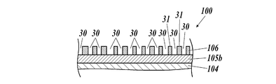
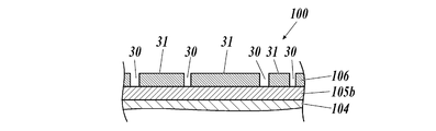
- FIG. 1 is a sectional view showing an example of the structure of the dielectric multilayer film of the present invention.
- the number of layers of the low refractive index layer and the high refractive index layer is an example, and is not limited to this.
- another thin film may be formed on the uppermost layer and between the functional layer and the uppermost layer as long as the effect of the present invention is not impaired.
- the dielectric multilayer film 100 having an antireflection function includes, for example, a high refractive index layer 103 having a refractive index higher than that of a glass substrate 101 forming a lens, and a refractive index lower than the high refractive index layer. And the low refractive index layers 102 and 104 having. Further, the uppermost layer 106 farthest from the substrate 101 is a low refractive index layer, the high refractive index layer adjacent to the uppermost layer is a functional layer 105 containing a metal oxide having a photocatalytic function as a main component, and The uppermost layer constitutes a laminate 107 having pores 30 that partially expose the surface of the functional layer and a fine structure 31 excluding the pores.
- the photocatalytic function (self-cleaning property) of the functional layer 105 can be exhibited on the surface of the dielectric multilayer film via the uppermost layer 106.
- the fine structure 31 excluding pores refers to a structural portion left by forming pores by etching the uppermost layer containing a metal oxide having a hydrophilic function with a metal mask described later.
- the dielectric multilayer film of the present invention preferably has a multilayer structure in which these high refractive index layers and low refractive index layers are alternately laminated.
- the dielectric multilayer film of the present invention has an average light reflectance of 1% or less for light incident from the normal direction in the light wavelength range of 450 to 780 nm. From the viewpoint of improving In the present invention, the dielectric multilayer film 100 is formed on the substrate 101 and constitutes an optical member.
- the light reflectance can be measured with a reflectance meter (USPM-RUIII) (manufactured by Olympus Corporation).
- the uppermost layer 106 according to the present invention is preferably a layer containing SiO 2 as a main component, and the uppermost layer preferably contains an element having an electronegativity smaller than Si, particularly sodium. It is preferable to contain the element within the range of 0.5 to 10% by mass. A more preferable content range is 1.0 to 5.0% by mass. By containing the element, it becomes possible to maintain superhydrophilicity for a long time.
- SiO 2 is the main component” means that 51% by mass or more of the total mass of the uppermost layer is composed of SiO 2 , and preferably 70% by mass or more, and particularly It is preferably 90% by mass or more.
- composition analysis of the uppermost layer according to the present invention can be performed according to a conventional method using an X-ray photoelectron spectroscopy analyzer (XPS) shown below.
- XPS X-ray photoelectron spectroscopy analyzer
- the film density of the uppermost layer is preferably 98% or more, and more preferably in the range of 98 to 100% from the viewpoint of exhibiting salt water resistance and superhydrophilicity.
- the uppermost layer is formed by ion-assisted vapor deposition from the viewpoint of further increasing the film density, and at that time, it is more preferable to apply heat of 300° or more.
- the uppermost layer of the dielectric multilayer film has a high film density, it is possible to provide a dielectric multilayer film having excellent surface salt water resistance and capable of maintaining a low water contact angle for a long period under a high temperature and high humidity environment. ..
- the “film density” means a space filling density and is defined as a value p represented by the following formula (A).
- the film density can be obtained by measuring according to the following method.
- the film density specified in the present invention is measured on the film before the etching treatment. This makes it possible to evaluate the degree of vacancy at the atomic level derived from the film formation.
- the film density of the uppermost layer is specified by comparing the theoretical value of the light reflectance calculated in (ii) with the light reflectance measured in (i).
- the light reflectance can be measured with a reflectance meter (USPM-RUIII manufactured by Olympus Corporation).
- the functional layer 105 having a photocatalytic function as a main component in a layer adjacent to the uppermost layer 106 (lower layer portion), the photocatalytic function can be effectively exhibited, and the photocatalytic effect and the photoactive effect can be achieved.
- the use of the metal oxide having the above property is a preferred embodiment because it can contribute to the maintenance of the superhydrophilicity of the uppermost layer 106 by removing the oil and surface organic matter that are the main constituents of the stain.
- the metal oxide having a photocatalytic function is preferably TiO 2 since it has a high refractive index and can reduce the light reflectance of the dielectric multilayer film.
- a low-refractive index layer, a high-refractive index layer, a functional layer and the uppermost layer 106 according to the present invention are laminated on a substrate 101 to form a laminated body 107.
- the uppermost layer according to the present invention may be formed on both sides of the substrate 101. That is, it is a preferred embodiment that the uppermost layer according to the present invention is on the side exposed to the external environment, but not on the exposed side, for example, on the inner side opposite to the exposed side, the internal environment In order to prevent the influence of the above, the uppermost layer according to the present invention may be formed.
- the optical member of the present invention can be applied to, for example, an optical member such as an antireflection member or a heat shield member.
- the uppermost layer according to the present invention is characterized by having pores of a specific shape. The details of image analysis for identifying the features of the pores will be described below.
- the image analysis method for analyzing the specific structure of the pores constituting the uppermost layer according to the present invention is not particularly limited, but as the method 1, an image analysis method 1 using an electron microscope and a method 2 are used. It is preferable to apply the image analysis method 2 using an atomic force microscope (Atomic Force Microscope AFM). Among the above methods, the image analysis method 2 using an atomic force microscope (AFM) is different from the image analysis method 1 using an electron microscope in that a sharp image can be obtained as an uneven image of the outermost layer. , A more preferable analysis method.
- AFM atomic force microscope
- image analysis of the pores forming the uppermost layer is performed at random positions in the uppermost layer.
- the result of image analysis obtained from at least a part of the position of the uppermost layer is the width of the pores defined in the present invention, the depth, the maximum valley depth, the average period length, and the arithmetic average roughness.
- the maximum valley depth Sv, the arithmetic mean roughness Sa, and the root mean square height Sq of the uppermost layer according to the present invention are the "ISO 25178" surface shape (surface roughness) which is an international standard of surface roughness. It is the value obtained in accordance with (measurement).
- the average value of the width length of the pores determined by the image analysis method is 5 nm or more in order to exert the effect of the present invention. is there.
- the depth of the pores in the uppermost layer obtained by the image analysis method is within the range of 10 to 300 nm, and the average value of the width of the pores is within the range of 5 to 1000 nm. This is a preferred embodiment from the viewpoint of sufficiently exhibiting the photocatalytic function.
- the maximum valley depth Sv of the pores of the uppermost layer obtained by the image analysis method is in the range of 10 to 300 nm, and the average value of the width of the pores is in the range of 5 to 1000 nm. Is a preferred embodiment from the viewpoint of sufficiently exhibiting the photocatalytic function.
- the maximum valley depth Sv of the pores of the uppermost layer is preferably obtained by the image analysis method 2 using AFM.
- the average period length of the fine structure excluding the pores in the uppermost layer which is obtained by the image analysis method, is in the range of 20 to 5000 nm, and by arranging the dense low-refractive material, the salt water resistance and This is a preferred embodiment from the viewpoint of further improving superhydrophilicity.
- the ratio (area ratio) of the total area when the pores are observed from the normal direction to the surface area of the uppermost layer obtained by the image analysis method is within a range of 1 to 70%,
- the maximum valley depth Sv the arithmetic mean roughness according to the ISO 25178 surface shape (surface roughness measurement), which is the international standard of surface roughness, is used as the surface roughness information from the unevenness image of the uppermost layer.
- Sa and root mean square height Sq can be calculated. If the three-dimensional arithmetic mean roughness Sa of the pores obtained by the image analysis method is in the range of 1 to 100 nm, or the root mean square height Sq is in the range of 1 to 100 nm, the photocatalytic function is sufficient. It is a preferred embodiment from the viewpoint of expression.
- the arithmetic mean roughness Sa and the root mean square height Sq of the uppermost layer are preferably obtained by the image analysis method 2 using AFM.
- the shape of the pores may be a particulate structure, a vein-like structure or a porous structure, but a vein-like structure is a preferred embodiment from the viewpoint of sufficiently exhibiting a photocatalytic function.
- Image analysis method 1 using an electron microscope As an image analysis method 1 using an electron microscope, a photograph of the pore structure of the uppermost layer is taken with a scanning electron microscope (Scanning Electron Microscope, SEM) or a transmission electron microscope (Transmission Electron Microscope; TEM). Structural analysis is performed on the photographed image using the image processing free software “ImageJ (ImageJ1.32S created by WayneRasband)”.
- the brightness value 0 is shown in black and the brightness value 255 is shown in white. If you do not put a check mark in Black Background, the brightness value 0 is shown in white and the brightness value 255 is shown in black.
- the band pass filter value be 20-100. Since this set value depends on the initial SEM image, it is preferable to set it to an optimum value.
- the threshold is set at the right end so that the above bar is 0% in the above bar (area selected in green) with the following settings.
- the Below bar (area selected in blue) adjusts the threshold until it overlaps the black area of the pore.
- the threshold changes depending on the contrast of the image, it is preferable that the threshold is set by the analyst each time instead of fixing it.
- black portions are pores (30 in FIG. 1) and white portions are microstructures (31 in FIG. 1) formed by the uppermost layer forming material excluding the pores (see FIG. 2). ..
- (A) Count the number of pixels that take the value 0 from the data in the list. In this case, 197 pixels took the value 0.
- the average value of the width of the pores is 59 nm.
- the analysis image contains information when measuring the SEM image, it is preferable to perform image analysis through steps such as excluding it so as not to affect the analysis in advance.
- the length of the straight line L is 405.
- 500 nm corresponds to the length on the screen of 167. Therefore, the physical length of the straight line L is as follows.
- the average cycle length of the peaks is 121.2 nm.
- the microstructure excluding the pores can be evaluated as having an average period length of 121 nm.
- the analysis image contains information when measuring the SEM image, it is preferable to perform image analysis through steps such as excluding it so as not to affect the analysis in advance.
- FIGS. 9A to 11 The image analysis results by electron micrographs of the uppermost layer having various pore shapes are illustrated in FIGS. 9A to 11 below.
- FIG. 9A is an electron micrograph of the uppermost porous pores
- FIG. 9B is an electron micrograph of the uppermost leaf vein-shaped pores
- FIG. 9C is another example of the uppermost porous pores. It is an electron micrograph shown.
- FIG. 10A is an electron micrograph of the uppermost granular pores
- FIG. 10B is an electron micrograph of the uppermost leaf vein-shaped pores
- FIG. 10C is another example of the uppermost porous pores. It is an electron micrograph shown.
- FIG. 11 is a screen showing an example of an operation for analyzing a photographed image of the uppermost pore by an electron microscope.
- Atomic force microscope is a kind of scanning probe microscope (SPM), and is a method for measuring nano-level unevenness structure by using atomic force between a material and a stylus.
- the AFM moves a cantilever with a sharp probe attached to the tip of a small spring plate up to a distance of several nm from the sample surface, and the interatomic force acting between the atom at the tip of the probe and the atom of the sample.
- the unevenness of the sample is measured by force.
- Atomic force microscope measures the amount of displacement fed back to the piezo scanner by performing scanning while feeding back to the piezo scanner so that the atomic force becomes constant, that is, the deflection of the cantilever becomes constant. Is a method of measuring the displacement of the Z axis, that is, the uneven structure on the surface.
- the atomic force microscope (AFM) used was Multi Mode 8 manufactured by BRUKER, and the probe was Model RTESPA-150, which is also a silicon probe manufactured by BRUKER.
- AFM atomic force microscope
- binarization is performed by using the midpoint between the surface and bottom of the pore as a threshold. Specifically, the area higher than the height of the midpoint (threshold) is displayed in white, and the area lower than the height of the midpoint is displayed in black (see FIG. 14).
- the surface referred to in the present invention is defined as the height at which the number of data on the surface side is the largest, and the bottom is defined as the height of the deepest data.
- the image created in this way using the free software ImageJ, which is the image analysis software described above, similarly, the average value of the pore width length, the average period length of the fine structure portion of the pores, Measure the ratio of total area.
- the profile length of 5 ⁇ m is divided by the number of peaks to obtain the average period of the peaks and grooves.
- a value of 128 or more which is a half value, is determined to be a wall region, and a value smaller than 128 is determined to be a groove region. Then, the total number of pieces of data in the wall area is added up to calculate the total physical length of the wall area.
- the average groove length can also be calculated by the same procedure as above, and in the above case, the average groove length was 133 nm.
- the half value of 128 or more is defined as the wall area, and the value less than 128 is defined as the groove area.
- the ratio of the number of data in the groove region to the total data is calculated, and this is obtained as the area ratio of the pores.
- the maximum valley depth Sv is the maximum value (absolute value) of the valley depth Rv from the average value of the surface of the contour curve at the reference length, and this Rv is expanded and displayed on the surface.
- the arithmetic average roughness Sa is expressed as an average value of absolute values of height differences at respective points with respect to the average surface of the surface.
- the root mean square height Sq is a parameter displayed as the standard deviation of the distance from the average surface of the surface.
- 25 and 26 show an example of measurement data of the maximum valley depth Sv, the arithmetic mean roughness Sa, and the root mean square height Sq obtained by the AFM.
- FIG. 25 shows data of the dielectric multilayer film 51 produced in Example 2 described later
- FIG. 26 shows data of the dielectric multilayer film 52 similarly.
- the dielectric multilayer film having an antireflection function preferably has a high refractive index layer having a refractive index higher than that of the substrate and a low refractive index layer having a refractive index lower than that of the high refractive index layer. It is preferable to have a laminated body in which these high refractive index layers and low refractive index layers are alternately laminated.
- the number of layers is not particularly limited, but it is preferably 12 or less from the viewpoint of maintaining high productivity and obtaining a desired antireflection effect. That is, although the number of layers in the laminate depends on the required optical performance, a reflectance of the entire visible region can be reduced by using a layered structure of about 3 to 8 layers, and the upper limit of the number of layers can be reduced. It is preferable that the number of layers is 12 or less, because peeling between layers can be prevented even when the stress applied to the laminated structure becomes large.
- the material used for forming the laminate (high refractive index layer, low refractive index layer) according to the present invention is preferably, for example, Ti, Ta, Nb, Zr, Ce, La, Al, Si, and Hf. Are suitable, or an oxide compound or a combination thereof and MgF 2 are suitable. Also, by stacking a plurality of layers of different dielectric materials, it is possible to add a function of reducing the reflectance in the entire visible range.
- the low refractive index layer is made of a material having a refractive index of less than 1.7, and in the present invention, it is preferably a layer containing SiO 2 as a main component. However, it is also preferable to contain other metal oxides, and it is also preferable to use a mixture of SiO 2 and part of Al 2 O 3 or MgF 2 from the viewpoint of light reflectance.
- the high refractive index layer is made of a material having a refractive index of 1.7 or more.
- a material having a refractive index of 1.7 or more For example, a mixture of a Ta oxide and a Ti oxide, a Ti oxide, a Ta oxide, and a La oxide are mixed. It is preferable that it is a mixture of a substance and an oxide of Ti.
- the metal oxide used in the high refractive index layer preferably has a refractive index of 1.9 or more. In the present invention, Ta 2 O 5 or TiO 2 is preferable, and Ta 2 O 5 is more preferable.
- the total thickness of the laminate composed of the high refractive index layer and the low refractive index layer is not particularly limited, but is 500 nm or less from the viewpoint of antireflection performance. Is preferable, and more preferably within the range of 50 to 500 nm. When the thickness is 50 nm or more, the antireflection optical characteristics can be exhibited, and when the thickness is 500 nm or less, the error sensitivity is reduced and the yield rate of the spectral characteristics of the lens can be improved.
- the method for producing a dielectric multilayer film according to the present invention is a method for producing a dielectric multilayer film in which a plurality of layers are formed on a substrate, wherein at least one low refractive index layer is used as the plurality of layers.
- the average depth of the pores is in the range of 10 to 300 nm, and the average width of the pores is 5 to.
- the uppermost layer has pores having a maximum valley depth Sv within a range of 10 to 300 nm and an average width length of 5 to 1000 nm. Within the range, and forming the pores that partially expose the surface of the functional layer.
- the average period length of the fine structure portion excluding the pores is in the range of 20 to 5000 nm, and the fine layer that partially exposes the surface of the functional layer is used. And a step of forming a hole.
- the total area of the pores with respect to the surface area of the uppermost layer when observed from the normal direction is within a range of 1 to 70%, And a step of forming the pores that partially expose the surface.
- the uppermost layer has an arithmetic mean roughness Sa of 1 to 100 nm or a root mean square height Sq of 1 to 100 nm. And forming pores that partially expose the surface of the functional layer.
- the shape of the pores is a vein-like structure, and a step of forming the pores that partially expose the surface of the functional layer, It is a feature.
- a vapor deposition system includes a vacuum vapor deposition method, an ion beam vapor deposition method, an ion plating method, and a sputtering system.
- a sputtering method, an ion beam sputtering method, a magnetron sputtering method and the like are known, as a film forming method for forming the dielectric multilayer film of the present invention, an ion assisted vapor deposition method (hereinafter, also referred to as “IAD method” in the present invention) is used.
- IAD method ion assisted vapor deposition method
- the uppermost layer is a high density film formed by using an ion assisted vapor deposition method.
- Each of the other layers of the dielectric multilayer film is formed by a vapor deposition method, and one of the layers is preferably formed by the IAD method, and all layers are formed by the IAD method. Is more preferable.
- the scratch resistance of the entire dielectric multilayer film can be further improved.
- the film density can be increased by forming the uppermost layer 106 among them by the IAD method, the sputtering method, or the like.
- the film density of the uppermost layer 106 is preferably 98% or more.
- the film density means the space filling density as described above.
- the IAD method is a method in which high kinetic energy of ions is applied during film formation to form a dense film to enhance the adhesion force of the film.
- a method using an ion beam is an ionized gas irradiated from an ion source. This is a method of accelerating the deposition material by molecules and forming a film on the substrate surface.
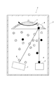
- FIG. 18 is a schematic diagram showing an example of a vacuum vapor deposition apparatus using the IAD method.
- a vacuum vapor deposition apparatus 1 using the IAD method (hereinafter, also referred to as an IAD vapor deposition apparatus in the present invention) includes a dome 3 inside a chamber 2, and a substrate 4 is arranged along the dome 3.
- the vapor deposition source 5 is equipped with an electron gun or a resistance heating device that evaporates the vapor deposition substance, and the vapor deposition substance 6 is scattered from the vapor deposition source 5 toward the substrate 4, and is condensed and solidified on the substrate 4.
- the ion beam 8 is radiated from the IAD ion source 7 toward the substrate, and the high kinetic energy of the ions is applied during the film formation to form a dense film or increase the adhesion of the film.
- the substrate 4 used in the present invention may be a resin such as glass or a polycarbonate resin or a cycloolefin resin, and is preferably an on-vehicle lens.
- a plurality of vapor deposition sources 5 are arranged on the bottom of the chamber 2.
- one vapor deposition source is shown as the vapor deposition source 5, but the number of vapor deposition sources 5 to be arranged may be plural.
- the deposition material 6 of the deposition source 5 By depositing the deposition material 6 of the deposition source 5 by an electron gun or resistance heating to generate the deposition material 6 and scattering and depositing the deposition material on the substrate 4 (for example, lens) installed in the chamber 2.
- a layer made of a film forming material for example, SiO 2 , MgF 2 or Al 2 O 3 which is a low refractive index material, Ta 2 O 5 or TiO 2 which is a high refractive index material
- the uppermost layer 106 containing SiO 2 When forming the uppermost layer 106 containing SiO 2 according to the present invention, it is preferable to dispose a SiO 2 target on the vapor deposition source 5 and form a layer containing SiO 2 as a main component. In order to further improve the hydrophilic function, it is preferable to mix an element having an electronegativity smaller than Si with the SiO 2 , and examples of the element having an electronegativity smaller than Si include a lithium element, a sodium element, and magnesium. Examples include elements, potassium elements, calcium elements, and the like.
- a sodium-containing SiO 2 target When elemental sodium is added, a sodium-containing SiO 2 target can be prepared, and this target can be placed in a vapor deposition source for direct vapor deposition.
- the SiO 2 target and the sodium target may be separately arranged, and SiO 2 and sodium may be vapor-deposited by co-evaporation.
- Na 2 O sodium
- Li 2 O lithium
- MgO magnesium
- K 2 O potassium
- CaO calcium
- the chamber 2 is provided with a vacuum exhaust system (not shown), so that the chamber 2 is evacuated.
- the degree of reduced pressure in the chamber is usually in the range of 1 ⁇ 10 ⁇ 4 to 1 ⁇ 10 ⁇ 1 Pa, preferably 1 ⁇ 10 ⁇ 3 to 1 ⁇ 10 ⁇ 2 Pa.
- the dome 3 holds at least one holder (not shown) that holds the substrate 4, and is also called a vapor deposition umbrella.
- the dome 3 has an arcuate cross section, and has a rotationally symmetric shape in which the dome 3 passes through the center of a chord connecting both ends of the arc and rotates about an axis perpendicular to the chord as a rotational symmetry axis.
- the dome 3 rotates about the axis at a constant speed, for example, the substrate 4 held by the dome 3 via the holder revolves around the axis at a constant speed.
- This dome 3 can hold a plurality of holders arranged side by side in the rotation radius direction (revolution radius direction) and the rotation direction (revolution direction). As a result, it becomes possible to simultaneously form a film on the plurality of substrates 4 held by the plurality of holders, and it is possible to improve the manufacturing efficiency of the element.
- the IAD ion source 7 is a device that introduces argon gas or oxygen gas into the main body to ionize them, and irradiates the ionized gas molecules (ion beam 8) toward the substrate 4.
- the argon gas and the oxygen gas are provided in the vicinity of the IAD ion source 7 in order to prevent the phenomenon that the whole substrate is positively charged (so-called charge-up) due to the accumulation of positive ions irradiated from the ion gun on the substrate.
- a neutralizer that emits a negative charge may be provided. This serves to electrically neutralize the positive charges accumulated on the substrate.
- the Kaufman type (filament), hollow cathode type, RF type, bucket type, duoplasmatron type, etc. can be applied as the ion source.
- the IAD ion source 7 By irradiating the substrate 4 with the above-mentioned gas molecules from the IAD ion source 7, for example, molecules of a film-forming material that evaporates from a plurality of evaporation sources can be pressed against the substrate 4, and a film having high adhesion and denseness can be formed on the substrate. 4 can be deposited.
- the IAD ion source 7 is installed so as to face the substrate 4 at the bottom of the chamber 2, but may be installed at a position offset from the facing axis.
- an ion beam with an accelerating voltage of 100 to 2000 V an ion beam with a current density of 1 to 120 ⁇ A/cm 2 , or a current density of 1 to 120 ⁇ A/cm with an accelerating voltage of 500 to 1500 V.
- An ion beam within the range of 2 can be used.
- the irradiation time of the ion beam can be set within a range of, for example, 1 to 800 seconds, and the number of particles irradiated by the ion beam can be set at, for example, 1 ⁇ 10 13 to 5 ⁇ 10 17 particles/cm 2. Can be within the range of.
- the ion beam used in the film formation step can be an oxygen ion beam, an argon ion beam, or an oxygen/argon mixed gas ion beam.
- the oxygen introduction amount is within a range of 30 to 60 sccm and the argon introduction amount is within a range of 0 to 10 sccm.
- SCCM here is an abbreviation for standard cc/min, and is a unit showing how many cc flows per minute at 1 atmospheric pressure (atmospheric pressure 10 13 hPa) and 0°C.
- the monitor system (not shown) is a system that monitors the wavelength characteristics of the layer formed on the substrate 4 by monitoring the layer evaporated from each vapor deposition source 5 and attached to itself during vacuum film formation. .. With this monitor system, the optical characteristics of the layer formed on the substrate 4 (for example, spectral transmittance, light reflectance, optical layer thickness, etc.) can be grasped.
- the monitor system also includes a crystal layer thickness monitor, and can monitor the physical layer thickness of the layer formed on the substrate 4. This monitor system also functions as a control unit that controls ON/OFF switching of the plurality of evaporation sources 5 and ON/OFF switching of the IAD ion source 7 according to the monitoring result of the layer.
- bipolar sputtering, magnetron sputtering, dual magnetron sputtering (DMS) using an intermediate frequency region, ion beam sputtering, ECR sputtering, etc. may be used alone or in combination of two or more. it can.
- the target application method is appropriately selected according to the target type, and either DC (direct current) sputtering or RF (high frequency) sputtering may be used.
- the sputtering method may be multi-source simultaneous sputtering using multiple sputtering targets.
- the method for producing these sputtering targets and the method for producing a thin film using these sputtering targets for example, JP-A-2000-160331, JP-A-2004-068109, and JP-A-2013-047361. The description such as can be appropriately referred to.
- SiO 2 is used as the main component in the uppermost layer 106
- a layer containing TiO 2 as a photocatalyst layer having a self-cleaning function, as a layer adjacent to the uppermost layer 106.
- the self-cleaning function of TiO 2 means the organic substance decomposition effect by the photocatalyst, as described above. This is because when TiO 2 is irradiated with ultraviolet light, ⁇ OH radicals are generated after electrons are emitted, and organic substances are decomposed by the strong oxidizing power of the ⁇ OH radicals.
- the TiO 2 -containing layer By adding the TiO 2 -containing layer to the dielectric multilayer film of the present invention, it is possible to prevent the organic matter and the like attached to the optical member from being contaminated and contaminating the optical system.
- the upper SiO 2 -containing layer has the pores according to the present invention, because the OH radicals can easily move and the antifouling property of the optical member surface can be improved.
- the dielectric multilayer film 100 of the present invention preferably satisfies the following conditional expressions (1) and (2).
- Conditional expression (1) 10 nm ⁇ TL ⁇ 300 nm
- Conditional expression (2) 10 nm ⁇ Tcat ⁇ 600 nm
- TL represents the layer thickness of the uppermost layer 106
- Tcat represents the layer thickness of the functional layer 105 adjacent to the uppermost layer 106.
- conditional expression (1) when the value of TL is equal to or less than the upper limit value, the photocatalytic effect is easily exhibited by exchanging active oxygen excited by UV light through the plurality of pores 30 provided in the uppermost layer 106.
- conditional expression (1) when the value of TL is equal to or more than the lower limit value, the hydrophilic function of the uppermost layer 106 can be easily maintained, and a strong uppermost film can be formed, so that sufficient salt water resistance can be secured.
- the uppermost layer thickness of the dielectric multilayer film 100 further satisfies the following conditional expression (1b).
- Conditional expression (1b) 60 nm ⁇ TL ⁇ 250 nm
- the layer thickness of the functional layer 105 can be secured, and a sufficient photocatalytic effect can be expected.
- the upper limit of the value of Tcat in conditional expression (2) is used. The following is desirable.
- the layer thickness of the functional layer 105 further preferably satisfies the following conditional expression (2b).
- the functional layer 105 adjacent to the uppermost layer 106 is formed of an oxide containing Ti as a main component (for example, TiO 2 ).
- Ti oxides such as TiO 2 have a very high photocatalytic effect.
- anatase-type TiO 2 is desirable as a material for the functional layer 105 because it has a high photocatalytic effect.
- the uppermost layer 106 is preferably formed of, for example, SiO 2 as a main component.
- the uppermost layer 106 preferably contains SiO 2 in an amount of 90 mass% or more.
- UV light is difficult to enter at night or outdoors, and the hydrophilic function is deteriorated by the oxide containing Ti as a main component, but even in such a case, the hydrophilic function can be exhibited by forming the uppermost layer 106 from SiO 2 . Saltwater tolerance is also increased.
- the hydrophilicity is preferably such that the contact angle when 10 ⁇ L of water droplets is dropped on the dielectric multilayer film 100 is 30° or less, and superhydrophilicity of 15° or less.
- the uppermost layer 106 may be formed of a mixture of SiO 2 and Al 2 O 3 (however, the composition ratio of SiO 2 is 90 mass% or more). As a result, the hydrophilic effect can be exhibited at night or outdoors, and the scratch resistance can be further enhanced by using a mixture of SiO 2 and Al 2 O 3 . When a mixture of SiO 2 and Al 2 O 3 is used for the uppermost layer 106, heat resistance at 200° C. or higher for 2 hours after film formation can improve scratch resistance.
- the dielectric multilayer film 100 preferably satisfies the following conditional expression (3).
- NL represents the refractive index of the material of the low refractive index layer at the d line.
- the dielectric multilayer film 100 having desired optical characteristics can be obtained.
- the d-line refers to light having a wavelength of 587.56 nm.
- SiO 2 having a refractive index of 1.48 at the d-line or MgF 2 having a refractive index of 1.385 at the d-line can be used.
- the dielectric multilayer film 100 preferably satisfies the following conditional expression (4).
- Ns represents the refractive index of the base material at the d-line.
- the dielectric multilayer film of the present invention By satisfying the condition defined by the conditional expression (4) as the refractive index of the substrate at the d-line, it is possible to improve the optical performance of the dielectric multilayer film 100 while having a compact structure. ..
- the dielectric multilayer film of the present invention By forming the dielectric multilayer film of the present invention on the glass substrate GL that satisfies the conditional expression (4), it can be used for a lens exposed to the outside and the like, and has excellent environmental resistance and optical performance. Can be compatible.
- a functional layer containing a metal oxide having a photocatalytic function as a main component is arranged, and the uppermost layer has a plurality of pores that partially expose the surface of the functional layer. Is preferable.
- 19A to 19D are schematic diagrams showing the functional layer according to the present invention and the uppermost layer having pores.
- FIG. 19A is a diagram schematically showing a cross section of the dielectric multilayer film 100 formed by forming a particulate metal mask
- FIG. 19B is a dielectric multilayer film formed by forming a vein-shaped metal mask
- 19C is a diagram schematically showing a cross section of FIG. 19C
- FIG. 19C is a SEM image of the surface of the uppermost layer of FIG. 19B
- FIG. 19D is a dielectric multilayer film in which pores 30 are formed by forming a porous metal mask. It is a figure which shows the cross section of FIG.
- the uppermost layer 106 has a plurality of pores 30 for allowing the adjacent functional layer 105 serving as a high refractive index layer to exhibit a photocatalytic function.
- the pores 30 are formed by dry etching.
- the ratio of the total area of the cross-sections of the plurality of pores 30 to the surface area of the uppermost layer 106 (the total area of the pores 30 when the uppermost layer 106 is viewed from the normal direction) hereinafter, the pore density or the film falling rate.
- the film drop-out rate is preferably in the range of 5 to 30%.
- the cross section of the pore 30 has a random shape.
- FIG. 21A to FIG. 21E, FIG. 22A to FIG. 22E, FIG. 23A to FIG. 23D, and FIG. 24A to FIG. 24C the manufacturing method for forming pores in the dielectric multilayer film 100 and the uppermost layer explain.
- FIG. 20 is a flowchart of a process of forming pores on the surface of the uppermost layer according to the present invention.
- 21A to 21C are conceptual diagrams for explaining a process of forming a particulate metal mask and forming pores on the surface of the uppermost layer according to the present invention.
- 22A to 22C are conceptual diagrams illustrating an example of a process of forming a particulate metal mask and a second mask on the metal mask to form pores on the surface of the uppermost layer according to the present invention.
- 23A to 23D are SEM images of the surface of the uppermost layer according to the present invention in which each metal mask is formed.
- 24A to 24C are SEM images and enlarged views with different enlargement ratios when the uppermost surface according to the present invention is processed into a vein pattern.
- a low refractive index layer and a high refractive index layer as a multilayer film are alternately laminated on a glass base material (glass substrate) (multilayer film forming step: step S11).
- steps S11 layers other than the uppermost layer 106 and the functional layer 105 of the multilayer film are formed. That is, the low refractive index layer adjacent to the lower side of the functional layer 105 is formed.
- the multilayer film is formed by various vapor deposition methods, ion assisted vapor deposition methods (IAD methods), sputtering methods, or the like.
- IAD methods ion assisted vapor deposition methods
- sputtering methods or the like.
- the formation of the multilayer film in step S11 may be omitted depending on the configuration of the dielectric multilayer film 100.
- step 12 the functional layer 105 is formed, and subsequently, in step 13, the uppermost layer 106 is formed.
- a forming method it is preferable to form a film by an IAD method or a sputtering method, and it is more preferable to use the IAD method.
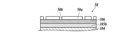
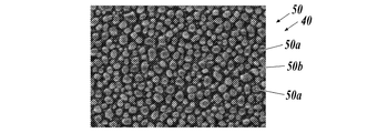
- the metal mask 50 is formed on the surface of the uppermost layer 106 (mask forming step: step S14). As shown in FIGS. 21A and 23A, the metal mask 50 is formed in a particle shape on the surface of the uppermost layer 106. Thereby, the nano-sized metal mask 50 can be formed on the uppermost layer 106.
- the metal mask 50 may be formed into a vein as shown in FIGS. 21D and 23C. Further, as shown in FIGS. 21E and 23D, the metal mask 50 may be formed in a porous shape.
- the metal mask 50 is composed of a metal portion 50a and an exposed portion 50b.
- the layer thickness of the metal mask 50 is in the range of 1 to 30 nm. Although it depends on the film forming conditions, when the metal mask 50 is formed to have a layer thickness of 2 nm by using, for example, a vapor deposition method, the metal mask 50 is likely to be in the form of particles (FIGS. 23A and 23C). Further, for example, when the metal mask 50 is formed to have a layer thickness of 12 to 15 nm by using the vapor deposition method, the metal mask 50 tends to have a vein pattern (FIG. 23C).
- the metal mask 50 tends to have a porous shape (FIG. 23D).
- the metal mask 50 By depositing the metal to a thickness within the above range, it is possible to easily form the optimum metal mask 50 having a particle shape, a leaf vein shape, or a porous shape.
- FIGS. 22A to 22E are different from FIGS. 21A to 21E described above in that they protect the upper portion of the particulate metal mask 50 from damage due to dry etching or the like when forming pores in the metal mask. It is a conceptual diagram explaining an example of the process of forming the 2nd mask 51 which has a function, and forming a pore in the uppermost layer surface which concerns on this invention.
- a second mask 51 having resistance to the reactive etching process or the physical etching process is formed on the metal mask 50, for example, Ta.
- a form of forming a film of a mixture of 2 O 5 and TiO 2 (hereinafter, also referred to as H4) within a range of 0.5 to 5 nm is also one of the preferable forms as the metal mask applied to the present invention.
- H4 a form of forming a film of a mixture of 2 O 5 and TiO 2
- the metal mask 50 is formed of, for example, Ag or Al, and is particularly silver, and the film formation temperature is controlled within the range of 20° C. to 400° C. and the thickness within the range of 1 to 100 nm. This is preferable from the viewpoint of controlling the shape of the pores.
- step S15 a plurality of pores 30 are formed in the uppermost layer 106 (pore forming step: step S15).
- etching dry etching using an etching device (not shown) or a device in which an etching gas is introduced into an IAD vapor deposition device is used.
- the film forming apparatus used for forming the above-described multilayer film or forming the metal mask 50 may be used.
- the pore forming step a plurality of pores are formed by using a material that reacts with the material of the uppermost layer 106, specifically, SiO 2 . In this case, the SiO 2 of the uppermost layer 106 can be removed without damaging the metal mask 50.
- the etching gas for example, CHF 3 , CF 4 , COF 2, SF 6 or the like is used.
- a plurality of pores 30 exposing the surface of the functional layer 105 are formed in the uppermost layer 106. That is, the uppermost layer 106 corresponding to the exposed portion 50b of the metal mask 50 is etched to form the pores 30 and the fine structure 31 of SiO 2 which is the uppermost layer forming material, and the surface of the functional layer 105 is partially exposed. It becomes a state.
- the metal mask 50 is removed (mask removing step: step S16).
- the metal mask 50 and the second mask 51 are removed.
- the metal mask 50 and the second mask 51 are removed by wet etching using acetic acid or the like.
- the metal mask 50 and the second mask 51 may be removed by dry etching using Ar or O 2 as an etching gas, for example.
- the dielectric multilayer film 100 having the plurality of pores 30 in the uppermost layer 106 can be obtained by the above steps.
- a plurality of pores 30 for exhibiting a photocatalytic function are formed in the functional layer 105, thereby achieving both superhydrophilicity and a photocatalytic function. Can be made. Further, the pores 30 have a size that allows the functional layer 105 to exhibit a photocatalytic function, are not visually recognized by the user, and have resistance to salt water.
- the functional layer 105 exhibits a photocatalytic function, since it is a high refractive index layer, in order to maintain the antireflection property of the dielectric multilayer film 100, the uppermost layer 106, which is a low refractive index layer, is provided on the functional layer 105. Need to be provided. Therefore, conventionally, when the density of the uppermost layer 106 is high, there is a problem that the photocatalytic function of the functional layer 105 is not exhibited. On the other hand, when the film density of the uppermost layer 106 is lowered, there is a problem that the saltwater resistance of the uppermost layer 106 is lowered.
- the photocatalytic function of the functional layer 105 is maintained while maintaining antireflection properties, superhydrophilicity, and saltwater resistance. Can be expressed.
- the dielectric multilayer film 100 is a dielectric multilayer film having low light reflectance, hydrophilicity, and photocatalytic property, and is also excellent in characteristics such as salt water resistance or scratch resistance.
- the optical member is a lens, an antibacterial cover member, an antifungal coating member or a mirror, for example, an in-vehicle lens or a communication lens.
- Suitable for lenses, antibacterial lenses for endoscopes, antibacterial cover members for PCs and smartphones, eyeglasses, pottery for toilets and tableware, antifungal coatings for baths and sinks, or building materials (window glass), among others, in-vehicle lenses Is suitable as
- Example 1 Hereinafter, specific examples of the dielectric multilayer film 100 according to the present embodiment will be described.
- a film deposition apparatus (BES-1300) (manufactured by Syncron Co., Ltd.) was used to manufacture the following dielectric multilayer film.
- Dielectric Multilayer Film 1 A low refractive index layer using SiO 2 (manufactured by Merck) on a glass substrate TAFD5G (manufactured by HOYA CORPORATION: refractive index 1.835), OA600 (materials manufactured by Canon Optron: Ta 2 O 5 , TiO 2 ) , the high refractive index layer using the mixture) of Ti 2 O 5 until the layer numbers 1 to 3 in Table I, and laminated at a predetermined thickness using the IAD process under the following conditions.
- Film forming conditions > (Conditions in chamber) Heating temperature 370°C Starting vacuum degree 1.33 ⁇ 10 -3 Pa (Evaporation source of film forming material) Electron gun ⁇ Formation of low refractive index layer, high refractive index layer, functional layer and uppermost layer> Film forming material for low refractive index layer: SiO 2 (trade name SiO 2 manufactured by Canon Optron) The above substrate is installed in an IAD vacuum vapor deposition apparatus, the first evaporation source is charged with the above film forming material, and the film is evaporated at a film forming rate of 3 ⁇ /sec. A 5 nm low refractive index layer (layer 1 and layer 3) was formed.
- IAD For the IAD method, an accelerating voltage of 1200 V, an accelerating current of 1000 mA, and a neutralizing current of 1500 mA were used, and a device of RF ion source "OIS One" manufactured by Optolan Corporation was used. IAD was introduced under the conditions of O 2 50 sccm, Ar gas 10 sccm, and neutral gas Ar 10 sccm.
- Film forming material for high refractive index layer Ta 2 O 5 (trade name OA-600 manufactured by Canon Optron) The film forming material was loaded in the second evaporation source and vapor deposition was carried out at a film forming rate of 3 ⁇ /sec to form a high refractive index layer (layer 2) having a thickness of 33.2 nm on the low refractive index layer.
- the formation of the high refractive index layer was similarly performed by the IAD method and 370° C. heating conditions.
- Film forming material for the functional layer TiO 2 (trade name TOP (Ti 3 O 5 ) manufactured by Fuji Titanium Industry Co., Ltd.)
- the above base material is installed in a vacuum vapor deposition apparatus, the third evaporation source is charged with the above film forming material, and vapor deposition is performed at a film forming rate of 3 ⁇ /sec, and a functional layer having a thickness of 105 nm is formed on the low refractive index layer. (Layer 4) was formed.
- the formation of the functional layer was similarly performed under the IAD method and 370° C. heating conditions.
- the uppermost layer film-forming material SiO 2 and Na 2 O (manufactured by Toshima Seisakusho Co., Ltd., trade name SiO 2 —Na 2 O) were mixed at a mass ratio of 95:5 to prepare particles.
- the above base material is installed in a vacuum vapor deposition apparatus, the fourth evaporation source is charged with the film forming material, and vapor deposition is carried out at a film forming rate of 3 ⁇ /sec, and the uppermost layer (layer having a thickness of 112 nm) is formed on the functional layer. 5) was formed.
- the formation of the functional layer was similarly performed under the IAD method and 370° C. heating conditions.
- the layer thickness (layer thickness) of each layer was measured by the following method.
- each layer is formed on the TiO 2 and SiO 2 film under the above-mentioned film forming conditions, the spectral reflectance is measured, and the refractive index and the layer thickness of the layer are calculated from the change amount. To do.
- composition analysis of the uppermost layer was measured using the following X-ray photoelectron spectroscopy analyzer (XPS).
- XPS composition analysis ⁇ Device name: X-ray photoelectron spectroscopy analyzer (XPS) ⁇ Device type: Quantera SXM ⁇ Device manufacturer: ULVAC-PHI ⁇ Measurement condition: X-ray source: Monochromatic AlK ⁇ ray 25W-15kV ⁇ Degree of vacuum: 5.0 ⁇ 10 -8 Pa Depth analysis is performed by argon ion etching. For data processing, MultiPak manufactured by ULVAC-PHI, Inc. was used.
- the light reflectance was measured with an ultraviolet-visible near-infrared spectrophotometer V-670 manufactured by JASCO Corporation at an optical wavelength of 587.56 nm (d line).
- the refractive index shown in Table I is calculated by forming each layer of the multilayer film as a single layer and measuring the light reflectance at the d-line using a spectrophotometer U-4100 manufactured by Hitachi High-Technologies Corporation. ..
- the thin film calculation software (Essential Macleod) (manufactured by Sigma Optical Co., Ltd.) was used to specify the refractive index of the layer obtained by adjusting the refractive index so as to fit the actually measured light reflectance data.
- ⁇ Formation of pores in top layer> After forming the uppermost layer (layer 5), Ag is used as a mask material, a vapor deposition method is used as a mask film formation, a metal mask thickness is 12 nm, and a mask shape is used according to the pore forming method shown in FIGS. 20 and 21A to 21E.
- a film forming apparatus (BES-1300) (manufactured by Syncron Co., Ltd.) was used for Ag film formation under the following conditions. By changing the layer thickness at the time of film formation, leaf vein-shaped, porous and particle-shaped Ag masks were formed.
- Dielectric Multilayer Films 2 to 16 were prepared.
- the film forming temperature, thickness and etching conditions of the metal mask are changed to change the width and depth of the pores, the average period length of the fine structure excluding the pores, and the pore area ratio. Controlled. Further, the vapor deposition conditions of the IAD method were controlled, and each of the functional layer layer thickness, the uppermost layer thickness, the total layer thickness and the uppermost layer sodium content was changed as described in Table II, and the same procedure was performed. Dielectric multilayer films 2 to 16 were prepared.
- the depth of the pores controls the layer thickness of the uppermost layer, and when the functional layer layer thickness is changed, the layer thicknesses of layers 1 to 3 are appropriately changed to control the total layer thickness.
- the content of SiO 2 was set to 40 mass %, and the balance was co-evaporated with Al 2 O 3 .
- Dielectric Multilayer films 17 to 19 In the production of the dielectric multilayer film 1, the metal mask thickness was set to 10 nm, a porous mask was produced, and the porous pores shown in FIG. 23D were formed in the same manner. Dielectric multilayer films 17 to 19 having width, depth, average period length of fine structure excluding pores, and pore area ratio were prepared.
- the content of TiO 2 in the functional layer was changed, but the remaining part was co-evaporated with WO 3 .
- the content of SiO 2 in the uppermost layer was 70% by mass, and Al 2 O 3 was co-evaporated as the balance.
- Dielectric Multilayer films 20-23 In the production of the dielectric multilayer film 1, the metal mask thickness was set to 2 nm and a particle-shaped mask was produced in the same manner except that the particulate pores shown in FIG. 23A were formed. Dielectric multilayer films 20 to 23 having width, depth, average period length of fine structure excluding pores, and pore area ratio were prepared.
- ⁇ Measurement of each parameter in the top layer>> According to the image analysis method 1 using the electron microscope described above, a photograph of the pore structure of the uppermost layer was taken with a scanning electron microscope (Scanning Electron Microscope, SEM), and the image photographed was subjected to image processing according to the method described above. Using the free software “ImageJ (ImageJ1.32S created by WayneRasband)”, the pore width length (nm), the pore depth (nm), the fine structure period length (nm), the pore area ratio (%) and the fine area ratio (%). The pore shape was measured and the results obtained are shown in Table II. ⁇ Evaluation of dielectric multilayer film>> (1) Measurement of film density of uppermost layer The film density of the uppermost layer of each dielectric multilayer film was measured by the following method.
- ⁇ When the film density is 98% or more, it is ⁇ , when it is 90 to 97%, it is ⁇ , and when it is less than 90%, it is x.
- ⁇ The degree of color change after UV irradiation is large, the color of the pen is completely erased, and it has an excellent photocatalytic effect.
- ⁇ After UV irradiation, the color of the pen almost disappears and a good photocatalytic effect is obtained.
- ⁇ Measurement of water contact angle> The contact angle between the standard liquid (pure water) and the surface of the uppermost layer was measured according to the method defined in JIS R3257. About 10 ⁇ L of pure water, which is the standard liquid, was dropped onto the sample at a temperature of 23° C. and a humidity of 50% RH, and five points on the sample were measured by a G-1 device manufactured by Elma Co., The average contact angle was obtained from the average of the measured values. The time until the contact angle is measured is measured within 1 minute after dropping the standard liquid.
- ⁇ Change in light reflectance is less than 0.5%.
- ⁇ Change in light reflectance is 0.5% or more and less than 2.0%.
- x Change in light reflectance is 2.0% or more.
- ⁇ Change in light reflectance is less than 0.5%.
- ⁇ Change in light reflectance is 0.5% or more and less than 2.0%.
- x Change in light reflectance is 2.0% or more.
- Table III shows the configuration of the dielectric multilayer film and the above evaluation results. From the results shown in Table III, the dielectric multilayer films 1 to 23 of the present invention have hydrophilicity and photocatalytic properties as compared with the dielectric multilayer film 24 of the comparative example, and also have excellent properties such as salt water resistance and scratch resistance. It is clear that it is a dielectric multilayer film.
- the pores were not clogged even after the high temperature and high humidity test, and the shape and size of the pores for efficiently extracting the photocatalyst were clarified.
- the shape of the pores are veins, the width of the pores, the depth, the average period length of the microstructure excluding the pores, and the value of the pore area ratio, the preferred range of the present invention.
- Example 2 ⁇ Preparation of dielectric multilayer film>> [Production of Dielectric Multilayer Film 51]
- a high refractive index layer using a mixture of Ti 2 O 5 was laminated up to the layer numbers 1 to 3 in Table IV at a predetermined layer thickness by the IAD method under the following conditions.
- Film forming conditions (Conditions in chamber) Heating temperature 370°C Starting vacuum degree 1.33 ⁇ 10 -3 Pa (Evaporation source of film forming material) Electron gun ⁇ Formation of low refractive index layer, high refractive index layer, functional layer and uppermost layer> Film forming material for low refractive index layer: SiO 2 (trade name SiO 2 manufactured by Canon Optron) The above substrate is installed in an IAD vacuum vapor deposition apparatus, the first evaporation source is charged with the above film forming material, and the film is evaporated at a film forming rate of 3 ⁇ /sec. A 3 nm low refractive index layer (Layer 1 and Layer 3) was formed.
- IAD For the IAD method, an accelerating voltage of 1200 V, an accelerating current of 1000 mA, and a neutralizing current of 1500 mA were used, and a device of RF ion source "OIS One" manufactured by Optolan Corporation was used. IAD was introduced under the conditions of O 2 50 sccm, Ar gas 10 sccm, and neutral gas Ar 10 sccm.
- Film forming material for high refractive index layer Ta 2 O 5 (trade name OA-600 manufactured by Canon Optron Co., Ltd.) ) The film forming material was loaded in the second evaporation source and vapor deposition was carried out at a film forming rate of 3 ⁇ /sec to form a high refractive index layer (layer 2) having a thickness of 31.3 nm on the low refractive index layer. The formation of the high refractive index layer was similarly performed by the IAD method and 370° C. heating conditions.
- Film forming material for the functional layer TiO 2 (trade name TOP (Ti 3 O 5 ) manufactured by Fuji Titanium Industry Co., Ltd.)
- the above-mentioned substrate is installed in a vacuum vapor deposition apparatus, the above-mentioned film forming material is loaded into a third evaporation source, vapor deposition is carried out at a film forming rate of 3 ⁇ /sec, and a functional layer having a thickness of 113 nm is formed on the above low refractive index layer. (Layer 4) was formed.
- the formation of the functional layer was similarly performed under the IAD method and 370° C. heating conditions.
- the uppermost layer film-forming material SiO 2 and Na 2 O (manufactured by Toshima Seisakusho Co., Ltd., trade name SiO 2 —Na 2 O) were mixed at a mass ratio of 95:5 to prepare particles.
- the shutter was opened immediately after preheating, and each time a plurality of hearths containing the material were prepared and a film thickness of about 20 nm was formed, the material was formed while switching to a new hearth. This is a device for not letting Na, which tends to fly earlier than SiO 2 , escape, so that the ratio of SiO 2 and Na 2 O in the formed film becomes about 95:5.
- the above base material is installed in a vacuum vapor deposition apparatus, the fourth evaporation source is charged with the film forming material, and vapor deposition is carried out at a film forming rate of 3 ⁇ /sec, and the uppermost layer (layer having a thickness of 88 nm) is formed on the functional layer. 5) was formed.
- the formation of the functional layer was similarly performed under the IAD method and 370° C. heating conditions.
- the layer thickness (layer thickness) of each layer was measured by the following method.
- each layer is formed on the TiO 2 and SiO 2 film under the above-mentioned film forming conditions, the spectral reflectance is measured, and the refractive index and the layer thickness of the layer are calculated from the change amount. To do.
- composition analysis of the uppermost layer was measured using the following X-ray photoelectron spectroscopy analyzer (XPS).
- XPS composition analysis ⁇ Device name: X-ray photoelectron spectroscopy analyzer (XPS) ⁇ Device type: Quantera SXM ⁇ Device manufacturer: ULVAC-PHI ⁇ Measurement condition: X-ray source: Monochromatic AlK ⁇ ray 25W-15kV ⁇ Degree of vacuum: 5.0 ⁇ 10 -8 Pa Depth analysis is performed by argon ion etching. For data processing, MultiPak manufactured by ULVAC-PHI, Inc. was used.
- the light reflectance was measured with an ultraviolet-visible near-infrared spectrophotometer V-670 manufactured by JASCO Corporation at an optical wavelength of 587.56 nm (d line).
- the refractive index shown in Table IV is calculated by forming each layer of the multilayer film as a single layer and measuring the light reflectance at the d-line using a spectrophotometer U-4100 manufactured by Hitachi High-Technologies Corporation. ..
- the thin film calculation software (Essential Macleod) (manufactured by Sigma Optical Co., Ltd.) was used to specify the refractive index of the layer obtained by adjusting the refractive index so as to fit the actually measured light reflectance data.
- a Ag film forming apparatus (BMC-800T, manufactured by Syncron Co., Ltd.) was used for Ag film forming under the following conditions. By changing the layer thickness at the time of film formation, leaf vein-shaped, porous and particle-shaped Ag masks were formed.
- the depth of the pores controls the layer thickness of the uppermost layer, and when the functional layer layer thickness is changed, the layer thicknesses of layers 1 to 3 are appropriately changed to control the total layer thickness.
- the content of SiO 2 was 78 mass %, and the balance was Al 2 O 3 co-evaporated.
- Dielectric Multilayer films 55, 57, 63 In the production of the dielectric multilayer film 51, the metal mask thickness was 30 nm, the film formation temperature was 170° C., a porous mask was produced and porous pores were formed in the same manner as described in Table V. Dielectric multilayer films 55, 57, 63 having a pore width length, maximum valley depth, average period length of fine structure excluding pores, pore area ratio, arithmetic mean roughness Sa, and root mean square height Sq. It was made.
- ⁇ Measurement of each parameter in the top layer>> According to the image analysis method 2 using the atomic force microscope (AFM) described above, a Dimension Icon manufactured by BRUKER is used as the atomic force microscope (AFM), and a model probe, Model RTESPA, which is also a silicon probe manufactured by BRUKER, is used as the probe. -150 is used as the measurement mode in the Peak Force Tapping mode, and the pore structure of the uppermost layer is measured, and then the pore width (nm) of the image photographed is measured by using software made by BRUKER. , Maximum valley depth Sv (nm), average period length of fine structure excluding pores (nm), pore area ratio (%), arithmetic mean roughness Sa (nm), root mean square height Sq (nm) Table V shows the results obtained by measuring
- FIG. 25 shows, as an example, the measurement results and the measurement conditions of the arithmetic mean roughness Sa (nm) and the root mean square height Sq (nm) of the dielectric multilayer film 51 using an atomic force microscope (AFM).
- FIG. 26 also shows the measurement results of the dielectric multilayer film 52.
- ⁇ Evaluation of dielectric multilayer film>> The film density, photocatalytic property, hydrophilicity (water contact angle) under high temperature and high humidity environment, salt water resistance, and scratch resistance of the uppermost layer were evaluated in the same manner as in the method described in Example 1.
- the light reflectance (%) of the sample was evaluated at the maximum reflectance in the wavelength range of 450 to 780 nm using a reflectance meter (USPM-RUIII) (manufactured by Olympus Corporation).
- USPM-RUIII reflectance meter
- the top haze measured by the above method was ranked according to the following criteria, and the haze was evaluated.
- the dielectric multilayer film of the present invention exhibits excellent effects on film density, photocatalytic property, hydrophilicity (water contact angle) under high temperature and high humidity environment, salt water resistance, scratch resistance, light reflectance and haze. I was able to confirm.
- a sharp image can be obtained as the uneven image of the outermost layer.
- the dielectric multilayer film of the present invention having the characteristic values specified in the present invention to an optical member, for example, a lens, a window, a mirror, it has a low light reflectance, hydrophilicity and photocatalytic property, An optical member having excellent properties such as salt water resistance and scratch resistance could be obtained.
- the dielectric multilayer film of the present invention has a low light reflectance, hydrophilicity and photocatalytic property, is excellent in characteristics such as salt water resistance or scratch resistance, and is a lens for vehicle-mounted cameras that require excellent resistance under various environments. It can be suitably used for processing and the like.
Landscapes
- Chemical & Material Sciences (AREA)
- Chemical Kinetics & Catalysis (AREA)
- Engineering & Computer Science (AREA)
- Materials Engineering (AREA)
- Organic Chemistry (AREA)
- Physics & Mathematics (AREA)
- General Physics & Mathematics (AREA)
- Optics & Photonics (AREA)
- Inorganic Chemistry (AREA)
- Life Sciences & Earth Sciences (AREA)
- General Chemical & Material Sciences (AREA)
- Geochemistry & Mineralogy (AREA)
- Laminated Bodies (AREA)
- Nanotechnology (AREA)
- Surface Treatment Of Optical Elements (AREA)
- Catalysts (AREA)
Abstract
Description
前記複数の層が、少なくとも1層の低屈折率層と、少なくとも1層の高屈折率層とを有し、
前記基板から最も遠い最上層が前記低屈折率層であり、
前記最上層の基板側に配置された前記高屈折率層が光触媒機能を有する金属酸化物を含有する機能層であり、
前記最上層が親水機能を有する金属酸化物を含有する親水性層であり、かつ、前記機能層の表面を部分的に露出させる細孔を有し、
前記細孔の幅長の平均値が5nm以上であることを特徴とする誘電体多層膜。
前記複数の層が、少なくとも1層の低屈折率層と、少なくとも1層の高屈折率層とを有し、
前記基板から最も遠い最上層が前記低屈折率層であり、
前記最上層の基板側に配置された前記高屈折率層が光触媒機能を有する金属酸化物を含有する機能層であり、
前記最上層が親水機能を有する金属酸化物を含有する親水性層であり、 かつ、前記機能層の表面を部分的に露出させる細孔を有し、
前記細孔の深さの平均値が10~300nmの範囲内であり、かつ、前記細孔の幅長の平均値が5~1000nmの範囲内であることを特徴とする誘電体多層膜。
前記複数の層が、少なくとも1層の低屈折率層と、少なくとも1層の高屈折率層とを有し、
前記基板から最も遠い最上層が前記低屈折率層であり、
前記最上層の基板側に配置された前記高屈折率層が光触媒機能を有する金属酸化物を含有する機能層であり、
前記最上層が親水機能を有する金属酸化物を含有する親水性層であり、かつ、前記機能層の表面を部分的に露出させる細孔を有し、
前記細孔の最大谷深さSvが10~300nmの範囲内であり、かつ、
前記細孔の幅長の平均値が5~1000nmの範囲内であることを特徴とする誘電体多層膜。
前記複数の層が、少なくとも1層の低屈折率層と、少なくとも1層の高屈折率層とを有し、
前記基板から最も遠い最上層が前記低屈折率層であり、
前記最上層の基板側に配置された前記高屈折率層が光触媒機能を有する金属酸化物を含有する機能層であり、
前記最上層が親水機能を有する金属酸化物を含有する親水性層であり、かつ、前記機能層の表面を部分的に露出させる細孔を有し、
前記細孔を除く微細構造部分の平均周期長が、20~5000nmの範囲内であることを特徴とする誘電体多層膜。
前記複数の層が、少なくとも1層の低屈折率層と、少なくとも1層の高屈折率層とを有し、
前記基板から最も遠い最上層が前記低屈折率層であり、
前記最上層の基板側に配置された前記高屈折率層が光触媒機能を有する金属酸化物を含有する機能層であり、
前記最上層が親水機能を有する金属酸化物を含有する親水性層であり、かつ、前記機能層の表面を部分的に露出させる細孔を有し、
前記最上層の表面積に対する前記細孔を法線方向から観察したときの前記最上層の表面における細孔の面積比率が、1~70%の範囲内であることを特徴とする誘電体多層膜。
前記複数の層が、少なくとも1層の低屈折率層と、少なくとも1層の高屈折率層とを有し、
前記基板から最も遠い最上層が前記低屈折率層であり、
前記最上層の基板側に配置された前記高屈折率層が光触媒機能を有する金属酸化物を含有する機能層であり、
前記最上層が親水機能を有する金属酸化物を含有する親水性層であり、かつ、前記機能層の表面を部分的に露出させる細孔を有し、
前記最上層の表面が、算術平均粗さSaが1~100nmの範囲内である、又は二乗平均平方根高さSqが1~100nmの範囲内であることを特徴とする誘電体多層膜。
前記複数の層が、少なくとも1層の低屈折率層と、少なくとも1層の高屈折率層とを有し、
前記基板から最も遠い最上層が前記低屈折率層であり、
前記最上層の基板側に配置された前記高屈折率層が光触媒機能を有する金属酸化物を含有する機能層であり、
前記最上層が、親水機能を有する金属酸化物を含有する親水性層であり、かつ、前記機能層の表面を部分的に露出させる細孔を有し、
前記最上層が、葉脈状構造を有する形状であることを特徴とする誘電体多層膜。
前記複数の層として、少なくとも1層の低屈折率層と、少なくとも1層の高屈折率層とを形成する工程と、
前記高屈折率層として光触媒機能を有する金属酸化物を含有する機能層を形成する工程と、
前記基板から最も遠い最上層として、親水機能を有する金属酸化物を含有する親水性層を形成する工程と、かつ、
前記最上層に、細孔として、前記機能層の表面を部分的に露出させる、幅長の平均値が5nm以上である細孔を形成する工程と、を有することを特徴とする誘電体多層膜の製造方法。
前記複数の層として、少なくとも1層の低屈折率層と、少なくとも1層の高屈折率層とを形成する工程と、
前記高屈折率層として光触媒機能を有する金属酸化物を含有する機能層を形成する工程と、
前記基板から最も遠い最上層として、親水機能を有する金属酸化物を含有する親水性層を形成する工程と、かつ、
前記最上層に、深さの平均値が10~300nmの範囲内であり、幅長の平均値が5~1000nmの範囲内であり、かつ前記機能層の表面を部分的に露出させる細孔を形成する工程と、を有することを特徴とする誘電体多層膜の製造方法。
前記複数の層として、少なくとも1層の低屈折率層と、少なくとも1層の高屈折率層とを形成する工程と、
前記高屈折率層として光触媒機能を有する金属酸化物を含有する機能層を形成する工程と、
前記基板から最も遠い最上層として、親水機能を有する金属酸化物を含有する親水性層を形成する工程と、かつ、
前記最上層に、最大谷深さSvが10~300nmの範囲内であり、幅長の平均値が5~1000nmの範囲内であり、かつ前記機能層の表面を部分的に露出させる細孔を形成する工程と、を有することを特徴とする誘電体多層膜の製造方法。
前記複数の層として、少なくとも1層の低屈折率層と、少なくとも1層の高屈折率層とを形成する工程と、
前記高屈折率層として光触媒機能を有する金属酸化物を含有する機能層を形成する工程と、
前記基板から最も遠い最上層として、親水機能を有する金属酸化物を含有する親水性層を形成する工程と、かつ、
前記最上層に、前記機能層の表面を部分的に露出させる当該細孔を形成し、かつ当該細孔を除く微細構造部分の平均周期長が、20~5000nmの範囲内とする工程と、を有することを特徴とする誘電体多層膜の製造方法。
前記複数の層として、少なくとも1層の低屈折率層と、少なくとも1層の高屈折率層とを形成する工程と、
前記高屈折率層として光触媒機能を有する金属酸化物を含有する機能層を形成する工程と、
前記基板から最も遠い最上層として、親水機能を有する金属酸化物を含有する親水性層を形成する工程と、かつ、
前記最上層に、前記機能層の表面を部分的に露出させる当該細孔を形成し、かつ前記最上層の表面積に対する細孔を法線方向から観察したときの総面積が1~70%の範囲内と工程と、を有することを特徴とする誘電体多層膜の製造方法。
前記複数の層として、少なくとも1層の低屈折率層と、少なくとも1層の高屈折率層とを形成する工程と、
前記高屈折率層として光触媒機能を有する金属酸化物を含有する機能層を形成する工程と、
前記基板から最も遠い最上層として、親水機能を有する金属酸化物を含有する親水性層を形成する工程と、かつ、
前記最上層に、算術平均粗さSaが1~100nmの範囲内であり、又は二乗平均平方根高さSqが1~100nmの範囲内であり、かつ前記機能層の表面を部分的に露出させる細孔を形成する工程と、を有することを特徴とする誘電体多層膜の製造方法。
前記複数の層として、少なくとも1層の低屈折率層と、少なくとも1層の高屈折率層とを形成する工程と、
前記高屈折率層として光触媒機能を有する金属酸化物を含有する機能層を形成する工程と、
前記基板から最も遠い最上層として、親水機能を有する金属酸化物を含有する親水性層を形成する工程と、かつ、
前記最上層に、前記機能層の表面を部分的に露出させる当該細孔を形成し、かつ当該最上層が葉脈状構造を有する形状にする工程と、を有することを特徴とする誘電体多層膜の製造方法。
前記最上層を形成した後、前記最上層の表面に金属マスクを形成する工程と、かつ、
前記最上層に前記金属マスクを介してエッチングによって前記細孔を形成する工程と、
を有することを特徴とする第16項から第22項までのいずれか一項に記載の誘電体多層膜の製造方法。
当該金属マスクとして粒子状構造、葉脈状構造又はポーラス状構造を形成し、ドライエッチングによって前記細孔を形成する工程を有することを特徴とする第23項に記載の誘電体多層膜の製造方法。
本発明の誘電体多層膜(以下、単に「多層膜」ともいう。)は、基板上に複数の層で構成された誘電体多層膜であって、前記複数の層が、少なくとも1層の低屈折率層と、少なくとも1層の高屈折率層とを有し、前記基板から最も遠い最上層が前記低屈折率層であり、前記最上層の基板側に配置された前記高屈折率層が光触媒機能を有する金属酸化物を含有する機能層であり、前記最上層が親水機能を有する金属酸化物を含有する親水性層であり、かつ、前記機能層の表面を部分的に露出させる細孔を有し、前記細孔の幅長の平均値が5nm以上であることを一つの特徴とする。
・装置名称:X線光電子分光分析装置(XPS)
・装置型式:Quantera SXM
・装置メーカー:アルバック・ファイ
・測定条件:X線源=単色化AlKα線25W-15kV
・真空度:5.0×10⁻⁸Pa
アルゴンイオンエッチングにより深さ方向分析を行う。データ処理は、アルバック・ファイ社製のMultiPakを用いる。
ここで、本発明において「膜密度」は、空間充填密度を意味し、下記式(A)で表される値pと定義する。
空間充填密度p=(膜の固体部分の体積)/(膜の総体積)
ここで、膜の総体積とは、膜の固体部分の体積と膜の微小孔部分の体積の総和である。
比較によって、最上層の膜密度を特定する。光反射率は、反射率測定機(USPM-RUIII オリンパス株式会社製)によって測定することができる。
本発明に係る最上層は、特定の形状の細孔を有することが特徴である。以下、当該細孔の特徴を特定するための画像解析の詳細について説明する。
以下の説明において、本発明に係る最上層の最大谷深さSv、算術平均粗さSa、二乗平均平方根高さSqは、面粗さの国際標準である「ISO 25178」表面形状(面粗さ測定)に準拠して求めた値である。
電子顕微鏡を用いた画像解析法1としては、走査型電子顕微鏡(Scanning Electron Microscope、SEM)、又は透過型電子顕微鏡(Transmission Electron Microscope; TEM)により最上層の細孔構造の写真を撮影した後、撮影した画像写真について画像処理フリーソフト「ImageJ(WayneRasband作成のImageJ1.32S)」を用いて構造解析を行う。
(1.1 細孔の幅長の平均値の測定)
最上層に形成される細孔の幅長の平均値は、以下手順の電子顕微鏡写真の画像解析によって求められる。
Smooth化処理を行う。
19.7/167×500nm=59nmである。
細孔を有する最上層及び機能層までの切片の断面部を透過型電子顕微鏡(TEM:例えば、JEM-300F、日本電子社製、300kV条件)などによって撮影し、撮影画像より細孔の深さを測定する。
上記(1.1 細孔の幅長の平均値の測定)の操作1)~5)までと同様な操作を行い、画像を2値化する。
1)あらかじめ3万倍で撮影した最上層の表面SEM画像を、フリーソフトImageJを用いてパソコンに読み込む。当該SEM画像はピント、コントラスト、及び明るさの調整で変化するため、作為的にしないことが好ましい。
原子間力顕微鏡(AFM)は、走査型プローブ顕微鏡(SPM)の一種であり、資料と触針の間の原子間力を利用して、ナノレベルの凹凸構造を測定する方法である。
本発明においては、原子間力顕微鏡(AFM)としてはBRUKER社製のMulti Mode8、プローブとしては、同じくBRUKER社製のシリコンプローブであるModel RTESPA-150を使用した。
上記原子間力顕微鏡(AFM)を用い、誘電体多層膜の最上層の3次元凹凸画像データを測定する(図12参照。)。
BRUKER社製のソフトを用い、得られたAFM測定画像の2値化を行う。
1)AFMの2値化した画像に対し、直線Lによる任意の断面を取り、Plot Profileをクリックする(図16参照。)。
上記の場合、125の値を横切る線20本÷2=10個(山の数)となる。
上記の場合、5μm÷10=500nmが微細構造の周期長となる。
はじめに、ピクセル数と物理長を関連づける。例えば、測定領域5μmに引いた断面プロファイルのピクセル数が1264ピクセルである場合、1ピクセル=4nmであることがわかる。
次いで、細孔面積比を測定する。はじめに、2値化画像のヒストグラムを作成する(図17参照。)。
原子間力顕微鏡(AFM)により得られた、最上層の凹凸画像より、表面粗さ情報として、面粗さの国際標準である「ISO 25178」表面形状(面粗さ測定)に準拠して、最大谷深さSv、算術平均粗さSa、二乗平均平方根高さSqを求めることができる。
次に、本発明の誘電体多層膜の構成とその製造方法の特徴について説明する。
10nm≦TL≦300nm
条件式(2)
10nm≦Tcat≦600nm
ここで、TLは、最上層106の層厚を表す。Tcatは最上層106に隣接した機能層105の層厚を表す。
60nm≦TL≦250nm
上記条件式(2)において、Tcatの値が下限値以上であると、機能層105の層厚を確保できるため十分な光触媒効果を期待できる。一方、機能層105の厚さが増大すればするほど光触媒効果を期待できるが、その代わり多層膜に要求される所望の分光特性を得にくくなるため、条件式(2)におけるTcatの値を上限以下とすることが望ましい。なお、機能層105の層厚は、更には、以下の条件式(2b)を満たすことが好ましい。
10nm≦Tcat≦200nm
最上層106に隣接した機能層105は、Tiを主成分とする酸化物(例えば、TiO2)から形成されている。TiO2等のTi酸化物は光触媒効果が非常に高いものとなっている。特に、アナターゼ型のTiO2は、光触媒効果が高いため機能層105の材料として望ましい。
1.35≦NL≦1.55
ここで、NLは、低屈折率層の材料のd線での屈折率を表す。
1.6≦Ns≦2.2
ここで、Nsは、基材のd線での屈折率を表す。
以下、本実施形態に係る誘電体多層膜100の具体的な実施例について説明する。なお、以下の誘電体多層膜を作製するうえで、成膜装置(BES-1300)(株式会社シンクロン製)を用いた。
〔誘電体多層膜1の作製〕
ガラス基材TAFD5G(HOYA株式会社製:屈折率1.835)上に、SiO2(Merck社製)を用いた低屈折率層、OA600(キヤノンオプトロン社製の素材:Ta2O5、TiO、Ti2O5の混合物)を用いた高屈折率層を表Iの層番号1~3まで、下記条件のIAD法を用いて所定の層厚にて積層した。次いで、TiO2を用いた機能層(層番号4)及び最上層(層番号5)として、IAD法にて、ナトリウム含有量が5質量%になるように蒸着して最上層を形成し、表Iに記載の層数5の細孔を形成する前の誘電体多層膜を得た。
(チャンバー内条件)
加熱温度 370℃
開始真空度 1.33×10⁻³Pa
(成膜材料の蒸発源)
電子銃
〈低屈折率層、高屈折率層、機能層及び最上層の形成〉
低屈折率層の成膜材料:SiO2(キヤノンオプトロン社製 商品名 SiO2)
上記の基材をIAD真空蒸着装置に設置して、第1蒸発源に前記成膜材料を装填し、成膜速度3Å/secで蒸着し、基材上に厚さが35.3nm及び38.5nmの低屈折率層(層1及び層3)を形成した。
第2蒸発源に前記成膜材料を装填し、成膜速度3Å/secで蒸着し、上記低屈折率層上に厚さが33.2nmの高屈折率層(層2)を形成した。当該高屈折率層の形成は、同様にIAD法、370℃加熱条件によって行った。
上記の基材を真空蒸着装置に設置して、第3蒸発源に前記成膜材料を装填し、成膜速度3Å/secで蒸着し、上記低屈折率層上に厚さが105nmの機能層(層4)を形成した。当該機能層の形成は、同様にIAD法、370℃加熱条件によって行った。

上記層厚は以下の方法によって測定した。
・装置名称:X線光電子分光分析装置(XPS)
・装置型式:Quantera SXM
・装置メーカー:アルバック・ファイ
・測定条件:X線源:単色化AlKα線25W-15kV
・真空度:5.0×10⁻⁸Pa
アルゴンイオンエッチングにより深さ方向分析を行う。データ処理は、アルバック・ファイ社製のMultiPakを用いた。
表I記載の屈折率は、多層膜の各層を単層で成膜し、日立ハイテクノロジーズ社製分光光度計U-4100を用いたd線での光反射率測定を行うことで算出している。薄膜計算ソフト(Essential Macleod)(シグマ光機株式会社製)を用いて、実測した光反射率データに対してフィットするように屈折率を調整することで得られた層の屈折率を特定した。
最上層(層5)を形成した後、図20及び図21A~図21Eに示した細孔形成方法にしたがい、マスク材料としてAg、マスク成膜として蒸着法、金属マスク厚さ12nm、マスク形状として葉脈状、エッチングガスCHF3、及びエッチング時間60secの条件で、図23Cで示される葉脈状の細孔、及び表IIに記載の幅長、深さ、細孔を除く微細構造の平均周期長、及び細孔面積比を有する細孔を形成し、誘電体多層膜1を作製した。
開始真空度 1.33×10⁻³Pa
成膜レート 7Å/sec
エッチングにはエッチング装置(CE-300I)(アルバック社製)を用い、下記の条件で成膜した。エッチング時間を変更することで、細孔の幅長、深さを調整した。
バイアスRF 38W
APC圧力 0.5Pa
CHF3流量 20sccm
エッチング時間 60sec
〈マスクの剥離〉
細孔を形成した後、エッチング装置(CE-300I)(アルバック社製)を用いて、O2プラズマを照射することでマスク材料Agを剥離した。剥離は下記の条件で行った。
バイアスRF 38W
APC圧力 0.5Pa
O2流量 50sccm
エッチング時間 600sec
〔誘電体多層膜2~16の作製〕
誘電体多層膜1の作製において、金属マスクの成膜温度、厚さ及びエッチング条件を変化させて細孔の幅長、深さ、細孔を除く微細構造の平均周期長、及び細孔面積比を制御した。また、IAD法の蒸着条件を制御して、機能層層厚、最上層層厚、総層厚及び最上層ナトリウム含有量のそれぞれを、表IIに記載のように変化させた以外は同様にして、誘電体多層膜2~16を作製した。
誘電体多層膜1の作製において、金属マスク厚さを10nmとして、ポーラス形状のマスクを作製し、図23Dで示すポーラス状の細孔を形成した以外は同様にして、表II記載の細孔の幅長、深さ、細孔を除く微細構造の平均周期長、及び細孔面積比を有する誘電体多層膜17~19を作製した。
誘電体多層膜1の作製において、金属マスク厚さを2nmとして、粒子形状のマスクを作製し、図23Aで示す粒子状の細孔を形成した以外は同様にして、表II記載の細孔の幅長、深さ、細孔を除く微細構造の平均周期長、及び細孔面積比を有する誘電体多層膜20~23を作製した。
特開平10-36144号公報の段落〔0020〕~〔0028〕の記載に基づいて、基材/誘電体多層膜/TiO2含有層(光触媒層(機能層))/SiO2含有層(最上層)の積層体を作製し、比較例の誘電体多層膜24を作製した。
前述の電子顕微鏡を用いた画像解析法1に従って、走査型電子顕微鏡(Scanning Electron Microscope、SEM)により最上層の細孔構造の写真を撮影した後、撮影した画像写真について、前述の方法に従って画像処理フリーソフト「ImageJ(WayneRasband作成のImageJ1.32S)」を用いて、細孔幅長(nm)、細孔深さ(nm)、微細構造周期長(nm)、細孔面積比率(%)及び細孔形状を測定し、得られた結果を、表IIに示す。

(1)最上層の膜密度の測定
各誘電体多層膜の最上層の膜密度は、以下の方法で測定した。
「光触媒性」については、高温高湿(85℃・85%RH)環境下に試料を1000時間放置後、20℃、80%RHの環境下において、ペンで色づけした試料に対してUV照射で積算20J照射し、光触媒から発生する酸化性ラジカル種などによるペンの色変化を段階的に評価した。具体的には、ペンとしてThe visualiser(inkintelligent社製)、又はThe Explorer(inkintelligent社製)を用い、下記の基準に従って、光触媒性の評価を行った。
〇:UV照射後に、ペンによる色がほぼ消失し、良好な光触媒効果を有している
△:UV照射後に、ペンによる色はやや残るが、実用上許容される特性である
×:UV照射後に、明らかにペンによる色が残留し、光触媒効果が失活している
(3)高温高湿環境下での親水性(水接触角)評価
高温高湿(85℃・85%RH)環境下に試料を1000時間放置後の下記測定による水接触角を測定した。ここで30°以下である場合を、親水性を有するという。15°以下である場合を、超親水性を有するといい、耐久性が極めて優れると判断できる。
接触角の測定方法は、標準液体(純水)と最上層表面との接触角を、JIS R3257で規定される方法に準拠して測定した。測定条件は、温度23℃、湿度50%RHにおいて、前記標準液体である純水をサンプル上に約10μL滴下して、エルマ株式会社製G-1装置によりサンプル上の5か所を測定し、測定値の平均から平均接触角を得た。接触角測定までの時間は標準液体を滴下してから1分以内に測定する。
「塩水耐性」については、塩乾湿複合サイクル試験機(CYP-90)(スガ試験機株式会社製)を用いて、塩水噴霧試験を行って評価した。試験は、以下の工程(a)~(c)を1サイクルとし、8サイクル実施した。
(a)35℃±2℃の噴霧層内温度にて、25±2℃の塩水濃度5%の溶剤(NaCl、MgCl2、CaCl2、濃度(質量比)5%±1%)を試料に2時間噴霧する。
(b)噴霧終了後、40℃±2℃、95%RHの環境下に試料を22時間放置する。
(c)工程(a)及び(b)を4回繰り返した後、常温(20℃±15℃)及び常湿(45%RH~85%RH)の環境下に試料を72時間放置する。
△:光反射率変化が0.5%以上、2.0%未満である
×:光反射率変化が2.0%以上である。
誘電体多層膜試料の表面を、亀の甲たわしを用いて、2kgの荷重で250往復擦り試験を行い、反射率測定機(USPM-RUIII)(オリンパス株式会社製)によって、試料の光反射率を測定し、下記の基準に従って、耐傷性の評価を行った。
△:光反射率変化が0.5%以上、2.0%未満である
×:光反射率変化が2.0%以上である。

《誘電体多層膜の作製》
〔誘電体多層膜51の作製〕
ガラス基材TAFD5G(HOYA株式会社製:屈折率1.835)上に、SiO2(Merck社製)を用いた低屈折率層、OA600(キヤノンオプトロン社製の素材:Ta2O5、TiO、Ti2O5の混合物)を用いた高屈折率層を表IVの層番号1~3まで、下記条件のIAD法を用いて所定の層厚にて積層した。次いで、TiO2を用いた機能層(層番号4)及び最上層(層番号5)として、IAD法にて、ナトリウム含有量が5質量%になるように蒸着して最上層を形成し、表IVに記載の層数5の細孔を形成する前の誘電体多層膜を得た。
(チャンバー内条件)
加熱温度 370℃
開始真空度 1.33×10⁻³Pa
(成膜材料の蒸発源)
電子銃
〈低屈折率層、高屈折率層、機能層及び最上層の形成〉
低屈折率層の成膜材料:SiO2(キヤノンオプトロン社製 商品名 SiO2)
上記の基材をIAD真空蒸着装置に設置して、第1蒸発源に前記成膜材料を装填し、成膜速度3Å/secで蒸着し、基材上に厚さが33.3nm及び36.3nmの低屈折率層(層1及び層3)を形成した。
)
第2蒸発源に前記成膜材料を装填し、成膜速度3Å/secで蒸着し、上記低屈折率層上に厚さが31.3nmの高屈折率層(層2)を形成した。当該高屈折率層の形成は、同様にIAD法、370℃加熱条件によって行った。
上記の基材を真空蒸着装置に設置して、第3蒸発源に前記成膜材料を装填し、成膜速度3Å/secで蒸着し、上記低屈折率層上に厚さが113nmの機能層(層4)を形成した。当該機能層の形成は、同様にIAD法、370℃加熱条件によって行った。
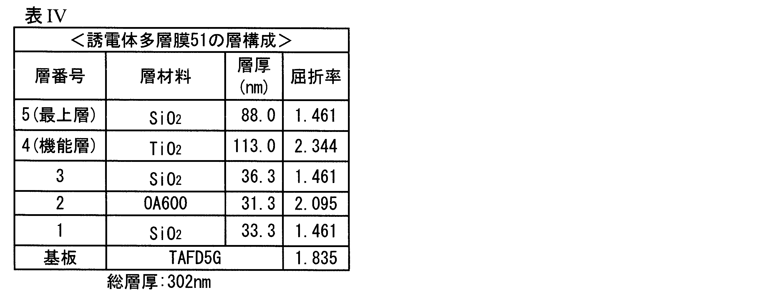
上記層厚は以下の方法によって測定した。
・装置名称:X線光電子分光分析装置(XPS)
・装置型式:Quantera SXM
・装置メーカー:アルバック・ファイ
・測定条件:X線源:単色化AlKα線25W-15kV
・真空度:5.0×10⁻⁸Pa
アルゴンイオンエッチングにより深さ方向分析を行う。データ処理は、アルバック・ファイ社製のMultiPakを用いた。
表IV記載の屈折率は、多層膜の各層を単層で成膜し、日立ハイテクノロジーズ社製分光光度計U-4100を用いたd線での光反射率測定を行うことで算出している。薄膜計算ソフト(Essential Macleod)(シグマ光機株式会社製)を用いて、実測した光反射率データに対してフィットするように屈折率を調整することで得られた層の屈折率を特定した。
最上層(層5)を形成した後、図20及び図21に示した細孔形成方法にしたがい、マスク材料としてAg、マスク成膜として蒸着法、金属マスク厚さ39nm、成膜温度300℃、マスク形状として葉脈状、エッチングガスCHF3、及びエッチング時間900secの条件で、図23Cで示される葉脈状の細孔で、及び表Vに記載の細孔の幅長、最大谷深さSv、細孔を除く微細構造の平均周期長、細孔面積比、算術平均粗さSa、二乗平均平方根高さSqを有する細孔を形成し、誘電体多層膜51を作製した。
開始真空度 1.33×10⁻³Pa
成膜レート 3Å/sec
エッチングには、IAD成膜装置(BES-1300、株式会社シンクロン製)を用い、下記の条件で成膜した。エッチング時間を変更することで、細孔の幅長、深さを調整した。
加速電流 500mA
APC圧力 7×10⁻²Pa
CHF3流量 100sccm
エッチング時間 900sec
〈マスクの剥離〉
細孔を形成した後、銀エッチャント(型番SEA-5、林純薬社製)を用いて、Agを剥離した。剥離は下記の条件で行った。
〔誘電体多層膜52~54、56、58~62の作製〕
誘電体多層膜51の作製において、金属マスクの成膜温度、厚さ及びエッチング条件を変化させて細孔の幅長、最大谷深さSv、細孔を除く微細構造の平均周期長、算術平均粗さRa、二乗平均平方根高さSqを制御した。また、IAD法の蒸着条件を制御して、機能層層厚、最上層層厚、総層厚及び最上層ナトリウム含有量のそれぞれを、表Vに記載のように変化させた以外は同様にして、誘電体多層膜52~54、56、58~62を作製した。
誘電体多層膜51の作製において、金属マスク厚さを30nm、成膜温度170℃として、ポーラス形状のマスクを作製し、ポーラス状の細孔を形成した以外は同様にして、表V記載の細孔の幅長、最大谷深さ、細孔を除く微細構造の平均周期長、細孔面積比、算術平均粗さSa、二乗平均平方根高さSqを有する誘電体多層膜55、57、63を作製した。
前述の原子間力顕微鏡(AFM)を用いた画像解析法2に従って、原子間力顕微鏡(AFM)としてBRUKER社製のDimension Iconを用い、プローブとしては、同じくBRUKER社製のシリコンプローブであるModel RTESPA-150を使用して、測定モードはPeak Force Tappingモードにて、最上層の細孔構造を測定した後、撮影した画像写真について、BRUKER社製のソフトを用いて、細孔幅長(nm)、最大谷深さSv(nm)、細孔を除く微細構造の平均周期長(nm)、細孔面積比率(%)、算術平均粗さSa(nm)、二乗平均平方根高さSq(nm)を測定して得られた結果を表Vに示す。
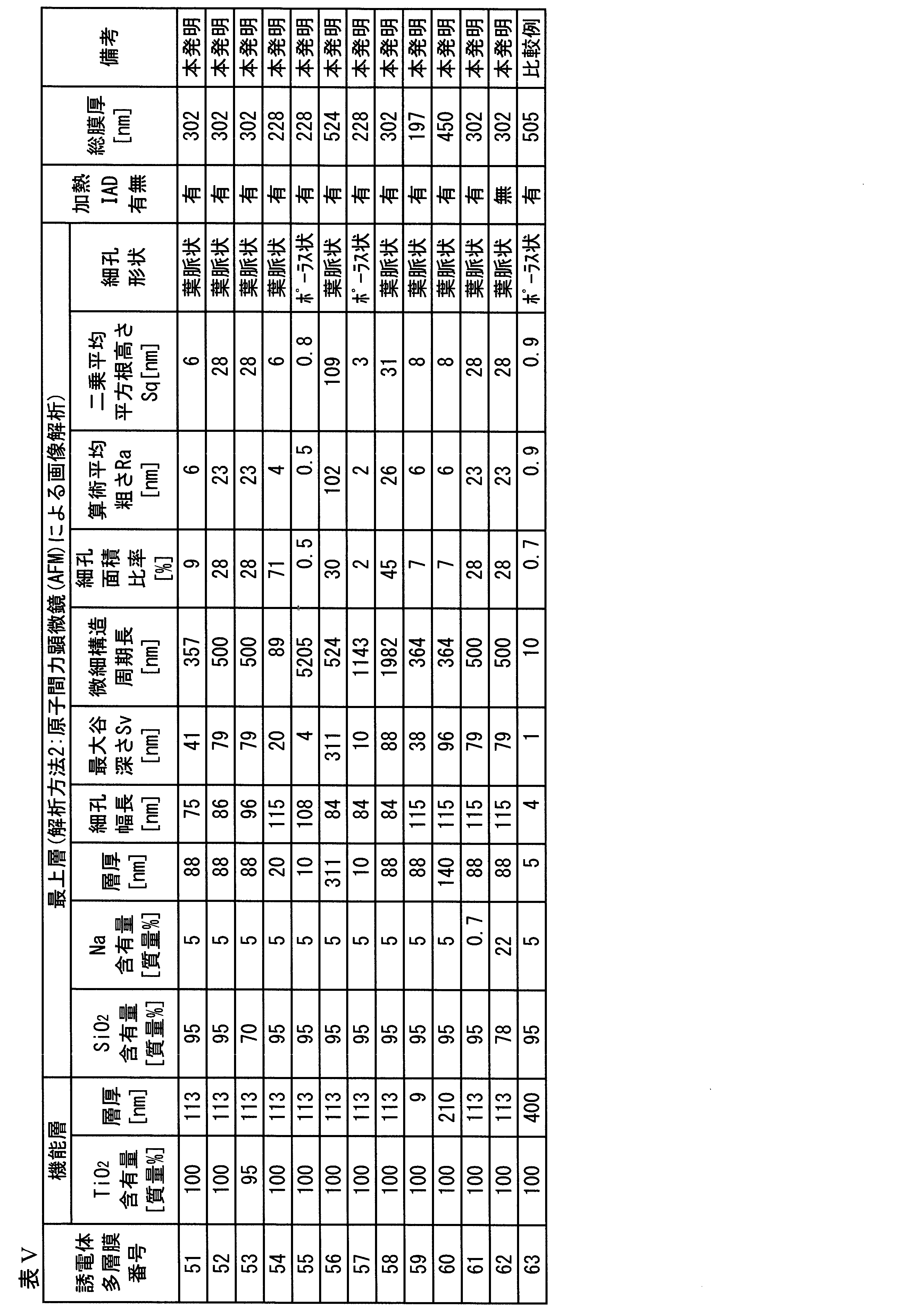
最上層の膜密度、光触媒性、高温高湿環境下での親水性(水接触角)、塩水耐性、耐傷性については、実施例1に記載の方法と同様にして評価した。
「光反射率」については、反射率測定機(USPM-RUIII)(オリンパス株式会社製)を用いて、波長域450~780nmの最大反射率で試料の光反射率(%)を評価した。ここで、基板ガラス単体の反射率より低くなっていれば反射防止効果があると評価し、特に、光反射率が2%以下である場合は、反射防止性が特に優れていると評価できる。
白板ガラスBK7(SCHOTT社製)(φ(直径)=30mm、t(厚さ)=2mm)からなる基板上に、最上層のみを形成し、NDH7000(日本電色社製)を用い、ヘイズ値(全光線透過率における拡散透過率の割合)を測定した。
△:ヘイズが、1.0%以上、5.0%未満である
×:ヘイズが、5.0%以上である
以上により得られた結果を表VIに示す。

2 チャンバー
3 ドーム
4 基板
5 蒸着源
6 蒸着物質
7 IADイオンソース
8 イオンビーム
30 細孔
31 細孔を除く微細構造
50 金属マスク
50a 金属部
50b 露出部
100 誘電体多層膜(光学部材)
101 基板
102、104 低屈折率層
103 高屈折率層
105 機能層
106 最上層
107 積層体
Claims (30)
- 基板上に複数の層で構成された誘電体多層膜であって、
前記複数の層が、少なくとも1層の低屈折率層と、少なくとも1層の高屈折率層とを有し、
前記基板から最も遠い最上層が前記低屈折率層であり、
前記最上層の基板側に配置された前記高屈折率層が光触媒機能を有する金属酸化物を含有する機能層であり、
前記最上層が親水機能を有する金属酸化物を含有する親水性層であり、かつ、前記機能層の表面を部分的に露出させる細孔を有し、
前記細孔の幅長の平均値が5nm以上であることを特徴とする誘電体多層膜。 - 基板上に複数の層で構成された誘電体多層膜であって、
前記複数の層が、少なくとも1層の低屈折率層と、少なくとも1層の高屈折率層とを有し、
前記基板から最も遠い最上層が前記低屈折率層であり、
前記最上層の基板側に配置された前記高屈折率層が光触媒機能を有する金属酸化物を含有する機能層であり、
前記最上層が親水機能を有する金属酸化物を含有する親水性層であり、 かつ、前記機
能層の表面を部分的に露出させる細孔を有し、
前記細孔の深さの平均値が10~300nmの範囲内であり、かつ、前記細孔の幅長の平均値が5~1000nmの範囲内であることを特徴とする誘電体多層膜。 - 基板上に複数の層で構成された誘電体多層膜であって、
前記複数の層が、少なくとも1層の低屈折率層と、少なくとも1層の高屈折率層とを有し、
前記基板から最も遠い最上層が前記低屈折率層であり、
前記最上層の基板側に配置された前記高屈折率層が光触媒機能を有する金属酸化物を含有する機能層であり、
前記最上層が親水機能を有する金属酸化物を含有する親水性層であり、かつ、前記機能層の表面を部分的に露出させる細孔を有し、
前記細孔の最大谷深さSvが10~300nmの範囲内であり、かつ、
前記細孔の幅長の平均値が5~1000nmの範囲内であることを特徴とする誘電体多層膜。 - 基板上に複数の層で構成された誘電体多層膜であって、
前記複数の層が、少なくとも1層の低屈折率層と、少なくとも1層の高屈折率層とを有し、
前記基板から最も遠い最上層が前記低屈折率層であり、
前記最上層の基板側に配置された前記高屈折率層が光触媒機能を有する金属酸化物を含有する機能層であり、
前記最上層が親水機能を有する金属酸化物を含有する親水性層であり、かつ、前記機能層の表面を部分的に露出させる細孔を有し、
前記細孔を除く微細構造部分の平均周期長が、20~5000nmの範囲内であることを特徴とする誘電体多層膜。 - 基板上に複数の層で構成された誘電体多層膜であって、
前記複数の層が、少なくとも1層の低屈折率層と、少なくとも1層の高屈折率層とを有し、
前記基板から最も遠い最上層が前記低屈折率層であり、
前記最上層の基板側に配置された前記高屈折率層が光触媒機能を有する金属酸化物を含有する機能層であり、
前記最上層が親水機能を有する金属酸化物を含有する親水性層であり、かつ、前記機能層の表面を部分的に露出させる細孔を有し、
前記最上層の表面積に対する前記細孔を法線方向から観察したときの前記最上層の表面における細孔の面積比率が、1~70%の範囲内であることを特徴とする誘電体多層膜。 - 基板上に複数の層で構成された誘電体多層膜であって、
前記複数の層が、少なくとも1層の低屈折率層と、少なくとも1層の高屈折率層とを有し、
前記基板から最も遠い最上層が前記低屈折率層であり、
前記最上層の基板側に配置された前記高屈折率層が光触媒機能を有する金属酸化物を含有する機能層であり、
前記最上層が親水機能を有する金属酸化物を含有する親水性層であり、かつ、前記機能層の表面を部分的に露出させる細孔を有し、
前記最上層の表面が、算術平均粗さSaが1~100nmの範囲内である、又は二乗平均平方根高さSqが1~100nmの範囲内であることを特徴とする誘電体多層膜。 - 基板上に複数の層で構成された誘電体多層膜であって、
前記複数の層が、少なくとも1層の低屈折率層と、少なくとも1層の高屈折率層とを有し、
前記基板から最も遠い最上層が前記低屈折率層であり、
前記最上層の基板側に配置された前記高屈折率層が光触媒機能を有する金属酸化物を含有する機能層であり、
前記最上層が、親水機能を有する金属酸化物を含有する親水性層であり、かつ、前記機能層の表面を部分的に露出させる細孔を有し、
前記最上層が、葉脈状構造を有する形状であることを特徴とする誘電体多層膜。 - 前記機能層が、TiO2を含有することを特徴とする請求項1から請求項7までのいずれか一項に記載の誘電体多層膜。
- 前記最上層が、SiO2を含有することを特徴とする請求項1から請求項8までのいずれか一項に記載の誘電体多層膜。
- 前記誘電体多層膜の総層厚が、500nm以下であることを特徴とする請求項1から請求項9までのいずれか一項に記載の誘電体多層膜。
- 前記機能層の層厚が、10~200nmの範囲内であることを特徴とする請求項1から請求項10までのいずれか一項に記載の誘電体多層膜。
- 前記最上層が、電気陰性度がSiより小さい元素を含有していることを特徴とする請求項1から請求項11までのいずれか一項に記載の誘電体多層膜。
- 前記最上層が、ナトリウム元素を含有していることを特徴とする請求項1から請求項12までのいずれか一項に記載の誘電体多層膜。
- 前記最上層の膜密度が、98%以上であることを特徴とする請求項1から請求項13までのいずれか一項に記載の誘電体多層膜。
- 前記最上層が、イオンアシスト蒸着によって形成されたことを特徴とする請求項1から請求項14までのいずれか一項に記載の誘電体多層膜。
- 請求項1及び請求項8から請求項15までのいずれか一項に記載の誘電体多層膜を製造する誘電体多層膜の製造方法であって、
前記複数の層として、少なくとも1層の低屈折率層と、少なくとも1層の高屈折率層とを形成する工程と、
前記高屈折率層として光触媒機能を有する金属酸化物を含有する機能層を形成する工程と、
前記基板から最も遠い最上層として、親水機能を有する金属酸化物を含有する親水性層を形成する工程と、かつ、
前記最上層に、細孔として、前記機能層の表面を部分的に露出させる、幅長の平均値が5nm以上である細孔を形成する工程と、を有することを特徴とする誘電体多層膜の製造方法。 - 請求項2及び請求項8から請求項15までのいずれか一項に記載の誘電体多層膜を製造する誘電体多層膜の製造方法であって、
前記複数の層として、少なくとも1層の低屈折率層と、少なくとも1層の高屈折率層とを形成する工程と、
前記高屈折率層として光触媒機能を有する金属酸化物を含有する機能層を形成する工程と、
前記基板から最も遠い最上層として、親水機能を有する金属酸化物を含有する親水性層を形成する工程と、かつ、
前記最上層に、深さの平均値が10~300nmの範囲内であり、幅長の平均値が5~1000nmの範囲内であり、かつ前記機能層の表面を部分的に露出させる細孔を形成する工程と、を有することを特徴とする誘電体多層膜の製造方法。 - 請求項3及び請求項8から請求項15までのいずれか一項に記載の誘電体多層膜を製造する誘電体多層膜の製造方法であって、
前記複数の層として、少なくとも1層の低屈折率層と、少なくとも1層の高屈折率層とを形成する工程と、
前記高屈折率層として光触媒機能を有する金属酸化物を含有する機能層を形成する工程と、
前記基板から最も遠い最上層として、親水機能を有する金属酸化物を含有する親水性層を形成する工程と、かつ、
前記最上層に、最大谷深さSvが10~300nmの範囲内であり、幅長の平均値が5~1000nmの範囲内であり、かつ前記機能層の表面を部分的に露出させる細孔を形成する工程と、を有することを特徴とする誘電体多層膜の製造方法。 - 請求項4及び請求項8から請求項15までのいずれか一項に記載の誘電体多層膜を製造する誘電体多層膜の製造方法であって、
前記複数の層として、少なくとも1層の低屈折率層と、少なくとも1層の高屈折率層とを形成する工程と、
前記高屈折率層として光触媒機能を有する金属酸化物を含有する機能層を形成する工程と、
前記基板から最も遠い最上層として、親水機能を有する金属酸化物を含有する親水性層を形成する工程と、かつ、
前記最上層に、前記機能層の表面を部分的に露出させる当該細孔を形成し、かつ当該細孔を除く微細構造部分の平均周期長が、20~5000nmの範囲内とする工程と、を有することを特徴とする誘電体多層膜の製造方法。 - 請求項5及び請求項8から請求項15までのいずれか一項に記載の誘電体多層膜を製造する誘電体多層膜の製造方法であって、
前記複数の層として、少なくとも1層の低屈折率層と、少なくとも1層の高屈折率層とを形成する工程と、
前記高屈折率層として光触媒機能を有する金属酸化物を含有する機能層を形成する工程と、
前記基板から最も遠い最上層として、親水機能を有する金属酸化物を含有する親水性層を形成する工程と、かつ、
前記最上層に、前記機能層の表面を部分的に露出させる当該細孔を形成し、かつ前記最上層の表面積に対する細孔を法線方向から観察したときの総面積が1~70%の範囲内と工程と、を有することを特徴とする誘電体多層膜の製造方法。 - 請求項6及び請求項8から請求項15までのいずれか一項に記載の誘電体多層膜を製造する誘電体多層膜の製造方法であって、
前記複数の層として、少なくとも1層の低屈折率層と、少なくとも1層の高屈折率層とを形成する工程と、
前記高屈折率層として光触媒機能を有する金属酸化物を含有する機能層を形成する工程と、
前記基板から最も遠い最上層として、親水機能を有する金属酸化物を含有する親水性層を形成する工程と、かつ、
前記最上層に、算術平均粗さSaが1~100nmの範囲内であり、又は二乗平均平方根高さSqが1~100nmの範囲内であり、かつ前記機能層の表面を部分的に露出させる細孔を形成する工程と、を有することを特徴とする誘電体多層膜の製造方法。 - 請求項7から請求項15までのいずれか一項に記載の誘電体多層膜を製造する誘電体多層膜の製造方法であって、
前記複数の層として、少なくとも1層の低屈折率層と、少なくとも1層の高屈折率層とを形成する工程と、
前記高屈折率層として光触媒機能を有する金属酸化物を含有する機能層を形成する工程と、
前記基板から最も遠い最上層として、親水機能を有する金属酸化物を含有する親水性層を形成する工程と、かつ、
前記最上層に、前記機能層の表面を部分的に露出させる当該細孔を形成し、かつ当該最上層が葉脈状構造を有する形状にする工程と、を有することを特徴とする誘電体多層膜の製造方法。 - 前記細孔を形成する工程において、
前記最上層を形成した後、前記最上層の表面に金属マスクを形成する工程と、かつ、
前記最上層に前記金属マスクを介してエッチングによって前記細孔を形成する工程と、
を有することを特徴とする請求項16から請求項22までのいずれか一項に記載の誘電体多層膜の製造方法。 - 前記金属マスクを形成する工程において、
当該金属マスクとして粒子状構造、葉脈状構造又はポーラス状構造を形成し、ドライエッチングによって前記細孔を形成する工程を有することを特徴とする請求項23に記載の誘電体多層膜の製造方法。 - 前記金属マスクの金属として銀を用い、成膜温度を20℃~400℃の範囲内、厚さを1~100nmの範囲内に制御することを特徴とする請求項23又は請求項24に記載の誘電体多層膜の製造方法。
- 前記誘電体多層膜を、イオンアシスト蒸着又はスパッタリングで成膜する工程を有することを特徴とする請求項16から請求項25までのいずれか一項に記載の誘電体多層膜の製造方法。
- 前記イオンアシスト蒸着する際に、300℃以上の熱を加えることを特徴とする請求項26に記載の誘電体多層膜の製造方法。
- 請求項1から請求項15までのいずれか一項に記載の誘電体多層膜を具備することを特徴とする光学部材。
- 前記光学部材が、レンズ、抗菌カバー部材、防カビコーティング部材又はミラーであることを特徴とする請求項28に記載の光学部材。
- 前記光学部材が、車載用レンズであることを特徴とする請求項28に記載の光学部材。
Priority Applications (4)
| Application Number | Priority Date | Filing Date | Title |
|---|---|---|---|
| US17/312,929 US12259522B2 (en) | 2018-12-21 | 2019-11-27 | Dielectric multilayer film, method for producing same and optical member using same |
| CN201980082853.5A CN113167928B (zh) | 2018-12-21 | 2019-11-27 | 电介质多层膜、其制造方法和使用其的光学构件 |
| EP19900819.4A EP3901671A4 (en) | 2018-12-21 | 2019-11-27 | DIELECTRIC MULTILAYER FILM, METHOD OF MAKING THEREOF AND OPTICAL ELEMENT USING THEREOF |
| JP2020561247A JP7375772B2 (ja) | 2018-12-21 | 2019-11-27 | 誘電体多層膜、その製造方法及びそれを用いた光学部材 |
Applications Claiming Priority (4)
| Application Number | Priority Date | Filing Date | Title |
|---|---|---|---|
| JP2018239790 | 2018-12-21 | ||
| JP2018-239790 | 2018-12-21 | ||
| JP2019120511 | 2019-06-27 | ||
| JP2019-120511 | 2019-06-27 |
Publications (1)
| Publication Number | Publication Date |
|---|---|
| WO2020129558A1 true WO2020129558A1 (ja) | 2020-06-25 |
Family
ID=71101108
Family Applications (1)
| Application Number | Title | Priority Date | Filing Date |
|---|---|---|---|
| PCT/JP2019/046288 Ceased WO2020129558A1 (ja) | 2018-12-21 | 2019-11-27 | 誘電体多層膜、その製造方法及びそれを用いた光学部材 |
Country Status (5)
| Country | Link |
|---|---|
| US (1) | US12259522B2 (ja) |
| EP (1) | EP3901671A4 (ja) |
| JP (1) | JP7375772B2 (ja) |
| CN (1) | CN113167928B (ja) |
| WO (1) | WO2020129558A1 (ja) |
Cited By (2)
| Publication number | Priority date | Publication date | Assignee | Title |
|---|---|---|---|---|
| WO2022101428A3 (en) * | 2020-11-13 | 2022-06-23 | Carl Zeiss Vision International Gmbh | Spectacle lens with antibacterial and/or antiviral properties and method for manufacturing the same |
| US12596408B2 (en) | 2022-12-22 | 2026-04-07 | Samsung Display Co., Ltd. | Display device and method for manufacturing the same |
Families Citing this family (3)
| Publication number | Priority date | Publication date | Assignee | Title |
|---|---|---|---|---|
| US12024767B2 (en) * | 2018-12-21 | 2024-07-02 | Konica Minolta, Inc. | Dielectric film, method for producing same and optical member using same |
| JP2023070405A (ja) * | 2021-11-09 | 2023-05-19 | コニカミノルタ株式会社 | 機能性膜及び機能性膜の製造方法 |
| CN116040965B (zh) * | 2023-01-31 | 2024-02-27 | 宁波启朴芯微系统技术有限公司 | 一种宽频减反膜及其制备方法和应用 |
Citations (18)
| Publication number | Priority date | Publication date | Assignee | Title |
|---|---|---|---|---|
| JPS5211321B2 (ja) * | 1972-04-11 | 1977-03-30 | ||
| JPH0432558A (ja) * | 1990-05-29 | 1992-02-04 | Nippon Shinku Kogaku Kk | 誘電体多層膜の製造法 |
| JPH0811631A (ja) * | 1994-06-29 | 1996-01-16 | Murakami Kaimeidou:Kk | 車両用ミラー |
| JPH09202651A (ja) * | 1996-01-25 | 1997-08-05 | Central Glass Co Ltd | 親水性被膜及びその形成法 |
| JPH1036144A (ja) | 1996-07-26 | 1998-02-10 | Murakami Corp | 防曇素子 |
| JPH1184102A (ja) * | 1997-04-09 | 1999-03-26 | Canon Inc | 防曇性被覆およびこれを用いた光学部品 |
| JP2000160331A (ja) | 1998-02-16 | 2000-06-13 | Asahi Glass Co Ltd | 酸化物膜、その形成方法、スパッタリングタ―ゲットおよび積層体 |
| JP2000308860A (ja) * | 1999-02-24 | 2000-11-07 | Toto Ltd | 複合材の清浄化方法及びセルフクリーニング性複合材機構 |
| JP2003287601A (ja) * | 2002-03-27 | 2003-10-10 | Murakami Corp | 複合材 |
| JP2004068109A (ja) | 2002-08-08 | 2004-03-04 | Nippon Sheet Glass Co Ltd | 反応性スパッタリング用ターゲットおよびそれを用いて成膜した光学薄膜 |
| JP2008168610A (ja) * | 2006-12-13 | 2008-07-24 | National Institute Of Advanced Industrial & Technology | ナノ構造体を有する光学素子用成形型、ナノ構造体用成形型、その製造方法および光学素子 |
| JP2008270416A (ja) * | 2007-04-18 | 2008-11-06 | Sanken Electric Co Ltd | 物体に粗面を形成する方法 |
| JP2008274409A (ja) * | 2007-03-30 | 2008-11-13 | Fujifilm Corp | 防曇膜の形成方法 |
| JP2013047361A (ja) | 2011-08-29 | 2013-03-07 | Mitsubishi Materials Corp | スパッタリングターゲット及びその製造方法並びに該ターゲットを用いた薄膜、該薄膜を備える薄膜シート、積層シート |
| JP2015227904A (ja) * | 2014-05-30 | 2015-12-17 | 旭硝子株式会社 | 反射防止構造体およびその製造方法 |
| WO2017056598A1 (ja) * | 2015-09-29 | 2017-04-06 | 富士フイルム株式会社 | 親水性多層膜及びその製造方法、並びに、撮像システム |
| JP2017182065A (ja) * | 2016-03-29 | 2017-10-05 | リコーイメージング株式会社 | 光学素子及びその製造方法 |
| JP2019002036A (ja) * | 2017-06-13 | 2019-01-10 | 株式会社 高千穂 | 酸化物被膜及びその酸化物被膜を備える構造体 |
Family Cites Families (17)
| Publication number | Priority date | Publication date | Assignee | Title |
|---|---|---|---|---|
| GB1428769A (en) * | 1972-02-28 | 1976-03-17 | Nippon Sheet Glass Co Ltd | Surface protective coating on an article |
| JPS5211321A (en) * | 1975-07-17 | 1977-01-28 | Nissan Motor Co Ltd | Opening and closing time regulation device of suction and exhaust valv e in internal combustion engine |
| US6287683B1 (en) * | 1997-04-09 | 2001-09-11 | Canon Kabushiki Kaisha | Anti-fogging coating and optical part using the same |
| JP2000053449A (ja) | 1998-08-06 | 2000-02-22 | Murakami Corp | 防曇鏡およびその製造方法 |
| FR2793889B1 (fr) * | 1999-05-20 | 2002-06-28 | Saint Gobain Vitrage | Substrat transparent a revetement anti-reflets |
| JP2001033607A (ja) * | 1999-07-23 | 2001-02-09 | Toto Ltd | 親水性鏡、その形成用組成物、及びその製造方法 |
| JP2001286754A (ja) * | 2000-04-06 | 2001-10-16 | Nippon Sheet Glass Co Ltd | 光触媒膜付き基板およびその製造方法 |
| JP3662807B2 (ja) | 2000-04-10 | 2005-06-22 | トアス株式会社 | 手押し台車 |
| JP3372527B2 (ja) * | 2000-05-17 | 2003-02-04 | 株式会社村上開明堂 | 複合材 |
| JP2002301378A (ja) * | 2001-04-04 | 2002-10-15 | Mitsui Eng & Shipbuild Co Ltd | 光触媒モジュール、その製造方法、光触媒反応装置 |
| TWI276613B (en) * | 2002-04-05 | 2007-03-21 | Murakami Corp | Composite material |
| US7910220B2 (en) * | 2007-07-25 | 2011-03-22 | Alcoa Inc. | Surfaces and coatings for the removal of carbon dioxide |
| JP5804996B2 (ja) * | 2012-03-27 | 2015-11-04 | 中央自動車工業株式会社 | 有機基材用防曇防汚剤及び当該防曇防汚剤で有機基材を被覆する方法 |
| JP6103642B2 (ja) | 2012-08-01 | 2017-03-29 | 株式会社 高千穂 | シラス構造体およびシラス構造体の製造方法 |
| SG11201701948SA (en) * | 2014-09-11 | 2017-04-27 | Agency Science Tech & Res | Amorphous metal oxide films |
| JP2020024238A (ja) * | 2016-12-14 | 2020-02-13 | コニカミノルタ株式会社 | 光学素子 |
| US10274647B2 (en) * | 2017-05-18 | 2019-04-30 | GM Global Technology Operations LLC | Self-cleaning film system and article |
-
2019
- 2019-11-27 JP JP2020561247A patent/JP7375772B2/ja active Active
- 2019-11-27 CN CN201980082853.5A patent/CN113167928B/zh active Active
- 2019-11-27 US US17/312,929 patent/US12259522B2/en active Active
- 2019-11-27 EP EP19900819.4A patent/EP3901671A4/en active Pending
- 2019-11-27 WO PCT/JP2019/046288 patent/WO2020129558A1/ja not_active Ceased
Patent Citations (18)
| Publication number | Priority date | Publication date | Assignee | Title |
|---|---|---|---|---|
| JPS5211321B2 (ja) * | 1972-04-11 | 1977-03-30 | ||
| JPH0432558A (ja) * | 1990-05-29 | 1992-02-04 | Nippon Shinku Kogaku Kk | 誘電体多層膜の製造法 |
| JPH0811631A (ja) * | 1994-06-29 | 1996-01-16 | Murakami Kaimeidou:Kk | 車両用ミラー |
| JPH09202651A (ja) * | 1996-01-25 | 1997-08-05 | Central Glass Co Ltd | 親水性被膜及びその形成法 |
| JPH1036144A (ja) | 1996-07-26 | 1998-02-10 | Murakami Corp | 防曇素子 |
| JPH1184102A (ja) * | 1997-04-09 | 1999-03-26 | Canon Inc | 防曇性被覆およびこれを用いた光学部品 |
| JP2000160331A (ja) | 1998-02-16 | 2000-06-13 | Asahi Glass Co Ltd | 酸化物膜、その形成方法、スパッタリングタ―ゲットおよび積層体 |
| JP2000308860A (ja) * | 1999-02-24 | 2000-11-07 | Toto Ltd | 複合材の清浄化方法及びセルフクリーニング性複合材機構 |
| JP2003287601A (ja) * | 2002-03-27 | 2003-10-10 | Murakami Corp | 複合材 |
| JP2004068109A (ja) | 2002-08-08 | 2004-03-04 | Nippon Sheet Glass Co Ltd | 反応性スパッタリング用ターゲットおよびそれを用いて成膜した光学薄膜 |
| JP2008168610A (ja) * | 2006-12-13 | 2008-07-24 | National Institute Of Advanced Industrial & Technology | ナノ構造体を有する光学素子用成形型、ナノ構造体用成形型、その製造方法および光学素子 |
| JP2008274409A (ja) * | 2007-03-30 | 2008-11-13 | Fujifilm Corp | 防曇膜の形成方法 |
| JP2008270416A (ja) * | 2007-04-18 | 2008-11-06 | Sanken Electric Co Ltd | 物体に粗面を形成する方法 |
| JP2013047361A (ja) | 2011-08-29 | 2013-03-07 | Mitsubishi Materials Corp | スパッタリングターゲット及びその製造方法並びに該ターゲットを用いた薄膜、該薄膜を備える薄膜シート、積層シート |
| JP2015227904A (ja) * | 2014-05-30 | 2015-12-17 | 旭硝子株式会社 | 反射防止構造体およびその製造方法 |
| WO2017056598A1 (ja) * | 2015-09-29 | 2017-04-06 | 富士フイルム株式会社 | 親水性多層膜及びその製造方法、並びに、撮像システム |
| JP2017182065A (ja) * | 2016-03-29 | 2017-10-05 | リコーイメージング株式会社 | 光学素子及びその製造方法 |
| JP2019002036A (ja) * | 2017-06-13 | 2019-01-10 | 株式会社 高千穂 | 酸化物被膜及びその酸化物被膜を備える構造体 |
Non-Patent Citations (1)
| Title |
|---|
| See also references of EP3901671A4 |
Cited By (2)
| Publication number | Priority date | Publication date | Assignee | Title |
|---|---|---|---|---|
| WO2022101428A3 (en) * | 2020-11-13 | 2022-06-23 | Carl Zeiss Vision International Gmbh | Spectacle lens with antibacterial and/or antiviral properties and method for manufacturing the same |
| US12596408B2 (en) | 2022-12-22 | 2026-04-07 | Samsung Display Co., Ltd. | Display device and method for manufacturing the same |
Also Published As
| Publication number | Publication date |
|---|---|
| CN113167928A (zh) | 2021-07-23 |
| EP3901671A4 (en) | 2022-02-23 |
| JP7375772B2 (ja) | 2023-11-08 |
| CN113167928B (zh) | 2023-10-27 |
| US20220128738A1 (en) | 2022-04-28 |
| US12259522B2 (en) | 2025-03-25 |
| JPWO2020129558A1 (ja) | 2021-11-04 |
| EP3901671A1 (en) | 2021-10-27 |
Similar Documents
| Publication | Publication Date | Title |
|---|---|---|
| JP7375772B2 (ja) | 誘電体多層膜、その製造方法及びそれを用いた光学部材 | |
| EP4300141A1 (en) | Functional film, manufacturing method for funcitonal film, optical device, ink jet head, and mold | |
| EP3875997B1 (en) | Dielectric film, method for producing same and optical member using same | |
| JP7279713B2 (ja) | 光学薄膜、光学部材及び光学薄膜の製造方法 | |
| US20200166672A1 (en) | Optical member and producing method of optical member | |
| US11780728B2 (en) | Forming method of thin layer | |
| JP7476564B2 (ja) | 超親水膜とその製造方法及び光学部材 | |
| US20230251401A1 (en) | Hydrophilic film manufacturing method, hydrophilic film, and optical member | |
| US20200165716A1 (en) | Film forming method and film forming apparatus | |
| CN116657086A (zh) | 功能性膜和功能性膜的制造方法 | |
| WO2021111813A1 (ja) | 光学部材及びその製造方法 | |
| TWI750642B (zh) | 微結構體之製造方法及微結構體之製造裝置 | |
| WO2018216540A1 (ja) | 親水性反射防止膜付きレンズ及びその製造方法 | |
| US20250189698A1 (en) | Multilayer film, optical member including multilayer film, and method for producing multilayer film | |
| EP1802452B1 (en) | Optical element with an opaque chrome coating having an aperture and method of making same | |
| EP4385960A1 (en) | Manufacturing method of the functional membrane and the functional membrane | |
| WO2025126699A1 (ja) | 機能性膜、機能性膜の製造方法及び積層体 |
Legal Events
| Date | Code | Title | Description |
|---|---|---|---|
| 121 | Ep: the epo has been informed by wipo that ep was designated in this application |
Ref document number: 19900819 Country of ref document: EP Kind code of ref document: A1 |
|
| ENP | Entry into the national phase |
Ref document number: 2020561247 Country of ref document: JP Kind code of ref document: A |
|
| NENP | Non-entry into the national phase |
Ref country code: DE |
|
| ENP | Entry into the national phase |
Ref document number: 2019900819 Country of ref document: EP Effective date: 20210721 |
|
| WWG | Wipo information: grant in national office |
Ref document number: 17312929 Country of ref document: US |