WO2020153322A1 - 電界センサ - Google Patents
電界センサ Download PDFInfo
- Publication number
- WO2020153322A1 WO2020153322A1 PCT/JP2020/001833 JP2020001833W WO2020153322A1 WO 2020153322 A1 WO2020153322 A1 WO 2020153322A1 JP 2020001833 W JP2020001833 W JP 2020001833W WO 2020153322 A1 WO2020153322 A1 WO 2020153322A1
- Authority
- WO
- WIPO (PCT)
- Prior art keywords
- light
- electric field
- gain
- field sensor
- light source
- Prior art date
- Legal status (The legal status is an assumption and is not a legal conclusion. Google has not performed a legal analysis and makes no representation as to the accuracy of the status listed.)
- Ceased
Links
Images




Classifications
-
- G—PHYSICS
- G01—MEASURING; TESTING
- G01R—MEASURING ELECTRIC VARIABLES; MEASURING MAGNETIC VARIABLES
- G01R15/00—Details of measuring arrangements of the types provided for in groups G01R17/00 - G01R29/00, G01R33/00 - G01R33/26 or G01R35/00
- G01R15/14—Adaptations providing voltage or current isolation, e.g. for high-voltage or high-current networks
- G01R15/24—Adaptations providing voltage or current isolation, e.g. for high-voltage or high-current networks using light-modulating devices
- G01R15/241—Adaptations providing voltage or current isolation, e.g. for high-voltage or high-current networks using light-modulating devices using electro-optical modulators, e.g. electro-absorption
- G01R15/242—Adaptations providing voltage or current isolation, e.g. for high-voltage or high-current networks using light-modulating devices using electro-optical modulators, e.g. electro-absorption based on the Pockels effect, i.e. linear electro-optic effect
-
- G—PHYSICS
- G01—MEASURING; TESTING
- G01R—MEASURING ELECTRIC VARIABLES; MEASURING MAGNETIC VARIABLES
- G01R29/00—Arrangements for measuring or indicating electric quantities not covered by groups G01R19/00 - G01R27/00
- G01R29/12—Measuring electrostatic fields or voltage-potential
- G01R29/14—Measuring field distribution
-
- G—PHYSICS
- G01—MEASURING; TESTING
- G01R—MEASURING ELECTRIC VARIABLES; MEASURING MAGNETIC VARIABLES
- G01R15/00—Details of measuring arrangements of the types provided for in groups G01R17/00 - G01R29/00, G01R33/00 - G01R33/26 or G01R35/00
- G01R15/14—Adaptations providing voltage or current isolation, e.g. for high-voltage or high-current networks
- G01R15/24—Adaptations providing voltage or current isolation, e.g. for high-voltage or high-current networks using light-modulating devices
- G01R15/241—Adaptations providing voltage or current isolation, e.g. for high-voltage or high-current networks using light-modulating devices using electro-optical modulators, e.g. electro-absorption
-
- G—PHYSICS
- G01—MEASURING; TESTING
- G01R—MEASURING ELECTRIC VARIABLES; MEASURING MAGNETIC VARIABLES
- G01R29/00—Arrangements for measuring or indicating electric quantities not covered by groups G01R19/00 - G01R27/00
- G01R29/08—Measuring electromagnetic field characteristics
- G01R29/0864—Measuring electromagnetic field characteristics characterised by constructional or functional features
- G01R29/0878—Sensors; antennas; probes; detectors
- G01R29/0885—Sensors; antennas; probes; detectors using optical probes, e.g. electro-optical, luminescent, glow discharge, or optical interferometers
Definitions
- the present invention relates to an electric field sensor.
- the present application claims priority based on Japanese Patent Application No. 2019-008252 filed in Japan on January 22, 2019, the content of which is incorporated herein.
- the electro-optic effect is an effect in which, when an electric field is applied to the electro-optic crystal, the refractive index of light passing through the electro-optic crystal changes according to the electric field strength. Further, the change of the refractive index gives a phase change of the light wave passing through the optical crystal.
- the electric field applied to the electro-optic crystal can be measured by measuring the change in phase (for example, see Patent Documents 1 and 2).
- FIG. 7 is a diagram showing a configuration example and an operation example of an electric field sensor 900 utilizing the electro-optical effect according to the conventional technique.
- the electric field sensor 900 includes a laser light source 901, an analyzer 902, a ⁇ /4 wavelength plate 903, an electric field generation source 904, an electro-optic crystal 905, and a ⁇ /2 wavelength plate 906. It has a polarization beam splitter 907, a photodetector 908, a photodetector 909, and a differential amplifier 910.
- the laser light source 901 is, for example, a semiconductor laser.
- the analyzer 902 emits linearly polarized light in the light rays incident from the laser light source 901.
- the ⁇ /4 wave plate 903 polarizes the light beam incident from the analyzer 902 into circularly polarized light and emits it.
- the electric field generation source 904 generates an electric field with respect to the electro-optic crystal 905.
- the electro-optic crystal 905 changes the polarization state by changing the birefringence according to the electric field strength applied by the electric field generation source 904.
- the electro-optic crystal 905 emits an elliptically polarized light beam whose azimuth of the elliptic axis is inclined at 45 degrees. The ellipticity of elliptically polarized light changes depending on the strength of the electric field.
- the ⁇ /2 wave plate 906 changes the light beam emitted from the electro-optic crystal 905 into elliptically polarized light whose azimuth of elliptically polarized light is 0 degree while maintaining the ellipticity of elliptically polarized light.
- the polarization beam splitter 907 splits the elliptically polarized light beam emitted from the ⁇ /2 wave plate 906 with the azimuth of the elliptically polarized light of 0 degrees into P waves and S waves.
- the photodetector 908 converts the P wave incident from the polarization beam splitter 907 into an electric signal, and outputs the converted electric signal of the P wave component to one input end of the differential amplifier 910.
- the photodetector 909 converts the S wave incident from the polarization beam splitter 907 into an electric signal, and outputs the converted electric signal of the S wave component to the other input end of the differential amplifier 910.
- the differential amplifier 910 amplifies the differential component of the electric signals of the P wave component and the S wave component, and outputs the amplified electric signal to a signal processing device (not shown). It should be noted that since the temporal changes in the intensities of the P wave and the S wave have opposite phases, the electric field intensity signal is doubled by the differential amplifier 910.
- the transmittance T P of the P wave has a phase difference ⁇ . It is expressed by the following equation (1). Further, the transmittance T S of the S wave is expressed by the following equation (2) using the phase difference ⁇ .
- the transmittance T P (t of the P wave is T P (t ) Is expressed by the following equation (3).
- the transmittance T S (t) of the S wave is represented by the following equation (4).
- FIG. 8 is a diagram for explaining the operation when the P wave transmittance T P (t) and the S wave transmittance T S (t) are in a differential balance.
- the horizontal axis represents the phase difference ⁇ and the vertical axis represents the transmittance T.
- reference numeral g922 represents a change due to the P wave.
- reference numeral g923 represents a change due to the S wave.
- the graph indicated by reference sign g924 represents the change in the light intensity of the P wave and the S wave when the average phase difference is 0.
- Reference numeral g925 represents a change in the phase difference when the average phase difference is zero.
- the laser light has intensity fluctuation (noise)
- it is ideally superimposed on the waveforms of the P-wave transmittance T P (t) and the S-wave transmittance T S (t) in phase.
- the magnitude of the noise is proportional to the average optical power T PO of the P wave and the average optical power P SO of the S wave.
- T PO T SO
- the noise component can be canceled by the differential amplifier 910.
- FIG. 9 the phase shifts as shown in FIG. 9 due to the optical rotatory power and deviation of the optical component including the electro-optic crystal 905, the angular deviation of the wave plate, and the like.
- FIG. 9 is a diagram for explaining the operation when the differential balance between the transmittance T P (t) of the P wave and the transmittance T S (t) of the S wave is deviated.
- the horizontal axis represents the phase difference ⁇ and the vertical axis represents the transmittance T.
- reference numeral g932 represents a change due to the P wave.
- reference numeral g933 represents a change due to the S wave.
- the graph indicated by reference sign g934 represents changes in the light intensity of the P wave and the S wave in which the offset ⁇ 0 is added to the phase difference.
- Reference numeral g935 represents a change in the phase difference in which the offset ⁇ 0 is added to the phase difference.
- FIG. 10 is a diagram showing a configuration example in which the wave plate is rotated to adjust the differential balance.
- the electric field sensor 900a includes a laser light source 901, an analyzer 902, a ⁇ /4 wavelength plate 903a, an electric field generation source 904, an electro-optic crystal 905, and a ⁇ /2 wavelength plate 906b. , A polarization beam splitter 907, a photo detector 908, a photo detector 909, and a differential amplifier 910. Even when the electric field is not applied to the electro-optic crystal 905, the output of the differential amplifier 910 does not become 0 due to the difference between the outputs of the photo detector 908 and the photo detector 909 due to the shift of the optical balance point. Therefore, in the electric field sensor 900a, the ⁇ /4 wave plate 903a and the ⁇ /2 wave plate 906b are rotated to optically adjust the balance between the P wave and the S wave.
- One embodiment of the present invention is made in view of the above circumstances, and in an electric field sensor utilizing an electro-optical effect, an electric field in which fluctuations of laser light can be eliminated by simplifying a structure as compared with a conventional electric field sensor. It is intended to provide a sensor.
- an electric field sensor (electric field sensors 100, 100A, 100B, 100C) according to one embodiment of the present invention has a light source (semiconductor laser 102) and a predetermined polarization state based on light emitted from the light source.
- An electro-optic crystal (electro-optic crystal 107) that receives light and receives an electric field emitted from the object, and a first separation unit (polarization light) that separates light emitted from the electro-optic crystal into P waves and S waves.
- a beam splitter 109), a first wave plate ( ⁇ /4 wave plate 105) for changing the phase of the light before the first splitting section, and the P-wave light, and the received light is A first light receiving section (light receiving circuit 110) for converting into an electric signal; a second light receiving section (light receiving circuit 111) for receiving the light of the S wave and converting the received light into a second electric signal; Light from the light source is generated by a differential amplifier unit (differential amplifier 112) that generates a differential signal between the first electric signal converted by the light receiving unit and the second electric signal converted by the second light receiving unit.
- a differential amplifier unit differential amplifier 112 that generates a differential signal between the first electric signal converted by the light receiving unit and the second electric signal converted by the second light receiving unit.
- a control unit (DC level measuring unit 113) that adjusts the wavelength of the light source so that the output value of the DC component of the differential amplification unit in the state of being emitted and applying an electric field to the electro-optic crystal is within a predetermined value range.
- a temperature controller 114 and a temperature controller 103).
- the electric field sensor changes the wavelength of the laser by adjusting the temperature of the light source so that the output of the differential amplification unit falls within a predetermined range.
- control unit sets the output value of the DC component of the differential amplification unit in a state where light is emitted from the light source and an electric field is applied to the electro-optic crystal to the predetermined value.
- the wavelength of the light source may be adjusted by adjusting the temperature of the light source so as to fall within the range of.
- the electric field sensor is configured such that the control unit adjusts the variation due to the optical components in the state where the electric field is applied to the electro-optic crystal.
- the fluctuation (noise) of the light intensity can be canceled by the laser.
- the balance shift is reduced and the balance point is located at an appropriate position. Therefore, according to the above configuration, the signal strength is increased as compared with the case where the balance is shifted, and the S/N is less deteriorated and the stable electric field is reduced. A measurement can be made.
- the measuring device further includes a transparent electrode (ITO 116) and a mirror (mirror 117), and the electro-optic crystal is arranged with the transparent electrode facing one surface.
- the mirror is disposed on the other surface, light in a predetermined polarization state based on the light emitted by the light source is incident from the transparent electrode, the light incident from the transparent electrode is reflected by the mirror, the reflected light May be emitted from the transparent electrode, and the light emitted from the transparent electrode may enter the separation section.
- the electric field sensor has a vertical structure, it is possible to further cancel the fluctuation (noise) of the light intensity by the laser. As a result, the balance shift is reduced and the balance point is located at an appropriate position. Therefore, according to the above configuration, the signal strength is increased as compared with the case where the balance is shifted, and the S/N is less deteriorated and the stable electric field is reduced. A measurement can be made.
- the measuring device includes a first gain variable unit (gain variable amplifier 121) that changes a first gain of the first electric signal of the first light receiving unit, and a second light receiving unit. And a second gain variable unit (gain variable amplifier 122) for changing the second gain of the second electric signal, wherein the control unit emits light from the light source and applies an electric field to the electro-optic crystal.
- the first gain of the first gain varying section and the second gain of the second gain varying section so that the output value of the DC component of the differential amplifying section in the non-operation state falls within a predetermined value range. It may be adjusted.
- the electric field sensor adjusts the variation due to the optical component in a state where the electric field is not applied to the electro-optic crystal by the first gain varying section and the second gain varying section, and the electric field is applied to the electro-optic crystal.
- the control unit adjusts the variation due to the optical components in the existing state.
- the fluctuation (noise) of the light intensity can be canceled by the laser.
- the balance shift is reduced and the balance point is located at an appropriate position. Therefore, according to the above configuration, the signal strength is increased as compared with the case where the balance is shifted, and the S/N is less deteriorated and the stable electric field is reduced. A measurement can be made.
- the electric field sensor (electric field sensor 100, 100A, 100B, 100C) according to one aspect of the present invention may measure the electric field emitted by the object using the electro-optical effect.
- the first wave plate ( ⁇ /4 wave plate 105) is arranged such that the azimuth of the optical axis of the first wave plate is inclined by a first angle with respect to a predetermined axis. May be.
- the first wave plate ( ⁇ /4 wave plate 105) is arranged in front of the electro-optic crystal (electro-optic crystal 107), and the electric field sensor (electric field sensor 100, 100B). May further include a second wave plate ( ⁇ /2 wave plate 108) that is arranged in the latter stage of the electro-optic crystal and that changes the phase of light in the latter stage of the first separation section.
- the second wave plate ( ⁇ /2 wave plate 108) according to an aspect of the present invention is arranged such that the azimuth of the optical axis of the second wave plate is inclined at a second angle with respect to the predetermined axis. May be done.
- the light source (laser light source 101) includes a laser diode chip (LD chip 102c) that emits light, a photodetector (PD 102b) that measures the light intensity of the light emitted by the laser diode chip, A thermistor (thermistor 102a) that measures the temperature of the substrate to which the laser diode chip and the photodetector are attached, and a lens (lens 102d) that condenses the light beam emitted from the laser diode chip may be provided.
- LD chip 102c laser diode chip
- PD 102b photodetector
- a thermistor thermoistor 102a
- lens lens
- the electric field sensor (electric field sensor 100A, 100C) which concerns on 1 aspect of this invention WHEREIN: The 2nd isolation
- the unit (polarizing beam splitter 115) may be further provided.
- control unit (the DC level measuring unit 113, the temperature control unit 114, and the temperature adjuster 103) according to one aspect of the present invention may adjust the gain of the first gain varying unit and the gain of the second gain varying unit to: It may be adjusted in real time.
- control unit (the DC level measuring unit 113, the temperature control unit 114, and the temperature adjuster 103) according to an aspect of the present invention emits light from the light source and generates an electric field in the electro-optic crystal (electro-optic crystal 107).
- the temperature of the light source (laser light source 101) is determined by using the output value of the DC component of the differential amplifier section (differential amplifier 112) in the state of applying the voltage and the information output by the thermistor (thermistor 102a).
- the wavelength of the light source may be adjusted by adjusting.
- the light source (laser light source 101) may include an external resonance type laser.
- the electric field sensor (100B, 100C) which concerns on 1 aspect of this invention WHEREIN: The 1st optical attenuator provided between the said 1st isolation
- the attenuation factors of the first optical attenuator and the second optical attenuator may be adjusted so that the output of the differential amplification unit falls within a predetermined range in the state where the signal is not generated.
- fluctuations in laser light can be eliminated by simplifying the configuration compared with the conventional electric field sensor.
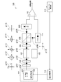
- FIG. 1 is a diagram showing a configuration example of an electric field sensor 100 according to the first embodiment.
- the electric field sensor 100 includes a laser light source 101 (light source), an analyzer 104, a ⁇ /4 wavelength plate 105 (first wavelength plate), an electric field generation source 106, and an electro-optic crystal 107. , ⁇ /2 wave plate (second wave plate), polarization beam splitter 109 (first separation unit), light receiving circuit 110 (first light receiving unit), light receiving circuit 111 (second light receiving unit), It includes a dynamic amplifier 112 (differential amplification unit), a DC level measuring unit 113 (control unit), and a temperature control unit 114 (control unit).
- a dynamic amplifier 112 differential amplification unit
- DC level measuring unit 113 control unit
- a temperature control unit 114 control unit
- the laser light source 101 includes a semiconductor laser 102 (light source) and a temperature controller 103 (control unit). As shown by reference numeral g111, in FIG. 1, the light emitted from the laser light source 101 is a transverse wave having no vibration component in the traveling direction, the magnetic field oscillation direction is the x-axis with respect to the traveling direction, and the electric field oscillation direction is Let y-axis.
- the analyzer 104 is arranged between the laser light source 101 and the ⁇ /4 wave plate 105.
- the ⁇ /4 wave plate 105 is arranged between the analyzer 104 and the electro-optic crystal 107.
- the electro-optic crystal 107 is arranged between the ⁇ /4 wave plate 105 and the ⁇ /2 wave plate 108.
- the ⁇ /2 wave plate 108 is arranged between the electro-optic crystal 107 and the polarization beam splitter 109.
- the polarization beam splitter 109 is arranged between the ⁇ /2 wave plate 108 and the light receiving circuit 110 and between the ⁇ /2 wave plate 108 and the light receiving circuit 111.
- the output terminal of the light receiving circuit 110 is connected to the first input terminal of the differential amplifier 112.
- the output end of the light receiving circuit 111 is connected to the second input terminal of the differential amplifier 112.
- the output terminal of the differential amplifier 112 outputs the processed signal to a signal processing device (not shown).
- the electric field sensor 100 obtains the amount of phase change induced by the electric field strength applied to the electro-optic crystal 107 mounted in the sensor by optical means.
- the electric field sensor 100 generates an object to be measured by applying an electric field generated by the object to be measured to the electro-optic crystal 107 to measure the output value of the differential amplifier 112 by a signal processing device (not shown). Measure the magnitude of the electric field.
- the semiconductor laser 102 is, for example, a semiconductor laser.
- the semiconductor laser 102 is driven by a laser driving unit (not shown) to emit light.
- the temperature controller 103 is attached to the semiconductor laser 102.
- the temperature controller 103 is, for example, a Peltier element.
- the temperature controller 103 adjusts the temperature of the semiconductor laser 102 under the control of the temperature controller 114.
- the analyzer 104 emits linearly polarized light (reference signs g101, g111) of the light rays incident from the laser light source 101.
- the ⁇ /4 wave plate 105 is arranged so that the azimuth of the optical axis is inclined by 45 degrees with respect to the x axis.
- the ⁇ /4 wave plate 105 polarizes the light beam incident from the analyzer 104 into circularly polarized light (reference signs g102 and g112) and outputs the polarized light.
- the ⁇ /4 wave plate 105 optically biases the light incident on the electro-optic crystal 107.
- the electric field generation source 106 generates an electric field for the electro-optic crystal 107.
- the electro-optic crystal 107 changes the polarization state by changing the birefringence according to the electric field strength applied by the electric field generation source 106.
- the electro-optic crystal 107 emits a light beam of elliptically polarized light (reference numerals g103 and g113) whose azimuth of the elliptic axis is inclined at 45 degrees.
- the ellipticity of elliptically polarized light changes depending on the strength of the electric field.
- the electro-optic crystal 107 is, for example, LiNbO3, LiTaO3, Bi12SiO20 (BSO), Bi12GeO20 (BGO), ADP, KDP, or the like.
- the ⁇ /2 wave plate 108 is arranged with the azimuth of the optical axis inclined by 22.5 degrees with respect to the x axis.
- the ⁇ /2 wave plate 108 changes the light beam emitted from the electro-optic crystal 107 into elliptically polarized light (reference signs g104, g114) in which the azimuth of the elliptically polarized light is 0 degree while maintaining the ellipticity of the elliptically polarized light.
- the polarization beam splitter 109 separates the elliptically polarized light beam, which is emitted from the ⁇ /2 wavelength plate 108 and has an azimuth of 0°, into P waves (reference symbols g105 and g115) and S waves (reference symbols g106 and g116).
- the light receiving circuit 110 has a photo detector.
- the light receiving circuit 110 converts the P wave incident from the polarization beam splitter 109 into an electric signal, and outputs the converted electric signal of the P wave component to the first input terminal of the differential amplifier 112.
- the light receiving circuit 111 has a photo detector.
- the light receiving circuit 111 converts the S wave incident from the polarization beam splitter 109 into an electric signal, and outputs the converted S wave component electric signal to the second input terminal of the differential amplifier 112.
- the differential amplifier 112 amplifies the differential component of the electric signals of the P wave component and the S wave component, and outputs the amplified electric signal to a signal processing device (not shown).
- the DC level measuring unit 113 measures the level of DC (direct current) output from the differential amplifier 112, and outputs a value or information indicating the measured DC level to the temperature control unit 114.
- the temperature control unit 114 acquires a value or information indicating the DC level output by the DC level measuring unit 113.
- the temperature control unit 114 controls the temperature controller 103 so that the value indicating the DC level falls within a predetermined value range including 0V.
- a DC component is extracted from the output of the differential amplifier 112 by the DC level measuring unit 113, and the temperature of the semiconductor laser 102 is controlled by the temperature control unit 114 so that the extracted DC component falls within a predetermined range including 0V. It is controlled by the temperature controller 103.
- the temperature controller 114 and the temperature controller 103 adjust the temperature of the semiconductor laser 102 in real time.
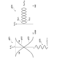
- FIG. 2 is a diagram showing the relationship between the ambient temperature of the laser and the oscillation wavelength.
- the horizontal axis of FIG. 2 is the temperature (degrees), and the vertical axis is the oscillation wavelength ( ⁇ m).
- the oscillation wavelength As shown in FIG. 2, when the ambient temperature of the laser changes, the oscillation wavelength also changes. For example, as the ambient temperature of the laser rises, the oscillation wavelength increases.
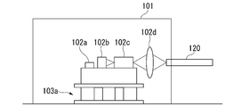
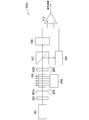
- FIG. 3 is a diagram showing a configuration example of the laser light source 101 according to the first embodiment.
- the laser light source 101 shown in FIG. 3 includes a thermistor 102a, a PD (photodetector) 102b, an LD (laser diode) chip 102c, a lens 102d, and a Peltier element 103a.
- the thermistor 102a measures, for example, the temperature of the substrate on which the PD 102b and the LD chip 102c are attached.
- the PD 102b measures the intensity of light emitted by the LD chip 102c and outputs the measured value to a laser driving unit (not shown).
- a laser drive unit controls the light intensity emitted from the LD chip 102c to a predetermined value based on the measurement value output from the PD 102b.
- the LD chip 102c emits light under the control of a laser driving unit (not shown).
- the lens 102d collects the light beam emitted from the LD chip 102c.
- the lens 102d makes the condensed light beam enter the optical fiber 120.
- the LD chip 102c is provided on the Peltier element 103a. With this configuration, the wavelength of the semiconductor laser 102 can be adjusted by adjusting the temperature of the LD chip 102c.
- ⁇ f is the phase of the fast axis.
- ⁇ s is the phase of the slow axis.
- ⁇ f is the wavelength of the fast axis.
- ⁇ s is the wavelength of the slow axis.
- c is the speed of light in vacuum.
- cf is the phase velocity of the fast axis.
- c s is the phase velocity of the slow axis.
- ⁇ is the wavelength in vacuum.
- f is the frequency in vacuum.
- d is the thickness of the electro-optic crystal.
- ⁇ n is the refractive index difference between the fast axis and the slow axis.
- the fast axis is a vibration direction in which light rapidly propagates in a crystal having birefringence.
- the slow axis is the vibration direction in which light propagates slowly in a crystal having birefringence.
- c′ is the speed of light in the electro-optic crystal.
- ⁇ is the dielectric constant in vacuum.
- ⁇ 0 is the dielectric constant in the electro-optic crystal.
- ⁇ is the magnetic permeability in vacuum.
- ⁇ 0 is the magnetic permeability in the electro-optic crystal.
- the wavelength of the laser is changed by adjusting the temperature of the semiconductor laser 102 so that the output of the differential amplifier 112 falls within a predetermined range including 0V.
- the fluctuation of the light intensity can be canceled by the laser.
- the balance shift is reduced and the balance point is located at an appropriate position. Therefore, according to the first embodiment, as described with reference to FIG. 8 and FIG.
- the signal strength is increased, and the S/N is less deteriorated, and stable electric field measurement can be performed.
- the device since the wave plate is not rotated, the device can be made simpler and smaller than the conventional electric field sensor. As a result, according to the first embodiment, it is possible to remove the fluctuation of the laser light by simplifying the configuration as compared with the conventional electric field sensor without impairing the measurement stability.
- the temperature control unit 114 may change the wavelength of the semiconductor laser 102 also by using the information output by the thermistor 102a shown in FIG.
- an external resonance type laser may be used.
- the wavelength and the optical path length of the external resonance type laser may be controlled so that the DC component extracted from the differential amplifier 112 falls within a predetermined range.
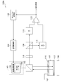
- FIG. 4 is a diagram showing a configuration example of the electric field sensor 100A according to the second embodiment.
- the electric field sensor 100A includes a laser light source 101, an electric field generation source 106, an electro-optic crystal 107, a polarization beam splitter 109, a light receiving circuit 110, a light receiving circuit 111, and a differential amplifier 112.
- the laser light source 101 includes a semiconductor laser 102 and a temperature controller 103.
- the constituent elements having the same functions as those of the electric field sensor 100 of the first embodiment are designated by the same reference numerals and the description thereof will be omitted.
- the polarization beam splitter 115 is arranged between the laser light source 101 and the first surface of the ITO 116.
- the ⁇ /4 wave plate 118 is arranged between the polarization beam splitter 115 and the polarization beam splitter 109.
- the electro-optic crystal 107 is in contact with the second surface of the ITO 116 and the first surface of the mirror 117.
- the polarization beam splitter 109 is arranged between the ⁇ /4 wave plate 118 and the light receiving circuit 110, and between the ⁇ /4 wave plate 118 and the light receiving circuit 111.
- the electric field sensor 100A obtains the amount of phase change induced by the electric field strength applied to the electro-optic crystal 107 mounted in the sensor by optical means.
- the electric field sensor 100A measures the output value of the differential amplifier 112 by a signal processing device (not shown) by applying the electric field generated by the measurement target from the mirror 117 side to the electro-optic crystal 107. The magnitude of the electric field generated by the measurement target is measured.
- the light beam emitted from the laser light source 101 passes through the polarization beam splitter 115, enters the ITO 116 as linearly polarized light, and then passes through the electro-optic crystal 107 and is reflected by the mirror 117.
- the reflected light beam passes through the electro-optic crystal 107 and the ITO 116, becomes an elliptically polarized light beam by the measurement electric field, and enters the polarization beam splitter 115 again.
- the incident light beam is reflected by the polarization beam splitter 115, is incident on the ⁇ /4 wavelength plate 118, is optically biased, and is incident on the polarization beam splitter 109.
- the polarization beam splitter 109 splits an elliptically polarized light beam into a P wave and an S wave.
- the ITO 116 is a transparent electrode and is grounded.
- the first surface of the mirror 117 is a mirror surface.
- the configuration shown in Fig. 4 is called a vertical electric field sensor. Even in such an electric field sensor having a vertical structure, when there is fluctuation (noise) in the light intensity due to the laser, the magnitude of the noise is proportional to the average power of light. Therefore, when the phase shifts due to the deviation of the optical components or the angular deviation of the wave plate, the differential balance shifts and the S/N deteriorates.
- the differential balance is adjusted in real time by controlling the output of the differential amplifier 112 to fall within a predetermined range including 0V.
- the signal intensity becomes larger than that when there is noise, and the S/N is deteriorated compared to when there is noise. Can be reduced.
- the means for changing the laser wavelength is not limited to the above-mentioned means.
- the temperature control unit 114 may change the wavelength of the semiconductor laser 102 by using the information output by the thermistor 102a shown in FIG.
- an external resonance type laser may be used.
- the wavelength and the optical path length of the external resonance type laser may be controlled so that the DC component extracted from the differential amplifier 112 falls within a predetermined range.
- the differential balance is electrically adjusted to 0 V by using the variable gain amplifier provided in the subsequent stage of the light receiving circuit.
- the differential wavelength is adjusted in real time by further changing the wavelength of the laser.
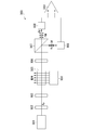
- FIG. 5 is a figure which shows the structural example of the electric field sensor 100B which concerns on 3rd Embodiment.
- the electric field sensor 100B includes a laser light source 101, an analyzer 104, a ⁇ /4 wavelength plate 105, an electric field generation source 106, an electro-optic crystal 107, and a ⁇ /2 wavelength plate 108.
- the polarization beam splitter 109, a light receiving circuit 110, a light receiving circuit 111, a differential amplifier 112, a DC level measuring unit 113, a temperature control unit 114B, a variable gain amplifier 121, and a variable gain amplifier 122 are provided.
- the laser light source 101 includes a semiconductor laser 102 and a temperature controller 103.
- the constituent elements having the same functions as those of the electric field sensor 100 of the first embodiment are designated by the same reference numerals and the description thereof will be omitted.
- the ⁇ /4 wave plate 105 optically biases the light incident on the electro-optic crystal 107, as in the first embodiment.
- the arrangement of optical components of the electric field sensor 100B is the same as that of the electric field sensor 100.
- the electric field sensor 100B applies an electric field generated by the object to be measured to the electro-optic crystal 107 to measure the output value of the differential amplifier 112 by a signal processing device (not shown). The magnitude of the electric field generated by the measurement target is measured.
- the output terminal of the light receiving circuit 110 is connected to the input terminal of the variable gain amplifier 121.
- the output terminal of the variable gain amplifier 121 is connected to the first input terminal of the differential amplifier 112.
- the control terminal of the variable gain amplifier 121 is connected to the temperature control unit 114B.
- the output terminal of the light receiving circuit 111 is connected to the input terminal of the variable gain amplifier 122.
- the output terminal of the variable gain amplifier 122 is connected to the second input terminal of the differential amplifier 112.
- the control terminal of the variable gain amplifier 122 is connected to the temperature control unit 114B.
- the output terminal of the differential amplifier 112 outputs the processed signal to a signal processing device (not shown).
- the temperature control unit 114B controls the gain variable amplifier so that the output of the differential amplifier 112 is in the second predetermined range including 0V in a state where the laser light source 101 emits light and the electric field generation source 106 does not generate an electric field.
- the gains of the variable gain amplifier 121 and the variable gain amplifier 122 are adjusted to electrically adjust them.
- the temperature control unit 114B causes the output of the differential amplifier 112 to fall within a predetermined range including 0 V with the laser light source 101 emitting light and the electric field generation source 106 generating an electric field. Therefore, the temperature controller 103 is controlled to optically adjust the temperature.
- the differential balance can be adjusted even if the photodetector sensitivity of the photodetectors included in each of the two photodetector circuits varies.
- the adjustment of the differential balance generated in the light receiving circuit is not limited to the variable gain amplifier described above.
- a first optical attenuator (not shown) may be provided between the polarizing beam splitter 109 and the light receiving circuit 110, and a second optical attenuator (not shown) may be provided between the polarizing beam splitter 109 and the light receiving circuit 111. ..
- the temperature control unit 114B causes the output of the differential amplifier 112 to fall within the second predetermined range including 0V in a state where the laser light source 101 emits light and the electric field generation source 106 does not generate an electric field. You may make it optically adjust by adjusting the attenuation factor of each of a 1st optical attenuator and a 2nd optical attenuator.
- the means for changing the laser wavelength is not limited to the above-mentioned means.
- the temperature control unit 114B may change the wavelength of the semiconductor laser 102 also by using the information output by the thermistor 102a shown in FIG.
- an external resonance type laser may be used. In this case, the wavelength and the optical path length of the external resonance type laser may be controlled so that the DC component extracted from the differential amplifier 112 falls within a predetermined range.
- FIG. 6 is a diagram showing a configuration example of an electric field sensor 100C according to the fourth embodiment.
- the electric field sensor 100C includes a laser light source 101, an electric field generation source 106, an electro-optic crystal 107, a polarization beam splitter 109, a light receiving circuit 110, a light receiving circuit 111, and a differential amplifier 112.
- the laser light source 101 includes a semiconductor laser 102 and a temperature controller 103.
- the components having the same functions as those of the electric field sensor 100 according to the first embodiment, the electric field sensor 100A according to the second embodiment, and the electric field sensor 100B according to the third embodiment are denoted by the same reference numerals and description thereof will be omitted.
- the ⁇ /4 wave plate 118 optically biases the light incident on the polarization beam splitter 115.
- the electric field sensor 100C applies the electric field generated by the object to be measured from the mirror 117 side to the electro-optic crystal 107, so that the output value of the differential amplifier 112 is not shown in the signal processing device. By measuring with, the magnitude of the electric field generated by the measurement target is measured.
- the temperature control unit 114B outputs 0 V as the output of the differential amplifier 112 when the laser light source 101 emits light and the electric field generation source 106 does not generate an electric field.
- the gains of the variable gain amplifier 121 and the variable gain amplifier 122 are electrically adjusted by adjusting the gains of the variable gain amplifier 121 and the variable gain amplifier 122 so as to fall within the second predetermined range.
- the temperature control unit 114B controls the temperature controller 103 so that the output of the differential amplifier 112 is within a predetermined range including 0 V in a state where the laser light source 101 emits light and the electric field generation source 106 generates an electric field. Optically adjusted by controlling.
- the differential balance can be adjusted even if the photodetectors of the two photodetectors have variations in the photosensitivity.
- the adjustment of the differential balance occurring in the light receiving circuit is not limited to the above-described variable gain amplifier.
- a first optical attenuator (not shown) may be provided between the polarizing beam splitter 109 and the light receiving circuit 110, and a second optical attenuator (not shown) may be provided between the polarizing beam splitter 109 and the light receiving circuit 111. ..
- the temperature control unit 114B causes the output of the differential amplifier 112 to fall within the second predetermined range including 0V in a state where the laser light source 101 emits light and the electric field generation source 106 does not generate an electric field. You may make it optically adjust by adjusting the attenuation factor of each of a 1st optical attenuator and a 2nd optical attenuator.
- the means for changing the laser wavelength is not limited to the above-mentioned means.
- the temperature control unit 114B may change the wavelength of the semiconductor laser 102 also by using the information output by the thermistor 102a shown in FIG.
- an external resonance type laser may be used. In this case, the wavelength and the optical path length of the external resonance type laser may be controlled so that the DC component extracted from the differential amplifier 112 falls within a predetermined range.
- 100, 100A, 100B, 100C... Electric field sensor 101... Laser light source, 102... Semiconductor laser, 103... Temperature controller, 104... Analyzer, 105... ⁇ /4 wavelength plate, 106... Electric field generation source, 107... Electro-optics Crystal, 108... ⁇ /2 wavelength plate, 109... Polarization beam splitter, 110... Photodetector circuit, 111... Photodetector circuit, 112... Differential amplifier, 113... DC level measuring section, 114, 114B... Temperature control section, 115... Polarization Beam splitter, 116... ITO, 117... Mirror, 118... ⁇ /4 wavelength plate, 121... Gain variable amplifier, 122... Gain variable amplifier
Landscapes
- Physics & Mathematics (AREA)
- General Physics & Mathematics (AREA)
- Electromagnetism (AREA)
- Measuring Instrument Details And Bridges, And Automatic Balancing Devices (AREA)
- Optical Modulation, Optical Deflection, Nonlinear Optics, Optical Demodulation, Optical Logic Elements (AREA)
Abstract
電界センサは、光源と、光源が出射した光に基づく所定の偏光状態の光が入射され、被対象物が発する電界を受ける電気光学結晶と、電気光学結晶から出射される光をP波とS波とに分離する第1分離部と、第1分離部の前段で、光の位相を変化させる第1波長板と、P波の光を受光し、受光した光を第1電気信号に変換する第1受光部と、S波の光を受光し、受光した光を第2電気信号に変換する第2受光部と、第1受光部が変換した第1電気信号と、第2受光部が変換した第2電気信号との差動信号を生成する差動増幅部と、光源から光が出射され電気光学結晶に電界を印加した状態の差動増幅部の直流成分の出力値を所定の値の範囲になるように、光源の波長を調整する制御部と、を備える。
Description
本発明は、電界センサに関する。
本願は、2019年1月22日に、日本に出願された特願2019-008252号に基づき優先権を主張し、その内容をここに援用する。
本願は、2019年1月22日に、日本に出願された特願2019-008252号に基づき優先権を主張し、その内容をここに援用する。
電界を測定する電界センサとしては、センサエレメントが一般的なダイポールアンテナのような金属製のものが一般的である。
これに対して、電気光学効果を用いた電界測定は、センサエレメントが金属製ではないため測定対象の電界を乱さずに測ることができ、さらに高空間分解の測定が可能である。このため、電気光学効果を用いた電界測定は、色々な用途で使われ始めている。なお、電気光学効果とは、電気光学結晶に電界が印加されると、電界強度に応じて電気光学結晶を透過する光の屈折率が変化する効果である。また、屈折率の変化は、光学結晶を通過する光波の位相変化を与える。電気光学効果を用いた電界測定では、位相の変化を測定することで、電気光学結晶に印加されている電界を測定することができる(例えば、特許文献1、2参照)。
これに対して、電気光学効果を用いた電界測定は、センサエレメントが金属製ではないため測定対象の電界を乱さずに測ることができ、さらに高空間分解の測定が可能である。このため、電気光学効果を用いた電界測定は、色々な用途で使われ始めている。なお、電気光学効果とは、電気光学結晶に電界が印加されると、電界強度に応じて電気光学結晶を透過する光の屈折率が変化する効果である。また、屈折率の変化は、光学結晶を通過する光波の位相変化を与える。電気光学効果を用いた電界測定では、位相の変化を測定することで、電気光学結晶に印加されている電界を測定することができる(例えば、特許文献1、2参照)。
ここで、電気光学効果を利用した電界センサの構成例と動作例を説明する。
図7は、従来技術に係る電気光学効果を利用した電界センサ900の構成例と動作例を示す図である。図7に示すように、電界センサ900は、レーザ光源901と、検光子902と、λ/4波長板903と、電界発生源904と、電気光学結晶905と、λ/2波長板906と、偏光ビームスプリッタ907と、フォトディテクタ908と、フォトディテクタ909と、差動増幅器910を有している。
図7は、従来技術に係る電気光学効果を利用した電界センサ900の構成例と動作例を示す図である。図7に示すように、電界センサ900は、レーザ光源901と、検光子902と、λ/4波長板903と、電界発生源904と、電気光学結晶905と、λ/2波長板906と、偏光ビームスプリッタ907と、フォトディテクタ908と、フォトディテクタ909と、差動増幅器910を有している。
レーザ光源901は、例えば半導体レーザである。検光子902は、レーザ光源901から入射した光線のうち直線偏光を出射する。λ/4波長板903は、検光子902から入射した光線を円偏光に偏光して出射する。
電界発生源904は、電気光学結晶905に対して電界を発生させる。電気光学結晶905は、電界発生源904によって印加される電界強度に応じた複屈折の変化により偏光状態を変化させる。電気光学結晶905は、楕円軸の方位が45度に傾いた楕円偏光の光線を出射する。なお、楕円偏光の楕円率は、電界の強度によって変化する。λ/2波長板906は、電気光学結晶905が出射した光線を楕円偏光の楕円率を保ったまま、楕円偏光の方位が0度となる楕円偏光に変える。
偏光ビームスプリッタ907は、λ/2波長板906が出射した楕円偏光の方位が0度である楕円偏光の光線をP波とS波に分離する。フォトディテクタ908は、偏光ビームスプリッタ907から入射したP波を電気信号に変換し、変換したP波成分の電気信号を差動増幅器910の一方の入力端に出力する。フォトディテクタ909は、偏光ビームスプリッタ907から入射したS波を電気信号に変換し、変換したS波成分の電気信号を差動増幅器910の他方の入力端に出力する。
差動増幅器910は、P波成分とS波成分の電気信号の差動成分を増幅して、増幅した電気信号を不図示の信号処理装置に出力する。なお、P波とS波の強度の時間変化は逆位相となるため、電界強度信号は、差動増幅器910によって2倍となる。
ここで、検光子902を透過後の光強度をIOとし、P波の光強度をIPとし、S波の光強度をISとすると、P波の透過率TPは位相差Γを用いて次式(1)で表される。また、S波の透過率TSは位相差Γを用いて次式(2)で表される。


ここで、電気光学結晶905に印加される電圧が正弦波であり、位相差(Γ(t)=a・sin(2πft))が時間的に変動する場合、P波の透過率TP(t)は次式(3)のように表される。また、S波の透過率TS(t)は次式(4)のように表される。


ここで、P波の透過率TP(t)とS波の透過率TS(t)の差動バランスがあっている場合は、P波の平均光パワーTPOとS波の平均光パワーTSOが等しいため、図8のように動作する。図8は、P波の透過率TP(t)とS波の透過率TS(t)の差動バランスがあっている場合の動作を説明するための図である。図8の符号g921が示すグラフにおいて、横軸は位相差Γであり、縦軸は透過率Tである。また、符号g922はP波による変化を表している。また、符号g923はS波による変化を表している。符号g924のグラフは、平均位相差0におけるP波とS波の光強度の変化を表している。符号g925は、平均位相差0における位相差の変化を表している。
これに対して、レーザ光に強度揺らぎ(雑音)がある場合、理想的にはP波の透過率TP(t)とS波の透過率TS(t)の波形に同相で重畳するため、その雑音の大きさはP波の平均光パワーTPOとS波の平均光パワーPSOに比例する。差動バランスがあっている場合は、TPO=TSOとなるため、差動増幅器910によって雑音成分をキャンセルすることができる。
しかしながら、現実的には電気光学結晶905を含む光学部品の旋光性や偏差や波長板の角度偏差等により、図9のように位相がずれてくる。図9は、P波の透過率TP(t)とS波の透過率TS(t)の差動バランスがずれている場合の動作を説明するための図である。図9の符号g931が示すグラフにおいて、横軸は位相差Γであり、縦軸は透過率Tである。また、符号g932はP波による変化を表している。また、符号g933はS波による変化を表している。符号g934のグラフは、位相差にオフセットΓ0が加わったP波とS波の光強度の変化を表している。符号g935は、位相差にオフセットΓ0が加わった位相差の変化を表している。
しかしながら、現実的には電気光学結晶905を含む光学部品の旋光性や偏差や波長板の角度偏差等により、図9のように位相がずれてくる。図9は、P波の透過率TP(t)とS波の透過率TS(t)の差動バランスがずれている場合の動作を説明するための図である。図9の符号g931が示すグラフにおいて、横軸は位相差Γであり、縦軸は透過率Tである。また、符号g932はP波による変化を表している。また、符号g933はS波による変化を表している。符号g934のグラフは、位相差にオフセットΓ0が加わったP波とS波の光強度の変化を表している。符号g935は、位相差にオフセットΓ0が加わった位相差の変化を表している。
差動バランスがずれている場合は、次式(5)と次式(6)のように、位相差にオフセットΓ0が生じ、差動バランスがずれる。


レーザ光に強度揺らぎ(雑音)がある場合、P波の透過率TP(t)とS波の透過率TS(t)の波形に同相で重畳するため、上述したように雑音の大きさは平均パワーTPOとTSOに比例する。ここで、差動バランスがずれている場合は、TPOとTSOが等しくならず、雑音の大きさが異なる。このため、差動増幅器910によってキャンセルできない。また、図9の符号g934のグラフに示したように、バランス点からずれると変調効率が小さい点にバイアスされるので、信号成分が減少する。このように、P波とS波のバランスが崩れた場合は、S/Nが劣化する。
このため、従来、組み立て調整で、図10に示すように、波長板を回転させることでバランスを調整することが行われている。図10は、波長板を回転させて差動バランスを調整する構成例を示す図である。図10において、図7と同じ機能の部品には同じ符号を用いて説明を省略する。
図10に示したように、電界センサ900aは、レーザ光源901と、検光子902と、λ/4波長板903aと、電界発生源904と、電気光学結晶905と、λ/2波長板906bと、偏光ビームスプリッタ907と、フォトディテクタ908と、フォトディテクタ909と、差動増幅器910を有している。
電気光学結晶905に電界が印加されていないときにおいても、光学的なバランス点のずれにより、フォトディテクタ908とフォトディテクタ909の両方の出力に差が生じて、差動増幅器910の出力が0にならない。このため、電界センサ900aでは、λ/4波長板903aとλ/2波長板906bを回転させてP波とS波のバランスを光学的に調整する。
電気光学結晶905に電界が印加されていないときにおいても、光学的なバランス点のずれにより、フォトディテクタ908とフォトディテクタ909の両方の出力に差が生じて、差動増幅器910の出力が0にならない。このため、電界センサ900aでは、λ/4波長板903aとλ/2波長板906bを回転させてP波とS波のバランスを光学的に調整する。
しかしながら、図10に示したようにλ/4波長板903aとλ/2波長板906bを回転させてP波とS波のバランスを光学的に調整した場合は、レーザ光の揺らぎを除去できるが、構成が複雑になり装置も大型になる場合がある。
本発明の一態様は、上記事情に鑑みてなされたものであって、電気光学効果を利用した電界センサにおいて、従来の電界センサより構成を簡素化してレーザ光の揺らぎを除去することができる電界センサを提供することを目的とする。
上記目的を達成するため、本発明の一態様に係る電界センサ(電界センサ100,100A,100B,100C)は、光源(半導体レーザ102)と、前記光源が出射した光に基づく所定の偏光状態の光が入射され、前記被対象物が発する電界を受ける電気光学結晶(電気光学結晶107)と、前記電気光学結晶から出射される光をP波とS波とに分離する第1分離部(偏光ビームスプリッタ109)と、前記第1分離部の前段で、光の位相を変化させる第1波長板(λ/4波長板105)と、前記P波の光を受光し、受光した光を第1電気信号に変換する第1受光部(受光回路110)と、前記S波の光を受光し、受光した光を第2電気信号に変換する第2受光部(受光回路111)と、前記第1受光部が変換した前記第1電気信号と、前記第2受光部が変換した前記第2電気信号との差動信号を生成する差動増幅部(差動増幅器112)と、前記光源から光が出射され前記電気光学結晶に電界を印加した状態の前記差動増幅部の直流成分の出力値を所定の値の範囲になるように、前記光源の波長を調整する制御部(DCレベル測定部113、温度制御部114、温度調節器103)と、を備える。
上記の構成により、電界センサは、差動増幅部の出力が所定の範囲になるように光源の温度を調整することでレーザの波長を変更する。これにより、上記構成によれば、レーザにより光強度の揺らぎ(雑音)をキャンセルすることができる。この結果、バランスずれが減少し、バランス点が適切な位置となる。そのため、上記構成によれば、バランスがずれている場合と比較して信号強度が上がり、S/Nの劣化が少なく安定した電界測定を行うことができる。また、上記構成では、波長板を回転させないため、装置を従来の電界センサより簡素化でき小型化することができる。これにより、上記構成によれば、測定安定度を損なうことなく、従来の電界センサより構成を簡素化してレーザ光の揺らぎを除去することができる。
また、本発明の一態様に係る測定装置において、前記制御部は、前記光源から光が出射され前記電気光学結晶に電界を印加した状態の前記差動増幅部の直流成分の出力値を前記所定の値の範囲になるように、前記光源の温度を調整することで前記光源の波長を調整するようにしてもよい。
上記の構成により、電界センサは、電気光学結晶に電界が印加されている状態の光学部品によるばらつきを制御部で調整するようにした。これにより、上記構成によれば、レーザにより光強度の揺らぎ(雑音)をよりキャンセルすることができる。この結果、バランスずれが減少し、バランス点が適切な位置となるため、上記構成によれば、バランスがずれている場合と比較して信号強度が上がり、S/Nの劣化が少なく安定した電界測定を行うことができる。
また、本発明の一態様に係る測定装置は、透明電極(ITO116)と、ミラー(ミラー117)と、をさらに備え、前記電気光学結晶は、一方の面に前記透明電極が対向して配置され、他方の面に前記ミラーが配置され、前記光源が出射した光に基づく所定の偏光状態の光が前記透明電極から入射され、前記透明電極から入射した光を前記ミラーによって反射し、反射した光を前記透明電極から出射し、前記透明電極から出射された光が前記分離部に入射するようにしてもよい。
上記の構成により、電界センサは、構造が縦型であっても、レーザにより光強度の揺らぎ(雑音)をよりキャンセルすることができる。この結果、バランスずれが減少し、バランス点が適切な位置となるため、上記構成によれば、バランスがずれている場合と比較して信号強度が上がり、S/Nの劣化が少なく安定した電界測定を行うことができる。
また、本発明の一態様に係る測定装置は、前記第1受光部の前記第1電気信号の第1利得を変更する第1利得可変部(利得可変増幅器121)と、前記第2受光部の前記第2電気信号の第2利得を変更する第2利得可変部(利得可変増幅器122)と、をさらに備え、前記制御部は、前記光源から光が出射され前記電気光学結晶に電界が印加されていない状態の前記差動増幅部の直流成分の出力値を所定の値の範囲になるように、前記第1利得可変部の前記第1利得と前記第2利得可変部の前記第2利得を調整するようにしてもよい。
上記の構成により、電界センサは、電気光学結晶に電界が印加されていない状態の光学部品によるばらつきを第1利得可変部と第2利得可変部で調整し、電気光学結晶に電界が印加されている状態の光学部品によるばらつきを制御部で調整するようにした。これにより、上記構成によれば、レーザにより光強度の揺らぎ(雑音)をよりキャンセルすることができる。この結果、バランスずれが減少し、バランス点が適切な位置となるため、上記構成によれば、バランスがずれている場合と比較して信号強度が上がり、S/Nの劣化が少なく安定した電界測定を行うことができる。
また、本発明の一態様に係る電界センサ(電界センサ100,100A,100B,100C)は、電気光学効果を利用して、前記被対象物が発する電界を測定するようにしてもよい。
また、本発明の一態様に係る前記第1波長板(λ/4波長板105)は、前記第1波長板の光軸の方位が、所定の軸に対して、第1角度傾けて配置されてもよい。
また、本発明の一態様に係る前記第1波長板(λ/4波長板105)は、前記電気光学結晶(電気光学結晶107)の前段に配置され、前記電界センサ(電界センサ100,100B)は、前記電気光学結晶の後段に配置され、前記第1分離部の後段で、光の位相を変化させる第2波長板(λ/2波長板108)をさらに備えてもよい。
また、本発明の一態様に係る前記第2波長板(λ/2波長板108)は、前記第2波長板の光軸の方位が、前記所定の軸に対して、第2角度傾けて配置されてもよい。
また、本発明の一態様に係る前記光源(レーザ光源101)は、発光するレーザダイオードチップ(LDチップ102c)と、前記レーザダイオードチップが発光した光の光強度を測定するフォトディテクタ(PD102b)と、前記レーザダイオードチップと前記フォトディテクタが取り付けられる基板の温度を測定するサーミスタ(サーミスタ102a)と、前記レーザダイオードチップが出射する光線を集光するレンズ(レンズ102d)と、を備えてもよい。
また、本発明の一態様に係る電界センサ(電界センサ100A,100C)は、前記光源(レーザ光源101)と、前記透明電極(ITO116)の前記一方の面との間に配置される第2分離部(偏光ビームスプリッタ115)を更に備えてもよい。
また、本発明の一態様に係る前記制御部(DCレベル測定部113、温度制御部114、温度調節器103)は、前記第1利得可変部の利得と前記第2利得可変部の利得を、リアルタイムで調整してもよい。
また、本発明の一態様に係る前記制御部(DCレベル測定部113、温度制御部114、温度調節器103)は、前記光源から光が出射され前記電気光学結晶(電気光学結晶107)に電界を印加した状態の前記差動増幅部(差動増幅器112)の直流成分の出力値と、前記サーミスタ(サーミスタ102a)が出力する情報と、を用いて、前記光源(レーザ光源101)の温度を調整することで前記光源の波長を調整してもよい。
また、本発明の一態様に係る前記光源(レーザ光源101)は、外部共振型レーザを備えてもよい。
また、本発明の一態様に係る電界センサ(100B,100C)は、前記第1分離部と前記第1受光部との間に設けられる第1光アッテネータと、前記第1分離部と前記第2受光部との間に設けられる第2光アッテネータと、をさらに備え、前記制御部(DCレベル測定部113、温度制御部114、温度調節器103)は、前記光源を発光させ被対象物によって電界を発生させていない状態で、前記差動増幅部の出力が所定の範囲になるように、前記第1の光アッテネータと前記第2の光アッテネータそれぞれの減衰率を調整してもよい。
本発明の一態様によれば、従来の電界センサより構成を簡素化してレーザ光の揺らぎを除去することができる。
以下、本発明の第1~第4実施形態について図面を参照しながら説明する。なお、以下の説明に用いる図面では、各部材を認識可能な大きさとするため、各部材の縮尺を適宜変更している。
<第1実施形態>
図1は、第1実施形態に係る電界センサ100の構成例を示す図である。図1に示すように、電界センサ100は、レーザ光源101(光源)と、検光子104と、λ/4波長板105(第1波長板)と、電界発生源106と、電気光学結晶107と、λ/2波長板108(第2波長板)と、偏光ビームスプリッタ109(第1分離部)と、受光回路110(第1受光部)と、受光回路111(第2受光部)と、差動増幅器112(差動増幅部)と、DCレベル測定部113(制御部)と、温度制御部114(制御部)を備えている。また、レーザ光源101は、半導体レーザ102(光源)と、温度調節器103(制御部)を備えている。なお、符号g111に示すように、図1において、レーザ光源101から出射された光は進行方向に振動成分を持たない横波であり、進行方向に対し磁界振動方向をx軸とし、電界振動方向をy軸とする。
図1は、第1実施形態に係る電界センサ100の構成例を示す図である。図1に示すように、電界センサ100は、レーザ光源101(光源)と、検光子104と、λ/4波長板105(第1波長板)と、電界発生源106と、電気光学結晶107と、λ/2波長板108(第2波長板)と、偏光ビームスプリッタ109(第1分離部)と、受光回路110(第1受光部)と、受光回路111(第2受光部)と、差動増幅器112(差動増幅部)と、DCレベル測定部113(制御部)と、温度制御部114(制御部)を備えている。また、レーザ光源101は、半導体レーザ102(光源)と、温度調節器103(制御部)を備えている。なお、符号g111に示すように、図1において、レーザ光源101から出射された光は進行方向に振動成分を持たない横波であり、進行方向に対し磁界振動方向をx軸とし、電界振動方向をy軸とする。
まず、電界センサ100の光学的な構成要素の配置を説明する。
検光子104は、レーザ光源101とλ/4波長板105との間に配置される。λ/4波長板105は、検光子104と電気光学結晶107との間に配置される。電気光学結晶107は、λ/4波長板105とλ/2波長板108との間に配置される。λ/2波長板108は、電気光学結晶107と偏光ビームスプリッタ109との間に配置される。偏光ビームスプリッタ109は、λ/2波長板108と受光回路110との間、かつλ/2波長板108と受光回路111との間に配置される。
検光子104は、レーザ光源101とλ/4波長板105との間に配置される。λ/4波長板105は、検光子104と電気光学結晶107との間に配置される。電気光学結晶107は、λ/4波長板105とλ/2波長板108との間に配置される。λ/2波長板108は、電気光学結晶107と偏光ビームスプリッタ109との間に配置される。偏光ビームスプリッタ109は、λ/2波長板108と受光回路110との間、かつλ/2波長板108と受光回路111との間に配置される。
次に、電界センサ100の電気的な構成要素の接続関係を説明する。
受光回路110の出力端は、差動増幅器112の第1入力端子に接続されている。受光回路111の出力端は、差動増幅器112の第2入力端子に接続されている。差動増幅器112の出力端は、不図示の信号処理装置に処理した信号を出力する。
受光回路110の出力端は、差動増幅器112の第1入力端子に接続されている。受光回路111の出力端は、差動増幅器112の第2入力端子に接続されている。差動増幅器112の出力端は、不図示の信号処理装置に処理した信号を出力する。
次に、電界センサ100の動作について説明する。
電界センサ100は、センサ内に実装している電気光学結晶107に印加される電界強度に誘起される位相変化量を光学的手段で得ている。なお、電界センサ100は、被測定対象が発生する電界を電気光学結晶107に与えることで、差動増幅器112の出力値を不図示の信号処理装置によって測定することで、被測定対象が発生する電界の大きさを測定する。
電界センサ100は、センサ内に実装している電気光学結晶107に印加される電界強度に誘起される位相変化量を光学的手段で得ている。なお、電界センサ100は、被測定対象が発生する電界を電気光学結晶107に与えることで、差動増幅器112の出力値を不図示の信号処理装置によって測定することで、被測定対象が発生する電界の大きさを測定する。
半導体レーザ102は、例えば半導体レーザである。半導体レーザ102は、不図示のレーザ駆動部によって駆動され発光する。
温度調節器103は、半導体レーザ102に取り付けられている。温度調節器103は、例えばペルチェ素子である。温度調節器103は、温度制御部114の制御に応じて半導体レーザ102の温度を調整する。
温度調節器103は、半導体レーザ102に取り付けられている。温度調節器103は、例えばペルチェ素子である。温度調節器103は、温度制御部114の制御に応じて半導体レーザ102の温度を調整する。
検光子104は、レーザ光源101から入射した光線のうち直線偏光(符号g101、g111)を出射する。
λ/4波長板105は、光軸の方位をx軸に対して45度傾けて配置されている。λ/4波長板105は、検光子104から入射した光線を円偏光(符号g102、g112)に偏光して出射する。換言すると、λ/4波長板105は、電気光学結晶107に入射する光に対して光学的にバイアスをかけている。
λ/4波長板105は、光軸の方位をx軸に対して45度傾けて配置されている。λ/4波長板105は、検光子104から入射した光線を円偏光(符号g102、g112)に偏光して出射する。換言すると、λ/4波長板105は、電気光学結晶107に入射する光に対して光学的にバイアスをかけている。
電界発生源106は、電気光学結晶107に対して電界を発生させる。
電気光学結晶107は、電界発生源106によって印加される電界強度に応じた複屈折の変化により偏光状態を変化させる。電気光学結晶107は、楕円軸の方位が45度に傾いた楕円偏光(符号g103、g113)の光線を出射する。なお、楕円偏光の楕円率は、電界の強度によって変化する。電気光学結晶107は、例えばLiNbO3、LiTaO3、Bi12SiO20(BSO)、Bi12GeO20(BGO)、ADP、KDP等である。
電気光学結晶107は、電界発生源106によって印加される電界強度に応じた複屈折の変化により偏光状態を変化させる。電気光学結晶107は、楕円軸の方位が45度に傾いた楕円偏光(符号g103、g113)の光線を出射する。なお、楕円偏光の楕円率は、電界の強度によって変化する。電気光学結晶107は、例えばLiNbO3、LiTaO3、Bi12SiO20(BSO)、Bi12GeO20(BGO)、ADP、KDP等である。
λ/2波長板108は、光軸の方位をx軸に対して22.5度傾けて配置されている。λ/2波長板108は、電気光学結晶107が出射した光線を楕円偏光の楕円率を保ったまま、楕円偏光の方位が0度となる楕円偏光(符号g104、g114)に変える。
偏光ビームスプリッタ109は、λ/2波長板108が出射した楕円偏光の方位が0度である楕円偏光の光線をP波(符号g105、g115)とS波(符号g106、g116)に分離する。
受光回路110は、フォトディテクタを有する。受光回路110は、偏光ビームスプリッタ109から入射したP波を電気信号に変換し、変換したP波成分の電気信号を差動増幅器112の第1入力端子に出力する。
受光回路111は、フォトディテクタを有する。受光回路111は、偏光ビームスプリッタ109から入射したS波を電気信号に変換し、変換したS波成分電気信号を差動増幅器112の第2入力端に出力する。
差動増幅器112は、P波成分とS波成分の電気信号の差動成分を増幅して、増幅した電気信号を不図示の信号処理装置に出力する。
DCレベル測定部113は、差動増幅器112が出力するDC(直流)のレベルを測定し、測定したDCレベルを示す値または情報を温度制御部114に出力する。
温度制御部114は、DCレベル測定部113が出力するDCレベルを示す値または情報を取得する。温度制御部114は、DCレベルを示す値が0Vを含む所定の値の範囲に入るように温度調節器103を制御する。
温度制御部114は、DCレベル測定部113が出力するDCレベルを示す値または情報を取得する。温度制御部114は、DCレベルを示す値が0Vを含む所定の値の範囲に入るように温度調節器103を制御する。
第1実施形態では、差動増幅器112の出力からDCレベル測定部113によって直流成分を取り出し、取り出した直流成分が0Vを含む所定の範囲に入るように半導体レーザ102の温度を温度制御部114と温度調節器103によって制御する。なお、温度制御部114と温度調節器103は、半導体レーザ102の温度の調整をリアルタイムで行う。
ここで、レーザの周囲温度と発振波長の関係を説明する。
図2は、レーザの周囲温度と発振波長の関係を示す図である。図2の横軸は温度(度)であり、縦軸は発振波長(μm)である。図2に示したように、レーザの周囲温度が変化すると、発振波長も変化する。例えば、レーザの周囲温度が上昇すると、発振波長は大きくなる。
図2は、レーザの周囲温度と発振波長の関係を示す図である。図2の横軸は温度(度)であり、縦軸は発振波長(μm)である。図2に示したように、レーザの周囲温度が変化すると、発振波長も変化する。例えば、レーザの周囲温度が上昇すると、発振波長は大きくなる。
次に、レーザ光源101の構成例を説明する。
図3は、第1実施形態に係るレーザ光源101の構成例を示す図である。図3に示すレーザ光源101は、サーミスタ102aと、PD(フォトディテクタ)102bと、LD(レーザダイオード)チップ102cと、レンズ102dと、ペルチェ素子103aを含んでいる。
図3は、第1実施形態に係るレーザ光源101の構成例を示す図である。図3に示すレーザ光源101は、サーミスタ102aと、PD(フォトディテクタ)102bと、LD(レーザダイオード)チップ102cと、レンズ102dと、ペルチェ素子103aを含んでいる。
サーミスタ102aは、例えばPD102bとLDチップ102cが取り付けられている基板の温度を測定する。
PD102bは、LDチップ102cによって発光された光強度を測定し、測定した測定値を不図示のレーザ駆動部に出力する。不図示のレーザ駆動部は、PD102bが出力する測定値に基づいてLDチップ102cが出射する光強度を所定値に制御する。
PD102bは、LDチップ102cによって発光された光強度を測定し、測定した測定値を不図示のレーザ駆動部に出力する。不図示のレーザ駆動部は、PD102bが出力する測定値に基づいてLDチップ102cが出射する光強度を所定値に制御する。
LDチップ102cは、不図示のレーザ駆動部の制御に応じて発光する。
レンズ102dは、LDチップ102cが出射した光線を集光する。レンズ102dは、集光された光線を光ファイバ120に入射する。
レンズ102dは、LDチップ102cが出射した光線を集光する。レンズ102dは、集光された光線を光ファイバ120に入射する。
図3に示す構造では、ペルチェ素子103a上にLDチップ102cが設けられている。この構成により、LDチップ102cの温度を調整することで、半導体レーザ102の波長を調整することができる。
ここで、レーザの波長を変更することで、複屈折を有する電気光学結晶中を伝搬する光の位相差を変更することができる原理について説明する。
複屈折を持つ電気光学結晶の通過後の光学的位相差Γ(λ)は、次式(7)のように表される。
複屈折を持つ電気光学結晶の通過後の光学的位相差Γ(λ)は、次式(7)のように表される。
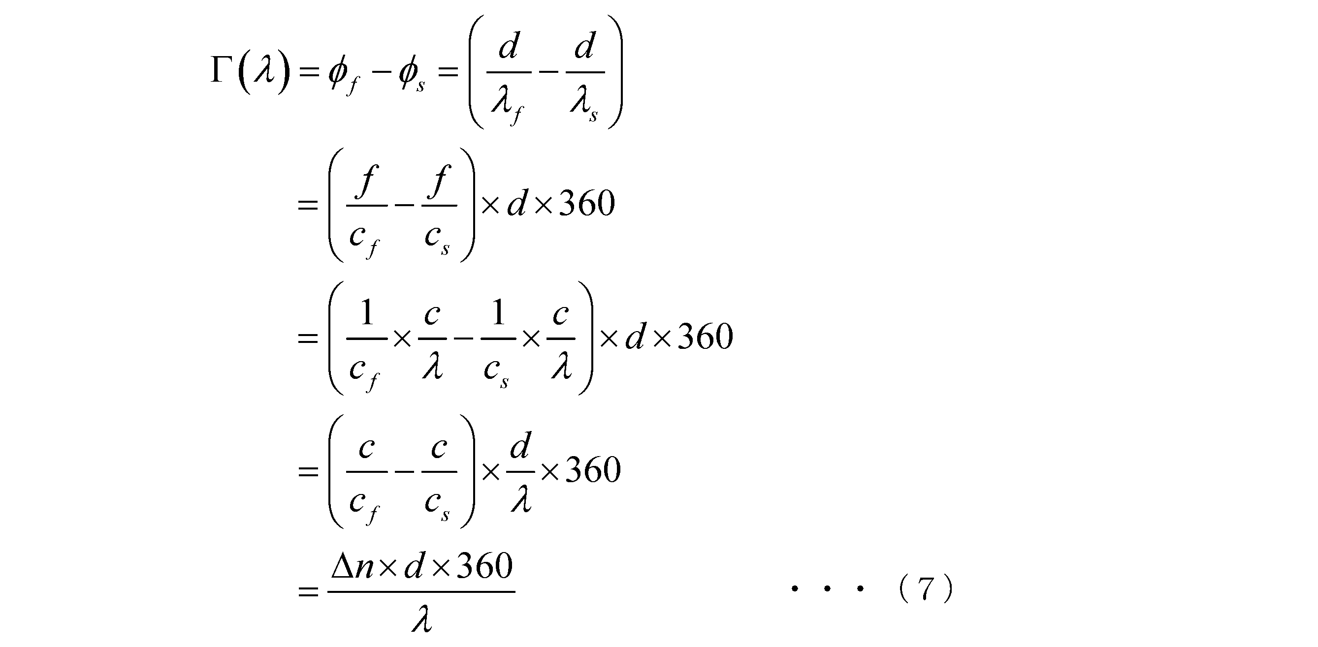
式(7)において、φfはfast軸の位相である。また、φsはslow軸の位相である。また、λfはfast軸の波長である。また、λsはslow軸の波長である。cは真空中の光速である。また、cfはfast軸の位相速度である。また、csはslow軸の位相速度である。λは真空中での波長である。また、fは真空中での周波数である。dは電気光学結晶の厚さである。Δnはfast軸とslow軸の屈折率差である。なお、fast軸とは複屈折を有する結晶中を光が速く伝搬する振動方向である。また、slow軸とは複屈折を有する結晶中を光が遅く伝搬する振動方向である。
式(7)に示したように、真空中で波長がλであり周波数がfである光が、厚さdの複屈折を持つ電気光学結晶中を伝搬するとき、fast軸の振動方向の光とslow軸の振動方向の光との位相差Γ(λ)は、波長λに対して反比例の関係である。
ここで、屈折率nは、次式(8)で表される。
ここで、屈折率nは、次式(8)で表される。

式(8)にいて、c’は電気光学結晶中の光速である。また、εは真空中の誘電率である。また、ε0は電気光学結晶中の誘電率である。また、μは真空中の透磁率である。また、μ0は電気光学結晶中の透磁率である。
式(7)より、fast軸とslow軸の屈折率差Δnは、次式(9)のようになる。

式(9)示したように、レーザの波長を変更することで、複屈折を有する電気光学結晶中を伝搬するfast軸の振動方向の光とslow軸の振動方向の光の位相差を変更することができる。これにより、図10を用いて説明した従来技術における波長板を回転させて光学的なバランスを調整することと同等の効果を得ることができる。
上述したように、光学的なバランス点のずれによって、受光回路110と受光回路111の両出力に差が生じて差動増幅器112の出力に偏差電圧が生じる。第1実施形態では、このような場合であっても、差動増幅器112の出力が0Vを含む所定の範囲になるように半導体レーザ102の温度を調整することでレーザの波長を変更する。これにより、第1実施形態によれば、レーザにより光強度の揺らぎ(雑音)をキャンセルすることができる。この結果、バランスずれが減少し、バランス点が適切な位置となるため、図8、図9を用いて説明したように、第1実施形態によれば、バランスがずれている場合と比較して信号強度が上がり、S/Nの劣化が少なく安定した電界測定を行うことができる。また、第1実施形態では、波長板を回転させないため、装置を従来の電界センサより簡素化でき小型化することができる。これにより、第1実施形態によれば、測定安定度を損なうことなく、従来の電界センサより構成を簡素化してレーザ光の揺らぎを除去することができる。
なお、レーザの波長を変更する手段は、上述した手段に限らない。温度制御部114は、図3に示したサーミスタ102aが出力する情報も用いて、半導体レーザ102の波長を変更してもよい。または、外部共振型レーザを用いてもよい。この場合は、差動増幅器112から取り出した直流成分が所定の範囲になるように、外部共振型レーザの波長と光路長を変更するように制御してもよい。
<第2実施形態>
第2実施形態では、電界センサが縦型構造の例を説明する。
図4は、第2実施形態に係る電界センサ100Aの構成例を示す図である。図4に示すように、電界センサ100Aは、レーザ光源101と、電界発生源106と、電気光学結晶107と、偏光ビームスプリッタ109と、受光回路110と、受光回路111と、差動増幅器112と、DCレベル測定部113と、温度制御部114と、偏光ビームスプリッタ115(第2分離部)と、ITO(Indium Tin Oxide)116と、ミラー117と、λ/4波長板118を備えている。また、レーザ光源101は、半導体レーザ102と、温度調節器103を備えている。なお、第1実施形態の電界センサ100と同様の機能を有する構成要素には、同じ符号を用いて説明を省略する。
第2実施形態では、電界センサが縦型構造の例を説明する。
図4は、第2実施形態に係る電界センサ100Aの構成例を示す図である。図4に示すように、電界センサ100Aは、レーザ光源101と、電界発生源106と、電気光学結晶107と、偏光ビームスプリッタ109と、受光回路110と、受光回路111と、差動増幅器112と、DCレベル測定部113と、温度制御部114と、偏光ビームスプリッタ115(第2分離部)と、ITO(Indium Tin Oxide)116と、ミラー117と、λ/4波長板118を備えている。また、レーザ光源101は、半導体レーザ102と、温度調節器103を備えている。なお、第1実施形態の電界センサ100と同様の機能を有する構成要素には、同じ符号を用いて説明を省略する。
まず、電界センサ100Aの光学的な構成要素の配置を説明する。
偏光ビームスプリッタ115は、レーザ光源101とITO116の第1面との間に配置される。λ/4波長板118は、偏光ビームスプリッタ115と偏光ビームスプリッタ109との間に配置される。電気光学結晶107は、ITO116の第2面と、ミラー117の第1面に接する。偏光ビームスプリッタ109は、λ/4波長板118と受光回路110との間、かつλ/4波長板118と受光回路111との間に配置される。
偏光ビームスプリッタ115は、レーザ光源101とITO116の第1面との間に配置される。λ/4波長板118は、偏光ビームスプリッタ115と偏光ビームスプリッタ109との間に配置される。電気光学結晶107は、ITO116の第2面と、ミラー117の第1面に接する。偏光ビームスプリッタ109は、λ/4波長板118と受光回路110との間、かつλ/4波長板118と受光回路111との間に配置される。
次に、電界センサ100Aの動作について説明する。
電界センサ100Aは、センサ内に実装している電気光学結晶107に印加される電界強度に誘起される位相変化量を光学的手段で得ている。なお、電界センサ100Aは、被測定対象が発生する電界を、ミラー117側から電気光学結晶107に与えることで、差動増幅器112の出力値を不図示の信号処理装置によって測定することで、被測定対象が発生する電界の大きさを測定する。
電界センサ100Aは、センサ内に実装している電気光学結晶107に印加される電界強度に誘起される位相変化量を光学的手段で得ている。なお、電界センサ100Aは、被測定対象が発生する電界を、ミラー117側から電気光学結晶107に与えることで、差動増幅器112の出力値を不図示の信号処理装置によって測定することで、被測定対象が発生する電界の大きさを測定する。
レーザ光源101が出射した光線は、偏光ビームスプリッタ115を通過して直線偏光でITO116に入射した後、電気光学結晶107を透過してミラー117によって反射する。反射した光線は、電気光学結晶107とITO116を透過して測定電界により楕円偏光の光線となり、再び偏光ビームスプリッタ115入射する。入射した光線は偏光ビームスプリッタ115で反射され、λ/4波長板118へ入射され、光学的にバイアスがかかり、偏光ビームスプリッタ109に入射される。偏光ビームスプリッタ109は、楕円偏光の光線をP波とS波に分離する。
ITO116は、透明電極であり接地されている。
ミラー117は、第1面が鏡面である。
ミラー117は、第1面が鏡面である。
図4に示した構成を縦型構造の電界センサという。このような縦型構造の電界センサにおいても、レーザにより光強度の揺らぎ(雑音)がある場合、その雑音の大きさは光の平均パワーに比例する。このため、構成している光学部品の偏差や波長板の角度偏差などによって位相がずれた場合、差動バランスがずれてS/Nが劣化する。
第2実施形態では、第1実施形態と同様に差動増幅器112の出力を0Vを含む所定の範囲になるように制御することで、差動バランスをリアルタイムで合わせる。これにより、第2実施形態においても、レーザによる光強度の揺らぎ(雑音)をキャンセルすることができ、信号強度が雑音がある場合より大きくなり、雑音がある場合と比較してS/Nの劣化を低減することができる。
なお、レーザの波長を変更する手段は、上述した手段に限らない。第2実施形態においても、温度制御部114は、図3に示したサーミスタ102aが出力する情報も用いて、半導体レーザ102の波長を変更してもよい。または、外部共振型レーザを用いてもよい。この場合は、差動増幅器112から取り出した直流成分が所定の範囲になるように、外部共振型レーザの波長と光路長を変更するように制御してもよい。
<第3実施形態>
偏光ビームスプリッタで分離されるP波の成分とS波の成分それぞれの光は、受光回路が有するフォトディテクタで電気信号に変換されるが、偏光ビームスプリッタの分岐比のばらつきや、2個の受光回路それぞれが有するフォトディテクタの受光感度にもばらつきがある場合がある。このような場合も、P波による雑音成分の大きさとS波による雑音成分の大きさが異なるため、差動増幅器112によって雑音をキャンセルできない。
偏光ビームスプリッタで分離されるP波の成分とS波の成分それぞれの光は、受光回路が有するフォトディテクタで電気信号に変換されるが、偏光ビームスプリッタの分岐比のばらつきや、2個の受光回路それぞれが有するフォトディテクタの受光感度にもばらつきがある場合がある。このような場合も、P波による雑音成分の大きさとS波による雑音成分の大きさが異なるため、差動増幅器112によって雑音をキャンセルできない。
このような雑音に対して、第3実施形態では、光学バイアスを波長板で調整した状態で、受光回路の後段に設けた利得可変増幅器を用いて差動バランスを電気的に0Vを含む第2の所定の範囲に調整した後、さらにレーザの波長を変化させることでリアルタイムに差動バランスを調整する。
図5は、第3実施形態に係る電界センサ100Bの構成例を示す図である。
図5に示すように、電界センサ100Bは、レーザ光源101と、検光子104と、λ/4波長板105と、電界発生源106と、電気光学結晶107と、λ/2波長板108と、偏光ビームスプリッタ109と、受光回路110と、受光回路111と、差動増幅器112と、DCレベル測定部113と、温度制御部114Bと、利得可変増幅器121と、利得可変増幅器122を備えている。また、レーザ光源101は、半導体レーザ102と、温度調節器103を備えている。なお、第1実施形態の電界センサ100と同様の機能を有する構成要素には、同じ符号を用いて説明を省略する。
この構成においても、第1実施形態と同様にλ/4波長板105は、電気光学結晶107に入射する光に対して光学的にバイアスをかけている。
図5に示すように、電界センサ100Bは、レーザ光源101と、検光子104と、λ/4波長板105と、電界発生源106と、電気光学結晶107と、λ/2波長板108と、偏光ビームスプリッタ109と、受光回路110と、受光回路111と、差動増幅器112と、DCレベル測定部113と、温度制御部114Bと、利得可変増幅器121と、利得可変増幅器122を備えている。また、レーザ光源101は、半導体レーザ102と、温度調節器103を備えている。なお、第1実施形態の電界センサ100と同様の機能を有する構成要素には、同じ符号を用いて説明を省略する。
この構成においても、第1実施形態と同様にλ/4波長板105は、電気光学結晶107に入射する光に対して光学的にバイアスをかけている。
電界センサ100Bの光学的な構成要素の配置は、電界センサ100と同じである。電界センサ100Bは、電界センサ100と同様に、被測定対象が発生する電界を電気光学結晶107に与えることで、差動増幅器112の出力値を不図示の信号処理装置によって測定することで、被測定対象が発生する電界の大きさを測定する。
次に、電界センサ100Bの電気的な構成要素の接続関係を説明する。
受光回路110の出力端は、利得可変増幅器121の入力端子に接続されている。利得可変増幅器121の出力端子は、差動増幅器112の第1入力端子に接続されている。利得可変増幅器121の制御端子は、温度制御部114Bに接続されている。
受光回路111の出力端は、利得可変増幅器122の入力端子に接続されている。利得可変増幅器122の出力端子は、差動増幅器112の第2入力端子に接続されている。利得可変増幅器122の制御端子は、温度制御部114Bに接続されている。
差動増幅器112の出力端は、不図示の信号処理装置に処理した信号を出力する。
受光回路110の出力端は、利得可変増幅器121の入力端子に接続されている。利得可変増幅器121の出力端子は、差動増幅器112の第1入力端子に接続されている。利得可変増幅器121の制御端子は、温度制御部114Bに接続されている。
受光回路111の出力端は、利得可変増幅器122の入力端子に接続されている。利得可変増幅器122の出力端子は、差動増幅器112の第2入力端子に接続されている。利得可変増幅器122の制御端子は、温度制御部114Bに接続されている。
差動増幅器112の出力端は、不図示の信号処理装置に処理した信号を出力する。
温度制御部114Bは、レーザ光源101を発光させ電界発生源106によって電界を発生させていない状態で、差動増幅器112の出力が0Vを含む第2の所定の範囲になるように、利得可変増幅器121と利得可変増幅器122それぞれの利得を調整することで電気的に調整する。その後、温度制御部114Bは、第1実施形態等と同様に、レーザ光源101を発光させ電界発生源106によって電界を発生させた状態で、差動増幅器112の出力が0Vを含む所定の範囲になるように、温度調節器103を制御することで光学的に調整する。
以上のように、第3実施形態によれば、2個の受光回路それぞれが有するフォトディテクタの受光感度にもばらつきがあっても差動バランスを調整することができる。これにより、第3実施形態によれば、レーザによる光強度の揺らぎ(雑音)をキャンセルすることができ、信号強度が雑音がある場合より大きくなり、雑音がある場合と比較してS/Nの劣化を低減することができる。
なお、受光回路で生じる差動バランスの調整は、上述した利得可変増幅器に限らない。偏光ビームスプリッタ109と受光回路110の間に第1の光アッテネータ(不図示)を設け、偏光ビームスプリッタ109と受光回路111の間に第2の光アッテネータ(不図示)を設けるようにしてもよい。
この場合、温度制御部114Bは、レーザ光源101を発光させ電界発生源106によって電界を発生させていない状態で、差動増幅器112の出力が0Vを含む第2の所定の範囲になるように、第1の光アッテネータと第2の光アッテネータそれぞれの減衰率を調整することで光学的に調整するようにしてもよい。
この場合、温度制御部114Bは、レーザ光源101を発光させ電界発生源106によって電界を発生させていない状態で、差動増幅器112の出力が0Vを含む第2の所定の範囲になるように、第1の光アッテネータと第2の光アッテネータそれぞれの減衰率を調整することで光学的に調整するようにしてもよい。
なお、レーザの波長を変更する手段は、上述した手段に限らない。第3実施形態においても、温度制御部114Bは、図3に示したサーミスタ102aが出力する情報も用いて、半導体レーザ102の波長を変更してもよい。または、外部共振型レーザを用いてもよい。この場合は、差動増幅器112から取り出した直流成分が所定の範囲になるように、外部共振型レーザの波長と光路長を変更するように制御してもよい。
<第4実施形態>
第3実施形態で説明した利得可変増幅器を、第2実施形態で説明した縦型構造の電界センサに適用することもできる。
図6は、第4実施形態に係る電界センサ100Cの構成例を示す図である。図6に示すように、電界センサ100Cは、レーザ光源101と、電界発生源106と、電気光学結晶107と、偏光ビームスプリッタ109と、受光回路110と、受光回路111と、差動増幅器112と、DCレベル測定部113と、温度制御部114Bと、偏光ビームスプリッタ115と、ITO116と、ミラー117と、λ/4波長板118と、利得可変増幅器121と、利得可変増幅器122を備えている。また、レーザ光源101は、半導体レーザ102と、温度調節器103を備えている。なお、第1実施形態の電界センサ100、第2実施形態の電界センサ100A、および第3実施形態の電界センサ100Bと同様の機能を有する構成要素には、同じ符号を用いて説明を省略する。
第3実施形態で説明した利得可変増幅器を、第2実施形態で説明した縦型構造の電界センサに適用することもできる。
図6は、第4実施形態に係る電界センサ100Cの構成例を示す図である。図6に示すように、電界センサ100Cは、レーザ光源101と、電界発生源106と、電気光学結晶107と、偏光ビームスプリッタ109と、受光回路110と、受光回路111と、差動増幅器112と、DCレベル測定部113と、温度制御部114Bと、偏光ビームスプリッタ115と、ITO116と、ミラー117と、λ/4波長板118と、利得可変増幅器121と、利得可変増幅器122を備えている。また、レーザ光源101は、半導体レーザ102と、温度調節器103を備えている。なお、第1実施形態の電界センサ100、第2実施形態の電界センサ100A、および第3実施形態の電界センサ100Bと同様の機能を有する構成要素には、同じ符号を用いて説明を省略する。
第4実施形態においても、第2実施形態と同様に、λ/4波長板118は、偏光ビームスプリッタ115に入射する光に対して光学的にバイアスをかけている。
なお、電界センサ100Cは、電界センサ100Aと同様に、被測定対象が発生する電界を、ミラー117側から電気光学結晶107に与えることで、差動増幅器112の出力値を不図示の信号処理装置によって測定することで、被測定対象が発生する電界の大きさを測定する。
なお、電界センサ100Cは、電界センサ100Aと同様に、被測定対象が発生する電界を、ミラー117側から電気光学結晶107に与えることで、差動増幅器112の出力値を不図示の信号処理装置によって測定することで、被測定対象が発生する電界の大きさを測定する。
第4実施形態においても、第3実施形態と同様に、温度制御部114Bは、レーザ光源101を発光させ電界発生源106によって電界を発生させていない状態で、差動増幅器112の出力が0Vを含む第2の所定の範囲になるように、利得可変増幅器121と利得可変増幅器122それぞれの利得を調整することで電気的に調整する。その後、温度制御部114Bは、レーザ光源101を発光させ電界発生源106によって電界を発生させた状態で、差動増幅器112の出力が0Vを含む所定の範囲になるように、温度調節器103を制御することで光学的に調整する。
以上のように、第4実施形態によれば、2個の受光回路それぞれが有するフォトディテクタの受光感度にもばらつきがあっても差動バランスを調整することができる。これにより、第4実施形態によれば、レーザによる光強度の揺らぎ(雑音)をキャンセルすることができ、信号強度が雑音がある場合より大きくなり、雑音がある場合と比較してS/Nの劣化を低減することができる。
なお、第4実施形態においても、受光回路で生じる差動バランスの調整は、上述した利得可変増幅器に限らない。偏光ビームスプリッタ109と受光回路110の間に第1の光アッテネータ(不図示)を設け、偏光ビームスプリッタ109と受光回路111の間に第2の光アッテネータ(不図示)を設けるようにしてもよい。
この場合、温度制御部114Bは、レーザ光源101を発光させ電界発生源106によって電界を発生させていない状態で、差動増幅器112の出力が0Vを含む第2の所定の範囲になるように、第1の光アッテネータと第2の光アッテネータそれぞれの減衰率を調整することで光学的に調整するようにしてもよい。
この場合、温度制御部114Bは、レーザ光源101を発光させ電界発生源106によって電界を発生させていない状態で、差動増幅器112の出力が0Vを含む第2の所定の範囲になるように、第1の光アッテネータと第2の光アッテネータそれぞれの減衰率を調整することで光学的に調整するようにしてもよい。
なお、レーザの波長を変更する手段は、上述した手段に限らない。第4実施形態においても、温度制御部114Bは、図3に示したサーミスタ102aが出力する情報も用いて、半導体レーザ102の波長を変更してもよい。または、外部共振型レーザを用いてもよい。この場合は、差動増幅器112から取り出した直流成分が所定の範囲になるように、外部共振型レーザの波長と光路長を変更するように制御してもよい。
以上、本発明を実施するための形態について第1~第4実施形態を用いて説明したが、本発明はこうした実施形態に何等限定されるものではなく、本発明の要旨を逸脱しない範囲内において種々の変形および置換を加えることができる。
100,100A,100B,100C…電界センサ、101…レーザ光源、102…半導体レーザ、103…温度調節器、104…検光子、105…λ/4波長板、106…電界発生源、107…電気光学結晶、108…λ/2波長板、109…偏光ビームスプリッタ、110…受光回路、111…受光回路、112…差動増幅器、113…DCレベル測定部、114,114B…温度制御部、115…偏光ビームスプリッタ、116…ITO、117…ミラー、118…λ/4波長板、121…利得可変増幅器、122…利得可変増幅器
Claims (20)
- 光源と、
前記光源が出射した光に基づく所定の偏光状態の光が入射され、被対象物が発する電界を受ける電気光学結晶と、
前記電気光学結晶から出射される光をP波とS波とに分離する第1分離部と、
前記第1分離部の前段で、光の位相を変化させる第1波長板と、
前記P波の光を受光し、受光した光を第1電気信号に変換する第1受光部と、
前記S波の光を受光し、受光した光を第2電気信号に変換する第2受光部と、
前記第1受光部が変換した前記第1電気信号と、前記第2受光部が変換した前記第2電気信号との差動信号を生成する差動増幅部と、
前記光源から光が出射され前記電気光学結晶に電界を印加した状態の前記差動増幅部の直流成分の出力値を所定の値の範囲になるように、前記光源の波長を調整する制御部と、
を備える電界センサ。 - 前記制御部は、前記光源から光が出射され前記電気光学結晶に電界を印加した状態の前記差動増幅部の直流成分の出力値を前記所定の値の範囲になるように、前記光源の温度を調整することで前記光源の波長を調整する、請求項1に記載の電界センサ。
- 透明電極と、ミラーと、をさらに備え、
前記電気光学結晶は、一方の面に前記透明電極が対向して配置され、他方の面に前記ミラーが配置され、
前記光源が出射した光に基づく所定の偏光状態の光が前記透明電極から入射され、前記透明電極から入射した光を前記ミラーによって反射し、反射した光を前記透明電極から出射し、前記透明電極から出射された光が前記分離部に入射する、請求項1に記載の電界センサ。 - 透明電極と、ミラーと、をさらに備え、
前記電気光学結晶は、一方の面に前記透明電極が対向して配置され、他方の面に前記ミラーが配置され、
前記光源が出射した光に基づく所定の偏光状態の光が前記透明電極から入射され、前記透明電極から入射した光を前記ミラーによって反射し、反射した光を前記透明電極から出射し、前記透明電極から出射された光が前記分離部に入射する、請求項2に記載の電界センサ。 - 前記第1受光部の前記第1電気信号の第1利得を変更する第1利得可変部と、
前記第2受光部の前記第2電気信号の第2利得を変更する第2利得可変部と、
をさらに備え、
前記制御部は、前記光源から光が出射され前記電気光学結晶に電界が印加されていない状態の前記差動増幅部の直流成分の出力値を所定の値の範囲になるように、前記第1利得可変部の前記第1利得と前記第2利得可変部の前記第2利得を調整する、請求項1に記載の電界センサ。 - 前記第1受光部の前記第1電気信号の第1利得を変更する第1利得可変部と、
前記第2受光部の前記第2電気信号の第2利得を変更する第2利得可変部と、
をさらに備え、
前記制御部は、前記光源から光が出射され前記電気光学結晶に電界が印加されていない状態の前記差動増幅部の直流成分の出力値を所定の値の範囲になるように、前記第1利得可変部の前記第1利得と前記第2利得可変部の前記第2利得を調整する、請求項2に記載の電界センサ。 - 前記第1受光部の前記第1電気信号の第1利得を変更する第1利得可変部と、
前記第2受光部の前記第2電気信号の第2利得を変更する第2利得可変部と、
をさらに備え、
前記制御部は、前記光源から光が出射され前記電気光学結晶に電界が印加されていない状態の前記差動増幅部の直流成分の出力値を所定の値の範囲になるように、前記第1利得可変部の前記第1利得と前記第2利得可変部の前記第2利得を調整する、請求項3に記載の電界センサ。 - 前記第1受光部の前記第1電気信号の第1利得を変更する第1利得可変部と、
前記第2受光部の前記第2電気信号の第2利得を変更する第2利得可変部と、
をさらに備え、
前記制御部は、前記光源から光が出射され前記電気光学結晶に電界が印加されていない状態の前記差動増幅部の直流成分の出力値を所定の値の範囲になるように、前記第1利得可変部の前記第1利得と前記第2利得可変部の前記第2利得を調整する、請求項4に記載の電界センサ。 - 前記電界センサは、電気光学効果を利用して、前記被対象物が発する電界を測定する請求項1に記載の電界センサ。
- 前記第1波長板は、前記第1波長板の光軸の方位が、所定の軸に対して、第1角度傾けて配置される
請求項1に記載の電界センサ。 - 前記第1波長板は、前記電気光学結晶の前段に配置され、
前記電界センサは、
前記電気光学結晶の後段に配置され、前記第1分離部の後段で、光の位相を変化させる第2波長板をさらに備える
請求項1に記載の電界センサ。 - 前記第2波長板は、前記第2波長板の光軸の方位が、前記所定の軸に対して、第2角度傾けて配置される
請求項11に記載の電界センサ。 - 前記光源は、
発光するレーザダイオードチップと、
前記レーザダイオードチップが発光した光の光強度を測定するフォトディテクタと、
前記レーザダイオードチップと前記フォトディテクタが取り付けられる基板の温度を測定するサーミスタと、
前記レーザダイオードチップが出射する光線を集光するレンズと、
を備える
請求項1に記載の電界センサ。 - 前記光源と、前記透明電極の前記一方の面との間に配置される第2分離部を更に備える請求項3に記載の電界センサ。
- 前記光源と、前記透明電極の前記一方の面との間に配置される第2分離部を更に備える請求項7に記載の電界センサ。
- 前記制御部は、前記第1利得可変部の利得と前記第2利得可変部の利得を、リアルタイムで調整する
請求項1に記載の電界センサ。 - 前記制御部は、前記光源から光が出射され前記電気光学結晶に電界を印加した状態の前記差動増幅部の直流成分の出力値と、前記サーミスタが出力する情報と、を用いて、前記光源の温度を調整することで前記光源の波長を調整する、請求項1に記載の電界センサ。
- 前記光源は、外部共振型レーザを備える請求項1に記載の電界センサ。
- 前記第1分離部と前記第1受光部との間に設けられる第1光アッテネータと、
前記第1分離部と前記第2受光部との間に設けられる第2光アッテネータと、
をさらに備え、
前記制御部は、前記光源を発光させ被対象物によって電界を発生させていない状態で、前記差動増幅部の出力が所定の範囲になるように、前記第1の光アッテネータと前記第2の光アッテネータそれぞれの減衰率を調整する
請求項3に記載の電界センサ。 - 前記分離部と前記第1受光部との間に設けられる第1光アッテネータと、
前記分離部と前記第2受光部との間に設けられる第2光アッテネータと、
をさらに備え、
前記制御部は、前記光源を発光させ被対象物によって電界を発生させていない状態で、前記差動増幅部の出力が所定の範囲になるように、前記第1の光アッテネータと前記第2の光アッテネータそれぞれの減衰率を調整する
請求項7に記載の電界センサ。
Priority Applications (3)
| Application Number | Priority Date | Filing Date | Title |
|---|---|---|---|
| EP20744823.4A EP3916401A4 (en) | 2019-01-22 | 2020-01-21 | ELECTRIC FIELD SENSOR |
| CN202080010077.0A CN113330320B (zh) | 2019-01-22 | 2020-01-21 | 电场传感器 |
| US17/424,194 US12117475B2 (en) | 2019-01-22 | 2020-01-21 | Electric field sensor |
Applications Claiming Priority (2)
| Application Number | Priority Date | Filing Date | Title |
|---|---|---|---|
| JP2019008252A JP6989852B2 (ja) | 2019-01-22 | 2019-01-22 | 電界センサ |
| JP2019-008252 | 2019-01-22 |
Publications (1)
| Publication Number | Publication Date |
|---|---|
| WO2020153322A1 true WO2020153322A1 (ja) | 2020-07-30 |
Family
ID=71735660
Family Applications (1)
| Application Number | Title | Priority Date | Filing Date |
|---|---|---|---|
| PCT/JP2020/001833 Ceased WO2020153322A1 (ja) | 2019-01-22 | 2020-01-21 | 電界センサ |
Country Status (5)
| Country | Link |
|---|---|
| US (1) | US12117475B2 (ja) |
| EP (1) | EP3916401A4 (ja) |
| JP (1) | JP6989852B2 (ja) |
| CN (1) | CN113330320B (ja) |
| WO (1) | WO2020153322A1 (ja) |
Families Citing this family (2)
| Publication number | Priority date | Publication date | Assignee | Title |
|---|---|---|---|---|
| CN111638402B (zh) * | 2020-05-21 | 2021-12-31 | 山西大学 | 测量微波电场中微波信号的频率的方法及系统 |
| CN115792405B (zh) * | 2022-11-18 | 2025-08-15 | 西北核技术研究所 | 脉冲电场测量系统及其温度补偿方法 |
Citations (13)
| Publication number | Priority date | Publication date | Assignee | Title |
|---|---|---|---|---|
| JPS59147272A (ja) * | 1983-02-14 | 1984-08-23 | Yokogawa Hokushin Electric Corp | 電気量測定装置 |
| JPS59147273A (ja) * | 1983-02-14 | 1984-08-23 | Yokogawa Hokushin Electric Corp | 電気量測定装置 |
| JPS63144263A (ja) * | 1986-12-08 | 1988-06-16 | Toshiba Corp | 光電圧計 |
| JPH0230046A (ja) * | 1988-02-19 | 1990-01-31 | Victor Co Of Japan Ltd | 表面電位分布と対応する電気信号の発生装置 |
| US5113131A (en) * | 1990-02-16 | 1992-05-12 | Southern California Edison Company | Voltage measuring device having electro-optic sensor and compensator |
| JPH0534378A (ja) * | 1991-07-30 | 1993-02-09 | Toshiba Corp | 光変成器 |
| JPH06230052A (ja) * | 1993-01-30 | 1994-08-19 | Nippon Dempa Kogyo Co Ltd | 光方式の電界測定装置 |
| JPH0755891A (ja) * | 1993-08-09 | 1995-03-03 | Nippon Telegr & Teleph Corp <Ntt> | 集積回路の試験方法および試験装置 |
| JP2002122622A (ja) | 2000-10-13 | 2002-04-26 | Tokin Corp | 光電界センサ装置 |
| JP2003204103A (ja) * | 2002-01-07 | 2003-07-18 | Fujitsu Ltd | 外部共振型レーザ |
| JP2005164555A (ja) * | 2003-12-05 | 2005-06-23 | Nippon Telegr & Teleph Corp <Ntt> | 電界検出光学装置 |
| JP2007101384A (ja) | 2005-10-05 | 2007-04-19 | Kuresuto:Kk | 直流対応光学式電圧・電界センサー及び絶縁増幅器 |
| JP2019008252A (ja) | 2017-06-28 | 2019-01-17 | 日東電工株式会社 | 位相差フィルム、円偏光板、および位相差フィルムの製造方法 |
Family Cites Families (22)
| Publication number | Priority date | Publication date | Assignee | Title |
|---|---|---|---|---|
| JPS5950370A (ja) * | 1982-09-14 | 1984-03-23 | Yokogawa Hokushin Electric Corp | 電気量測定装置 |
| JP2571385B2 (ja) * | 1987-05-31 | 1997-01-16 | 浜松ホトニクス株式会社 | 電圧検出装置 |
| JPH0695113B2 (ja) * | 1987-06-10 | 1994-11-24 | 浜松ホトニクス株式会社 | 電圧検出装置 |
| CA1276320C (en) * | 1987-12-01 | 1990-11-13 | John Allan Rowlands | System for measuring the charge distribution on a photoreceptor surface |
| DE59004780D1 (de) * | 1989-12-22 | 1994-04-07 | Asea Brown Boveri | Faseroptischer Sensor. |
| US5247244A (en) * | 1990-05-16 | 1993-09-21 | Abb Power T&D Company Inc. | Electro-optic voltage measuring system with temperature compensation |
| KR100243779B1 (ko) * | 1993-07-07 | 2000-02-01 | 마쯔무라 토미히로 | 전계센서 |
| EP0668507B1 (en) * | 1993-07-07 | 2002-10-09 | NEC TOKIN Corporation | Electric field sensor |
| US5963034A (en) * | 1996-09-19 | 1999-10-05 | Ramar Corporation | Electro-optic electromagnetic field sensor system with optical bias adjustment |
| US6479979B1 (en) * | 1999-07-09 | 2002-11-12 | Srico, Inc. | Opto-electric device for measuring the root-mean-square value of an alternating current voltage |
| US6512385B1 (en) * | 1999-07-26 | 2003-01-28 | Paul Pfaff | Method for testing a device under test including the interference of two beams |
| JP2004093257A (ja) * | 2002-08-30 | 2004-03-25 | Oki Electric Ind Co Ltd | 光センサユニット |
| TW583399B (en) * | 2002-12-31 | 2004-04-11 | Ind Tech Res Inst | An optical sensor for electromagnetic field |
| JP4257361B2 (ja) * | 2003-06-30 | 2009-04-22 | 日本電信電話株式会社 | 電界検出光学装置及びトランシーバ |
| EP1650574A4 (en) | 2003-07-28 | 2007-06-13 | Nippon Telegraph & Telephone | ELECTRIC FIELD SENSOR AND ADJUSTING METHOD THEREFOR |
| US7221813B2 (en) * | 2004-03-10 | 2007-05-22 | Tektronix, Inc. | Signal acquisition probing and voltage measurement systems using an electro-optical cavity |
| US7187187B2 (en) * | 2004-03-10 | 2007-03-06 | Tektronix, Inc. | Signal acquisition probing system using a micro-cavity laser |
| JP4083718B2 (ja) * | 2004-08-17 | 2008-04-30 | 日本電信電話株式会社 | 電気光学センサ |
| JP5376619B2 (ja) * | 2008-02-06 | 2013-12-25 | 日本電気株式会社 | 電磁界計測装置 |
| JP6252912B2 (ja) * | 2013-05-22 | 2017-12-27 | パナソニックIpマネジメント株式会社 | 電界測定装置 |
| CN203324388U (zh) * | 2013-05-23 | 2013-12-04 | 国家电网公司 | 基于dfb激光器的光学晶体电场传感器 |
| CN107632211A (zh) * | 2017-08-31 | 2018-01-26 | 中国电力科学研究院 | 一种静态工作点可控制光电集成电场测量系统及方法 |
-
2019
- 2019-01-22 JP JP2019008252A patent/JP6989852B2/ja active Active
-
2020
- 2020-01-21 CN CN202080010077.0A patent/CN113330320B/zh active Active
- 2020-01-21 US US17/424,194 patent/US12117475B2/en active Active
- 2020-01-21 WO PCT/JP2020/001833 patent/WO2020153322A1/ja not_active Ceased
- 2020-01-21 EP EP20744823.4A patent/EP3916401A4/en active Pending
Patent Citations (13)
| Publication number | Priority date | Publication date | Assignee | Title |
|---|---|---|---|---|
| JPS59147272A (ja) * | 1983-02-14 | 1984-08-23 | Yokogawa Hokushin Electric Corp | 電気量測定装置 |
| JPS59147273A (ja) * | 1983-02-14 | 1984-08-23 | Yokogawa Hokushin Electric Corp | 電気量測定装置 |
| JPS63144263A (ja) * | 1986-12-08 | 1988-06-16 | Toshiba Corp | 光電圧計 |
| JPH0230046A (ja) * | 1988-02-19 | 1990-01-31 | Victor Co Of Japan Ltd | 表面電位分布と対応する電気信号の発生装置 |
| US5113131A (en) * | 1990-02-16 | 1992-05-12 | Southern California Edison Company | Voltage measuring device having electro-optic sensor and compensator |
| JPH0534378A (ja) * | 1991-07-30 | 1993-02-09 | Toshiba Corp | 光変成器 |
| JPH06230052A (ja) * | 1993-01-30 | 1994-08-19 | Nippon Dempa Kogyo Co Ltd | 光方式の電界測定装置 |
| JPH0755891A (ja) * | 1993-08-09 | 1995-03-03 | Nippon Telegr & Teleph Corp <Ntt> | 集積回路の試験方法および試験装置 |
| JP2002122622A (ja) | 2000-10-13 | 2002-04-26 | Tokin Corp | 光電界センサ装置 |
| JP2003204103A (ja) * | 2002-01-07 | 2003-07-18 | Fujitsu Ltd | 外部共振型レーザ |
| JP2005164555A (ja) * | 2003-12-05 | 2005-06-23 | Nippon Telegr & Teleph Corp <Ntt> | 電界検出光学装置 |
| JP2007101384A (ja) | 2005-10-05 | 2007-04-19 | Kuresuto:Kk | 直流対応光学式電圧・電界センサー及び絶縁増幅器 |
| JP2019008252A (ja) | 2017-06-28 | 2019-01-17 | 日東電工株式会社 | 位相差フィルム、円偏光板、および位相差フィルムの製造方法 |
Non-Patent Citations (1)
| Title |
|---|
| See also references of EP3916401A4 |
Also Published As
| Publication number | Publication date |
|---|---|
| CN113330320B (zh) | 2024-08-13 |
| EP3916401A4 (en) | 2022-10-12 |
| US20220107349A1 (en) | 2022-04-07 |
| CN113330320A (zh) | 2021-08-31 |
| EP3916401A1 (en) | 2021-12-01 |
| JP6989852B2 (ja) | 2022-02-03 |
| JP2020118498A (ja) | 2020-08-06 |
| US12117475B2 (en) | 2024-10-15 |
Similar Documents
| Publication | Publication Date | Title |
|---|---|---|
| US10215816B2 (en) | Magnetic field measuring apparatus | |
| US11293757B2 (en) | Non-interferometric optical gyroscope based on polarization sensing and implementations of closed loop control allowing for slow phase modulation | |
| JP7619553B2 (ja) | 電界センサ | |
| CN111492263A (zh) | 用于可调谐激光器的混合信号频率控制环路 | |
| CN111623892A (zh) | 用于时变随机信号测量的自适应光纤型马赫曾德干涉仪 | |
| RU2444704C1 (ru) | Волоконно-оптический гироскоп | |
| CN113330320B (zh) | 电场传感器 | |
| US20220082385A1 (en) | Polarization-maintaining fully-reciprocal bi-directional optical carrier microwave resonance system and angular velocity measurement method thereof | |
| CN116243218B (zh) | 一种基于光频移调制的全光双轴原子磁强计装置及方法 | |
| JP2007057324A (ja) | 光ファイバ型計測システム | |
| JPH0472163B2 (ja) | ||
| JP4343743B2 (ja) | 旋光度測定装置および濃度測定装置 | |
| US20230288247A1 (en) | Sound measurement method | |
| JP3210957B2 (ja) | 半導体レーザ光周波数変調装置およびそれを用いた干渉計測装置 | |
| JP4875835B2 (ja) | 計測システム | |
| CN106524898B (zh) | 双频激光器输出频差的稳频装置及方法 | |
| RU2431909C2 (ru) | Система стабилизации частоты излучения лазера | |
| US11372019B2 (en) | Optomechanical resonator stabilization for optomechanical devices | |
| JPH07128408A (ja) | Eoプローブ | |
| WO1990001170A1 (fr) | Dispositif a capteurs optiques principal et secondaire | |
| JPH05264687A (ja) | 光式磁界センサ | |
| JPH0310882B2 (ja) | ||
| JPH08254495A (ja) | 複屈折測定装置 | |
| JP2005265651A (ja) | 濃度測定装置 | |
| JP2672414B2 (ja) | ロックインアンプ用参照信号生成装置 |
Legal Events
| Date | Code | Title | Description |
|---|---|---|---|
| 121 | Ep: the epo has been informed by wipo that ep was designated in this application |
Ref document number: 20744823 Country of ref document: EP Kind code of ref document: A1 |
|
| NENP | Non-entry into the national phase |
Ref country code: DE |
|
| ENP | Entry into the national phase |
Ref document number: 2020744823 Country of ref document: EP Effective date: 20210823 |