WO2020162092A1 - Dispositif de stockage d'énergie - Google Patents
Dispositif de stockage d'énergie Download PDFInfo
- Publication number
- WO2020162092A1 WO2020162092A1 PCT/JP2020/000333 JP2020000333W WO2020162092A1 WO 2020162092 A1 WO2020162092 A1 WO 2020162092A1 JP 2020000333 W JP2020000333 W JP 2020000333W WO 2020162092 A1 WO2020162092 A1 WO 2020162092A1
- Authority
- WO
- WIPO (PCT)
- Prior art keywords
- storage device
- clay
- dielectric
- electricity storage
- electrode
- Prior art date
- Legal status (The legal status is an assumption and is not a legal conclusion. Google has not performed a legal analysis and makes no representation as to the accuracy of the status listed.)
- Ceased
Links
Images
Classifications
-
- C—CHEMISTRY; METALLURGY
- C01—INORGANIC CHEMISTRY
- C01B—NON-METALLIC ELEMENTS; COMPOUNDS THEREOF; METALLOIDS OR COMPOUNDS THEREOF NOT COVERED BY SUBCLASS C01C
- C01B33/00—Silicon; Compounds thereof
- C01B33/20—Silicates
- C01B33/36—Silicates having base-exchange properties but not having molecular sieve properties
- C01B33/38—Layered base-exchange silicates, e.g. clays, micas or alkali metal silicates of kenyaite or magadiite type
- C01B33/40—Clays
-
- H—ELECTRICITY
- H01—ELECTRIC ELEMENTS
- H01G—CAPACITORS; CAPACITORS, RECTIFIERS, DETECTORS, SWITCHING DEVICES, LIGHT-SENSITIVE OR TEMPERATURE-SENSITIVE DEVICES OF THE ELECTROLYTIC TYPE
- H01G11/00—Hybrid capacitors, i.e. capacitors having different positive and negative electrodes; Electric double-layer [EDL] capacitors; Processes for the manufacture thereof or of parts thereof
- H01G11/22—Electrodes
- H01G11/30—Electrodes characterised by their material
- H01G11/50—Electrodes characterised by their material specially adapted for lithium-ion capacitors, e.g. for lithium-doping or for intercalation
-
- H—ELECTRICITY
- H01—ELECTRIC ELEMENTS
- H01G—CAPACITORS; CAPACITORS, RECTIFIERS, DETECTORS, SWITCHING DEVICES, LIGHT-SENSITIVE OR TEMPERATURE-SENSITIVE DEVICES OF THE ELECTROLYTIC TYPE
- H01G11/00—Hybrid capacitors, i.e. capacitors having different positive and negative electrodes; Electric double-layer [EDL] capacitors; Processes for the manufacture thereof or of parts thereof
- H01G11/54—Electrolytes
- H01G11/56—Solid electrolytes, e.g. gels; Additives therein
-
- H—ELECTRICITY
- H01—ELECTRIC ELEMENTS
- H01G—CAPACITORS; CAPACITORS, RECTIFIERS, DETECTORS, SWITCHING DEVICES, LIGHT-SENSITIVE OR TEMPERATURE-SENSITIVE DEVICES OF THE ELECTROLYTIC TYPE
- H01G4/00—Fixed capacitors; Processes of their manufacture
- H01G4/002—Details
- H01G4/018—Dielectrics
- H01G4/06—Solid dielectrics
- H01G4/08—Inorganic dielectrics
- H01G4/12—Ceramic dielectrics
- H01G4/1209—Ceramic dielectrics characterised by the ceramic dielectric material
-
- H—ELECTRICITY
- H01—ELECTRIC ELEMENTS
- H01G—CAPACITORS; CAPACITORS, RECTIFIERS, DETECTORS, SWITCHING DEVICES, LIGHT-SENSITIVE OR TEMPERATURE-SENSITIVE DEVICES OF THE ELECTROLYTIC TYPE
- H01G4/00—Fixed capacitors; Processes of their manufacture
- H01G4/002—Details
- H01G4/018—Dielectrics
- H01G4/06—Solid dielectrics
- H01G4/08—Inorganic dielectrics
- H01G4/12—Ceramic dielectrics
- H01G4/1272—Semiconductive ceramic capacitors
-
- H—ELECTRICITY
- H01—ELECTRIC ELEMENTS
- H01G—CAPACITORS; CAPACITORS, RECTIFIERS, DETECTORS, SWITCHING DEVICES, LIGHT-SENSITIVE OR TEMPERATURE-SENSITIVE DEVICES OF THE ELECTROLYTIC TYPE
- H01G4/00—Fixed capacitors; Processes of their manufacture
- H01G4/002—Details
- H01G4/018—Dielectrics
- H01G4/06—Solid dielectrics
- H01G4/08—Inorganic dielectrics
- H01G4/12—Ceramic dielectrics
- H01G4/129—Ceramic dielectrics containing a glassy phase, e.g. glass ceramic
-
- H—ELECTRICITY
- H01—ELECTRIC ELEMENTS
- H01G—CAPACITORS; CAPACITORS, RECTIFIERS, DETECTORS, SWITCHING DEVICES, LIGHT-SENSITIVE OR TEMPERATURE-SENSITIVE DEVICES OF THE ELECTROLYTIC TYPE
- H01G4/00—Fixed capacitors; Processes of their manufacture
- H01G4/30—Stacked capacitors
-
- C—CHEMISTRY; METALLURGY
- C01—INORGANIC CHEMISTRY
- C01P—INDEXING SCHEME RELATING TO STRUCTURAL AND PHYSICAL ASPECTS OF SOLID INORGANIC COMPOUNDS
- C01P2004/00—Particle morphology
- C01P2004/20—Particle morphology extending in two dimensions, e.g. plate-like
- C01P2004/24—Nanoplates, i.e. plate-like particles with a thickness from 1-100 nanometer
-
- H—ELECTRICITY
- H01—ELECTRIC ELEMENTS
- H01G—CAPACITORS; CAPACITORS, RECTIFIERS, DETECTORS, SWITCHING DEVICES, LIGHT-SENSITIVE OR TEMPERATURE-SENSITIVE DEVICES OF THE ELECTROLYTIC TYPE
- H01G11/00—Hybrid capacitors, i.e. capacitors having different positive and negative electrodes; Electric double-layer [EDL] capacitors; Processes for the manufacture thereof or of parts thereof
- H01G11/10—Multiple hybrid or EDL capacitors, e.g. arrays or modules
- H01G11/12—Stacked hybrid or EDL capacitors
-
- H—ELECTRICITY
- H01—ELECTRIC ELEMENTS
- H01G—CAPACITORS; CAPACITORS, RECTIFIERS, DETECTORS, SWITCHING DEVICES, LIGHT-SENSITIVE OR TEMPERATURE-SENSITIVE DEVICES OF THE ELECTROLYTIC TYPE
- H01G4/00—Fixed capacitors; Processes of their manufacture
- H01G4/002—Details
- H01G4/005—Electrodes
- H01G4/008—Selection of materials
-
- H—ELECTRICITY
- H01—ELECTRIC ELEMENTS
- H01G—CAPACITORS; CAPACITORS, RECTIFIERS, DETECTORS, SWITCHING DEVICES, LIGHT-SENSITIVE OR TEMPERATURE-SENSITIVE DEVICES OF THE ELECTROLYTIC TYPE
- H01G4/00—Fixed capacitors; Processes of their manufacture
- H01G4/002—Details
- H01G4/018—Dielectrics
- H01G4/06—Solid dielectrics
- H01G4/08—Inorganic dielectrics
-
- H—ELECTRICITY
- H01—ELECTRIC ELEMENTS
- H01G—CAPACITORS; CAPACITORS, RECTIFIERS, DETECTORS, SWITCHING DEVICES, LIGHT-SENSITIVE OR TEMPERATURE-SENSITIVE DEVICES OF THE ELECTROLYTIC TYPE
- H01G4/00—Fixed capacitors; Processes of their manufacture
- H01G4/30—Stacked capacitors
- H01G4/306—Stacked capacitors made by thin film techniques
-
- H—ELECTRICITY
- H01—ELECTRIC ELEMENTS
- H01G—CAPACITORS; CAPACITORS, RECTIFIERS, DETECTORS, SWITCHING DEVICES, LIGHT-SENSITIVE OR TEMPERATURE-SENSITIVE DEVICES OF THE ELECTROLYTIC TYPE
- H01G4/00—Fixed capacitors; Processes of their manufacture
- H01G4/33—Thin- or thick-film capacitors (thin- or thick-film circuits; capacitors without a potential-jump or surface barrier specially adapted for integrated circuits, details thereof, multistep manufacturing processes therefor)
-
- H—ELECTRICITY
- H01—ELECTRIC ELEMENTS
- H01M—PROCESSES OR MEANS, e.g. BATTERIES, FOR THE DIRECT CONVERSION OF CHEMICAL ENERGY INTO ELECTRICAL ENERGY
- H01M50/00—Constructional details or processes of manufacture of the non-active parts of electrochemical cells other than fuel cells, e.g. hybrid cells
- H01M50/40—Separators; Membranes; Diaphragms; Spacing elements inside cells
- H01M50/409—Separators, membranes or diaphragms characterised by the material
-
- Y—GENERAL TAGGING OF NEW TECHNOLOGICAL DEVELOPMENTS; GENERAL TAGGING OF CROSS-SECTIONAL TECHNOLOGIES SPANNING OVER SEVERAL SECTIONS OF THE IPC; TECHNICAL SUBJECTS COVERED BY FORMER USPC CROSS-REFERENCE ART COLLECTIONS [XRACs] AND DIGESTS
- Y02—TECHNOLOGIES OR APPLICATIONS FOR MITIGATION OR ADAPTATION AGAINST CLIMATE CHANGE
- Y02E—REDUCTION OF GREENHOUSE GAS [GHG] EMISSIONS, RELATED TO ENERGY GENERATION, TRANSMISSION OR DISTRIBUTION
- Y02E60/00—Enabling technologies; Technologies with a potential or indirect contribution to GHG emissions mitigation
- Y02E60/10—Energy storage using batteries
Definitions
- the present invention relates to an electricity storage device using a clay mineral as a dielectric, and more particularly to an electricity storage device in which a thin film made of clay mineral is interposed as a dielectric between electrodes.
- capacitors for digital equipment One of the concrete examples of electricity storage devices is capacitors for digital equipment. Although the required characteristics of capacitors for digital devices vary depending on the application and purpose, in recent years monolithic ceramic capacitors with excellent frequency characteristics and high durability have become the mainstream. The value of the dielectric material that constitutes this type of monolithic ceramic capacitor is increasing due to technological advances due to miniaturization and high durability. However, such miniaturization technology requires high processing technology in terms of cost. Therefore, there is a demand for the development of new materials that can be processed in the nano region at low cost.
- the dielectric material of the power storage body which is widely used at present, is subjected to fine processing in nano units for the purpose of increasing the capacity.
- conventional microfabricated capacitors in nanometer units are not yet satisfactory.
- An object of the present invention is to provide an electricity storage device using a high-capacity, inexpensive microfabricated dielectric and a method for manufacturing the same.
- ⁇ 2> The electricity storage device according to ⁇ 1>, wherein a metal oxide film is formed on a surface of the current collector having electric conductivity, which is connected to both or one of the clay films.
- ⁇ 3> The electricity storage device according to ⁇ 1> and ⁇ 2>, wherein the plate-shaped crystal structure smectite-based clay film has bentonite or smectite interlayer ions selected from sodium ions, lithium ions, and trimethylstearyl ammonium ions.
- ⁇ 4> The electricity storage device according to any one of ⁇ 1> to ⁇ 3>, which has a separator between the upper and lower electrodes.
- the electrode of the electricity storage device of the present invention has electrical conductivity that allows ohmic contact with the lead.
- the electricity storage device of the present invention has, as a dielectric, an ultrafine layered structure in which repeating units are layered up to a film thickness of about 1 nm, which is peculiar to smectite-based clay, usually from a minimum thickness of 1 nm to a maximum thickness. To do.
- the number of stacked layers (density) obtained by microfabrication of conventional dielectrics is several hundred times larger, and it is possible to manufacture an electronic device that enables smaller size and larger capacity than existing dielectrics.
- the bentonite used is one that uses naturally occurring smectite or its synthetic product or an interlayer ion-substituted product as a member, has excellent safety, and is easily processed at a relatively low cost from the viewpoint of preparation of a dielectric material and an electricity storage device. , Can be provided.
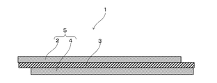
- FIG. 1 is a sectional view schematically showing a preferred embodiment of an electricity storage device according to the present invention.
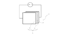
- FIG. 2 is a configuration diagram schematically showing an example of measurement of relative permittivity by an electricity storage device.
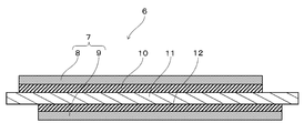
- FIG. 3 is a schematic diagram of an electricity storage device using a separator.
- the electricity storage device 1 has an upper electrode 2, a lower electrode 4, and a clay dielectric 3 between them.
- the clay dielectric 3 is the above-mentioned silicate compound or smectite clay mineral having a plate crystal structure. Smectite clay minerals include montmorillonite, hectorite, stevensite, and saponite.
- a metal current collector is used for the upper electrode 2 and the lower electrode 4 in which a thin film or powdery clay mineral is sandwiched.
- the upper electrode 2 and the lower electrode 4 may be in contact with the clay dielectric 3.
- the thickness of the dielectric is preferably 0.01 to 1 mm, but is not limited to this.
- This electricity storage device stores electricity due to the fine structure of clay.
- the above electricity storage device 1 is preferably sealed with a waterproof and gas barrier material in order to control the water content of the clay dielectric 3.
- a method of sealing using a metal case, or a method of using a lamination method to prevent evaporation of water by covering the film may be used.
- the film used at this time preferably has excellent water resistance, water vapor barrier properties, and gas barrier properties.
- the water content of the clay dielectric 3 is preferably 1 to 20% by mass, more preferably 5 to 15% by mass.
- the clay mineral at least one kind of clay selected from natural or synthetic clay is used. Such clay may be unmodified or modified, but at least one selected from smectite clays such as bentonite and hectorite is preferable. Among these, bentonite is an inorganic clay that is naturally produced and therefore has excellent safety. In addition, it is stable for a long period of time without being decomposed by microorganisms in the soil, and the price is low. Therefore, it is a particularly preferable clay mineral. As the clay mineral, one type of clay selected from bentonite and smectite can be used alone, or two types of clay can be used. The interlayer ions of bentonite and smectite are not particularly limited.
- the plate-shaped crystal structure smectite refers to, for example, a plate-shaped clay crystal having a thickness of about 1 nm and an aspect ratio of width/thickness of preferably 20 to 2000, more preferably about 30 to 300.
- Aspect ratios of typical smectite products are shown in Table 1, but the present invention is not limited thereto.
- the upper electrode 2 or the lower electrode coated with the same clay dispersion liquid again is applied as a dispersion liquid on the surfaces of the upper electrode 2 and the lower electrode 4 and naturally dried (usually water content 10% by mass) It is desirable to apply the dispersion liquid to the electrode 4 again, attach the dispersion liquid, and naturally dry it.
- a clay mineral When applying the clay mineral to the upper electrode 2 or the lower electrode 4, it is desirable to disperse the clay mineral in a solvent such as water before applying.
- a solvent such as water
- the dispersion medium one that can be dissolved and dispersed depending on the characteristics of clay can be used. It is also possible to form a layer of clay mineral between the upper electrode 2 and the lower electrode 4 in a powder state, but it is necessary to take measures so as to prevent scattering, control the coating thickness, and prevent defects.
- a clay mineral may be fixed between the electrodes by using a binder.
- the binder include styrene-butadiene rubber type, acrylic polymer type, polyvinylidene fluoride type and polytetrafluoroethylene type.
- various additive components can be optionally added to the clay dielectric as long as the object of the present invention is not impaired.
- the upper electrode 2 or the lower electrode 4 is made of, for example, a metal such as Pt, Au, Ti, Ag, Cu, Pb, Fe, Cd, Al, Zn, Mg or Li, and stainless steel, brass (Cu-Zn), cast iron, It is preferable to use steel, an alloy such as an aluminum alloy, or a current collector such as graphite or a conductive polymer.
- the electrodes 2, 4, and 7 may be functionalized by surface-treating any of them.
- Surface treatment methods include metal thin film coating, electroless plating, vapor phase plating (CVD method), anodic etching method, anodic oxidation chemical conversion, electrolytic polishing, chemical modification, electroforming, carbon coating, and carbide treatment. and so on.
- the anodic oxide coating of aluminum is a preferable electrode because it has excellent corrosion resistance and abrasion resistance.
- a separator may be used between the upper and lower electrodes to prevent a short circuit.
- An electricity storage device 6 using the separator 11 is shown in FIG.
- the separator 11 isolates the dielectrics 10 and 12 between the upper electrode 8 and the lower electrode 9, prevents contact between upper and lower electrodes and short circuit of current, and allows metal ions and electrons to pass through.
- the type of the separator 11 is not particularly limited, and may be made of, for example, an olefin resin, a PDF resin, a PAN resin, a PMMA resin, or the like.
- the separator 11 is impregnated with a dispersion liquid of clay serving as a dielectric and is naturally dried.
- the clay aqueous dispersion is a clay mineral, Kunipia F (trade name, manufactured by Kunimine Industry Co., Ltd.) (Example 1), Smecton ST (trade name, manufactured by Kunimine Industry Co., Ltd.) (Example 2), Smecton SA (trade name, Kunimine Co., Ltd.) Kogyo Co., Ltd. (Example 3) and Smecton SWN (trade name, manufactured by Kunimine Industry Co., Ltd.) (Example 4) were used.
- Kunipia F is a clay mineral obtained by refining bentonite, which is a natural product whose main component is montmorillonite (Na ions are intercalated between layers).
- Smecton ST is a synthetic clay containing stevensite as a main component (Na ion is intercalated between layers).
- Smecton SA is a synthetic clay whose main component is saponite (Na ions are intercalated between layers).
- Smecton SWN is a synthetic clay whose main component is hectorite (Na ions are intercalated between layers).
- Table 2 shows the cation exchange capacity CEC [meq/100 g] of the clay used in each example.
- Table 3 shows the results of measuring the relative dielectric constants of Examples 1 to 4 at 100 Hz and 10 kHz.
- Examples 1 to 4 obtained high relative permittivity in the electricity storage device using the smecton clay mineral as the dielectric. This shows that an inexpensive electricity storage device with a high dielectric constant can be manufactured. An electricity storage device using smecton SWN can obtain the highest relative permittivity and is most preferable as an electricity storage device.
- Examples 5-8 ⁇ Measurement of relative permittivity of electricity storage device with different collector>
- the current collector metal was changed to aluminum or brass and Kunipia F or smecton ST was used as the dielectric in the production of the above electricity storage device.
- Smecton ST was used for the clay dielectric 3
- brass was used for the electrode in the method for producing the electricity storage device.
- Example 9 SUS was used as the electrode 5 and Kunipia RC-G (manufactured by Kunimine Industries Co., Ltd.) was used as the dielectric in the method for manufacturing the electricity storage device.
- Kunipia RC-G is a smectite clay in which interlayer ions of Kunipia F are replaced with lithium ions (CEC40 [meq/100 g]).
- SUS was used as a current collector and Kunibis 110 (manufactured by Kunimine Industries Co., Ltd.) was used as a dielectric in the method for producing the electricity storage device.
- Kunibis 110 is an organically modified smectite clay in which interlayer ions of Kunipia F are replaced with sodium ions by trimethylstearyl ammonium ions.
- Table 6 shows the results of measuring the relative permittivity of Examples 9 and 10 at 100 Hz and 10 kHz.
- Examples 11 and 12 As shown in FIG. 3, a clay dispersion was applied onto the upper electrode 8 and the lower electrode 9 to form an upper dielectric 10 and a lower dielectric 12. The clay-impregnated separator 11 impregnated with the clay dispersion was sandwiched between the upper dielectric 10 and the lower dielectric 12 to form the electricity storage device 6.
- Kunipia F was used as the dielectric
- SUS430 was used as the electrode in the method of manufacturing the electricity storage device 6 described above.
- Example 12 uses Smecton ST as a dielectric and SUS430 as an electrode in the method of manufacturing the electricity storage device 6 described above.
- Example 11 and Example 12 were measured.
- Table 7 shows the measurement results of the relative permittivity of Examples 11 and 12.
- Example 13 and Example 14 were measured.
- Table 8 shows the measurement results of the relative dielectric constants of Example 13 and Example 14.
Landscapes
- Engineering & Computer Science (AREA)
- Power Engineering (AREA)
- Chemical & Material Sciences (AREA)
- Microelectronics & Electronic Packaging (AREA)
- Manufacturing & Machinery (AREA)
- Ceramic Engineering (AREA)
- Inorganic Chemistry (AREA)
- Organic Chemistry (AREA)
- Materials Engineering (AREA)
- Electrochemistry (AREA)
- Chemical Kinetics & Catalysis (AREA)
- Dispersion Chemistry (AREA)
- General Chemical & Material Sciences (AREA)
- Electric Double-Layer Capacitors Or The Like (AREA)
- Silicates, Zeolites, And Molecular Sieves (AREA)
- Fixed Capacitors And Capacitor Manufacturing Machines (AREA)
Abstract
La présente invention concerne un dispositif de stockage d'énergie ayant deux électrodes et un film d'argile à base de smectite ayant une structure de cristal en plaquettes entre les électrodes.
Priority Applications (2)
| Application Number | Priority Date | Filing Date | Title |
|---|---|---|---|
| CN202080009833.8A CN113302154B (zh) | 2019-02-08 | 2020-01-08 | 蓄电器件 |
| US17/424,428 US11718533B2 (en) | 2019-02-08 | 2020-01-08 | Power storage device |
Applications Claiming Priority (2)
| Application Number | Priority Date | Filing Date | Title |
|---|---|---|---|
| JP2019-022129 | 2019-02-08 | ||
| JP2019022129A JP7235292B2 (ja) | 2019-02-08 | 2019-02-08 | 蓄電デバイス |
Publications (1)
| Publication Number | Publication Date |
|---|---|
| WO2020162092A1 true WO2020162092A1 (fr) | 2020-08-13 |
Family
ID=71947816
Family Applications (1)
| Application Number | Title | Priority Date | Filing Date |
|---|---|---|---|
| PCT/JP2020/000333 Ceased WO2020162092A1 (fr) | 2019-02-08 | 2020-01-08 | Dispositif de stockage d'énergie |
Country Status (4)
| Country | Link |
|---|---|
| US (1) | US11718533B2 (fr) |
| JP (1) | JP7235292B2 (fr) |
| CN (1) | CN113302154B (fr) |
| WO (1) | WO2020162092A1 (fr) |
Families Citing this family (1)
| Publication number | Priority date | Publication date | Assignee | Title |
|---|---|---|---|---|
| JP7276297B2 (ja) * | 2020-10-08 | 2023-05-18 | 株式会社豊田中央研究所 | 複合誘電体材料 |
Citations (6)
| Publication number | Priority date | Publication date | Assignee | Title |
|---|---|---|---|---|
| JPH10269844A (ja) * | 1997-03-27 | 1998-10-09 | Tdk Corp | 固体状電解質とリチウム二次電池と電気二重層キャパシタ |
| JP2008130844A (ja) * | 2006-11-21 | 2008-06-05 | Matsushita Electric Ind Co Ltd | 全固体型電気二重層コンデンサー |
| US20140254062A1 (en) * | 2013-03-05 | 2014-09-11 | Davood Namdar Khojasteh | Multi layer Smectite Capacitor (MLSC) |
| WO2017138382A1 (fr) * | 2016-02-12 | 2017-08-17 | Necエナジーデバイス株式会社 | Électrode positive pour batterie secondaire au lithium-ion ainsi que procédé de fabrication de celle-ci, batterie secondaire au lithium-ion, et procédé d'évaluation |
| JP2018041670A (ja) * | 2016-09-08 | 2018-03-15 | クニミネ工業株式会社 | アルミニウム電池 |
| WO2018096910A1 (fr) * | 2016-11-24 | 2018-05-31 | Jxtgエネルギー株式会社 | Composition élastomère thermoplastique conductrice |
Family Cites Families (2)
| Publication number | Priority date | Publication date | Assignee | Title |
|---|---|---|---|---|
| JPH08153646A (ja) * | 1994-11-30 | 1996-06-11 | Mitsubishi Materials Corp | 積層セラミックコンデンサ及びその製造方法 |
| JP2007098707A (ja) * | 2005-10-03 | 2007-04-19 | Asahi Kasei Electronics Co Ltd | 誘電体層形成用塗工液及びシート |
-
2019
- 2019-02-08 JP JP2019022129A patent/JP7235292B2/ja active Active
-
2020
- 2020-01-08 WO PCT/JP2020/000333 patent/WO2020162092A1/fr not_active Ceased
- 2020-01-08 CN CN202080009833.8A patent/CN113302154B/zh active Active
- 2020-01-08 US US17/424,428 patent/US11718533B2/en active Active
Patent Citations (6)
| Publication number | Priority date | Publication date | Assignee | Title |
|---|---|---|---|---|
| JPH10269844A (ja) * | 1997-03-27 | 1998-10-09 | Tdk Corp | 固体状電解質とリチウム二次電池と電気二重層キャパシタ |
| JP2008130844A (ja) * | 2006-11-21 | 2008-06-05 | Matsushita Electric Ind Co Ltd | 全固体型電気二重層コンデンサー |
| US20140254062A1 (en) * | 2013-03-05 | 2014-09-11 | Davood Namdar Khojasteh | Multi layer Smectite Capacitor (MLSC) |
| WO2017138382A1 (fr) * | 2016-02-12 | 2017-08-17 | Necエナジーデバイス株式会社 | Électrode positive pour batterie secondaire au lithium-ion ainsi que procédé de fabrication de celle-ci, batterie secondaire au lithium-ion, et procédé d'évaluation |
| JP2018041670A (ja) * | 2016-09-08 | 2018-03-15 | クニミネ工業株式会社 | アルミニウム電池 |
| WO2018096910A1 (fr) * | 2016-11-24 | 2018-05-31 | Jxtgエネルギー株式会社 | Composition élastomère thermoplastique conductrice |
Also Published As
| Publication number | Publication date |
|---|---|
| CN113302154B (zh) | 2024-07-12 |
| US11718533B2 (en) | 2023-08-08 |
| US20220089450A1 (en) | 2022-03-24 |
| JP7235292B2 (ja) | 2023-03-08 |
| CN113302154A (zh) | 2021-08-24 |
| JP2020129625A (ja) | 2020-08-27 |
Similar Documents
| Publication | Publication Date | Title |
|---|---|---|
| Ghidiu et al. | Conductive two-dimensional titanium carbide ‘clay’with high volumetric capacitance | |
| Pinto et al. | Synthesis and electrochemical properties of 2D molybdenum vanadium carbides–solid solution MXenes | |
| Torkamanzadeh et al. | MXene/activated-carbon hybrid capacitive deionization for permselective ion removal at low and high salinity | |
| Maharsi et al. | Electrochemical properties of TiO x/rGO composite as an electrode for supercapacitors | |
| Naguib et al. | Ti 3 C 2 T x (MXene)–polyacrylamide nanocomposite films | |
| Buczek et al. | Rational design of titanium carbide MXene electrode architectures for hybrid capacitive deionization | |
| Zhang et al. | Electrolyte-mediated dense integration of graphene-MXene films for high volumetric capacitance flexible supercapacitors | |
| Chaudhari et al. | MXene: an emerging two-dimensional material for future energy conversion and storage applications | |
| Boota et al. | Pseudocapacitive electrodes produced by oxidant-free polymerization of pyrrole between the layers of 2D titanium carbide (MXene) | |
| Argüello et al. | Electrophoretic deposition of manganese oxide and graphene nanoplatelets on graphite paper for the manufacture of supercapacitor electrodes | |
| Sahoo et al. | Nano gold decorated reduced graphene oxide wrapped polymethylmethacrylate for supercapacitor applications | |
| CN114026663A (zh) | 导电性材料、导电性薄膜、电化学电容器、导电性材料的制造方法及导电性薄膜的制造方法 | |
| JP2013512554A (ja) | 電子電池に応用されるコア−シェルナノ粒子 | |
| Qian et al. | Capacitance changes associated with cation-transport in free-standing flexible Ti3C2Tx (TO, F, OH) MXene film electrodes | |
| KR20180108725A (ko) | 고도로 배향되고 밀집된 그래핀 시트를 갖는 슈퍼커패시터 전극 및 생산 공정 | |
| Chen et al. | Graphene based integrated tandem supercapacitors fabricated directly on separators | |
| TW201639220A (zh) | 電極材料及能量儲存設備 | |
| JP7487783B2 (ja) | 導電性2次元粒子およびその製造方法 | |
| WO2006070617A1 (fr) | Element d'electrode polarisable, procede pour sa fabrication et condensateur electrochimique utilisant ledit element | |
| Borgohain et al. | Ternary composites of delaminated-MnO 2/PDDA/functionalized-CNOs for high-capacity supercapacitor electrodes | |
| Jeong et al. | One-pot synthesis of thin Co (OH) 2 nanosheets on graphene and their high activity as a capacitor electrode | |
| Tsyganov et al. | Molten salt-shielded synthesis of Ti 3 AlC 2 as a precursor for large-scale preparation of Ti 3 C 2 T x MXene binder-free film electrode supercapacitors | |
| WO2023047861A1 (fr) | Composition contenant des particules bidimensionnelles conductrices, film conducteur, et procédé de fabrication d'une composition contenant des particules bidimensionnelles conductrices | |
| Delfani et al. | A 3D binder-free rGO/NiMnCo nanosheet for highly efficient hybrid supercapacitors and ion-selective capacitive deionization | |
| WO2020162092A1 (fr) | Dispositif de stockage d'énergie |
Legal Events
| Date | Code | Title | Description |
|---|---|---|---|
| 121 | Ep: the epo has been informed by wipo that ep was designated in this application |
Ref document number: 20752860 Country of ref document: EP Kind code of ref document: A1 |
|
| NENP | Non-entry into the national phase |
Ref country code: DE |
|
| 122 | Ep: pct application non-entry in european phase |
Ref document number: 20752860 Country of ref document: EP Kind code of ref document: A1 |