WO2020174732A1 - Capteur infrarouge et réseau de capteurs infrarouges - Google Patents
Capteur infrarouge et réseau de capteurs infrarouges Download PDFInfo
- Publication number
- WO2020174732A1 WO2020174732A1 PCT/JP2019/037205 JP2019037205W WO2020174732A1 WO 2020174732 A1 WO2020174732 A1 WO 2020174732A1 JP 2019037205 W JP2019037205 W JP 2019037205W WO 2020174732 A1 WO2020174732 A1 WO 2020174732A1
- Authority
- WO
- WIPO (PCT)
- Prior art keywords
- infrared sensor
- infrared
- base substrate
- light receiving
- wiring
- Prior art date
- Legal status (The legal status is an assumption and is not a legal conclusion. Google has not performed a legal analysis and makes no representation as to the accuracy of the status listed.)
- Ceased
Links
Images















Classifications
-
- G—PHYSICS
- G01—MEASURING; TESTING
- G01J—MEASUREMENT OF INTENSITY, VELOCITY, SPECTRAL CONTENT, POLARISATION, PHASE OR PULSE CHARACTERISTICS OF INFRARED, VISIBLE OR ULTRAVIOLET LIGHT; COLORIMETRY; RADIATION PYROMETRY
- G01J5/00—Radiation pyrometry, e.g. infrared or optical thermometry
- G01J5/10—Radiation pyrometry, e.g. infrared or optical thermometry using electric radiation detectors
- G01J5/20—Radiation pyrometry, e.g. infrared or optical thermometry using electric radiation detectors using resistors, thermistors or semiconductors sensitive to radiation, e.g. photoconductive devices
-
- G—PHYSICS
- G01—MEASURING; TESTING
- G01J—MEASUREMENT OF INTENSITY, VELOCITY, SPECTRAL CONTENT, POLARISATION, PHASE OR PULSE CHARACTERISTICS OF INFRARED, VISIBLE OR ULTRAVIOLET LIGHT; COLORIMETRY; RADIATION PYROMETRY
- G01J5/00—Radiation pyrometry, e.g. infrared or optical thermometry
- G01J5/02—Constructional details
- G01J5/0225—Shape of the cavity itself or of elements contained in or suspended over the cavity
- G01J5/024—Special manufacturing steps or sacrificial layers or layer structures
-
- G—PHYSICS
- G01—MEASURING; TESTING
- G01J—MEASUREMENT OF INTENSITY, VELOCITY, SPECTRAL CONTENT, POLARISATION, PHASE OR PULSE CHARACTERISTICS OF INFRARED, VISIBLE OR ULTRAVIOLET LIGHT; COLORIMETRY; RADIATION PYROMETRY
- G01J5/00—Radiation pyrometry, e.g. infrared or optical thermometry
- G01J5/02—Constructional details
- G01J5/08—Optical arrangements
- G01J5/0813—Planar mirrors; Parallel phase plates
-
- G—PHYSICS
- G01—MEASURING; TESTING
- G01J—MEASUREMENT OF INTENSITY, VELOCITY, SPECTRAL CONTENT, POLARISATION, PHASE OR PULSE CHARACTERISTICS OF INFRARED, VISIBLE OR ULTRAVIOLET LIGHT; COLORIMETRY; RADIATION PYROMETRY
- G01J5/00—Radiation pyrometry, e.g. infrared or optical thermometry
- G01J5/10—Radiation pyrometry, e.g. infrared or optical thermometry using electric radiation detectors
- G01J5/20—Radiation pyrometry, e.g. infrared or optical thermometry using electric radiation detectors using resistors, thermistors or semiconductors sensitive to radiation, e.g. photoconductive devices
- G01J5/22—Electrical features thereof
-
- H—ELECTRICITY
- H10—SEMICONDUCTOR DEVICES; ELECTRIC SOLID-STATE DEVICES NOT OTHERWISE PROVIDED FOR
- H10F—INORGANIC SEMICONDUCTOR DEVICES SENSITIVE TO INFRARED RADIATION, LIGHT, ELECTROMAGNETIC RADIATION OF SHORTER WAVELENGTH OR CORPUSCULAR RADIATION
- H10F39/00—Integrated devices, or assemblies of multiple devices, comprising at least one element covered by group H10F30/00, e.g. radiation detectors comprising photodiode arrays
- H10F39/10—Integrated devices
-
- H—ELECTRICITY
- H10—SEMICONDUCTOR DEVICES; ELECTRIC SOLID-STATE DEVICES NOT OTHERWISE PROVIDED FOR
- H10N—ELECTRIC SOLID-STATE DEVICES NOT OTHERWISE PROVIDED FOR
- H10N15/00—Thermoelectric devices without a junction of dissimilar materials; Thermomagnetic devices, e.g. using the Nernst-Ettingshausen effect
-
- H—ELECTRICITY
- H10—SEMICONDUCTOR DEVICES; ELECTRIC SOLID-STATE DEVICES NOT OTHERWISE PROVIDED FOR
- H10N—ELECTRIC SOLID-STATE DEVICES NOT OTHERWISE PROVIDED FOR
- H10N19/00—Integrated devices, or assemblies of multiple devices, comprising at least one thermoelectric or thermomagnetic element covered by groups H10N10/00 - H10N15/00
-
- G—PHYSICS
- G01—MEASURING; TESTING
- G01J—MEASUREMENT OF INTENSITY, VELOCITY, SPECTRAL CONTENT, POLARISATION, PHASE OR PULSE CHARACTERISTICS OF INFRARED, VISIBLE OR ULTRAVIOLET LIGHT; COLORIMETRY; RADIATION PYROMETRY
- G01J5/00—Radiation pyrometry, e.g. infrared or optical thermometry
- G01J5/10—Radiation pyrometry, e.g. infrared or optical thermometry using electric radiation detectors
- G01J5/20—Radiation pyrometry, e.g. infrared or optical thermometry using electric radiation detectors using resistors, thermistors or semiconductors sensitive to radiation, e.g. photoconductive devices
- G01J2005/206—Radiation pyrometry, e.g. infrared or optical thermometry using electric radiation detectors using resistors, thermistors or semiconductors sensitive to radiation, e.g. photoconductive devices on foils
Definitions
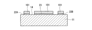
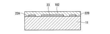
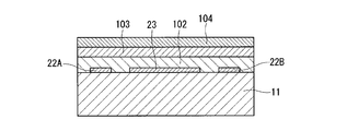
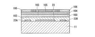
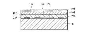
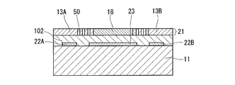
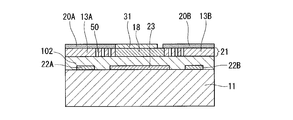
- FIG. 20M is a schematic cross-sectional view for explaining the example of the method for manufacturing the infrared sensor of the present disclosure.
- FIG. 20N is a schematic cross-sectional view for explaining the example of the method for manufacturing the infrared sensor of the present disclosure.
- FIG. 20O is a schematic cross-sectional view for explaining an example of the method for manufacturing the infrared sensor of the present disclosure.
- the above structure is expected to improve the sensitivity of receiving infrared rays.
- an infrared reflective film is usually provided on the surface of the base substrate at a position facing the infrared light receiving portion in order to increase the amount of infrared light absorbed in the infrared light receiving portion.
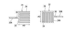
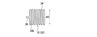
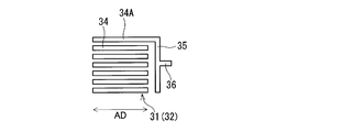
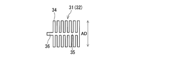
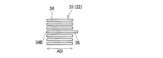
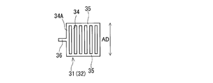
- the electrode having the L/S structure can have polarization selection ability with respect to infrared rays. Further, due to the existence of the strip-shaped portion 34A to which the connection line 36 is electrically connected, the electrode can function as an electrode for measuring the electric resistance of the resistance change film 33. In the lower electrode 31 and/or the upper electrode 32 of FIG. 3B, the strip portions 34 are not physically or electrically connected to each other. However, the bus line 35 is connected to one end of the strip portion 34A located at the end of the array. A connection line 36 is connected from the bus line 35 to the side opposite to the side where the strip portions 34 are arranged and parallel to the alignment direction AD.
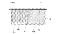
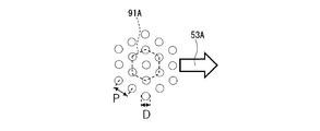
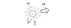
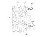
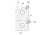
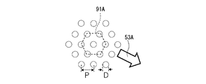
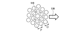
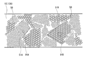
- the type of unit cell 91A in the first domain 51A and the type of unit cell 91B in the second domain 51B are the same.
- the unit lattice 91A and the unit lattice 91B of FIG. 4A are both hexagonal lattices.
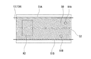
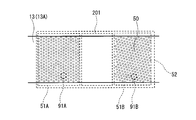
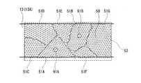
- the phononic crystal structure A of FIGS. 9 and 10 has a second domain 51B that is not in contact with the side of the beam 13 (13A).
- the cycle P of the arrangement of the through holes 50 is, for example, 1 nm or more and 300 nm or less. This is because the wavelengths of phonons that carry heat range primarily from 1 nm to 300 nm.
- the period P is determined by the center-to-center distance between adjacent through holes 50 in plan view (see FIGS. 14A and 14B).
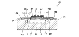
- the infrared sensor of the third embodiment is shown in FIG.
- the infrared sensor 1C shown in FIG. 19 is a bolometer-type infrared sensor which is a type of thermal infrared sensor.
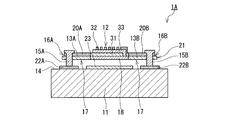
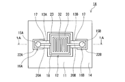
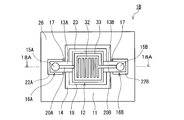
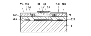
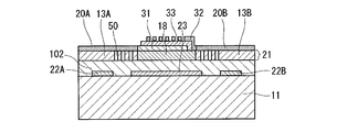
- the infrared sensor 1C includes a base substrate 11, a bolometer infrared light receiver 12, a first beam 13A, a second beam 13B, a first wiring 20A, a second wiring 20B, and an infrared reflecting film 23.
- the first beam 13A and the second beam 13B respectively have connecting portions 16A and 16B connected to the base substrate 11.
- Each of the first beam 13 ⁇ /b>A and the second beam 13 ⁇ /b>B has a separating portion 17 that is separated from the base substrate 11.
Landscapes
- Physics & Mathematics (AREA)
- General Physics & Mathematics (AREA)
- Spectroscopy & Molecular Physics (AREA)
- Engineering & Computer Science (AREA)
- Manufacturing & Machinery (AREA)
- Photometry And Measurement Of Optical Pulse Characteristics (AREA)
- Solid State Image Pick-Up Elements (AREA)
Abstract
La présente invention concerne une technologie qui permet d'augmenter la sensibilité d'un capteur infrarouge. Le capteur infrarouge de la présente invention comprend : un substrat de base ; une partie réception de lumière infrarouge ; un premier faisceau ; un second faisceau ; un premier câblage ; un second câblage ; et un film réfléchissant les infrarouges. Le premier faisceau et le second faisceau comprennent une partie liaison reliée au substrat de base et/ou à un élément sur le substrat de base, et une partie séparée qui est séparée du substrat de base, les premier et second faisceaux étant physiquement reliés à la partie réception de lumière infrarouge par les parties séparées. La partie réception de lumière infrarouge est maintenue par les premier et second faisceaux de façon à être séparée du substrat de base, et comprend une électrode inférieure, une électrode supérieure et un film à changement de résistance. Le film à changement de résistance est pris en sandwich dans la direction de l'épaisseur par l'électrode inférieure et l'électrode supérieure, l'électrode inférieure et l'électrode supérieure sont chacune connectées électriquement au film à changement de résistance, l'électrode inférieure et l'électrode supérieure sont connectées électriquement au premier câblage et au second câblage, respectivement, au moins une électrode parmi l'électrode inférieure et l'électrode supérieure présente une structure de ligne et d'espace, et le film réfléchissant les infrarouges est situé dans un emplacement, à l'intérieur de la surface de substrat de base, faisant face à la partie réception de lumière infrarouge.
Priority Applications (4)
| Application Number | Priority Date | Filing Date | Title |
|---|---|---|---|
| CN201980075092.0A CN113015890B (zh) | 2019-02-28 | 2019-09-24 | 红外线传感器及红外线传感器阵列 |
| JP2021501541A JP7603247B2 (ja) | 2019-02-28 | 2019-09-24 | 赤外線センサ及び赤外線センサアレイ |
| EP19917332.9A EP3933357B1 (fr) | 2019-02-28 | 2019-09-24 | Capteur infrarouge et réseau de capteurs infrarouges |
| US17/347,467 US12007283B2 (en) | 2019-02-28 | 2021-06-14 | Infrared sensor and infrared sensor array |
Applications Claiming Priority (2)
| Application Number | Priority Date | Filing Date | Title |
|---|---|---|---|
| JP2019035360 | 2019-02-28 | ||
| JP2019-035360 | 2019-02-28 |
Related Child Applications (1)
| Application Number | Title | Priority Date | Filing Date |
|---|---|---|---|
| US17/347,467 Continuation US12007283B2 (en) | 2019-02-28 | 2021-06-14 | Infrared sensor and infrared sensor array |
Publications (1)
| Publication Number | Publication Date |
|---|---|
| WO2020174732A1 true WO2020174732A1 (fr) | 2020-09-03 |
Family
ID=72240206
Family Applications (1)
| Application Number | Title | Priority Date | Filing Date |
|---|---|---|---|
| PCT/JP2019/037205 Ceased WO2020174732A1 (fr) | 2019-02-28 | 2019-09-24 | Capteur infrarouge et réseau de capteurs infrarouges |
Country Status (5)
| Country | Link |
|---|---|
| US (1) | US12007283B2 (fr) |
| EP (1) | EP3933357B1 (fr) |
| JP (1) | JP7603247B2 (fr) |
| CN (1) | CN113015890B (fr) |
| WO (1) | WO2020174732A1 (fr) |
Cited By (2)
| Publication number | Priority date | Publication date | Assignee | Title |
|---|---|---|---|---|
| WO2022138247A1 (fr) * | 2020-12-25 | 2022-06-30 | パナソニックIpマネジメント株式会社 | Matériau solide |
| WO2022138248A1 (fr) * | 2020-12-25 | 2022-06-30 | パナソニックIpマネジメント株式会社 | Capteur à infrarouge |
Families Citing this family (4)
| Publication number | Priority date | Publication date | Assignee | Title |
|---|---|---|---|---|
| JP7232978B2 (ja) * | 2017-12-11 | 2023-03-06 | パナソニックIpマネジメント株式会社 | 赤外線センサおよび赤外線センサのボロメータ赤外線受光部を冷却する方法 |
| KR102830278B1 (ko) * | 2020-05-27 | 2025-07-04 | 삼성전자주식회사 | 적외선 센서가 통합된 이미지 센서 및 이를 포함하는 전자 장치 |
| US12345575B2 (en) * | 2021-05-11 | 2025-07-01 | America as represented by the Secretary of the Army | Phonon disruptors for increased thermal resistance without sacrificing electrical signal quality in thermal sensors |
| KR102926962B1 (ko) * | 2021-06-29 | 2026-02-11 | 삼성전자주식회사 | 열 또는 적외선 감지용 센서 및 이를 포함하는 전자장치 |
Citations (7)
| Publication number | Priority date | Publication date | Assignee | Title |
|---|---|---|---|---|
| JPH08201177A (ja) * | 1995-01-20 | 1996-08-09 | Nec Corp | 赤外線検出器及びその駆動方法 |
| JPH0915039A (ja) * | 1995-06-27 | 1997-01-17 | Matsushita Electric Works Ltd | 赤外線検出素子及び赤外線検出素子アレイ |
| US5912464A (en) * | 1996-08-08 | 1999-06-15 | Commissariat Al'energie Atomique | Infrared detector and manufacturing process |
| JP2001272271A (ja) * | 2000-01-17 | 2001-10-05 | Mitsubishi Electric Corp | 赤外線センサ |
| JP2008003081A (ja) * | 2006-05-25 | 2008-01-10 | Matsushita Electric Works Ltd | 赤外線センサー |
| JP2008082790A (ja) * | 2006-09-26 | 2008-04-10 | Matsushita Electric Works Ltd | 赤外線センサ |
| JP2017223644A (ja) | 2016-06-13 | 2017-12-21 | パナソニックIpマネジメント株式会社 | 赤外線センサ |
Family Cites Families (17)
| Publication number | Priority date | Publication date | Assignee | Title |
|---|---|---|---|---|
| JP3129504B2 (ja) * | 1992-02-25 | 2001-01-31 | 松下電工株式会社 | 赤外線検出素子 |
| JP3249174B2 (ja) | 1992-05-22 | 2002-01-21 | テルモ株式会社 | 赤外線センサおよびその製造方法 |
| JP3246131B2 (ja) * | 1993-10-29 | 2002-01-15 | 松下電工株式会社 | 赤外線検出素子の製造方法 |
| JP3460810B2 (ja) * | 1999-07-26 | 2003-10-27 | 日本電気株式会社 | 熱分離構造を有する熱型赤外線検出器 |
| JP2003106896A (ja) * | 2001-10-01 | 2003-04-09 | Mitsubishi Electric Corp | 赤外線センサ及びその製造方法 |
| FR2864065B1 (fr) * | 2003-12-22 | 2006-02-24 | Univ Toulouse | Utilisation de ferrites spinelles comme materiau sensible pour dispositifs bolometriques de detection de l'infrarouge. |
| JP2005043381A (ja) * | 2004-10-18 | 2005-02-17 | Nec Corp | 熱型赤外線検出器およびその製造方法 |
| EP2021749B1 (fr) * | 2006-05-25 | 2013-01-23 | Panasonic Corporation | Capteur d'infrarouge |
| JP2010237118A (ja) * | 2009-03-31 | 2010-10-21 | Panasonic Electric Works Co Ltd | 赤外線アレイセンサ |
| CN102356305A (zh) * | 2010-05-27 | 2012-02-15 | 松下电器产业株式会社 | 热电变换器件和辐射检测器以及使用它的辐射检测方法 |
| JP5838343B2 (ja) * | 2010-06-25 | 2016-01-06 | パナソニックIpマネジメント株式会社 | 焦電型赤外線検知素子およびそれを用いた赤外線センサ |
| US20140042324A1 (en) * | 2012-08-08 | 2014-02-13 | Agency For Science, Technology And Research | Detector and method of controlling the same |
| US10677656B2 (en) * | 2012-12-31 | 2020-06-09 | Flir Systems, Inc. | Devices and methods for infrared reference pixels |
| US9417465B2 (en) | 2013-04-07 | 2016-08-16 | The Regents Of The University Of Colorado, A Body Corporate | Nanophononic metamaterials |
| JP2016039392A (ja) | 2014-08-05 | 2016-03-22 | ソニー株式会社 | 撮像装置及び画素信号読み出し方法 |
| JP6486695B2 (ja) * | 2015-01-14 | 2019-03-20 | 浜松ホトニクス株式会社 | ボロメータ型THz検出器 |
| EP3410083A4 (fr) * | 2016-01-29 | 2019-09-04 | Mitsubishi Materials Corporation | Capteur infrarouge |
-
2019
- 2019-09-24 WO PCT/JP2019/037205 patent/WO2020174732A1/fr not_active Ceased
- 2019-09-24 JP JP2021501541A patent/JP7603247B2/ja active Active
- 2019-09-24 EP EP19917332.9A patent/EP3933357B1/fr active Active
- 2019-09-24 CN CN201980075092.0A patent/CN113015890B/zh active Active
-
2021
- 2021-06-14 US US17/347,467 patent/US12007283B2/en active Active
Patent Citations (7)
| Publication number | Priority date | Publication date | Assignee | Title |
|---|---|---|---|---|
| JPH08201177A (ja) * | 1995-01-20 | 1996-08-09 | Nec Corp | 赤外線検出器及びその駆動方法 |
| JPH0915039A (ja) * | 1995-06-27 | 1997-01-17 | Matsushita Electric Works Ltd | 赤外線検出素子及び赤外線検出素子アレイ |
| US5912464A (en) * | 1996-08-08 | 1999-06-15 | Commissariat Al'energie Atomique | Infrared detector and manufacturing process |
| JP2001272271A (ja) * | 2000-01-17 | 2001-10-05 | Mitsubishi Electric Corp | 赤外線センサ |
| JP2008003081A (ja) * | 2006-05-25 | 2008-01-10 | Matsushita Electric Works Ltd | 赤外線センサー |
| JP2008082790A (ja) * | 2006-09-26 | 2008-04-10 | Matsushita Electric Works Ltd | 赤外線センサ |
| JP2017223644A (ja) | 2016-06-13 | 2017-12-21 | パナソニックIpマネジメント株式会社 | 赤外線センサ |
Non-Patent Citations (1)
| Title |
|---|
| A. KOSAREV ET AL.: "Un-cooled Micro-bolometer with Sandwiched Thermo-sensing Layer Based on Ge Films Deposited by Plasma", MATER. RES. SOC. SYMP. PROC., vol. 910, 2006 |
Cited By (4)
| Publication number | Priority date | Publication date | Assignee | Title |
|---|---|---|---|---|
| WO2022138247A1 (fr) * | 2020-12-25 | 2022-06-30 | パナソニックIpマネジメント株式会社 | Matériau solide |
| WO2022138248A1 (fr) * | 2020-12-25 | 2022-06-30 | パナソニックIpマネジメント株式会社 | Capteur à infrarouge |
| JP2022102826A (ja) * | 2020-12-25 | 2022-07-07 | パナソニックIpマネジメント株式会社 | 固体材料 |
| JP2022102827A (ja) * | 2020-12-25 | 2022-07-07 | パナソニックIpマネジメント株式会社 | 赤外線センサ |
Also Published As
| Publication number | Publication date |
|---|---|
| CN113015890A (zh) | 2021-06-22 |
| US20210302236A1 (en) | 2021-09-30 |
| EP3933357A4 (fr) | 2022-07-20 |
| JPWO2020174732A1 (ja) | 2021-12-23 |
| CN113015890B (zh) | 2024-04-02 |
| JP7603247B2 (ja) | 2024-12-20 |
| EP3933357A1 (fr) | 2022-01-05 |
| EP3933357B1 (fr) | 2023-11-01 |
| US12007283B2 (en) | 2024-06-11 |
Similar Documents
| Publication | Publication Date | Title |
|---|---|---|
| JP7352884B2 (ja) | 赤外線センサ及びフォノニック結晶体 | |
| JP7603247B2 (ja) | 赤外線センサ及び赤外線センサアレイ | |
| JP6311133B2 (ja) | 赤外線センサ | |
| JP7634204B2 (ja) | 赤外線センサ、赤外線センサアレイ、及び赤外線センサの製造方法 | |
| JP7232978B2 (ja) | 赤外線センサおよび赤外線センサのボロメータ赤外線受光部を冷却する方法 | |
| KR102605880B1 (ko) | 고 흡수 효율 및 신호대잡음 비를 갖는 현가 복사 멤브레인을 갖는 검출 디바이스 | |
| CN102538982A (zh) | 基于悬吊测辐射热微板的红外检测器 | |
| US20080265164A1 (en) | Thermal detector for electromagnetic radiation and infrared detection device using such detectors | |
| US8080797B2 (en) | Bolometer and method of producing a bolometer | |
| US20110198720A1 (en) | Thermal-type infrared solid-state imaging element | |
| US7232998B2 (en) | Bolometer-type infrared solid-state image sensor | |
| KR20080052169A (ko) | 볼로미터 및 그 제조 방법 | |
| KR100539395B1 (ko) | 2층 구조의 비냉각형 적외선 센서 | |
| WO2022239610A1 (fr) | Capteur de type thermopile et réseau de capteurs | |
| CN117730241A (zh) | 导电性绝热材料以及红外线传感器 | |
| WO2021241088A1 (fr) | Capteur infrarouge et procédé de commande de capteur infrarouge | |
| JP2004271386A (ja) | 熱型赤外線検出器及びその製造方法 |
Legal Events
| Date | Code | Title | Description |
|---|---|---|---|
| 121 | Ep: the epo has been informed by wipo that ep was designated in this application |
Ref document number: 19917332 Country of ref document: EP Kind code of ref document: A1 |
|
| ENP | Entry into the national phase |
Ref document number: 2021501541 Country of ref document: JP Kind code of ref document: A |
|
| NENP | Non-entry into the national phase |
Ref country code: DE |
|
| ENP | Entry into the national phase |
Ref document number: 2019917332 Country of ref document: EP Effective date: 20210928 |