WO2020195830A1 - Vibreur piézoélectrique et procédé de fabrication correspondant - Google Patents
Vibreur piézoélectrique et procédé de fabrication correspondant Download PDFInfo
- Publication number
- WO2020195830A1 WO2020195830A1 PCT/JP2020/010538 JP2020010538W WO2020195830A1 WO 2020195830 A1 WO2020195830 A1 WO 2020195830A1 JP 2020010538 W JP2020010538 W JP 2020010538W WO 2020195830 A1 WO2020195830 A1 WO 2020195830A1
- Authority
- WO
- WIPO (PCT)
- Prior art keywords
- piezoelectric
- excitation electrode
- surface layer
- chromium
- electrode
- Prior art date
- Legal status (The legal status is an assumption and is not a legal conclusion. Google has not performed a legal analysis and makes no representation as to the accuracy of the status listed.)
- Ceased
Links
Images








Classifications
-
- H—ELECTRICITY
- H03—ELECTRONIC CIRCUITRY
- H03H—IMPEDANCE NETWORKS, e.g. RESONANT CIRCUITS; RESONATORS
- H03H9/00—Networks comprising electromechanical or electro-acoustic elements; Electromechanical resonators
- H03H9/02—Details
- H03H9/05—Holders or supports
- H03H9/10—Mounting in enclosures
- H03H9/1007—Mounting in enclosures for bulk acoustic wave [BAW] devices
- H03H9/1014—Mounting in enclosures for bulk acoustic wave [BAW] devices the enclosure being defined by a frame built on a substrate and a cap, the frame having no mechanical contact with the BAW device
- H03H9/1021—Mounting in enclosures for bulk acoustic wave [BAW] devices the enclosure being defined by a frame built on a substrate and a cap, the frame having no mechanical contact with the BAW device the BAW device being of the cantilever type
-
- H—ELECTRICITY
- H03—ELECTRONIC CIRCUITRY
- H03H—IMPEDANCE NETWORKS, e.g. RESONANT CIRCUITS; RESONATORS
- H03H3/00—Apparatus or processes specially adapted for the manufacture of impedance networks, resonating circuits, resonators
- H03H3/007—Apparatus or processes specially adapted for the manufacture of impedance networks, resonating circuits, resonators for the manufacture of electromechanical resonators or networks
- H03H3/02—Apparatus or processes specially adapted for the manufacture of impedance networks, resonating circuits, resonators for the manufacture of electromechanical resonators or networks for the manufacture of piezoelectric or electrostrictive resonators or networks
- H03H3/04—Apparatus or processes specially adapted for the manufacture of impedance networks, resonating circuits, resonators for the manufacture of electromechanical resonators or networks for the manufacture of piezoelectric or electrostrictive resonators or networks for obtaining desired frequency or temperature coefficient
-
- H—ELECTRICITY
- H03—ELECTRONIC CIRCUITRY
- H03H—IMPEDANCE NETWORKS, e.g. RESONANT CIRCUITS; RESONATORS
- H03H9/00—Networks comprising electromechanical or electro-acoustic elements; Electromechanical resonators
- H03H9/02—Details
- H03H9/05—Holders or supports
- H03H9/0504—Holders or supports for bulk acoustic wave devices
- H03H9/0514—Holders or supports for bulk acoustic wave devices consisting of mounting pads or bumps
- H03H9/0519—Holders or supports for bulk acoustic wave devices consisting of mounting pads or bumps for cantilever
-
- H—ELECTRICITY
- H03—ELECTRONIC CIRCUITRY
- H03H—IMPEDANCE NETWORKS, e.g. RESONANT CIRCUITS; RESONATORS
- H03H9/00—Networks comprising electromechanical or electro-acoustic elements; Electromechanical resonators
- H03H9/02—Details
- H03H9/125—Driving means, e.g. electrodes, coils
- H03H9/13—Driving means, e.g. electrodes, coils for networks consisting of piezoelectric or electrostrictive materials
- H03H9/131—Driving means, e.g. electrodes, coils for networks consisting of piezoelectric or electrostrictive materials consisting of a multilayered structure
-
- H—ELECTRICITY
- H03—ELECTRONIC CIRCUITRY
- H03H—IMPEDANCE NETWORKS, e.g. RESONANT CIRCUITS; RESONATORS
- H03H9/00—Networks comprising electromechanical or electro-acoustic elements; Electromechanical resonators
- H03H9/15—Constructional features of resonators consisting of piezoelectric or electrostrictive material
- H03H9/17—Constructional features of resonators consisting of piezoelectric or electrostrictive material having a single resonator
- H03H9/19—Constructional features of resonators consisting of piezoelectric or electrostrictive material having a single resonator consisting of quartz
-
- H—ELECTRICITY
- H03—ELECTRONIC CIRCUITRY
- H03H—IMPEDANCE NETWORKS, e.g. RESONANT CIRCUITS; RESONATORS
- H03H3/00—Apparatus or processes specially adapted for the manufacture of impedance networks, resonating circuits, resonators
- H03H3/007—Apparatus or processes specially adapted for the manufacture of impedance networks, resonating circuits, resonators for the manufacture of electromechanical resonators or networks
- H03H3/02—Apparatus or processes specially adapted for the manufacture of impedance networks, resonating circuits, resonators for the manufacture of electromechanical resonators or networks for the manufacture of piezoelectric or electrostrictive resonators or networks
- H03H2003/022—Apparatus or processes specially adapted for the manufacture of impedance networks, resonating circuits, resonators for the manufacture of electromechanical resonators or networks for the manufacture of piezoelectric or electrostrictive resonators or networks the resonators or networks being of the cantilever type
-
- H—ELECTRICITY
- H03—ELECTRONIC CIRCUITRY
- H03H—IMPEDANCE NETWORKS, e.g. RESONANT CIRCUITS; RESONATORS
- H03H3/00—Apparatus or processes specially adapted for the manufacture of impedance networks, resonating circuits, resonators
- H03H3/007—Apparatus or processes specially adapted for the manufacture of impedance networks, resonating circuits, resonators for the manufacture of electromechanical resonators or networks
- H03H3/02—Apparatus or processes specially adapted for the manufacture of impedance networks, resonating circuits, resonators for the manufacture of electromechanical resonators or networks for the manufacture of piezoelectric or electrostrictive resonators or networks
- H03H3/04—Apparatus or processes specially adapted for the manufacture of impedance networks, resonating circuits, resonators for the manufacture of electromechanical resonators or networks for the manufacture of piezoelectric or electrostrictive resonators or networks for obtaining desired frequency or temperature coefficient
- H03H2003/0414—Resonance frequency
- H03H2003/045—Modification of the area of an element
- H03H2003/0457—Modification of the area of an element of an electrode
Definitions
- the present invention relates to a piezoelectric vibrator and a method for manufacturing the same.
- the piezoelectric vibrator is mounted on a mobile communication device or the like, and is used as a timing device or a load sensor, for example.
- the piezoelectric vibrator includes, for example, a base member, a lid member joined to the base member by the joining member, and a piezoelectric vibrating element formed between the base member and the lid member and held in an internal space by a conductive holding member. To be equipped.
- a piezoelectric vibrating element is formed on a piezoelectric substrate having a first surface and a second surface facing each other on the first surface, and is electrically connected to the first bonding portion. It has a first electrode film and a second electrode film formed on the second surface and electrically connected to the second adhesive portion, and has a first adhesive portion and a second adhesive portion of the piezoelectric vibrating element.
- the piezoelectric vibrator in which the fluororesin film is formed in the movable region. Is disclosed.
- Patent Document 2 includes a base layer containing chromium and an upper layer containing gold, which are laminated in order from the vibration substrate side, and the base layer is formed in an oxygen atmosphere or a nitrogen atmosphere.
- the electrode structure of the element is disclosed.
- the present invention has been made in view of such circumstances, and an object of the present invention is to provide a piezoelectric vibrator having improved reliability and a method for manufacturing the same.
- the method for manufacturing a piezoelectric vibrator is a step of forming a piezoelectric vibrating element having a piezoelectric piece and a pair of excitation electrodes facing each other with the piezoelectric piece interposed therebetween, and is a step of forming a pair of excitation electrodes.
- Each includes a base layer and a surface layer, and the base layer contains chromium, a step of forming a piezoelectric vibrating element, a step of mounting the piezoelectric vibrating element on a base member by a conductive holding member, and a piezoelectric vibrating element as a base member.
- the amount of chromium oxide on the surface of the surface layer is larger than that in the excitation electrode on the side of the lid member.
- the piezoelectric vibrator has a base member, a first excitation electrode and a second excitation electrode facing each other with the piezoelectric piece sandwiched between the piezoelectric pieces, and the second excitation electrode is the base member.
- a lid member provided so that a piezoelectric vibrating element is located between the base member and the base member is provided, and the first excitation electrode and the second excitation electrode each contain a base layer containing chromium as a main component and gold.
- the second excitation electrode has a larger amount of chromium than the first excitation electrode and is provided on the surface of the surface layer.
- Cr 2 O 3 is provided on at least a part of the surface of the surface layer.
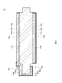
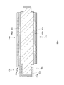
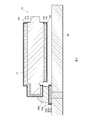
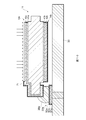
- FIG. 1 It is an exploded perspective view which shows schematic structure of the crystal oscillator which concerns on 1st Embodiment. It is sectional drawing which shows schematic the structure of the cross section of the crystal oscillator shown in FIG. 1 along the line II-II. It is sectional drawing which shows schematic structure of the crystal vibration element shown in FIG. It is a flowchart which shows a part of the manufacturing method of the crystal vibration element which concerns on 1st Embodiment. It is sectional drawing which shows typically the process of forming the base layer and the surface layer on a crystal piece. It is sectional drawing which shows typically the process of patterning an electrode. It is sectional drawing which shows the diffusion process of chromium schematicly.
- Each drawing consists of a first direction D1, a second direction D2, and a third direction D3 for convenience, in order to clarify the relationship between the drawings and to help understand the positional relationship of each member.
- a Cartesian coordinate system may be attached.
- the first direction D1, the second direction D2, and the third direction D3 mean the three reference directions shown in FIG. 1, respectively, in the direction of the arrow (positive direction) and the direction opposite to the arrow (negative direction). )including.
- a piezoelectric vibrator piezoelectric Resonator Unit
- a crystal oscillator Quadrature Crystal Resonator Unit
- a crystal vibration element Quadrature Crystal Resonator
- the crystal vibrating element uses a crystal piece (Quartz Crystal Element) as a piezoelectric material that vibrates according to an applied voltage.
- a crystal oscillator corresponds to an example of a piezoelectric vibrator
- a crystal vibrating element corresponds to an example of a piezoelectric vibrating element
- a crystal piece corresponds to an example of a piezoelectric piece.
- the piezoelectric piece according to the embodiment of the present invention is not limited to the crystal piece.
- the piezoelectric piece may be formed of any piezoelectric material such as a piezoelectric single crystal, a piezoelectric ceramic, a piezoelectric thin film, or a piezoelectric polymer membrane.
- the piezoelectric single crystal can include lithium niobate (LiNbO 3 ).
- the piezoelectric ceramic is barium titanate (BaTiO 3), lead titanate (PbTiO 3), lead zirconate titanate (Pb (Zr x Ti 1- x) O 3; PZT), aluminum nitride (AlN), Lithium niobate (LiNbO 3 ), lithium metaniobate (LiNb 2 O 6 ), bismuth titanate (Bi 4 Ti 3 O 12 ) lithium tantalate (LiTaO 3 ), lithium tetraborate (Li 2 B 4 O 7 ), Langasite (La 3 Ga 5 SiO 14 ), tantalate pentoxide (Ta 2 O 5 ) and the like can be mentioned.
- Examples of the piezoelectric thin film include those obtained by forming the above-mentioned piezoelectric ceramic on a substrate such as quartz or sapphire by a sputtering method or the like.
- Examples of the piezoelectric polymer film include polylactic acid (PLA), polyvinylidene fluoride (PVDF), vinylidene fluoride / ethylene trifluoride copolymer (P (VDF / TrFE)), and the like.
- PVA polylactic acid
- PVDF polyvinylidene fluoride
- PVDF vinylidene fluoride / ethylene trifluoride copolymer
- the above-mentioned various piezoelectric materials may be used by being laminated with each other, or may be laminated with a member other than the piezoelectric material.
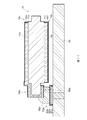
- FIG. 1 is an exploded perspective view schematically showing the configuration of the crystal oscillator according to the first embodiment.
- FIG. 2 is a cross-sectional view schematically showing the configuration of the cross section of the crystal oscillator shown in FIG. 1 along the line II-II.
- FIG. 3 is a cross-sectional view schematically showing the configuration of the crystal vibrating element shown in FIG.
- the crystal oscillator 1 includes a crystal vibrating element 10, a lid member 20, a base member 30, and a joining member 40.
- the base member 30 and the lid member 20 are cages for accommodating the crystal vibrating element 10.
- the lid member 20 is formed in a concave shape.
- the lid member 20 is formed in a concave shape having an opening for accommodating the crystal vibration element 10 on the base member 30 side.
- the base member 30 is formed in a flat plate shape.
- the shapes of the lid member 20 and the base member 30 are not limited to the above.
- the shape of the lid member 20 is a flat plate shape
- the shape of the base member 30 is a concave shape having an opening on the lid member 20 side. May be good.
- the lid member 20 and the base member 30 may both have a concave shape having an opening on the side facing each other.
- the crystal vibrating element 10 is an element that vibrates a crystal by a piezoelectric effect and converts electrical energy and mechanical energy.
- the crystal vibrating element 10 includes a flaky crystal piece 11, a pair of first excitation electrodes 14a and a second excitation electrode 14b, a pair of first extraction electrodes 15a and a second extraction electrode 15b, and a pair of first connection electrodes.
- a 16a and a second connection electrode 16b are provided.
- the crystal piece 11 has a front surface 11A and a back surface 11B facing each other.
- the surface 11A is located on the side opposite to the side facing the base member 30, that is, the side facing the top surface portion 21 of the lid member 20, which will be described later.
- the back surface 11B is located on the side facing the base member 30.
- the crystal piece 11 is, for example, an AT-cut type crystal piece.
- the AT-cut type crystal piece 11 is a plane parallel to a plane specified by the X-axis and the Z'axis in a Cartesian coordinate system consisting of an X-axis, a Y'axis, and a Z'axis that intersect each other (hereinafter, "XZ". It is called a'plane'.
- XZ X-axis
- Y'axis a Z'axis that intersect each other
- the AT-cut type crystal piece 11 is formed by etching a crystal substrate (for example, a crystal wafer) obtained by cutting and polishing an ingot of an artificial crystal (Synthetic Quartz Crystal).
- the Y'axis and the Z'axis are axes obtained by rotating the Y axis and the Z axis around the X axis in the direction of the Y axis to the Z axis by 35 degrees 15 minutes ⁇ 1 minute 30 seconds, respectively.
- the X-axis, Y-axis, and Z-axis are crystallographic axes of quartz.
- the X-axis corresponds to the electric axis (polar axis)
- the Y-axis corresponds to the mechanical axis
- the Z-axis corresponds to the optical axis.
- the crystal vibrating element 10 using the AT-cut type crystal piece 11 has high frequency stability in a wide temperature range.
- the thickness slip vibration mode Thiickness Shear Vibration Mode
- the rotation angles of the Y'axis and the Z'axis of the AT-cut type crystal piece 11 may be tilted in the range of 35 degrees 15 minutes to ⁇ 5 degrees or more and 15 degrees or less.
- a different cut other than the AT cut for example, BT cut
- the crystal vibrating element 10 has an X-axis parallel to the first direction D1, a Z'axis parallel to the second direction D2, and a Y'axis parallel to the third direction D3. It is arranged like this.
- the directions parallel to the X-axis, the Y'axis, and the Z'axis are referred to as the X-axis direction, the Y'axis direction, and the Z'axis direction, respectively. That is, the X-axis direction corresponds to the first direction D1, the Z'axis direction corresponds to the second direction D2, and the Y'axis corresponds to the third direction D3.
- the + X-axis direction is the positive direction of the first direction D1
- the ⁇ X-axis direction is the negative direction of the first direction D1.
- the + Y'axis direction is the positive direction of the third direction D3
- the ⁇ Y'axis direction is the negative direction of the third direction D3.
- the + Z'axis direction is the positive direction of the second direction D2
- the ⁇ Z'axis direction is the negative direction of the second direction D2. Therefore, the main surface of the AT-cut type crystal piece 11 is parallel to the D1D2 surface specified by the first direction D1 and the second direction D2.
- the AT-cut type crystal piece 11 is parallel to the long side direction in which the long side parallel to the X-axis direction extends, the short side direction in which the short side parallel to the Z'axis direction extends, and the Y'axis direction. It is a plate shape having a thickness direction in which a large thickness extends.
- the crystal piece 11 has a rectangular shape when the surface 11A is viewed in a plan view, and includes an excitation unit 17 located at the center and contributing to excitation, and peripheral portions 18 and 19 adjacent to the excitation unit 17.
- the excitation portion 17 and the peripheral portions 18 and 19 are formed in a band shape from one end to the other end facing each other in the Z'axis direction of the crystal piece 11, respectively.
- the peripheral portion 18 is located on the ⁇ X axis direction side when viewed from the excitation unit 17, and the peripheral portion 19 is located on the + X axis direction side when viewed from the excitation unit 17.
- the shape of the exciting portion 17 is not limited to a band shape formed over the entire width from one end to the other end facing each other in the Z'axis direction.
- the excitation unit 17 may have an island shape that is adjacent to the peripheral portion in the Z'axis direction and is surrounded by the peripheral portion.
- the shapes of the peripheral portions 18 and 19 are not limited to the strip shape formed over the entire width from one end to the other end facing each other in the Z'axis direction.
- the peripheral portion may be formed in a frame shape surrounding the excitation portion.
- the exciting portion 17 has a main surface 17A
- the peripheral portion 18 has a main surface 18A
- the peripheral portion 19 has a main surface 19A.
- the exciting portion 17 has a main surface 17B
- the peripheral portion 18 has a main surface 18B
- the peripheral portion 19 has a main surface 19B.
- the exciting part 17 is thicker than the peripheral parts 18 and 19.
- the crystal piece 11 has a double-sided mesa type structure. As a result, vibration leakage from the excitation unit 17 can be suppressed.
- the excitation portion 17 protrudes from the peripheral portions 18 and 19 along the Y'axis direction on both the front surface 11A side and the back surface 11B side of the crystal piece 11.
- a step is formed at the boundary between the main surface 17A of the excitation portion 17 and the main surface 18A of the peripheral portion 18, and the main surface 17A of the excitation portion 17 and the main surface of the peripheral portion 19 are formed.
- a step is formed at the boundary with 19A.
- a step is formed at the boundary between the main surface 17B of the excitation portion 17 and the main surface 18B of the peripheral portion 18, and the main surface 17B of the excitation portion 17 and the main surface of the peripheral portion 19 are formed.
- a step is formed at the boundary with 19B.
- the shape of the step at the boundary between the exciting portion 17 and the peripheral portions 18 and 19 is, for example, tapered, but may be another shape such as a multi-stage shape.
- the shape of the crystal piece 11 is not limited to the above, and for example, the peripheral portion 19 may be omitted. Further, the crystal piece 11 is not limited to the double-sided mesa type structure, and the single-sided mesa type structure in which the excitation portion 17 protrudes from the peripheral portions 18 and 19 only on one side of the front surface 11A and the back surface 11B and the excitation portion 17 It may have an inverted mesa type structure thinner than the peripheral portions 18 and 19.
- the crystal piece 11 may have a convex structure or a beher type structure in which the amount of change in thickness between the excitation portion 17 and the peripheral portions 18 and 19 continuously changes.
- the shape of the crystal piece 11 is not limited to a plate shape, and may be, for example, a tuning fork shape having a base portion and a vibrating arm portion extending in parallel from the base portion.
- the first excitation electrode 14a is provided on the main surface 17A of the excitation portion 17. Further, the second excitation electrode 14b is provided on the main surface 17B of the excitation portion 17. In other words, the first excitation electrode 14a is provided on the side of the lid member 20, and the second excitation electrode 14b is provided on the side of the base member 30.
- the first excitation electrode 14a and the second excitation electrode 14b face each other with the crystal piece 11 interposed therebetween in the third direction D3.
- the first excitation electrode 14a and the second excitation electrode 14b are arranged so that substantially the entire surface of the XZ'is overlapped with each other.
- the first excitation electrode 14a and the second excitation electrode 14b each have a long side parallel to the X-axis direction, a short side parallel to the Z'axis direction, and a thickness parallel to the Y'axis direction. ..
- the first excitation electrode 14a has a base layer 41a and a surface layer 42a, and the base layer 41a and the surface layer 42a are laminated in this order when viewed from the crystal piece 11.
- the base layer 41a is provided with a material having a higher adhesion to the crystal piece 11 than the material of the surface layer 42a, and contains chromium (Cr) as a main component.
- the surface layer 42a is provided with a material having higher chemical stability than the material of the base layer 41a, and contains gold (Au) as a main component. Chromium is present on the surface of the first excitation electrode 14a. Although not shown in FIG. 3, chromium derived from the base layer 41a is diffused inside the surface layer 42a of the first excitation electrode 14a.
- the second excitation electrode 14b has a base layer 41b containing chromium as a main component and a surface layer 42b containing gold as a main component. Chromium is present on the surface of the second excitation electrode 14b. Similar to the first excitation electrode 14a, chromium derived from the base layer 41b is diffused inside the surface layer 42b of the second excitation electrode 14b. In the example shown in FIG. 3, the thickness of at least a part of the first excitation electrode 14a is thinner than the thickness of the second excitation electrode 14b. This is because a part of the surface layer 42a of the first excitation electrode 14a is trimmed for the purpose of frequency adjustment.
- the film thickness of the base layer 41b of the second excitation electrode 14b is, for example, the same as the film thickness of the base layer 41a of the first excitation electrode 14a, but may be different.
- the film thickness of the surface layer 42b of the second excitation electrode 14b is larger than, for example, the film thickness of the surface layer 42a of the first excitation electrode 14a, but may be the same or less.
- substantially all of the chromium on the surfaces of the first excitation electrode 14a and the second excitation electrode 14b is oxidized and exists as chromium oxide.
- chromium oxide 43a is formed on substantially the entire surface of the first excitation electrode 14a
- chromium oxide 43b is formed on substantially the entire surface of the second excitation electrode 14b.
- Cr 2 O 3 is more than CrO, for example, almost all are Cr 2 O 3 .
- More chromium oxide is formed on the surface of the surface layer 42b of the second excitation electrode 14b than on the surface of the surface layer 42a of the first excitation electrode 14a.
- the comparison of the amount of chromium oxide on each surface of the surface layers 42a and 42b is made by, for example, the amount of chromium oxide per unit area when the surface layers 42a and 42b are viewed in a plan view.
- the amount of chromium oxide formed on the surfaces of the surface layers 42a and 42b of the first excitation electrode 14a and the second excitation electrode 14b is, for example, EDX (energy dispersive X-ray analysis method) or WDX (wavelength dispersive X). It is measured by line analysis method).
- the oxidation state of the chromium i.e., the ratio of CrO and Cr 2 O 3 is measured, for example, such as by XPS (X-ray photoelectron spectroscopy).
- the analysis method is not limited to the above, and the same applies to qualitative quantitative analysis methods such as secondary ion mass spectrometry, electron beam microanalysis, Auger electron spectroscopy, and fluorescence X-ray analysis. It is possible to perform an analysis. Further, the amount of chromium oxide and the oxidation state of chromium may be determined using the results measured at one location, but preferably, the average value of the results measured at a plurality of locations, for example, 2 to 10 locations is used. May be decided.
- the size of the measurement region for determining the amount of chromium oxide and the oxidation state of chromium is not particularly limited, and may be a range that can be set when using the above-mentioned analyzer.
- the measurement area at one location is also described as the measurement area at one location.
- the chromium oxide 43a is drawn in the form of a thin film continuously extending along the main surface 17A, but the chromium oxide 43a is drawn. Is not always formed in a thin film shape so as to cover the first excitation electrode 14a. Chromium oxide 43a may be mottled on the surface of the surface layer 42a of the first excitation electrode 14a. Similarly, chromium oxide 43b may be mottled on the surface of the surface layer 42b of the second excitation electrode 14b.
- the first extraction electrode 15a is provided on the main surface 18A of the peripheral portion 18, and electrically connects the first excitation electrode 14a and the first connection electrode 16a.
- the second extraction electrode 15b is provided on the main surface 18B of the peripheral portion 18, and electrically connects the second excitation electrode 14b and the second connection electrode 16b.
- the first extraction electrode 15a and the second extraction electrode 15b are also formed at a step at the boundary between the peripheral portion 18 and the excitation portion 17, respectively. From the viewpoint of reducing stray capacitance, when the surface 11A of the crystal piece 11 is viewed in a plan view, the first extraction electrode 15a and the second extraction electrode 15b do not overlap and are separated from each other.
- the first connection electrode 16a and the second connection electrode 16b are provided on the main surface 18B of the peripheral portion 18.
- the first excitation electrode 14a, the first extraction electrode 15a, and the first connection electrode 16a are integrally formed. The same applies to the second excitation electrode 14b, the second extraction electrode 15b, and the second connection electrode 16b.
- the first extraction electrode 15a has a base layer 51a and a surface layer 52a
- the first connection electrode 16a has a base layer 61a and a surface layer 62a.
- the base layers 51a and 61a of the first extraction electrode 15a and the first connection electrode 16a are integrally formed of the same material as the base layer 41a of the first excitation electrode 14a.
- the surface layers 52a and 62a of the first extraction electrode 15a and the first connection electrode 16a are integrally formed of the same material as the surface layer 42a of the first excitation electrode 14a.
- chromium oxide 53a is formed on the surface of the first extraction electrode 15a, and chromium derived from the base layer 51a diffuses inside the surface layer 52a of the first extraction electrode 15a.
- Chromium oxide 63a is also formed on the surface of the first connection electrode 16a, and chromium derived from the base layer 61a is diffused inside the surface layer 62a of the first connection electrode 16a.
- the second extraction electrode 15b and the second connection electrode 16b also have a base layer and a surface layer like the second excitation electrode 14b. Chromium oxide is formed on the surfaces of the second extraction electrode 15b and the second connection electrode 16b.
- the thickness of at least a part of the first excitation electrode 14a may be thinner than the thickness of the first extraction electrode 15a.
- the thickness of the surface layer 42a of the first excitation electrode 14a in the central portion of the excitation portion 17 may be thinner than the thickness of the surface layer 52a of the first extraction electrode 15a in the peripheral portion 18.
- more chromium oxide is formed on the surfaces of the first extraction electrode 15a and the first connection electrode 16a than on the surface of the first excitation electrode 14a.
- the lid member 20 has a concave shape, specifically, a concave shape that opens toward the main surface 32A of the base member 30.
- the lid member 20 is joined to the base member 30 to form an internal space 26 in which the crystal vibrating element 10 is housed with the base member 30.
- the shape of the lid member 20 is not particularly limited as long as it can accommodate the crystal vibrating element 10.
- the lid member 20 has a rectangular shape when viewed in a plan view from the normal direction of the main surface of the top surface portion 21. There is.
- the lid member 20 has, for example, a long side parallel to the first direction D1, a short side parallel to the second direction D2, and a height parallel to the third direction D3.
- the material of the lid member 20 is not particularly limited, but is made of a conductive material such as metal. Since the lid member 20 is made of a conductive material, the lid member 20 is provided with an electromagnetic shield function that reduces the ingress and egress of electromagnetic waves into the internal space 26.
- the lid member 20 has an inner surface 24 and an outer surface 25.
- the inner surface 24 is a surface on the inner space 26 side
- the outer surface 25 is a surface on the opposite side to the inner surface 24.
- the lid member 20 has a flat top surface portion 21 and a side wall portion 22 that is connected to the outer edge of the top surface portion 21 and extends in a direction intersecting the main surface of the top surface portion 21. ..
- the lid member 20 has a facing surface 23 facing the base member 30 at the concave opening end portion (the end portion of the side wall portion 22 on the side closer to the base member 30).
- the facing surface 23 extends in a frame shape so as to surround the crystal vibrating element 10.
- the base member 30 holds the crystal vibrating element 10 in an excitable manner.
- the base member 30 has a flat plate shape and has a long side parallel to the first direction D1 direction, a short side parallel to the second direction D2, and a thickness parallel to the third direction D3.
- the base member 30 has a base 31.
- the substrate 31 has a main surface 32A (front surface) and a main surface 32B (back surface) facing each other.
- the substrate 31 is a sintered material such as an insulating ceramic (alumina).
- the substrate 31 is preferably made of a heat resistant material.
- a pair of first electrode pads 33a and second electrode pads 33b are provided on the main surface 32A of the base member 30.
- the main surface 32B of the base member 30 is provided with a first external electrode 35a, a second external electrode 35b, a third external electrode 35c, and a fourth external electrode 35d.
- the first electrode pad 33a and the second electrode pad 33b are terminals for electrically connecting the base member 30 and the crystal vibrating element 10.
- the first external electrode 35a and the second external electrode 35b are terminals for electrically connecting an external circuit board (not shown) and the crystal oscillator 1.
- the third external electrode 35c and the fourth external electrode 35d are dummy electrodes to which electric signals and the like are not input / output, but may be ground electrodes that ground the lid member 20 to improve the electromagnetic shield function of the lid member 20.
- the third external electrode 35c and the fourth external electrode 35d may be omitted.
- the first electrode pad 33a and the second electrode pad 33b are lined up along the second direction D2.
- the first external electrode 35a and the fourth external electrode 35d are arranged along the first direction D1.
- the second external electrode 35b and the third external electrode 35c are arranged along the first direction D1.
- the first electrode pad 33a is electrically connected to the first external electrode 35a via the first via electrode 34a extending in the third direction D3.
- the second electrode pad 33b is electrically connected to the second external electrode 35b via the second via electrode 34b extending in the third direction D3.
- the first via electrode 34a and the second via electrode 34b are formed in a via hole that penetrates the substrate 31 in the third direction D3.
- a pair of first conductive holding member 36a and second conductive holding member 36b are provided on the main surface 32A side of the base member 30.
- the first conductive holding member 36a is provided on the first electrode pad 33a
- the second conductive holding member 36b is provided on the second electrode pad 33b.
- the first conductive holding member 36a and the second conductive holding member 36b mount the crystal vibrating element 10 on the base member 30, and electrically connect the crystal vibrating element 10 and the base member 30.
- the first conductive holding member 36a is joined to the first connection electrode 16a of the crystal vibrating element 10, and the first electrode pad 33a and the first connection electrode 16a are electrically connected.
- the second conductive holding member 36b is joined to the second connection electrode 16b of the crystal vibrating element 10, and the second electrode pad 33b and the second connection electrode 16b are electrically connected.
- the first conductive holding member 36a and the second conductive holding member 36b hold the crystal vibrating element 10 at intervals from the base member 30 so that the exciting portion 17 can be excited.
- the first conductive holding member 36a and the second conductive holding member 36b are conductive adhesives containing, for example, a thermosetting resin containing a silicone-based resin as a main component, an ultraviolet curable resin, and the like, and imparting conductivity to the adhesive. Contains additives such as conductive particles for.
- conductive particles for example, conductive particles containing silver (Ag) are used.
- the main agent of the conductive adhesive may be an epoxy resin or the like.
- the first conductive holding member 36a and the second conductive holding member 36b are coated with the uncured conductive adhesive paste which is a precursor, and then the conductive adhesive is subjected to a chemical reaction caused by heating, ultraviolet irradiation, or the like. It is provided by curing the paste. Further, a filler may be added to the adhesive for the purpose of increasing the strength or maintaining the distance between the base member 30 and the crystal vibrating element 10.
- the first conductive holding member 36a and the second conductive holding member 36b may be provided by soldering.
- the joining member 40 is provided over the entire circumference of the lid member 20 and the base member 30. Specifically, the joining member 40 has a rectangular frame shape when the main surface 32A is viewed in a plan view. Further, the first electrode pad 33a and the second electrode pad 33b are arranged inside the joining member 40, and the joining member 40 is provided so as to surround the crystal vibration element 10. The joining member 40 is sandwiched between the facing surface 23 of the side wall portion 22 of the lid member 20 and the first main surface 32A of the base member 30.
- the joining member 40 is provided, for example, with a resin-based adhesive.
- the joining member 40 may be provided with a glass-based adhesive, an Au—Sn alloy-based metal solder, or the like.
- the joining member 40 When the joining member 40 is provided by metal solder, a metallized layer may be provided on the base member 30 from the viewpoint of improving the adhesion to the joining member 40.
- the joining member 40 is provided in a frame shape continuous in the circumferential direction, but may be provided discontinuously in the circumferential direction.
- FIG. 4 is a flowchart schematically showing a part of the method for manufacturing a crystal oscillator according to the first embodiment.
- 5 to 12 are diagrams for explaining a method of manufacturing a crystal oscillator. Specifically, FIG. 5 is a cross-sectional view schematically showing a step of forming a base layer and a surface layer on a crystal piece.
- FIG. 6 is a cross-sectional view schematically showing a step of patterning the electrodes.
- FIG. 7 is a cross-sectional view schematically showing a chromium diffusion process.
- FIG. 5 is a cross-sectional view schematically showing a step of forming a base layer and a surface layer on a crystal piece.
- FIG. 6 is a cross-sectional view schematically showing a step of patterning the electrodes.
- FIG. 7 is a cross-sectional view schematically showing a chromium diffusion process.
- FIG. 8 is a cross-sectional view schematically showing an oxidation step of oxidizing chromium on the surface of the electrode.
- FIG. 9 is a cross-sectional view schematically showing a mounting process for mounting the crystal vibration element on the base member.
- FIG. 10 is a cross-sectional view schematically showing a frequency adjustment process for trimming the second excitation electrode.
- FIG. 11 is a cross-sectional view schematically showing an oxidation step of oxidizing chromium exposed on the surface of the excitation electrode.
- FIG. 12 is a cross-sectional view schematically showing a joining process of joining the lid member to the base member.
- a crystal piece is prepared (S101).
- a crystal substrate was cut out from a single crystal of an artificial quartz so that the XZ'plane was the main surface, a part of the crystal substrate was removed by wet etching using a photolithography method, and the XZ'plane was viewed in a plan view.
- the contour of the crystal piece 11 is formed.
- a part of the peripheral portions 18 and 19 of the crystal piece 11 is removed by wet etching to form a double-sided mesa-shaped structure.
- an electrode forming step of providing an electrode on the crystal piece 11 is carried out.
- the "electrode” is used as a general term for various electrodes provided in the crystal vibrating element, and specifically, the first and second excitation electrodes, the first and second extraction electrodes, and the first and first electrodes. 2 Refers to the connection electrode.
- a base layer is first provided (S102), and then a surface layer is provided (S103). Then, the base layer and the surface layer are etched (S104).
- the base layer 41 is provided so as to wrap the crystal piece 11 by depositing a metal material containing Cr on the surface of the crystal piece 11 by sputtering, for example.
- the base layer 41 is formed so as to have a thickness of, for example, 1 nm or more and 20 nm or less. By setting the thickness to 1 nm or more, it is possible to suppress a decrease in the adhesion to the crystal piece 11. Further, by setting the thickness to 20 nm or less, deterioration of vibration characteristics with time can be suppressed.
- the surface layer 42 is provided so as to wrap the base layer 41 by depositing, for example, a metal material containing Au on the surface of the base layer 41 by sputtering.
- the base layer 41 is formed so as to have a thickness of, for example, 1 nm or more and 500 nm or less. By setting the thickness to 1 nm or more, oxidation of the base layer 41 can be suppressed. Further, by setting the thickness to 500 nm or less, the amount of Au used can be reduced, and the time required for forming the surface layer 42 can be shortened.
- the surface layer 42 on the surface 11A side of the crystal piece 11 is more than the surface layer 42 on the back surface 11B side so that the surface layer 42 on the main surface 17A side is completely removed and the base layer 41 is not exposed in the frequency adjustment step described later. May be thickly formed.
- the film forming method of the base layer 41 and the surface layer 42 is not limited to sputtering, and may be appropriately selected from various vapor deposition methods such as PVD (Physical Vapor Deposition) and CVD (Chemical Vapor Deposition). Further, the base layer 41 and the surface layer 42 may be formed by a film forming method other than the vapor deposition method such as a printing method or a plating method.
- the outer shape of the electrode is formed by the step S104 of etching the base layer 41 and the surface layer 42. Specifically, the base layer 41 and the surface layer 42 other than the portions corresponding to the first and second excitation electrodes 14a and 14b, the first and second extraction electrodes 15a and 15b, and the first and second connection electrodes 16a and 16b are provided. , Removed by wet etching using a photolithography method.
- the electrode forming step is not limited to the above.
- the electrode is formed by forming a base layer and a surface layer on the patterned photoresist and removing unnecessary portions together with the photoresist, so-called lift-off. It may be formed.
- This step S105 is an electrode diffusion step of diffusing chromium into the surface layer of the electrode, and corresponds to an excitation electrode diffusion step, an extraction electrode diffusion step, and a connection electrode diffusion step.
- the chromium 70 contained in the base layer 41a diffuses into the surface layer 42a.
- the chromium 70 that has reached the side of the surface layer 42a opposite to the base layer 41a side is deposited on the surface of the surface layer 42a. Diffusion proceeds until the amount of chromium 70 on the surface of the surface layer 42a is greater than the amount of chromium 70 inside the surface layer 42a.
- the amount of chromium 70 on the surface and inside of the surface layer 42a is compared, for example, by the amount of chromium 70 per unit area or the amount of chromium 70 per unit volume in a cross-sectional view as shown in FIG. 7.
- chromium is diffused in the second excitation electrodes 14b, the first and second extraction electrodes 15a and 15b, and the first and second connection electrodes 16a and 16b. Diffusion of chromium 70 is promoted, for example, by heating in vacuum or in an atmosphere of an inert gas.
- the chromium on the electrode surface is oxidized (S106).
- This step S106 corresponds to the first oxidation step and the second oxidation step.
- the chromium 70 exposed on the surfaces of the first and second excitation electrodes 14a and 14b, the first and second extraction electrodes 15a and 15b, and the first and second connection electrodes 16a and 16b is oxygenated. Heated inside to form chromium oxide 71.
- Chromium oxide 71 is preferably Cr 2 O 3 , but may contain CrO at this stage.
- the crystal vibration element is mounted on the base member (S107).
- This step S107 corresponds to the mounting step.
- the uncured first and second conductive holding members 36a and 36b are coated on the first and second electrode pads 33a and 33b of the base member 30, and the uncured first and second conductive holding members are coated.
- the crystal vibration element 10 is allowed to stand on the 36a and 36b to cure the first and second conductive holding members 36a and 36b.
- the first and second conductive holding members 36a and 36b are thermosetting resins
- the first and second excitation electrodes 14a and 14b are heated by heating when the first and second conductive holding members 36a and 36b are cured.
- the chromium exposed on the surface of the surface may be oxidized.
- a step of providing the base member 30 is carried out before the mounting step S107.
- the pad forming step of providing the electrode pad 33a includes a step of providing the base layer 91a and a surface.
- It may have a step of providing the layer 92a, a step of diffusing chromium in the surface layer 92a, and a step of oxidizing the chromium exposed on the surface of the surface layer 92a.
- chromium oxide 93a is formed on the surface of the surface layer 92a of the electrode pad 33a. Since the chromium oxide 93a formed on the surface of the electrode pad 33a is sufficiently thin, the electrical connection between the crystal vibrating element 10 and the base member 30 is not hindered.
- the first excitation electrode is trimmed (S108).
- This step S108 corresponds to the frequency adjustment step.
- the mass of the excitation unit 17 is changed, and the resonance frequency of the crystal vibration element 10 is adjusted.
- the chromium oxide 71 formed on the surface of the first excitation electrode 14a is also removed. Less chromium is exposed on the trimmed surface of the surface layer 42a than on the untrimmed surface of the surface layer 42a. This is because, as described above, the amount of chromium inside the surface layer 42a is less than the amount of chromium on the surface. Trimming is performed by, for example, dry etching by irradiating an argon (Ar) ion beam. Since the ion beam can irradiate a wide range, it has excellent processing efficiency.
- Ar argon
- This step S109 corresponds to an oxidation step.
- the chromium exposed on the surface of the surface layer 42a of the first excitation electrode 14a is oxidized.
- This step S109 corresponds to a step of forming chromium oxide on the surface of the surface layer 42a of the first excitation electrode 14a. Since the amount of chromium exposed on the surface of the trimmed first excitation electrode 14a is less than the amount of chromium exposed on the surface of the untrimmed second excitation electrode 14b, it is formed on the surface of the second excitation electrode 14b.
- a smaller amount of chromium oxide 43b than the amount of chromium oxide 43b is formed on the surface of the first excitation electrode 14a.
- the chromium oxide 43a formed on the surface of the first excitation electrode 14a is Cr 2 O 3 .
- Cr or CrO remains on the surfaces of the second excitation electrode 14b, the first connection electrode 16a and the second connection electrode 16b, it is desirable to change the Cr 2 O 3 to Cr 2 O 3 in this step S109.
- the oxidation conditions such as the heating temperature and the heating time may be the same as those of the oxidation step of S106 that is performed prior to the step.
- the oxidation step of S109 may have different oxidation conditions to promote oxidation than the oxidation step of S106.
- the oxidation step of S109 may have a higher heating temperature than the oxidation step of S106, or the heating time may be longer.
- This step S110 corresponds to a joining step.
- the uncured joint member 40 is attached to the open end of the lid member 20, and the uncured joint member 40 is cured while being sandwiched between the lid member 20 and the base member 30.
- the manufacturing method of the crystal vibrating element 10 is not limited to the above.
- the diffusion step S105 may be carried out before the step S104 for etching the base layer and the surface layer
- the oxidation step S106 may be carried out before the step S104 for etching the base layer and the surface layer.
- the diffusion step S105 and the oxidation step S106 may be carried out between the mounting step S107 and the frequency adjustment step S108. Further, the oxidation step S106 may be omitted.
- the surface of the surface layer 42b of the second excitation electrode 14b has more chromium oxide than the surface of the surface layer 42a of the first excitation electrode 14a. Is formed. According to this, since the organic substance is less likely to be adsorbed on the surface of chromium oxide than the surface of the metal, the organic substance evaporated from the first and second conductive holding members 36a and 36b is transferred to the first and second excitation electrodes 14a and 14b. Accumulation can be suppressed. In other words, the antifouling property of the first and second excitation electrodes 14a and 14b is improved.
- the mass change of the first and second excitation electrodes 14a and 14b can be suppressed, and the change of the resonance frequency of the crystal oscillator 1 with time can be reduced. Therefore, the reliability of the crystal oscillator 1 is improved.
- the antifouling property of the second excitation electrode 14b which is closer to the contamination source than the first excitation electrode 14a, is higher than the antifouling property of the first excitation electrode 14a. Therefore, it is possible to more effectively reduce the change in the resonance frequency of the crystal oscillator 1 with time.
- FIG. 13 is a cross-sectional view schematically showing the configuration of the crystal oscillator according to the second embodiment.
- the crystal oscillator 200 according to the second embodiment is the same as the crystal oscillator 1 according to the first embodiment, that is, the crystal vibration element 210, the lid member 220, the base member 230, the first conductivity holding member 236a, and the joining member. It is equipped with 240.
- the crystal vibration element 210 has a first excitation electrode 214a and a second excitation electrode 214b.
- the first excitation electrode 214a has a base layer 241a and a surface layer 242a, and chromium oxide 243a is formed on the surface of the first excitation electrode 214a.
- the second excitation electrode 214b has a base layer 241b and a surface layer 242b, and more chromium oxide 243a is formed on the surface of the second excitation electrode 214b than on the surface of the first excitation electrode 214a.
- the difference from the first embodiment of the second embodiment is that a surface layer thicker than that of the second excitation electrode 214b is formed on the first excitation electrode 214a in the step of providing the surface layer.
- the thickness T1 of the surface layer 242a of the first excitation electrode 214a is larger than the thickness T2 of the surface layer 242b of the second excitation electrode 214b.
- the crystal vibrating element 210 is mounted in a direction in which the excitation electrode 214b having the thinner surface layer 242b is arranged on the side of the base member 230.
- the chromium diffusion path of the first excitation electrode 214a is longer than the chromium diffusion path of the second excitation electrode 214b. Therefore, in the diffusion step, more chromium is deposited on the surface of the surface layer 242b of the second excitation electrode 214b than on the surface of the surface layer 242a of the first excitation electrode 214a. Therefore, more chromium oxide 243b can be formed than chromium oxide 243a without forming a surface with a small amount of chromium exposed by the frequency adjustment step on the first excitation electrode 214a.
- a step of forming a piezoelectric vibrating element having a piezoelectric piece and a pair of excitation electrodes facing each other with the piezoelectric piece interposed therebetween, and each of the pair of excitation electrodes has a base layer and a surface.
- the step of forming the piezoelectric vibrating element including the layer and the base layer containing chromium, the step of mounting the piezoelectric vibrating element on the base member by the conductive holding member, and the step of mounting the piezoelectric vibrating element on the base member so that the piezoelectric vibrating element is located between the base member.
- the excitation electrode on the base member side Provided is a method for manufacturing a piezoelectric vibrator, which has a larger amount of chromium oxide on the surface of the surface layer than the excitation electrode on the side of the lid member. According to this, since the organic substance is less likely to be adsorbed on the surface of chromium oxide than the surface of metal, it is possible to suppress the deposition of the organic substance evaporated from the conductive holding member on the pair of excitation electrodes. In other words, the antifouling property of the pair of excitation electrodes is improved.
- the change in mass of the pair of excitation electrodes can be suppressed, and the change in the resonance frequency of the piezoelectric vibrator with time can be reduced.
- the antifouling property of the excitation electrode on the side of the base member close to the contamination source becomes higher than the antifouling property of the excitation electrode on the side of the lid member, so that the resonance frequency of the piezoelectric vibrator The change over time can be reduced more effectively.
- the chromium oxide is Cr 2 O 3 . According to this, the mass change of the pair of excitation electrodes by chemical change to Cr 2 O 3 from CrO can be suppressed.
- the step of providing the lid member includes a step of joining the lid member to the base member by the joining member so as to accommodate the piezoelectric vibrating element.
- a lid member is provided after forming chromium oxide. According to this, even if a joining member existing in a larger amount than the conductive holding member becomes a pollution source, the mass change of the excitation electrode, particularly the mass change of the second excitation electrode can be suppressed.
- One aspect further includes a step of trimming the excitation electrode on the side opposite to the base member of the pair of excitation electrodes after mounting the piezoelectric vibration element to adjust the frequency of the piezoelectric vibration element.
- chromium oxide is formed after adjusting the frequency of the piezoelectric vibrating element.
- a step of diffusing chromium from the base layer to the surface layer is further included, and after the chromium is diffused, the frequency of the piezoelectric vibrating element is adjusted. According to this, by trimming, a surface having less chromium than before trimming can be formed on the surface layer of the excitation electrode on the side of the lid member.
- the method for manufacturing the piezoelectric vibrator includes a first oxidation step of oxidizing the chromium diffused from the base layer to the surface layer after diffusing the chromium and before adjusting the frequency of the piezoelectric vibrating element. Including further.
- the step of forming the piezoelectric vibrating element includes a step of forming the surface layer of one of the pair of excitation electrodes to be thicker than the surface layer of the other excitation electrode, and the piezoelectric vibrating element is used as a base member.
- the mounting step includes a step of mounting the piezoelectric vibrating element in the direction in which the thinner surface layer of the pair of excitation electrodes is arranged on the side of the base member.
- the piezoelectric vibrating element further has a pair of connecting electrodes provided on the piezoelectric piece, and each of the pair of connecting electrodes includes a base layer containing chromium and a surface layer, and the pair of connecting electrodes. Each further comprises a second oxidation step of oxidizing the chromium diffused from the base layer to the surface layer.
- the base member is flat and the lid member is concave with an opening for accommodating the piezoelectric vibrating element. According to this, since the joining member is arranged closer to the excitation electrode on the side of the base member than the excitation electrode on the side of the lid member, the excitation electrode on the side of the base member is further closer than the excitation electrode on the side of the lid member. Although the environment is easily contaminated, the mass change of the excitation electrode on the base member side can be suppressed.
- the piezoelectric vibrating element is a crystal vibrating element.
- the present invention has a base member, a first excitation electrode and a second excitation electrode facing each other with the piezoelectric piece and the piezoelectric piece interposed therebetween, and the second excitation electrode faces the base member.
- a lid member provided so that a piezoelectric vibrating element is located between the two is provided, and the first excitation electrode and the second excitation electrode each contain a base layer containing chromium as a main component and gold as a main component, respectively.
- the thickness of at least a part of the first excitation electrode is thinner than the thickness of the second excitation electrode.
- the surface of the surface layer of the second excitation electrode is provided with more Cr 2 O 3 than the surface of the surface layer of the first excitation electrode.
- the base member has a flat plate shape
- the lid member has a concave shape having an opening for accommodating the piezoelectric vibrating element.
- an extraction electrode for electrically connecting the first excitation electrode and the first connection electrode is further provided, and the thickness of at least a part of the first excitation electrode is thinner than the thickness of the extraction electrode.
- the thickness of the surface layer of the first excitation electrode is thicker than the thickness of the surface layer of the second excitation electrode.
- Crystal oscillator 10 Crystal vibrating element 11 ... Crystal piece 11A ... Front surface 11B ... Back surface 14a ... First excitation electrode 14b ... Second excitation electrode 15a ... First extraction electrode 15b ... Second extraction electrode 16a ... First connection electrode 16b ... Second connection electrode 17 ... Excitation part 17A, 17B ... Main surface 18, 19 ... Peripheral part 18A, 18B ... Main surface 20 ... Lid member 30 ... Base member 36a ... First conductivity holding member 36b ... Second conductivity Retaining member 40 ... Joining member 41a, 41b, 51a, 61a ... Base layer 42a, 42b, 52a, 62a ... Surface layer 43a, 43b, 53a, 63a ... Chromium oxide
Landscapes
- Physics & Mathematics (AREA)
- Acoustics & Sound (AREA)
- Engineering & Computer Science (AREA)
- Manufacturing & Machinery (AREA)
- Piezo-Electric Or Mechanical Vibrators, Or Delay Or Filter Circuits (AREA)
Abstract
La présente invention concerne un procédé de fabrication d'un vibreur piézoélectrique (1) qui comprend : une étape de formation d'un élément de vibration piézoélectrique (10) dans lequel une paire d'électrodes d'excitation (14a, 14b) comprennent chacune une sous-couche et une couche de surface et la sous-couche comprend du chrome ; une étape de montage de l'élément de vibration piézoélectrique (10) sur un élément de base (30) par un élément de maintien conducteur (36a, 36b) ; et une étape de fourniture d'un élément de couvercle (20), et comprend en outre une étape de formation d'oxyde de chrome par oxydation du chrome diffusé de la sous-couche à la couche de surface. L'électrode d'excitation (14b), de la paire d'électrodes d'excitation (14a, 14b), sur le côté de l'élément de base (30) a une plus grande quantité d'oxyde de chrome sur la surface de la couche de surface que celle de l'électrode d'excitation (14a) sur le côté de l'élément de couvercle (20).
Priority Applications (3)
| Application Number | Priority Date | Filing Date | Title |
|---|---|---|---|
| CN202080007506.9A CN113228502B (zh) | 2019-03-28 | 2020-03-11 | 压电振子及其制造方法 |
| JP2021509001A JP7259940B2 (ja) | 2019-03-28 | 2020-03-11 | 圧電振動子とその製造方法 |
| US17/349,083 US12160221B2 (en) | 2019-03-28 | 2021-06-16 | Piezoelectric resonator unit and method of manufacturing the same |
Applications Claiming Priority (2)
| Application Number | Priority Date | Filing Date | Title |
|---|---|---|---|
| JP2019-062189 | 2019-03-28 | ||
| JP2019062189 | 2019-03-28 |
Related Child Applications (1)
| Application Number | Title | Priority Date | Filing Date |
|---|---|---|---|
| US17/349,083 Continuation US12160221B2 (en) | 2019-03-28 | 2021-06-16 | Piezoelectric resonator unit and method of manufacturing the same |
Publications (1)
| Publication Number | Publication Date |
|---|---|
| WO2020195830A1 true WO2020195830A1 (fr) | 2020-10-01 |
Family
ID=72608687
Family Applications (1)
| Application Number | Title | Priority Date | Filing Date |
|---|---|---|---|
| PCT/JP2020/010538 Ceased WO2020195830A1 (fr) | 2019-03-28 | 2020-03-11 | Vibreur piézoélectrique et procédé de fabrication correspondant |
Country Status (4)
| Country | Link |
|---|---|
| US (1) | US12160221B2 (fr) |
| JP (1) | JP7259940B2 (fr) |
| CN (1) | CN113228502B (fr) |
| WO (1) | WO2020195830A1 (fr) |
Cited By (3)
| Publication number | Priority date | Publication date | Assignee | Title |
|---|---|---|---|---|
| JPWO2023286327A1 (fr) * | 2021-07-12 | 2023-01-19 | ||
| US20230130678A1 (en) * | 2020-03-18 | 2023-04-27 | Maxis-01 Corporation | Electrode structure of crystal unit, crystal unit, and crystal oscillator |
| WO2026078949A1 (fr) * | 2024-10-07 | 2026-04-16 | 株式会社村田製作所 | Élément de vibration piézoélectrique |
Families Citing this family (1)
| Publication number | Priority date | Publication date | Assignee | Title |
|---|---|---|---|---|
| TWI828371B (zh) * | 2022-10-17 | 2024-01-01 | 台灣晶技股份有限公司 | 壓電振動元件 |
Citations (6)
| Publication number | Priority date | Publication date | Assignee | Title |
|---|---|---|---|---|
| JP2006270465A (ja) * | 2005-03-24 | 2006-10-05 | Daishinku Corp | 圧電振動子の周波数特性調整方法 |
| JP2013197916A (ja) * | 2012-03-21 | 2013-09-30 | Seiko Epson Corp | 振動素子、振動子、電子デバイス、および電子機器 |
| JP2015065554A (ja) * | 2013-09-25 | 2015-04-09 | 日本電波工業株式会社 | 水晶振動片及び水晶デバイス |
| JP2015233218A (ja) * | 2014-06-10 | 2015-12-24 | 日本電波工業株式会社 | 圧電振動片及び圧電デバイス |
| JP2016144091A (ja) * | 2015-02-03 | 2016-08-08 | セイコーエプソン株式会社 | 振動子の製造方法 |
| JP2018098592A (ja) * | 2016-12-12 | 2018-06-21 | 日本電波工業株式会社 | 圧電振動片及び圧電デバイス |
Family Cites Families (9)
| Publication number | Priority date | Publication date | Assignee | Title |
|---|---|---|---|---|
| JP3420090B2 (ja) | 1998-11-06 | 2003-06-23 | 日本電波工業株式会社 | 水晶振動子の電極構造及び表面実装用水晶振動子 |
| JP3911943B2 (ja) * | 2000-01-12 | 2007-05-09 | セイコーエプソン株式会社 | 圧電振動子及び圧電振動子の周波数調整方法 |
| JP2003078383A (ja) | 2001-08-30 | 2003-03-14 | Kyocera Corp | 水晶振動子 |
| JP4967707B2 (ja) * | 2006-05-01 | 2012-07-04 | セイコーエプソン株式会社 | 圧電振動子およびその製造方法 |
| JP2010232806A (ja) | 2009-03-26 | 2010-10-14 | Seiko Epson Corp | 圧電振動子、圧電発振器、電子機器、及び圧電振動子の製造方法 |
| JP5589167B2 (ja) * | 2010-11-19 | 2014-09-17 | セイコーエプソン株式会社 | 圧電振動片および圧電振動子 |
| JP6679835B2 (ja) | 2015-04-03 | 2020-04-15 | セイコーエプソン株式会社 | 振動素子の電極構造、振動素子、振動子、発振器、電子機器、移動体および振動素子の製造方法 |
| CN107534431B (zh) * | 2015-05-08 | 2020-06-19 | 株式会社村田制作所 | 水晶振子及其制造方法 |
| TWI653824B (zh) * | 2017-05-17 | 2019-03-11 | 日商村田製作所股份有限公司 | Method for manufacturing piezoelectric vibrating member |
-
2020
- 2020-03-11 WO PCT/JP2020/010538 patent/WO2020195830A1/fr not_active Ceased
- 2020-03-11 CN CN202080007506.9A patent/CN113228502B/zh active Active
- 2020-03-11 JP JP2021509001A patent/JP7259940B2/ja active Active
-
2021
- 2021-06-16 US US17/349,083 patent/US12160221B2/en active Active
Patent Citations (6)
| Publication number | Priority date | Publication date | Assignee | Title |
|---|---|---|---|---|
| JP2006270465A (ja) * | 2005-03-24 | 2006-10-05 | Daishinku Corp | 圧電振動子の周波数特性調整方法 |
| JP2013197916A (ja) * | 2012-03-21 | 2013-09-30 | Seiko Epson Corp | 振動素子、振動子、電子デバイス、および電子機器 |
| JP2015065554A (ja) * | 2013-09-25 | 2015-04-09 | 日本電波工業株式会社 | 水晶振動片及び水晶デバイス |
| JP2015233218A (ja) * | 2014-06-10 | 2015-12-24 | 日本電波工業株式会社 | 圧電振動片及び圧電デバイス |
| JP2016144091A (ja) * | 2015-02-03 | 2016-08-08 | セイコーエプソン株式会社 | 振動子の製造方法 |
| JP2018098592A (ja) * | 2016-12-12 | 2018-06-21 | 日本電波工業株式会社 | 圧電振動片及び圧電デバイス |
Cited By (5)
| Publication number | Priority date | Publication date | Assignee | Title |
|---|---|---|---|---|
| US20230130678A1 (en) * | 2020-03-18 | 2023-04-27 | Maxis-01 Corporation | Electrode structure of crystal unit, crystal unit, and crystal oscillator |
| US12512814B2 (en) * | 2020-03-18 | 2025-12-30 | Maxis-01 Corporation | Electrode structure of crystal unit, crystal unit, and crystal oscillator |
| JPWO2023286327A1 (fr) * | 2021-07-12 | 2023-01-19 | ||
| JP7733882B2 (ja) | 2021-07-12 | 2025-09-04 | 株式会社村田製作所 | 圧電振動子及び圧電振動子の製造方法 |
| WO2026078949A1 (fr) * | 2024-10-07 | 2026-04-16 | 株式会社村田製作所 | Élément de vibration piézoélectrique |
Also Published As
| Publication number | Publication date |
|---|---|
| US12160221B2 (en) | 2024-12-03 |
| JPWO2020195830A1 (fr) | 2020-10-01 |
| JP7259940B2 (ja) | 2023-04-18 |
| US20210313956A1 (en) | 2021-10-07 |
| CN113228502B (zh) | 2024-06-07 |
| CN113228502A (zh) | 2021-08-06 |
Similar Documents
| Publication | Publication Date | Title |
|---|---|---|
| US12160221B2 (en) | Piezoelectric resonator unit and method of manufacturing the same | |
| JP2001196883A (ja) | 圧電共振素子の周波数調整方法 | |
| US8742651B2 (en) | Piezoelectric vibrating pieces and piezoelectric devices comprising same, and methods for manufacturing same | |
| US8664837B2 (en) | Piezoelectric device and method for fabricating the same | |
| US8319404B2 (en) | Surface-mountable quartz-crystal devices and methods for manufacturing same | |
| WO2013027381A1 (fr) | Élément vibrant, résonateur, dispositif électronique et appareil électronique | |
| US12107561B2 (en) | Vibrator and method for manufacturing vibrator | |
| JPH0964675A (ja) | 密閉空洞上の圧電共振器および製造方法 | |
| US12476610B2 (en) | Piezoelectric vibrator and manufacturing method therefor | |
| US11689177B2 (en) | Electronic device and manufacturing method therefor | |
| US20130278114A1 (en) | Piezoelectric device and method for fabricating the same | |
| US20230268905A1 (en) | Resonator device and method of manufacturing resonator device | |
| US20230268904A1 (en) | Resonator device and method of manufacturing resonator device | |
| US20130214645A1 (en) | Piezoelectric device and method for fabricating the same | |
| US12376497B2 (en) | Piezoelectric vibrator and manufacturing method therefor | |
| JP3702656B2 (ja) | 圧電素子およびその製造方法 | |
| US20240333255A1 (en) | Resonator element and resonator device | |
| US20260100688A1 (en) | Acoustic wave device | |
| JP2006157504A (ja) | 圧電デバイスとガラスリッドの製造方法 | |
| CN119628592A (zh) | 声波器件、滤波器、复用器以及制造声波器件的方法 | |
| WO2021095294A1 (fr) | Vibreur piézoélectrique et son procédé de fabrication | |
| JP2021175139A (ja) | 圧電振動子及びその製造方法 | |
| JP2002205013A (ja) | 複合型圧電振動部品とその製造方法 | |
| WO2021210214A1 (fr) | Vibreur piézoélectrique et son procédé de fabrication | |
| JP2008048144A (ja) | 圧電デバイス用蓋体、及びこれを利用した圧電デバイス、並びに圧電デバイスの製造方法 |
Legal Events
| Date | Code | Title | Description |
|---|---|---|---|
| 121 | Ep: the epo has been informed by wipo that ep was designated in this application |
Ref document number: 20777005 Country of ref document: EP Kind code of ref document: A1 |
|
| ENP | Entry into the national phase |
Ref document number: 2021509001 Country of ref document: JP Kind code of ref document: A |
|
| NENP | Non-entry into the national phase |
Ref country code: DE |
|
| 122 | Ep: pct application non-entry in european phase |
Ref document number: 20777005 Country of ref document: EP Kind code of ref document: A1 |