WO2020245975A1 - Structure de contrôle de gauchissement pour plaque de base en métal, module semi-conducteur, et dispositif d'onduleur - Google Patents
Structure de contrôle de gauchissement pour plaque de base en métal, module semi-conducteur, et dispositif d'onduleur Download PDFInfo
- Publication number
- WO2020245975A1 WO2020245975A1 PCT/JP2019/022519 JP2019022519W WO2020245975A1 WO 2020245975 A1 WO2020245975 A1 WO 2020245975A1 JP 2019022519 W JP2019022519 W JP 2019022519W WO 2020245975 A1 WO2020245975 A1 WO 2020245975A1
- Authority
- WO
- WIPO (PCT)
- Prior art keywords
- base plate
- metal base
- metal
- temperature
- insulating substrate
- Prior art date
- Legal status (The legal status is an assumption and is not a legal conclusion. Google has not performed a legal analysis and makes no representation as to the accuracy of the status listed.)
- Ceased
Links
Images




Classifications
-
- H—ELECTRICITY
- H10—SEMICONDUCTOR DEVICES; ELECTRIC SOLID-STATE DEVICES NOT OTHERWISE PROVIDED FOR
- H10W—GENERIC PACKAGES, INTERCONNECTIONS, CONNECTORS OR OTHER CONSTRUCTIONAL DETAILS OF DEVICES COVERED BY CLASS H10
- H10W40/00—Arrangements for thermal protection or thermal control
- H10W40/20—Arrangements for cooling
- H10W40/25—Arrangements for cooling characterised by their materials
- H10W40/255—Arrangements for cooling characterised by their materials having a laminate or multilayered structure, e.g. direct bond copper [DBC] ceramic substrates
-
- H—ELECTRICITY
- H10—SEMICONDUCTOR DEVICES; ELECTRIC SOLID-STATE DEVICES NOT OTHERWISE PROVIDED FOR
- H10W—GENERIC PACKAGES, INTERCONNECTIONS, CONNECTORS OR OTHER CONSTRUCTIONAL DETAILS OF DEVICES COVERED BY CLASS H10
- H10W42/00—Arrangements for protection of devices
- H10W42/121—Arrangements for protection of devices protecting against mechanical damage
-
- H—ELECTRICITY
- H10—SEMICONDUCTOR DEVICES; ELECTRIC SOLID-STATE DEVICES NOT OTHERWISE PROVIDED FOR
- H10W—GENERIC PACKAGES, INTERCONNECTIONS, CONNECTORS OR OTHER CONSTRUCTIONAL DETAILS OF DEVICES COVERED BY CLASS H10
- H10W70/00—Package substrates; Interposers; Redistribution layers [RDL]
- H10W70/01—Manufacture or treatment
- H10W70/02—Manufacture or treatment of conductive package substrates serving as an interconnection, e.g. of metal plates
- H10W70/023—Connecting or disconnecting interconnections thereto or therefrom, e.g. connecting bond wires or bumps
-
- H—ELECTRICITY
- H10—SEMICONDUCTOR DEVICES; ELECTRIC SOLID-STATE DEVICES NOT OTHERWISE PROVIDED FOR
- H10W—GENERIC PACKAGES, INTERCONNECTIONS, CONNECTORS OR OTHER CONSTRUCTIONAL DETAILS OF DEVICES COVERED BY CLASS H10
- H10W90/00—Package configurations
-
- H—ELECTRICITY
- H10—SEMICONDUCTOR DEVICES; ELECTRIC SOLID-STATE DEVICES NOT OTHERWISE PROVIDED FOR
- H10W—GENERIC PACKAGES, INTERCONNECTIONS, CONNECTORS OR OTHER CONSTRUCTIONAL DETAILS OF DEVICES COVERED BY CLASS H10
- H10W70/00—Package substrates; Interposers; Redistribution layers [RDL]
- H10W70/60—Insulating or insulated package substrates; Interposers; Redistribution layers
- H10W70/67—Insulating or insulated package substrates; Interposers; Redistribution layers characterised by their insulating layers or insulating parts
- H10W70/69—Insulating materials thereof
-
- H—ELECTRICITY
- H10—SEMICONDUCTOR DEVICES; ELECTRIC SOLID-STATE DEVICES NOT OTHERWISE PROVIDED FOR
- H10W—GENERIC PACKAGES, INTERCONNECTIONS, CONNECTORS OR OTHER CONSTRUCTIONAL DETAILS OF DEVICES COVERED BY CLASS H10
- H10W90/00—Package configurations
- H10W90/701—Package configurations characterised by the relative positions of pads or connectors relative to package parts
- H10W90/731—Package configurations characterised by the relative positions of pads or connectors relative to package parts of die-attach connectors
- H10W90/736—Package configurations characterised by the relative positions of pads or connectors relative to package parts of die-attach connectors between a chip and a stacked lead frame, conducting package substrate or heat sink
Definitions
- the present invention relates to a technique for controlling warpage that occurs when an insulating substrate is joined to a metal base plate in a high temperature state.
- the semiconductor module employs a structure and method for joining an insulating substrate to a metal base plate.
- inexpensive solder joining is often used.
- the metal base plate is warped after the bonding. This is because the metal base plate does not warp when the temperature changes from normal temperature to high temperature when the solder melts, but the wire between the metal base plate and the insulating substrate when the temperature changes from high temperature to normal temperature when the solder solidifies. This is because the metal base plate is greatly warped due to the difference in expansion coefficient.
- the direction of the warp after joining is a warp that is convex toward the surface of the metal base plate to which the insulating substrates are bonded (hereinafter, also referred to as "insulating substrate bonding surface").
- non-bonding surface the warp of the surface of the metal base plate opposite to the insulating substrate bonding surface (hereinafter, also referred to as “non-bonding surface”) is generated. It becomes important. This is because the cooling fins or the water-cooled jacket are arranged on the non-bonded surface of the metal base plate via the grease, so that the warp of the non-joined surface is closely related to the cooling of the semiconductor module.
- the metal base plate has a convex warp on the side opposite to the convex warp on the insulating substrate bonding surface side, that is, a convex warp on the non-bonding surface side of the metal base plate.
- the semiconductor module is arranged on the cooling fins or the water-cooled jacket, the semiconductor module is generally fastened and fixed with bolts or the like. If the metal base plate is convex toward the non-joining surface side, the semiconductor module can be stably contacted with the cooling fins or the water-cooled jacket while correcting the warp of the metal base plate by the axial force of the bolt.
- Patent Document 1 describes a method of reducing the warp of the metal base plate by attaching the same type of metal as the metal plate of the insulating substrate to the surface of the metal base plate. It is disclosed. Further, in Patent Document 2, the ratio of the thickness of the first metal layer to the thickness of the second metal layer is set to 4: 1 in the base plate including the first metal layer made of copper and the second metal layer made of aluminum. It is disclosed to do. Further, Patent Document 3 discloses a method of controlling warpage after sintering by changing the ratio of copper and copper oxide in a copper composite heat dissipation substrate including a layer made of copper and a layer made of copper oxide. Has been done.
- the metal base plate and the attached metal are warped due to a temperature change from normal temperature to high temperature.
- the amount of warpage due to the temperature change from high temperature to normal temperature after joining the insulating substrate to the metal base plate in a high temperature state is larger than the amount. Therefore, the metal base plate has a convex shape toward the bonding surface side of the insulating substrate.
- Patent Document 3 controls warpage in the process of temperature change from high temperature to room temperature, and the amount of warpage in the copper composite heat radiating substrate due to temperature change from room temperature to high temperature is reduced.
- an object of the present invention is to provide a technique for controlling the warp of a metal base plate generated in a temperature change from a high temperature to a normal temperature by imparting a warp to the metal base plate in a temperature change from a normal temperature to a high temperature. And.
- the warp control structure of the metal base plate according to the present invention is formed by joining the metal base plate, the dissimilar metal layer formed on the surface of the metal base plate, and the surface of the dissimilar metal layer via a bonding material.
- the linear expansion coefficient of the metal base plate is ⁇ 1
- the linear expansion coefficient of the dissimilar metal layer is ⁇ 2
- the linear expansion coefficient of the metal plate is ⁇ 3. It satisfies ⁇ 1> ⁇ 3> ⁇ 2.
- the metal base plate when the temperature of the metal base plate changes from normal temperature to high temperature, the metal base plate expands with respect to the dissimilar metal layer due to the difference in linear expansion coefficient between the metal base plate and the dissimilar metal layer, and the metal The base plate warps convexly on the side opposite to the surface to which the insulating substrate is joined.
- the temperature of the metal base plate and the insulating substrate changes from high temperature to room temperature after the insulating substrate is joined to the surface of the dissimilar metal layer with a bonding material, it is caused by the difference in linear expansion coefficient between the insulating substrate and the metal base plate.
- the metal base plate shrinks with respect to the insulating substrate, and the metal base plate warps convexly toward the surface to which the insulating substrate is joined.
- FIG. 5 is a side view showing a state when the temperature of the metal base plate is changed from room temperature to high temperature in the embodiment.
- it is a side view which shows the state immediately after the insulating substrate is bonded to the metal base plate in the high temperature state.
- It is a side view which shows the state when the temperature of a metal base plate is changed from normal temperature to high temperature in a related technique.
- FIG. 5 is a side view showing a state immediately after the insulating substrate is joined to the metal base plate in a high temperature state in a related technique. It is a side view which shows the state when the temperature of a metal base plate and an insulating substrate is changed from a high temperature to a room temperature in a related technique.
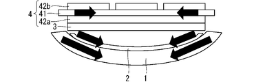
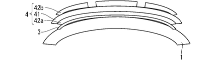
- FIG. 1 is a side view of the warp control structure of the metal base plate according to the embodiment.
- the warp control structure of the metal base plate constitutes a part of the semiconductor module, and includes the metal base plate 1, the dissimilar metal layer 2, and the insulating substrate 4.
- the metal base plate 1 has a square shape in a plan view of about 100 mm ⁇ 100 mm, and has a thickness of 3.5 mmt or more and 4.0 mmt or less. Further, as the material of the metal base plate 1, a high thermal conductive material such as aluminum, an aluminum alloy, or copper is desirable. In this embodiment, aluminum is selected in order to reduce the total weight.
- the dissimilar metal layer 2 is formed only on the entire surface of the metal base plate 1 or only in the region where the insulating substrate 4 is joined on the surface of the metal base plate 1, and has a thickness of about 0.5 mmt.
- the bonding material 3 applied to bond the insulating substrate 4 to the dissimilar metal layer 2 has good wettability, and copper or nickel is preferable. Nickel is selected in this embodiment.
- Examples of the method for forming the dissimilar metal layer 2 include a cold spray method and a metal pasting method.
- the insulating substrate 4 is bonded to the surface of the dissimilar metal layer 2 via a bonding material 3.
- a brazing material, solder, or the like is used as the bonding material 3, but solder is desirable in consideration of manufacturing cost and versatility.
- the thickness of the bonding material 3 which is solder is preferably 0.2 mmt or more and 0.4 mmt or less in consideration of heat dissipation.
- the back surface of the metal base plate 1, which is the surface opposite to the surface on which the dissimilar metal layer 2 is formed, is attached to the cooling fins or the water-cooled jacket via grease. When the metal base plate 1 is attached to the water-cooled jacket, pin fins or straight fins may be formed on the back surface of the metal base plate 1 depending on the refrigerant.
- the insulating substrate 4 has a square shape in a plan view of about 70 mm ⁇ 70 mm, and includes a ceramic substrate 41 and metal plates 42a and 42b.
- a ceramic substrate 41 As the material of the ceramic substrate 41, an appropriate ceramic is selected from ceramics such as alumina, AlN, and Si 3 N 4 according to the application. However, when the warp generated during assembly of the semiconductor module is large (500 ⁇ m or more), it is desirable to select Si 3 N 4 having high bending strength. At that time, the thickness of the ceramic substrate 41 is selected to be 0.32 mmt or 0.64 mmt depending on the withstand voltage with respect to the working voltage.
- the metal plates 42a and 42b are formed on the back surface and the front surface of the ceramic substrate 41, respectively. Further, although aluminum or copper is generally used as the material of the metal plates 42a and 42b, it is desirable that copper is selected in consideration of heat dissipation, and copper is selected in the present embodiment. Further, the thickness of copper is preferably selected in the range of 0.3 mmt or more and 0.8 mmt or less in consideration of heat dissipation and ease of manufacture.
- the materials of the base plate 1, the dissimilar metal layers 2 and the metal plates 42a and 42b are such that the linear expansion coefficient of the metal base plate 1 is ⁇ 1, the linear expansion coefficient of the dissimilar metal layer 2 is ⁇ 2, and the linear expansion coefficients of the metal plates 42a and 42b.
- ⁇ 3 it is selected so as to satisfy ⁇ 1> ⁇ 3> ⁇ 2.
- FIG. 4 is a side view showing a state when the temperature of the metal base plate 1 is changed from room temperature to high temperature in the related technology.
- FIG. 5 is a side view showing a state immediately after the insulating substrate 4 is bonded to the metal base plate 1 in a high temperature state in the related technology.
- FIG. 6 is a side view showing a state when the temperature of the metal base plate 1 and the insulating substrate 4 is changed from high temperature to room temperature in the related technology.
- the dissimilar metal layer 2 is not formed on the surface of the metal base plate 1, and the insulating substrate 4 is bonded to the surface of the metal base plate 1 via the bonding material 3.
- a temperature raising step of raising the temperature of the metal base plate 1 from room temperature to a high temperature is performed. As shown in FIG. 4, the metal base plate 1 does not warp in the temperature raising step and remains flat.
- a joining step of joining the insulating substrate 4 to the surface of the metal base plate 1 via the bonding material 3 is performed in a high temperature state. As shown in FIG. 5, immediately after the joining step, the metal base plate 1 does not warp and remains flat.
- a temperature lowering step is performed in which the temperature of the metal base plate 1 is changed from a high temperature to a room temperature.
- the temperature lowering step as shown by the arrow in FIG. 5, since the linear expansion coefficients of the metal base plate 1 and the insulating substrate 4 are different, the shrinkage amount of the metal base plate 1 and the insulating substrate 4 is different. Therefore, as shown in FIG. 6, in the temperature lowering step after joining, a convex warp occurs on the surface side of the metal base plate 1 to which the insulating substrate 4 is joined.
- the length of the arrow in FIG. 5 indicates the amount of shrinkage between the metal base plate 1 and the insulating substrate 4.
- FIG. 2 is a side view showing a state when the temperature of the metal base plate 1 is changed from room temperature to high temperature in the embodiment.
- FIG. 3 is a side view showing a state immediately after the insulating substrate 4 is bonded to the metal base plate 1 in a high temperature state in the embodiment.
- a temperature raising step of raising the temperature of the metal base plate 1 from room temperature to a high temperature is performed. Since the linear expansion coefficients of the metal base plate 1 and the dissimilar metal layer 2 are different, the expansion amounts of the metal base plate 1 and the dissimilar metal layer 2 are different. As shown in FIG. 2, in the temperature raising step, a convex warp occurs on the side of the metal base plate 1 opposite to the surface to which the insulating substrate 4 is joined.
- the insulating substrate 4 is joined to the surface of the dissimilar metal layer 2 via the bonding material 3 at a high temperature.
- the metal base plate 1 is joined to the insulating substrate 4 in a state of being convexly warped on the side opposite to the surface to which the insulating substrate 4 is bonded. Further, immediately after the joining step, the warp of the metal base plate 1 does not change.
- the metal base plate 1 becomes substantially flat.
- the length of the arrow in FIG. 3 indicates the amount of shrinkage of the metal base plate 1, the dissimilar metal layer 2, and the insulating substrate 4.
- the temperature change from normal temperature (25 ° C.) to high temperature (250 ° C.) and from high temperature (250 ° C.) to normal temperature (25 ° C.) when the dissimilar metal layer 2 is copper or nickel in the present embodiment.
- Table 1 shows the simulation results of warpage due to temperature changes.
- the coefficient of linear expansion of the dissimilar metal layer 2 is the coefficient of linear expansion of the metal plates 42a and 42b as compared with the case where the coefficient of linear expansion of the dissimilar metal layer 2 and the metal plates 42a and 42b are aligned (comparative example). It was found that the warp after joining was reduced when the value was lower than that (in the embodiment).
- the thickness of the metal base plate 1 is 4 mmt
- the thickness of the dissimilar metal layer 2 is 0.5 mmt
- the thicknesses of the metal plates 42a and 42b are 0.4 mmt.
- the semiconductor element is mounted, wired, and case on the bonded body in which the insulating substrate 4 is bonded to the surface of the dissimilar metal layer 2 formed on the metal base plate 1 via the bonding material 3 in a high temperature state.
- the semiconductor module is assembled by attaching and sealing with gel or resin.
- the semiconductor module is cooled by indirect cooling arranged on the cooling fins via grease or the like or direct cooling arranged directly on the water cooling jacket.
- the semiconductor module is incorporated as a component of an inverter device while being arranged on a cooling fin or a water cooling jacket.
- the warp control structure of the metal base plate 1 is joined to the metal base plate 1, the dissimilar metal layer 2 formed on the surface of the metal base plate 1, and the surface of the dissimilar metal layer 2. It is provided with an insulating substrate 4 having metal plates 42a and 42b joined via a material 3 and arranged on both sides, the linear expansion coefficient of the metal base plate 1 is ⁇ 1, and the linear expansion coefficient of the dissimilar metal layer 2 is ⁇ 2.
- the linear expansion coefficient of the metal plates 42a and 42b is ⁇ 3, ⁇ 1> ⁇ 3> ⁇ 2 is satisfied.
- the metal base plate 1 expands with respect to the dissimilar metal layer 2 due to the difference in linear expansion coefficient between the metal base plate 1 and the dissimilar metal layer 2.
- the metal base plate 1 warps convexly on the side opposite to the surface to which the insulating substrate 4 is joined.
- the metal base plates 1 warp in opposite directions, so that the warpage is canceled. This makes it possible to control the warp of the metal base plate 1 that occurs when the temperature changes from high temperature to room temperature.
- the metal base plate 1 is made of aluminum or an aluminum alloy
- the dissimilar metal layer 2 is made of nickel
- the metal plates 42a and 42b are made of copper. Therefore, by adopting an inexpensive aluminum or an aluminum alloy having good thermal conductivity for the metal base plate 1, the heat dissipation of the semiconductor module and the inverter device can be improved. Further, by adopting nickel for the dissimilar metal layer 2, the wettability of the bonding material 3 can be ensured. Further, although aluminum or copper is generally used for the metal plates 42a and 42b, copper is selected from the viewpoint of the coefficient of linear expansion.
- the bonding material 3 is solder, the cost of joining can be reduced by using a highly versatile solder for the bonding material 3. Further, the amount of warpage of the metal base plate 1 that is convexly warped on the side opposite to the surface to which the insulating substrate 4 is bonded due to the temperature change from normal temperature to high temperature, and the temperature change from high temperature to normal temperature after joining the insulating substrate 4
- the amount of warpage convexly on the surface side to which the insulating substrate 4 is joined in the metal base plate 1 does not completely match, and the difference in the amount of warpage increases as the temperature difference between normal temperature and high temperature increases. Therefore, the smaller the temperature difference between normal temperature and high temperature, the more desirable final shape can be obtained in the bonded body.
- the bonding temperature of the solder is 250 ° C. or higher and 300 ° C. or lower, and the temperature difference from the normal temperature is an appropriate temperature, so that a desired final shape can be obtained in the bonded body.
- the semiconductor module includes a warp control structure of a metal base plate and a semiconductor element mounted on the surface of the insulating substrate 4. Therefore, by controlling the warp of the metal base plate 1, the yield of the semiconductor module can be improved.
- the inverter device includes a semiconductor module. Therefore, stable contact between the semiconductor module and the cooling fins or the water-cooled jacket can be performed, so that the yield of the inverter device can be improved.
- 1 metal base plate 1 metal base plate, 2 dissimilar metal layers, 3 bonding materials, 4 insulating substrates, 42a, 42b metal plates.
Landscapes
- Cooling Or The Like Of Semiconductors Or Solid State Devices (AREA)
Abstract
L'objet de la présente invention est de mettre en œuvre une technologie qui contrôle le gauchissement d'une plaque de base en métal généré lorsque la température passe d'une température élevée à la température ambiante, en procédant au gauchissement de la plaque de base en métal dans un changement de température de la température ambiante à la température élevée. Cette structure de contrôle de gauchissement pour une plaque de base en métal (1) comprend une plaque de base en métal (1), une couche de métal dissimilaire (2), et un substrat d'isolation (4). La couche de métal dissimilaire était formée sur la surface de la plaque de base en métal (1). Le substrat d'isolation (4) a des plaques de métal (42a, 42b) soudées à la surface de la couche de métal dissimilaire (2) par le biais d'un matériau de soudage (3) et agencées sur ses deux surfaces. Lorsque le coefficient d'expansion linéaire de la plaque de base en métal (1) est α1, que le coefficient d'expansion linéaire de la couche de métal dissimilaire (2) est α2, et que le coefficient d'expansion linéaire des plaques de métal (42a, 42b) est α3, la relation α1 > α3 > α2 est satisfaite.
Priority Applications (6)
| Application Number | Priority Date | Filing Date | Title |
|---|---|---|---|
| PCT/JP2019/022519 WO2020245975A1 (fr) | 2019-06-06 | 2019-06-06 | Structure de contrôle de gauchissement pour plaque de base en métal, module semi-conducteur, et dispositif d'onduleur |
| CN201980097064.9A CN113906553A (zh) | 2019-06-06 | 2019-06-06 | 金属基座板的翘曲控制构造、半导体模块及逆变器装置 |
| DE112019007396.6T DE112019007396T5 (de) | 2019-06-06 | 2019-06-06 | Struktur zur Steuerung einer Wölbung für eine Metallbasisplatte, Halbleitermodul und Inverter-Vorrichtung |
| US17/439,731 US20220157763A1 (en) | 2019-06-06 | 2019-06-06 | Warpage control structure for metal base plate, semiconductor module, and inverter device |
| JP2021524595A JP7154410B2 (ja) | 2019-06-06 | 2019-06-06 | 金属ベース板の反り制御構造、半導体モジュールおよびインバータ装置 |
| US18/806,198 US20240404979A1 (en) | 2019-06-06 | 2024-08-15 | Warpage control structure for metal base plate, semiconductor module, and inverter device |
Applications Claiming Priority (1)
| Application Number | Priority Date | Filing Date | Title |
|---|---|---|---|
| PCT/JP2019/022519 WO2020245975A1 (fr) | 2019-06-06 | 2019-06-06 | Structure de contrôle de gauchissement pour plaque de base en métal, module semi-conducteur, et dispositif d'onduleur |
Related Child Applications (2)
| Application Number | Title | Priority Date | Filing Date |
|---|---|---|---|
| US17/439,731 A-371-Of-International US20220157763A1 (en) | 2019-06-06 | 2019-06-06 | Warpage control structure for metal base plate, semiconductor module, and inverter device |
| US18/806,198 Continuation US20240404979A1 (en) | 2019-06-06 | 2024-08-15 | Warpage control structure for metal base plate, semiconductor module, and inverter device |
Publications (1)
| Publication Number | Publication Date |
|---|---|
| WO2020245975A1 true WO2020245975A1 (fr) | 2020-12-10 |
Family
ID=73653113
Family Applications (1)
| Application Number | Title | Priority Date | Filing Date |
|---|---|---|---|
| PCT/JP2019/022519 Ceased WO2020245975A1 (fr) | 2019-06-06 | 2019-06-06 | Structure de contrôle de gauchissement pour plaque de base en métal, module semi-conducteur, et dispositif d'onduleur |
Country Status (5)
| Country | Link |
|---|---|
| US (2) | US20220157763A1 (fr) |
| JP (1) | JP7154410B2 (fr) |
| CN (1) | CN113906553A (fr) |
| DE (1) | DE112019007396T5 (fr) |
| WO (1) | WO2020245975A1 (fr) |
Families Citing this family (2)
| Publication number | Priority date | Publication date | Assignee | Title |
|---|---|---|---|---|
| CN114959701A (zh) * | 2022-05-13 | 2022-08-30 | 济南晶正电子科技有限公司 | 一种复合薄膜、制备方法及电子元器件 |
| CN117794155A (zh) * | 2022-09-21 | 2024-03-29 | 技嘉科技股份有限公司 | 散热装置 |
Citations (5)
| Publication number | Priority date | Publication date | Assignee | Title |
|---|---|---|---|---|
| JPH1117081A (ja) * | 1997-06-19 | 1999-01-22 | Sansha Electric Mfg Co Ltd | 電力用半導体モジュール |
| JP2002237556A (ja) * | 2001-02-09 | 2002-08-23 | Mitsubishi Electric Corp | パワー半導体装置 |
| JP2002270748A (ja) * | 2001-03-09 | 2002-09-20 | Hitachi Ltd | 半導体モジュール及び電力変換装置 |
| JP2004207619A (ja) * | 2002-12-26 | 2004-07-22 | Mitsubishi Materials Corp | パワーモジュール用基板及びパワーモジュール |
| JP2008147308A (ja) * | 2006-12-07 | 2008-06-26 | Hitachi Metals Ltd | 回路基板およびこれを用いた半導体モジュール |
Family Cites Families (13)
| Publication number | Priority date | Publication date | Assignee | Title |
|---|---|---|---|---|
| JP2003046032A (ja) | 2001-07-26 | 2003-02-14 | Hitachi Ltd | 銅複合材放熱基板、半導体パワーモジュール及びその製造方法 |
| KR101030068B1 (ko) * | 2002-07-08 | 2011-04-19 | 니치아 카가쿠 고교 가부시키가이샤 | 질화물 반도체 소자의 제조방법 및 질화물 반도체 소자 |
| JP5028147B2 (ja) * | 2007-05-29 | 2012-09-19 | 株式会社アライドマテリアル | 半導体装置用ヒートスプレッダとその製造方法 |
| KR101093719B1 (ko) * | 2010-01-04 | 2011-12-19 | (주)웨이브닉스이에스피 | 금속기판을 이용한 고출력 소자의 패키지 모듈 구조 및 그 제조방법 |
| US8519532B2 (en) | 2011-09-12 | 2013-08-27 | Infineon Technologies Ag | Semiconductor device including cladded base plate |
| JP5588956B2 (ja) * | 2011-11-30 | 2014-09-10 | 株式会社 日立パワーデバイス | パワー半導体装置 |
| JP2014112732A (ja) * | 2012-03-30 | 2014-06-19 | Mitsubishi Materials Corp | ヒートシンク付パワーモジュール用基板及びパワーモジュール |
| CN205752150U (zh) * | 2013-08-28 | 2016-11-30 | 三菱电机株式会社 | 半导体装置 |
| CN204045563U (zh) * | 2014-01-25 | 2014-12-24 | 嘉兴斯达半导体股份有限公司 | 功率半导体用新型金属-陶瓷绝缘基板 |
| EP3321957B1 (fr) * | 2015-07-09 | 2022-07-27 | Kabushiki Kaisha Toshiba | Carte de circuit imprimé céramique-métal et dispositif à semi-conducteur l'utilisant |
| JP6451866B2 (ja) * | 2015-11-16 | 2019-01-16 | 株式会社豊田中央研究所 | 接合構造体およびその製造方法 |
| JP7031172B2 (ja) * | 2017-08-24 | 2022-03-08 | 富士電機株式会社 | 半導体装置 |
| JP7183551B2 (ja) * | 2018-03-15 | 2022-12-06 | 富士電機株式会社 | 半導体装置 |
-
2019
- 2019-06-06 WO PCT/JP2019/022519 patent/WO2020245975A1/fr not_active Ceased
- 2019-06-06 US US17/439,731 patent/US20220157763A1/en not_active Abandoned
- 2019-06-06 JP JP2021524595A patent/JP7154410B2/ja active Active
- 2019-06-06 DE DE112019007396.6T patent/DE112019007396T5/de active Pending
- 2019-06-06 CN CN201980097064.9A patent/CN113906553A/zh active Pending
-
2024
- 2024-08-15 US US18/806,198 patent/US20240404979A1/en active Pending
Patent Citations (5)
| Publication number | Priority date | Publication date | Assignee | Title |
|---|---|---|---|---|
| JPH1117081A (ja) * | 1997-06-19 | 1999-01-22 | Sansha Electric Mfg Co Ltd | 電力用半導体モジュール |
| JP2002237556A (ja) * | 2001-02-09 | 2002-08-23 | Mitsubishi Electric Corp | パワー半導体装置 |
| JP2002270748A (ja) * | 2001-03-09 | 2002-09-20 | Hitachi Ltd | 半導体モジュール及び電力変換装置 |
| JP2004207619A (ja) * | 2002-12-26 | 2004-07-22 | Mitsubishi Materials Corp | パワーモジュール用基板及びパワーモジュール |
| JP2008147308A (ja) * | 2006-12-07 | 2008-06-26 | Hitachi Metals Ltd | 回路基板およびこれを用いた半導体モジュール |
Also Published As
| Publication number | Publication date |
|---|---|
| JP7154410B2 (ja) | 2022-10-17 |
| JPWO2020245975A1 (ja) | 2021-10-21 |
| US20220157763A1 (en) | 2022-05-19 |
| CN113906553A (zh) | 2022-01-07 |
| DE112019007396T5 (de) | 2022-02-17 |
| US20240404979A1 (en) | 2024-12-05 |
Similar Documents
| Publication | Publication Date | Title |
|---|---|---|
| KR102232098B1 (ko) | 히트 싱크가 부착된 파워 모듈용 기판 및 그 제조 방법 | |
| TWI690041B (zh) | 具有散熱片的電源模組用基板及電源模組 | |
| CN102208378B (zh) | 冷却装置 | |
| US9786577B2 (en) | Power module substrate, heat-sink-attached power-module substrate, and heat-sink-attached power module | |
| TW201626513A (zh) | 功率模組用基板單元及功率模組 | |
| WO2013141110A1 (fr) | Procédé de fabrication de substrat à radiateur intégré, et substrat à radiateur intégré | |
| JP6201827B2 (ja) | 放熱板付パワーモジュール用基板の製造方法 | |
| TW201611208A (zh) | 功率模組用基板單元及功率模組 | |
| JP7159395B2 (ja) | 回路基板および半導体モジュール | |
| US20240404979A1 (en) | Warpage control structure for metal base plate, semiconductor module, and inverter device | |
| CN106463477A (zh) | 功率模块用基板单元及功率模块 | |
| JP2012160548A (ja) | 絶縁基板とその絶縁基板を有するパワーモジュール | |
| JP6201828B2 (ja) | 放熱板付パワーモジュール用基板の製造方法 | |
| JP6011552B2 (ja) | ヒートシンク付パワーモジュール用基板及びその製造方法 | |
| JP2010199251A (ja) | 半導体装置の製造方法 | |
| JP6264822B2 (ja) | ヒートシンク付パワーモジュール用基板及びその製造方法 | |
| WO2019167942A1 (fr) | Carte de circuit imprimé isolante | |
| JP7054073B2 (ja) | ヒートシンク付き絶縁回路基板 | |
| JP2012009787A (ja) | パワーモジュール用基板及びその製造方法 | |
| JP2017011293A (ja) | ヒートシンク付パワーモジュール用基板及びその製造方法 | |
| JP2000332170A (ja) | 半導体装置 | |
| JP2013211288A (ja) | ヒートシンク付パワーモジュール用基板の製造方法 | |
| JP7467936B2 (ja) | ヒートシンク付絶縁回路基板、電子部品及びヒートシンク付絶縁回路基板の製造方法 | |
| JP6264889B2 (ja) | ヒートシンク付パワーモジュール用基板及びその製造方法 | |
| JP2002252433A (ja) | セラミックス回路基板及びその製造方法 |
Legal Events
| Date | Code | Title | Description |
|---|---|---|---|
| 121 | Ep: the epo has been informed by wipo that ep was designated in this application |
Ref document number: 19931627 Country of ref document: EP Kind code of ref document: A1 |
|
| ENP | Entry into the national phase |
Ref document number: 2021524595 Country of ref document: JP Kind code of ref document: A |
|
| 122 | Ep: pct application non-entry in european phase |
Ref document number: 19931627 Country of ref document: EP Kind code of ref document: A1 |