WO2020262013A1 - Unité de filtre - Google Patents
Unité de filtre Download PDFInfo
- Publication number
- WO2020262013A1 WO2020262013A1 PCT/JP2020/022982 JP2020022982W WO2020262013A1 WO 2020262013 A1 WO2020262013 A1 WO 2020262013A1 JP 2020022982 W JP2020022982 W JP 2020022982W WO 2020262013 A1 WO2020262013 A1 WO 2020262013A1
- Authority
- WO
- WIPO (PCT)
- Prior art keywords
- core
- filter unit
- capacitor
- wiring
- facing
- Prior art date
- Legal status (The legal status is an assumption and is not a legal conclusion. Google has not performed a legal analysis and makes no representation as to the accuracy of the status listed.)
- Ceased
Links
Images


Classifications
-
- H—ELECTRICITY
- H01—ELECTRIC ELEMENTS
- H01F—MAGNETS; INDUCTANCES; TRANSFORMERS; SELECTION OF MATERIALS FOR THEIR MAGNETIC PROPERTIES
- H01F17/00—Fixed inductances of the signal type
- H01F17/04—Fixed inductances of the signal type with magnetic core
-
- H—ELECTRICITY
- H03—ELECTRONIC CIRCUITRY
- H03H—IMPEDANCE NETWORKS, e.g. RESONANT CIRCUITS; RESONATORS
- H03H7/00—Multiple-port networks comprising only passive electrical elements as network components
- H03H7/01—Frequency selective two-port networks
- H03H7/0115—Frequency selective two-port networks comprising only inductors and capacitors
-
- H—ELECTRICITY
- H01—ELECTRIC ELEMENTS
- H01F—MAGNETS; INDUCTANCES; TRANSFORMERS; SELECTION OF MATERIALS FOR THEIR MAGNETIC PROPERTIES
- H01F27/00—Details of transformers or inductances, in general
-
- H—ELECTRICITY
- H01—ELECTRIC ELEMENTS
- H01F—MAGNETS; INDUCTANCES; TRANSFORMERS; SELECTION OF MATERIALS FOR THEIR MAGNETIC PROPERTIES
- H01F27/00—Details of transformers or inductances, in general
- H01F27/24—Magnetic cores
-
- H—ELECTRICITY
- H01—ELECTRIC ELEMENTS
- H01F—MAGNETS; INDUCTANCES; TRANSFORMERS; SELECTION OF MATERIALS FOR THEIR MAGNETIC PROPERTIES
- H01F27/00—Details of transformers or inductances, in general
- H01F27/28—Coils; Windings; Conductive connections
- H01F27/2823—Wires
-
- H—ELECTRICITY
- H01—ELECTRIC ELEMENTS
- H01F—MAGNETS; INDUCTANCES; TRANSFORMERS; SELECTION OF MATERIALS FOR THEIR MAGNETIC PROPERTIES
- H01F27/00—Details of transformers or inductances, in general
- H01F27/28—Coils; Windings; Conductive connections
- H01F27/2847—Sheets; Strips
-
- H—ELECTRICITY
- H01—ELECTRIC ELEMENTS
- H01F—MAGNETS; INDUCTANCES; TRANSFORMERS; SELECTION OF MATERIALS FOR THEIR MAGNETIC PROPERTIES
- H01F27/00—Details of transformers or inductances, in general
- H01F27/40—Structural association with built-in electric component, e.g. fuse
-
- H—ELECTRICITY
- H03—ELECTRONIC CIRCUITRY
- H03H—IMPEDANCE NETWORKS, e.g. RESONANT CIRCUITS; RESONATORS
- H03H1/00—Constructional details of impedance networks whose electrical mode of operation is not specified or applicable to more than one type of network
- H03H1/0007—Constructional details of impedance networks whose electrical mode of operation is not specified or applicable to more than one type of network of radio frequency interference filters
-
- H—ELECTRICITY
- H03—ELECTRONIC CIRCUITRY
- H03H—IMPEDANCE NETWORKS, e.g. RESONANT CIRCUITS; RESONATORS
- H03H7/00—Multiple-port networks comprising only passive electrical elements as network components
- H03H7/01—Frequency selective two-port networks
- H03H7/09—Filters comprising mutual inductance
-
- H—ELECTRICITY
- H01—ELECTRIC ELEMENTS
- H01G—CAPACITORS; CAPACITORS, RECTIFIERS, DETECTORS, SWITCHING DEVICES, LIGHT-SENSITIVE OR TEMPERATURE-SENSITIVE DEVICES OF THE ELECTROLYTIC TYPE
- H01G4/00—Fixed capacitors; Processes of their manufacture
- H01G4/38—Multiple capacitors, i.e. structural combinations of fixed capacitors
- H01G4/385—Single unit multiple capacitors, e.g. dual capacitor in one coil
-
- H—ELECTRICITY
- H01—ELECTRIC ELEMENTS
- H01G—CAPACITORS; CAPACITORS, RECTIFIERS, DETECTORS, SWITCHING DEVICES, LIGHT-SENSITIVE OR TEMPERATURE-SENSITIVE DEVICES OF THE ELECTROLYTIC TYPE
- H01G4/00—Fixed capacitors; Processes of their manufacture
- H01G4/40—Structural combinations of fixed capacitors with other electric elements, the structure mainly consisting of a capacitor, e.g. RC combinations
-
- H—ELECTRICITY
- H03—ELECTRONIC CIRCUITRY
- H03H—IMPEDANCE NETWORKS, e.g. RESONANT CIRCUITS; RESONATORS
- H03H1/00—Constructional details of impedance networks whose electrical mode of operation is not specified or applicable to more than one type of network
- H03H2001/0021—Constructional details
Definitions
- the present invention relates to a filter unit.
- the filter described in Patent Document 1 includes an inductor and a capacitor.
- the inductor comprises a wiring and a core surrounding the wiring.
- the capacitor When downsizing the filter, the capacitor is placed near the core. When current flows through the wiring, a noise-based magnetic field is created in the core. When a capacitor is affected by a magnetic field, the damping characteristics of the filter can deteriorate.
- An object of the present invention is to provide a filter unit capable of suppressing a decrease in attenuation characteristics with respect to noise.
- a capacitor, an inductor having a wiring and a core are provided, and the core includes an annular core body through which the wiring is passed and the core.
- a filter unit is provided that includes a facing portion extending from the main body to a position facing the capacitor.
- FIG. 2 is a sectional view taken along line 3-3 of FIG. The cross-sectional view which shows by breaking a part of the filter unit.
- FIG. 2 is a sectional view taken along line 6-6 of FIG.
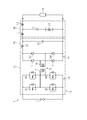
- the vehicle 10 includes a battery 11 and a power conversion device 12.
- the power conversion device 12 includes a DC / DC converter 13, a filter 20, and a filter unit 30.
- the vehicle 10 is an electric vehicle whose drive source is an electric motor or a hybrid vehicle.
- the battery 11 is used as a power source for an electric motor mounted on the vehicle 10.
- a chargeable / discharging power storage device such as a lithium ion secondary battery or a nickel hydrogen storage battery is used.
- the power converter 12 is electrically connected to the load 19 in the home.
- the power conversion device 12 supplies electric power to the load 19 in the home.
- the DC / DC converter 13 includes a bridge circuit 14, a transformer 15, and a rectifier circuit 16.
- the bridge circuit 14 is provided on the primary side of the transformer 15 and includes four switching elements Q1 to Q4.
- the switching elements Q1 and Q2 are connected in series with each other.
- the switching elements Q3 and Q4 are connected in series with each other.
- the rectifier circuit 16 is provided on the secondary side of the transformer 15 and includes four diodes D1 to D4.
- the diodes D1 and D2 are connected in series with each other.
- the diodes D3 and D4 are connected in series with each other.
- the transformer 15 includes a primary winding 17 and a secondary winding 18.
- the primary winding 17 is connected to a connection point between the switching elements Q1 and Q2 and a connection point between the switching elements Q3 and Q4.
- the secondary winding 18 is connected to a connection point between the diodes D1 and D2 and a connection point between the diodes D3 and D4.
- the DC power input from the battery 11 is stepped down by the switching operation of the switching elements Q1 to Q4.
- the switching frequencies of the switching elements Q1 to Q4 are 150 kHz to 200 kHz.
- the DC / DC converter 13 outputs the stepped-down DC power to the filter 20.
- the full-bridge type DC / DC converter 13 is used, but any type of DC / DC converter such as the half-bridge type may be used.
- the filter 20 includes a smoothing coil 21 and a smoothing capacitor 22.
- the filter 20 is an LC filter composed of a smoothing coil 21 and a smoothing capacitor 22.
- the filter 20 attenuates noise in a desired frequency band.
- the smoothing coil 21 smoothes the output power including the ripple rectified by the rectifier circuit 16.
- the filter unit 30 includes a substrate 31, a capacitor C mounted on the substrate 31, and two inductors L1 and L2. Although not shown, the DC / DC converter 13 and the filter 20 are also mounted on the substrate 31.
- the inductors L1 and L2 include a wiring 36 serving as a power line and a core 50.
- the substrate 31 includes an insulating layer 32, a pattern 35 to which the capacitor C is connected, and a via 37 to connect the pattern 35 and the wiring 36.
- One of both sides of the insulating layer 32 in the thickness direction is the first surface 33, and the other is the second surface 34.
- the pattern 35 is provided on the first surface 33.
- the wiring 36 is provided on the second surface 34.
- the pattern 35 intersects the wiring 36 when viewed from the thickness direction of the substrate 31.
- As the pattern 35 for example, a copper foil is used.
- a bus bar is used as the wiring 36.
- the capacitor C is connected to the pattern 35 by a bonding material such as solder.
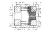
- the insulating layer 32 includes four holes 41 to 44 penetrating in the thickness direction of the substrate 31.
- the position where the pattern 35 and the wiring 36 intersect on the substrate 31 is defined as the intersection X.
- the periphery of the intersection X is divided into four regions A1, A2, A3, and A4 by the pattern 35 and the wiring 36.
- One hole 41 to 44 is provided in each of the four regions A1 to A4.
- the four holes 41 to 44 are arranged on both sides of the pattern 35 and on both sides of the wiring 36, respectively.
- the first hole 41 is one of the four holes 41 to 44.
- the second hole 42 is provided so as to arrange the wiring 36 between the second hole 42 and the first hole 41.
- the third hole 43 is provided so as to arrange the pattern 35 between the third hole 43 and the first hole 41.
- the fourth hole 44 is provided so as to arrange the wiring 36 between the fourth hole 44 and the third hole 43.
- the separation distance between the central axis of the first hole 41 and the central axis of the second hole 42 is the same as the separation distance between the central axis of the third hole 43 and the central axis of the fourth hole 44.
- the separation distance between the central axis of the first hole 41 and the central axis of the third hole 43 is the same as the separation distance between the central axis of the second hole 42 and the central axis of the fourth hole 44.
- Capacitor C is arranged in two places.
- the capacitor C is arranged between the first hole 41 and the third hole 43, and between the second hole 42 and the fourth hole 44.
- a plurality of capacitors C are provided on the pattern 35.
- FIG. 1 shows the combined capacitance of a plurality of capacitors C as one capacitor C.
- the core 50 is divided into two parts.
- a dust core produced by high-pressure press molding of a metallic magnetic powder together with a binder is used.
- any core such as a ferrite core may be used.
- the core 50 includes a first core 51 and a second core 71.
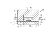
- the first core 51 includes a rectangular plate-shaped pedestal 52 and legs 53 to 56 provided at each of the four corners of the pedestal 52.
- the legs 53 to 56 are columnar.
- the legs 53 to 56 project in the thickness direction of the pedestal 52.
- the legs 53 to 56 project from the pedestal 52 in the same direction.
- the first leg 53 is one of the four legs 53-56.
- the second leg portion 54 is arranged adjacent to the first leg portion 53 in the lateral direction of the pedestal 52.
- the third leg portion 55 is arranged adjacent to the first leg portion 53 in the longitudinal direction of the pedestal 52.
- the fourth leg portion 56 is arranged adjacent to the third leg portion 55 in the lateral direction of the pedestal 52.
- the separation distance between the central axis of the first leg portion 53 and the central axis of the second leg portion 54 is the same as the separation distance between the central axis of the first hole 41 and the central axis of the second hole 42.
- the separation distance between the central axis of the first leg portion 53 and the central axis of the third leg portion 55 is the same as the separation distance between the central axis of the first hole 41 and the central axis of the third hole 43.
- the portion connecting the first leg portion 53 and the second leg portion 54 is referred to as the first connecting portion 61
- the portion connecting the third leg portion 55 and the fourth leg portion 56 is referred to as the second connecting portion 62.
- the first connecting portion 61 includes a portion of the pedestal 52 facing the first leg portion 53, a portion facing the second leg portion 54, and a portion between the first leg portion 53 and the second leg portion 54.
- the second connecting portion 62 includes a portion of the pedestal 52 facing the third leg portion 55, a portion facing the fourth leg portion 56, and a portion between the third leg portion 55 and the fourth leg portion 56.
- the portion connecting the first leg portion 53 and the third leg portion 55 is referred to as the third connecting portion 63
- the portion connecting the second leg portion 54 and the fourth leg portion 56 is referred to as the fourth connecting portion 64.
- the third connecting portion 63 includes a portion of the pedestal 52 facing the first leg portion 53, a portion facing the third leg portion 55, and a portion between the first leg portion 53 and the third leg portion 55.
- the fourth connecting portion 64 includes a portion of the pedestal 52 facing the second leg portion 54, a portion facing the fourth leg portion 56, and a portion between the second leg portion 54 and the fourth leg portion 56.
- the third connecting portion 63 shares a portion of the pedestal 52 facing the first leg portion 53 with the first connecting portion 61.
- the third connecting portion 63 shares a portion of the pedestal 52 facing the third leg portion 55 with the second connecting portion 62.
- the fourth connecting portion 64 shares a portion of the pedestal 52 facing the second leg portion 54 with the first connecting portion 61.
- the fourth connecting portion 64 shares a portion of the pedestal 52 facing the fourth leg portion 56 with the second connecting portion 62.
- the facing portion 65 connects the first connecting portion 61 and the second connecting portion 62.
- a part of the facing portion 65 is a part of the third connecting portion 63 and the fourth connecting portion 64.
- the second core 71 has a square plate shape.
- the second core 71 may have a size that allows all four legs 53 to 56 to come into contact with each other when the second core 71 is overlapped with the first core 51.
- the thickness direction surface of the second core 71 has the same shape as the thickness direction surface of the pedestal 52.
- the first core 51 and the second core 71 are arranged so that the substrate 31 is located between the pedestal 52 and the second core 71.
- the first core 51 is arranged so that the pedestal 52 faces the first surface 33 of the substrate 31.
- the second core 71 is arranged so as to face the second surface 34 of the substrate 31.
- the legs 53 to 56 of the first core 51 are inserted into the holes 41 to 44.
- the first leg 53 is inserted into the first hole 41
- the second leg 54 is inserted into the second hole 42
- the third leg 55 is inserted into the third hole 43
- the fourth leg 56 is inserted into the fourth hole 44.
- Each leg portion 53 to 56 penetrates the insulating layer 32.
- the legs 53 to 56 are in contact with the second core 71.
- the legs 53 to 56 of the first core 51 are in contact with the four corners of the second core 71.
- the second core 71 faces the entire first core 51 while arranging the substrate 31 between the second core 71 and the first core 51.
- the core 50 is composed of the pedestal 52, the legs 53 to 56, and the second core 71. It includes two core bodies 81 and 82.
- One core body 81 is composed of the first leg portion 53, the second leg portion 54, the first connecting portion 61, and the first portion 72 of the second core 71.
- the first portion 72 is a portion of the second core 71 facing the first connecting portion 61 via the substrate 31, the first leg portion 53, and the second leg portion 54.
- One core body 82 is composed of the third leg portion 55, the fourth leg portion 56, the second connecting portion 62, and the second portion 73 of the second core 71.
- the second portion 73 is a portion of the second core 71 facing the second connecting portion 62 via the substrate 31, the third leg portion 55, and the fourth leg portion 56.
- the facing portion 65 connects the core main bodies 81 and 82.
- the second core 71 has a third site 74 between the first site 72 and the second site 73.
- the third portion 74 also connects the core bodies 81 and 82.
- the core bodies 81 and 82 have the same shape.
- the core bodies 81 and 82 are annular and include a wiring hole 83.
- the wiring 36 is passed through the wiring hole 83.
- the core bodies 81 and 82 are arranged so that their central axes face the same direction. The same direction here allows a slight error within the tolerance.
- the wiring 36 passes through the wiring holes 83 of the core bodies 81 and 82 in a straight line.
- the core 50 acts on a magnetic field generated by a current flowing through the wiring 36 to form inductors L1 and L2.
- the inductors L1 and L2 are formed by the wiring 36 and the core bodies 81 and 82, respectively, but it can be considered that one inductor is formed by the wiring 36 and the core 50.
- Each capacitor C is located between the core bodies 81 and 82.
- the capacitor C is located between the first leg 53 and the third leg 55, and between the second leg 54 and the fourth leg 56.
- the facing portion 65 faces the capacitor C in the thickness direction of the substrate 31. It can be said that the thickness direction of the substrate 31 is the direction in which the insulating layer 32 and the pattern 35 overlap.
- the facing portion 65 extends from each of the core main bodies 81 and 82 to a position facing the capacitor C.
- the facing portion 65 faces all of the plurality of capacitors C.
- the capacitor C is sandwiched between the facing portion 65 and the substrate 31 from the thickness direction of the substrate 31.
- the third portion 74 of the second core 71 extends from each of the core main bodies 81 and 82 to a position facing the capacitor C via the substrate 31.
- the third portion 74 of the second core 71 faces all of the plurality of capacitors C via the substrate 31. It can be said that the capacitor C is sandwiched between the facing portion 65 and the third portion 74 from the thickness direction of the substrate 31.
- the core 50 includes two annular portions 91 and 92 composed of a pedestal 52, legs 53 to 56, and a second core 71.
- One annular portion 91 is formed by the first leg portion 53, the third leg portion 55, the third connecting portion 63, and the second core 71.
- the second leg portion 54, the fourth leg portion 56, the fourth connecting portion 64, and the second core 71 constitute one annular portion 92.
- the annular portions 91 and 92 are provided with connection holes 93.
- the connection hole 93 is a hole through which the pattern 35 is passed.
- the annular portions 91 and 92 are arranged so that their central axes face the same direction. The same direction here allows a slight error within the tolerance.
- the direction along the central axis of the annular portions 91 and 92 and the direction along the central axis of the core bodies 81 and 82 are orthogonal to each other.
- the core 50 includes a wiring hole 83 through which the wiring 36 for forming the inductors L1 and L2 passes, and a connection hole 93 through which the pattern 35 for connecting the capacitor C passes.
- the wiring hole 83 has dimensions in the length direction orthogonal to the central axis of the wiring hole 83 and the thickness direction of the substrate 31.
- the connection hole 93 has dimensions in the length direction orthogonal to the central axis of the connection hole 93 and the thickness direction of the substrate 31.
- the length of the wiring hole 83 is smaller than the length of the connection hole 93.
- the filter unit 30 attenuates the noise contained in the DC power output from the filter 20 and outputs the noise.
- the filter unit 30 of the present embodiment attenuates noise in a frequency band of 150 kHz to 200 kHz or less, which is the switching frequency of the switching elements Q1 to Q4, and a frequency band of 500 kHz or more, which is a frequency used for AM broadcasting.
- the electric power output from the filter unit 30 is supplied to the load 19 in the home.
- the inductors L1 and L2 are configured by the wiring 36 and the annular core bodies 81 and 82 surrounding the wiring 36.
- the impedance of the inductors L1 and L2 becomes higher as the frequency becomes higher. Therefore, high frequency noise is cut.
- a magnetic field corresponding to the noise current is generated in the core 50.
- the noise current is converted into a magnetic field and consumed as a magnetic loss. This reduces the noise current.
- the filter unit 30 includes an inductance component L3 due to the capacitor C and the pattern 35.
- the inductors L1 and L2 and the inductance component L3 are magnetically coupled due to the influence of the magnetic field, a voltage is induced. Due to the influence of this voltage, the attenuation characteristic of the filter unit 30 may deteriorate.
- the filter unit 30 of the present embodiment suppresses the magnetic field coupling between the inductors L1 and L2 and the inductance component L3 by suppressing the influence of the magnetic field on the capacitor C.
- the filter unit of the comparative example has the same configuration as the filter unit of the present embodiment except that the shape of the core is different.
- the filter unit 100 of the comparative example includes a core 101.
- the core 101 includes annular core bodies 102 and 103.
- the core 101 is not provided at a position facing the capacitor C in the thickness direction of the substrate 31. That is, in the core 101 used for the filter unit 100 of the comparative example, the facing portion 65 is omitted from the core 50 of the present embodiment.
- FIG. 8 shows the magnetic field distribution generated inside the core 101 of the filter unit 100 of the comparative example when a current flows through the wiring 36.
- the magnetic field distribution indicates the strength of the magnetic field, that is, the magnetic flux density.
- the strength of the magnetic field is represented by dots, and it can be said that the denser the dots, the stronger the strength of the magnetic field.
- the capacitor C is located at a portion where the magnetic field strength is strong, and the inductors L1 and L2 and the inductance component L3 are likely to be magnetically coupled.
- FIG. 9 shows the magnetic field distribution generated inside the core 50 of the filter unit 30 of the present embodiment when a current flows through the wiring 36.
- the facing portion 65 so as to face the capacitor C, the magnetic field at the position where the capacitor C is provided is weakened as compared with the case where the facing portion 65 is not provided. Can be induced.
- the horizontal axis is frequency
- the attenuation characteristics of the filter units 30 and 100 are shown.
- the attenuation characteristics of the filter unit 100 of the comparative example are shown by a alternate long and short dash line
- the attenuation characteristics of the filter unit 30 of the present embodiment are shown by a solid line.
- the attenuation characteristic is lowered at the boundary of 150 kHz to 200 kHz.
- the filter unit 30 of the present embodiment the deterioration of the attenuation characteristic is suppressed even in the band of 150 kHz to 200 kHz or less. In this way, by inducing the magnetic field by the facing portion 65 so that the strength of the magnetic field at the position where the capacitor C is provided is weakened, it is possible to suppress the deterioration of the attenuation characteristics.
- a frequency band for attenuating the noise is set so that the noise contained in the output power from the DC / DC converter 13 does not flow into the home. It may be required to be wide.
- the filter unit 30 of the present embodiment is required to attenuate noise in a frequency band below the switching frequency and a frequency band above the frequency used for AM broadcasting. It is also conceivable to increase the number of filters and the number of capacitors C in order to attenuate noise over a wide frequency band. However, if the number of filters and capacitors C is increased, the size of the power conversion device 12 is increased.
- the attenuation characteristic against noise is improved by changing the magnetic field distribution. Therefore, as compared with the case where the number of filters and the number of capacitors C are increased, the attenuation characteristics of the filter unit 30 are improved while suppressing the increase in size of the power conversion device 12.
- the core 50 includes an opposing portion 65 facing the capacitor C.
- the strength of the magnetic field at the position where the capacitor C is provided can be weakened as compared with the case where the facing portion 65 is not provided.
- By suppressing the influence of the magnetic field on the capacitor C it is possible to suppress the deterioration of the attenuation characteristic of the filter unit 30.
- the pattern 35 intersects the wiring 36 when viewed from the thickness direction of the substrate 31. Since the wiring 36 and the pattern 35 can be arranged so as to be overlapped with each other when viewed from the thickness direction of the substrate 31, the filter unit 30 can be miniaturized.
- the facing portion 65 connects the core main bodies 81 and 82 to each other. By connecting the core bodies 81 and 82 to each other by the facing portion 65, it is easy to induce the magnetic field so that the magnetic field at the position where the capacitor C is provided is weakened.
- the filter unit 30 is an output filter provided on the secondary side of the transformer 15. Since the step-down is performed by the DC / DC converter 13, the current flowing through the secondary side of the transformer 15 is larger than the current flowing through the primary side of the transformer 15. When the current is large, it is difficult to attenuate the noise. By suppressing the deterioration of the attenuation characteristic of the filter unit 30 as in the embodiment, noise can be efficiently attenuated even when the current is large.
- the facing portion 65 does not have to connect the core main bodies 81 and 82 to each other. In this case, the facing portion 65 is provided on one of the core main bodies 81 and 82.
- the core 50 may include any of the core main bodies 81 and 82.
- the capacitor C may be arranged at any position as long as it is around the core bodies 81 and 82.
- the shape of the facing portion 65 may be changed.
- the facing portion 65 may at least face the capacitor C, and a portion that does not face the facing portion 65 may be omitted.
- the shape of the second core 71 may be changed according to the shape of the facing portion 65. It is preferable that the second core 71 is provided at a position facing the facing portion 65 while arranging the substrate 31 between the first core 51 and the second core 71.
- the pattern 35 does not have to intersect the wiring 36 when viewed from the thickness direction of the substrate 31.
- the facing portion 65 may face the capacitor C in a direction orthogonal to both the thickness direction of the substrate 31 and the central axes of the core bodies 81 and 82. That is, the facing portion 65 may extend from the core bodies 81 and 82 to a position facing the capacitor C, and may face the capacitor C in any direction.
- the facing portion 65 may face at least a part of the plurality of capacitors C.
- the core 50 does not have to be divided into a first core 51 and a second core 71.
- the wiring 36 may be wound around the core bodies 81 and 82.
- the filter unit 30 may be used to attenuate noise contained in AC power.
- the filter unit 30 may be provided in any device as long as it is a device that needs to attenuate noise.
Landscapes
- Engineering & Computer Science (AREA)
- Power Engineering (AREA)
- Microelectronics & Electronic Packaging (AREA)
- Manufacturing & Machinery (AREA)
- Filters And Equalizers (AREA)
- Coils Or Transformers For Communication (AREA)
- Fixed Capacitors And Capacitor Manufacturing Machines (AREA)
Abstract
Une unité de filtre selon la présente invention comprend un substrat, des condensateurs montés sur le substrat, et deux bobines d'induction. Les bobines d'induction comprennent chacune un fil et un noyau. Le noyau comprend deux corps de noyau. Les corps de noyau ont chacun une forme d'anneau et comprennent un trou de câblage. Les condensateurs sont disposés entre les deux corps de noyau. Une section opposée s'étend depuis les deux corps centraux respectifs jusqu'à une position opposée aux condensateurs C. La section opposée est opposée à l'ensemble de la pluralité de condensateurs.
Priority Applications (3)
| Application Number | Priority Date | Filing Date | Title |
|---|---|---|---|
| DE112020003040.7T DE112020003040T5 (de) | 2019-06-27 | 2020-06-11 | Filtereinheit |
| CN202080045842.2A CN114008916B (zh) | 2019-06-27 | 2020-06-11 | 滤波器单元 |
| US17/597,014 US11990886B2 (en) | 2019-06-27 | 2020-06-11 | Filter unit |
Applications Claiming Priority (2)
| Application Number | Priority Date | Filing Date | Title |
|---|---|---|---|
| JP2019120321A JP7226139B2 (ja) | 2019-06-27 | 2019-06-27 | フィルタユニット |
| JP2019-120321 | 2019-06-27 |
Publications (1)
| Publication Number | Publication Date |
|---|---|
| WO2020262013A1 true WO2020262013A1 (fr) | 2020-12-30 |
Family
ID=74060383
Family Applications (1)
| Application Number | Title | Priority Date | Filing Date |
|---|---|---|---|
| PCT/JP2020/022982 Ceased WO2020262013A1 (fr) | 2019-06-27 | 2020-06-11 | Unité de filtre |
Country Status (5)
| Country | Link |
|---|---|
| US (1) | US11990886B2 (fr) |
| JP (1) | JP7226139B2 (fr) |
| CN (1) | CN114008916B (fr) |
| DE (1) | DE112020003040T5 (fr) |
| WO (1) | WO2020262013A1 (fr) |
Citations (3)
| Publication number | Priority date | Publication date | Assignee | Title |
|---|---|---|---|---|
| JPH0351518U (fr) * | 1989-09-27 | 1991-05-20 | ||
| JPH11127579A (ja) * | 1997-08-04 | 1999-05-11 | Alcatel Cit | 磁気回路に組み込まれた電力コンバータ |
| JP2016100348A (ja) * | 2014-11-18 | 2016-05-30 | 北川工業株式会社 | 出力ノイズ低減装置 |
Family Cites Families (12)
| Publication number | Priority date | Publication date | Assignee | Title |
|---|---|---|---|---|
| JPH0186715U (fr) * | 1987-11-30 | 1989-06-08 | ||
| JPH02143828U (fr) * | 1989-05-08 | 1990-12-06 | ||
| JPH0565117U (ja) * | 1992-02-14 | 1993-08-27 | 太陽誘電株式会社 | チップ型ノイズ除去フィルタ |
| JP3680627B2 (ja) * | 1999-04-27 | 2005-08-10 | 富士電機機器制御株式会社 | ノイズフィルタ |
| JP4222197B2 (ja) * | 2003-02-24 | 2009-02-12 | 株式会社村田製作所 | 弾性表面波フィルタ、通信機 |
| JP2006179596A (ja) * | 2004-12-21 | 2006-07-06 | Mitsubishi Electric Corp | 半導体装置 |
| JP6114660B2 (ja) * | 2013-08-23 | 2017-04-12 | 日立オートモティブシステムズ株式会社 | 電力変換装置 |
| US9711279B2 (en) * | 2013-10-28 | 2017-07-18 | Infineon Technologies Austria Ag | DC-DC converter assembly with an output inductor accommodating a power stage attached to a circuit board |
| JP6307937B2 (ja) | 2014-03-03 | 2018-04-11 | 株式会社オートネットワーク技術研究所 | ノイズフィルタ |
| JP6379401B2 (ja) * | 2014-09-11 | 2018-08-29 | 北川工業株式会社 | 出力ノイズ低減装置 |
| CN107408931B (zh) * | 2015-07-28 | 2020-06-19 | 株式会社村田制作所 | 电路基板、使用其的滤波器电路以及电容器元件 |
| WO2018063262A1 (fr) * | 2016-09-29 | 2018-04-05 | Intel Corporation | Filtrage de bruit au niveau du boîtier destiné à l'atténuation de perturbations électromagnétiques et radioélectriques (emi/rfi) |
-
2019
- 2019-06-27 JP JP2019120321A patent/JP7226139B2/ja active Active
-
2020
- 2020-06-11 CN CN202080045842.2A patent/CN114008916B/zh active Active
- 2020-06-11 DE DE112020003040.7T patent/DE112020003040T5/de active Pending
- 2020-06-11 US US17/597,014 patent/US11990886B2/en active Active
- 2020-06-11 WO PCT/JP2020/022982 patent/WO2020262013A1/fr not_active Ceased
Patent Citations (3)
| Publication number | Priority date | Publication date | Assignee | Title |
|---|---|---|---|---|
| JPH0351518U (fr) * | 1989-09-27 | 1991-05-20 | ||
| JPH11127579A (ja) * | 1997-08-04 | 1999-05-11 | Alcatel Cit | 磁気回路に組み込まれた電力コンバータ |
| JP2016100348A (ja) * | 2014-11-18 | 2016-05-30 | 北川工業株式会社 | 出力ノイズ低減装置 |
Also Published As
| Publication number | Publication date |
|---|---|
| DE112020003040T5 (de) | 2022-05-05 |
| JP7226139B2 (ja) | 2023-02-21 |
| JP2021005691A (ja) | 2021-01-14 |
| US11990886B2 (en) | 2024-05-21 |
| CN114008916B (zh) | 2025-08-05 |
| CN114008916A (zh) | 2022-02-01 |
| US20220321084A1 (en) | 2022-10-06 |
Similar Documents
| Publication | Publication Date | Title |
|---|---|---|
| JP6038385B2 (ja) | デュアルモードチョークコイル及びそれを用いた高周波フィルタ並びに車載用モータ一体型電動パワーステアリング及び車載用充電装置 | |
| CN109494974B (zh) | 用于抑制干扰信号的电磁兼容性滤波器 | |
| JPWO2011154993A1 (ja) | 絶縁トランスおよび電源装置 | |
| JP2013027077A (ja) | 電力変換装置 | |
| JP2012195332A (ja) | コモンモードノイズフィルタ | |
| JPWO2014155873A1 (ja) | 積層型コイル部品および整合回路 | |
| TW201628031A (zh) | 電源裝置、磁性元件及其繞組單元 | |
| JP6330311B2 (ja) | 巻線部品及び電源装置 | |
| JP6326803B2 (ja) | コイル基板、巻線部品及び電源装置 | |
| JP6344540B2 (ja) | 電力変換モジュール | |
| JP2024529793A (ja) | 平面トランス用のプリント回路基板の集積共振能力 | |
| JP2018098853A (ja) | シールド、電子回路、及び、dc−dcコンバータ | |
| JP7226139B2 (ja) | フィルタユニット | |
| JP2015061361A (ja) | 電力変換装置 | |
| JP6255990B2 (ja) | 巻線部品 | |
| JP3823322B2 (ja) | 分布定数構造 | |
| JP2019009177A (ja) | 磁性被覆コイル及びこれを用いたトランス | |
| TWI625744B (zh) | 三相耦合電感 | |
| WO2020026640A1 (fr) | Inducteur, inducteur composite, convertisseur cc/cc et circuit | |
| JP6364765B2 (ja) | 巻線部品 | |
| JP6439319B2 (ja) | 巻線部および巻線部品 | |
| JP2011243829A (ja) | 積層型電子部品 | |
| JP2012099512A (ja) | 複合電子部品 | |
| JP2012079918A (ja) | チョークコイル | |
| JP5273817B2 (ja) | 力率改善回路の昇圧用コイルとそれを備えるac−dcコンバータ |
Legal Events
| Date | Code | Title | Description |
|---|---|---|---|
| 121 | Ep: the epo has been informed by wipo that ep was designated in this application |
Ref document number: 20832547 Country of ref document: EP Kind code of ref document: A1 |
|
| 122 | Ep: pct application non-entry in european phase |
Ref document number: 20832547 Country of ref document: EP Kind code of ref document: A1 |
|
| WWG | Wipo information: grant in national office |
Ref document number: 202080045842.2 Country of ref document: CN |