WO2020262013A1 - フィルタユニット - Google Patents
フィルタユニット Download PDFInfo
- Publication number
- WO2020262013A1 WO2020262013A1 PCT/JP2020/022982 JP2020022982W WO2020262013A1 WO 2020262013 A1 WO2020262013 A1 WO 2020262013A1 JP 2020022982 W JP2020022982 W JP 2020022982W WO 2020262013 A1 WO2020262013 A1 WO 2020262013A1
- Authority
- WO
- WIPO (PCT)
- Prior art keywords
- core
- filter unit
- capacitor
- wiring
- facing
- Prior art date
- Legal status (The legal status is an assumption and is not a legal conclusion. Google has not performed a legal analysis and makes no representation as to the accuracy of the status listed.)
- Ceased
Links
Images






Classifications
-
- H—ELECTRICITY
- H01—ELECTRIC ELEMENTS
- H01F—MAGNETS; INDUCTANCES; TRANSFORMERS; SELECTION OF MATERIALS FOR THEIR MAGNETIC PROPERTIES
- H01F17/00—Fixed inductances of the signal type
- H01F17/04—Fixed inductances of the signal type with magnetic core
-
- H—ELECTRICITY
- H03—ELECTRONIC CIRCUITRY
- H03H—IMPEDANCE NETWORKS, e.g. RESONANT CIRCUITS; RESONATORS
- H03H7/00—Multiple-port networks comprising only passive electrical elements as network components
- H03H7/01—Frequency selective two-port networks
- H03H7/0115—Frequency selective two-port networks comprising only inductors and capacitors
-
- H—ELECTRICITY
- H01—ELECTRIC ELEMENTS
- H01F—MAGNETS; INDUCTANCES; TRANSFORMERS; SELECTION OF MATERIALS FOR THEIR MAGNETIC PROPERTIES
- H01F27/00—Details of transformers or inductances, in general
-
- H—ELECTRICITY
- H01—ELECTRIC ELEMENTS
- H01F—MAGNETS; INDUCTANCES; TRANSFORMERS; SELECTION OF MATERIALS FOR THEIR MAGNETIC PROPERTIES
- H01F27/00—Details of transformers or inductances, in general
- H01F27/24—Magnetic cores
-
- H—ELECTRICITY
- H01—ELECTRIC ELEMENTS
- H01F—MAGNETS; INDUCTANCES; TRANSFORMERS; SELECTION OF MATERIALS FOR THEIR MAGNETIC PROPERTIES
- H01F27/00—Details of transformers or inductances, in general
- H01F27/28—Coils; Windings; Conductive connections
- H01F27/2823—Wires
-
- H—ELECTRICITY
- H01—ELECTRIC ELEMENTS
- H01F—MAGNETS; INDUCTANCES; TRANSFORMERS; SELECTION OF MATERIALS FOR THEIR MAGNETIC PROPERTIES
- H01F27/00—Details of transformers or inductances, in general
- H01F27/28—Coils; Windings; Conductive connections
- H01F27/2847—Sheets; Strips
-
- H—ELECTRICITY
- H01—ELECTRIC ELEMENTS
- H01F—MAGNETS; INDUCTANCES; TRANSFORMERS; SELECTION OF MATERIALS FOR THEIR MAGNETIC PROPERTIES
- H01F27/00—Details of transformers or inductances, in general
- H01F27/40—Structural association with built-in electric component, e.g. fuse
-
- H—ELECTRICITY
- H03—ELECTRONIC CIRCUITRY
- H03H—IMPEDANCE NETWORKS, e.g. RESONANT CIRCUITS; RESONATORS
- H03H1/00—Constructional details of impedance networks whose electrical mode of operation is not specified or applicable to more than one type of network
- H03H1/0007—Constructional details of impedance networks whose electrical mode of operation is not specified or applicable to more than one type of network of radio frequency interference filters
-
- H—ELECTRICITY
- H03—ELECTRONIC CIRCUITRY
- H03H—IMPEDANCE NETWORKS, e.g. RESONANT CIRCUITS; RESONATORS
- H03H7/00—Multiple-port networks comprising only passive electrical elements as network components
- H03H7/01—Frequency selective two-port networks
- H03H7/09—Filters comprising mutual inductance
-
- H—ELECTRICITY
- H01—ELECTRIC ELEMENTS
- H01G—CAPACITORS; CAPACITORS, RECTIFIERS, DETECTORS, SWITCHING DEVICES, LIGHT-SENSITIVE OR TEMPERATURE-SENSITIVE DEVICES OF THE ELECTROLYTIC TYPE
- H01G4/00—Fixed capacitors; Processes of their manufacture
- H01G4/38—Multiple capacitors, i.e. structural combinations of fixed capacitors
- H01G4/385—Single unit multiple capacitors, e.g. dual capacitor in one coil
-
- H—ELECTRICITY
- H01—ELECTRIC ELEMENTS
- H01G—CAPACITORS; CAPACITORS, RECTIFIERS, DETECTORS, SWITCHING DEVICES, LIGHT-SENSITIVE OR TEMPERATURE-SENSITIVE DEVICES OF THE ELECTROLYTIC TYPE
- H01G4/00—Fixed capacitors; Processes of their manufacture
- H01G4/40—Structural combinations of fixed capacitors with other electric elements, the structure mainly consisting of a capacitor, e.g. RC combinations
-
- H—ELECTRICITY
- H03—ELECTRONIC CIRCUITRY
- H03H—IMPEDANCE NETWORKS, e.g. RESONANT CIRCUITS; RESONATORS
- H03H1/00—Constructional details of impedance networks whose electrical mode of operation is not specified or applicable to more than one type of network
- H03H2001/0021—Constructional details
Definitions
- the present invention relates to a filter unit.
- the filter described in Patent Document 1 includes an inductor and a capacitor.
- the inductor comprises a wiring and a core surrounding the wiring.
- the capacitor When downsizing the filter, the capacitor is placed near the core. When current flows through the wiring, a noise-based magnetic field is created in the core. When a capacitor is affected by a magnetic field, the damping characteristics of the filter can deteriorate.
- An object of the present invention is to provide a filter unit capable of suppressing a decrease in attenuation characteristics with respect to noise.
- a capacitor, an inductor having a wiring and a core are provided, and the core includes an annular core body through which the wiring is passed and the core.
- a filter unit is provided that includes a facing portion extending from the main body to a position facing the capacitor.
- FIG. 2 is a sectional view taken along line 3-3 of FIG. The cross-sectional view which shows by breaking a part of the filter unit.
- FIG. 2 is a sectional view taken along line 6-6 of FIG.
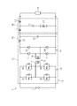
- the vehicle 10 includes a battery 11 and a power conversion device 12.
- the power conversion device 12 includes a DC / DC converter 13, a filter 20, and a filter unit 30.
- the vehicle 10 is an electric vehicle whose drive source is an electric motor or a hybrid vehicle.
- the battery 11 is used as a power source for an electric motor mounted on the vehicle 10.
- a chargeable / discharging power storage device such as a lithium ion secondary battery or a nickel hydrogen storage battery is used.
- the power converter 12 is electrically connected to the load 19 in the home.
- the power conversion device 12 supplies electric power to the load 19 in the home.
- the DC / DC converter 13 includes a bridge circuit 14, a transformer 15, and a rectifier circuit 16.
- the bridge circuit 14 is provided on the primary side of the transformer 15 and includes four switching elements Q1 to Q4.
- the switching elements Q1 and Q2 are connected in series with each other.
- the switching elements Q3 and Q4 are connected in series with each other.
- the rectifier circuit 16 is provided on the secondary side of the transformer 15 and includes four diodes D1 to D4.
- the diodes D1 and D2 are connected in series with each other.
- the diodes D3 and D4 are connected in series with each other.
- the transformer 15 includes a primary winding 17 and a secondary winding 18.
- the primary winding 17 is connected to a connection point between the switching elements Q1 and Q2 and a connection point between the switching elements Q3 and Q4.
- the secondary winding 18 is connected to a connection point between the diodes D1 and D2 and a connection point between the diodes D3 and D4.
- the DC power input from the battery 11 is stepped down by the switching operation of the switching elements Q1 to Q4.
- the switching frequencies of the switching elements Q1 to Q4 are 150 kHz to 200 kHz.
- the DC / DC converter 13 outputs the stepped-down DC power to the filter 20.
- the full-bridge type DC / DC converter 13 is used, but any type of DC / DC converter such as the half-bridge type may be used.
- the filter 20 includes a smoothing coil 21 and a smoothing capacitor 22.
- the filter 20 is an LC filter composed of a smoothing coil 21 and a smoothing capacitor 22.
- the filter 20 attenuates noise in a desired frequency band.
- the smoothing coil 21 smoothes the output power including the ripple rectified by the rectifier circuit 16.
- the filter unit 30 includes a substrate 31, a capacitor C mounted on the substrate 31, and two inductors L1 and L2. Although not shown, the DC / DC converter 13 and the filter 20 are also mounted on the substrate 31.
- the inductors L1 and L2 include a wiring 36 serving as a power line and a core 50.
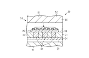
- the substrate 31 includes an insulating layer 32, a pattern 35 to which the capacitor C is connected, and a via 37 to connect the pattern 35 and the wiring 36.
- One of both sides of the insulating layer 32 in the thickness direction is the first surface 33, and the other is the second surface 34.
- the pattern 35 is provided on the first surface 33.
- the wiring 36 is provided on the second surface 34.
- the pattern 35 intersects the wiring 36 when viewed from the thickness direction of the substrate 31.
- As the pattern 35 for example, a copper foil is used.
- a bus bar is used as the wiring 36.
- the capacitor C is connected to the pattern 35 by a bonding material such as solder.
- the insulating layer 32 includes four holes 41 to 44 penetrating in the thickness direction of the substrate 31.
- the position where the pattern 35 and the wiring 36 intersect on the substrate 31 is defined as the intersection X.
- the periphery of the intersection X is divided into four regions A1, A2, A3, and A4 by the pattern 35 and the wiring 36.
- One hole 41 to 44 is provided in each of the four regions A1 to A4.
- the four holes 41 to 44 are arranged on both sides of the pattern 35 and on both sides of the wiring 36, respectively.
- the first hole 41 is one of the four holes 41 to 44.
- the second hole 42 is provided so as to arrange the wiring 36 between the second hole 42 and the first hole 41.
- the third hole 43 is provided so as to arrange the pattern 35 between the third hole 43 and the first hole 41.
- the fourth hole 44 is provided so as to arrange the wiring 36 between the fourth hole 44 and the third hole 43.
- the separation distance between the central axis of the first hole 41 and the central axis of the second hole 42 is the same as the separation distance between the central axis of the third hole 43 and the central axis of the fourth hole 44.
- the separation distance between the central axis of the first hole 41 and the central axis of the third hole 43 is the same as the separation distance between the central axis of the second hole 42 and the central axis of the fourth hole 44.
- Capacitor C is arranged in two places.
- the capacitor C is arranged between the first hole 41 and the third hole 43, and between the second hole 42 and the fourth hole 44.
- a plurality of capacitors C are provided on the pattern 35.
- FIG. 1 shows the combined capacitance of a plurality of capacitors C as one capacitor C.
- the core 50 is divided into two parts.
- a dust core produced by high-pressure press molding of a metallic magnetic powder together with a binder is used.
- any core such as a ferrite core may be used.
- the core 50 includes a first core 51 and a second core 71.
- the first core 51 includes a rectangular plate-shaped pedestal 52 and legs 53 to 56 provided at each of the four corners of the pedestal 52.
- the legs 53 to 56 are columnar.
- the legs 53 to 56 project in the thickness direction of the pedestal 52.
- the legs 53 to 56 project from the pedestal 52 in the same direction.
- the first leg 53 is one of the four legs 53-56.
- the second leg portion 54 is arranged adjacent to the first leg portion 53 in the lateral direction of the pedestal 52.
- the third leg portion 55 is arranged adjacent to the first leg portion 53 in the longitudinal direction of the pedestal 52.
- the fourth leg portion 56 is arranged adjacent to the third leg portion 55 in the lateral direction of the pedestal 52.
- the separation distance between the central axis of the first leg portion 53 and the central axis of the second leg portion 54 is the same as the separation distance between the central axis of the first hole 41 and the central axis of the second hole 42.
- the separation distance between the central axis of the first leg portion 53 and the central axis of the third leg portion 55 is the same as the separation distance between the central axis of the first hole 41 and the central axis of the third hole 43.
- the portion connecting the first leg portion 53 and the second leg portion 54 is referred to as the first connecting portion 61
- the portion connecting the third leg portion 55 and the fourth leg portion 56 is referred to as the second connecting portion 62.
- the first connecting portion 61 includes a portion of the pedestal 52 facing the first leg portion 53, a portion facing the second leg portion 54, and a portion between the first leg portion 53 and the second leg portion 54.
- the second connecting portion 62 includes a portion of the pedestal 52 facing the third leg portion 55, a portion facing the fourth leg portion 56, and a portion between the third leg portion 55 and the fourth leg portion 56.
- the portion connecting the first leg portion 53 and the third leg portion 55 is referred to as the third connecting portion 63
- the portion connecting the second leg portion 54 and the fourth leg portion 56 is referred to as the fourth connecting portion 64.
- the third connecting portion 63 includes a portion of the pedestal 52 facing the first leg portion 53, a portion facing the third leg portion 55, and a portion between the first leg portion 53 and the third leg portion 55.
- the fourth connecting portion 64 includes a portion of the pedestal 52 facing the second leg portion 54, a portion facing the fourth leg portion 56, and a portion between the second leg portion 54 and the fourth leg portion 56.
- the third connecting portion 63 shares a portion of the pedestal 52 facing the first leg portion 53 with the first connecting portion 61.
- the third connecting portion 63 shares a portion of the pedestal 52 facing the third leg portion 55 with the second connecting portion 62.
- the fourth connecting portion 64 shares a portion of the pedestal 52 facing the second leg portion 54 with the first connecting portion 61.
- the fourth connecting portion 64 shares a portion of the pedestal 52 facing the fourth leg portion 56 with the second connecting portion 62.
- the facing portion 65 connects the first connecting portion 61 and the second connecting portion 62.
- a part of the facing portion 65 is a part of the third connecting portion 63 and the fourth connecting portion 64.
- the second core 71 has a square plate shape.
- the second core 71 may have a size that allows all four legs 53 to 56 to come into contact with each other when the second core 71 is overlapped with the first core 51.
- the thickness direction surface of the second core 71 has the same shape as the thickness direction surface of the pedestal 52.
- the first core 51 and the second core 71 are arranged so that the substrate 31 is located between the pedestal 52 and the second core 71.
- the first core 51 is arranged so that the pedestal 52 faces the first surface 33 of the substrate 31.
- the second core 71 is arranged so as to face the second surface 34 of the substrate 31.
- the legs 53 to 56 of the first core 51 are inserted into the holes 41 to 44.
- the first leg 53 is inserted into the first hole 41
- the second leg 54 is inserted into the second hole 42
- the third leg 55 is inserted into the third hole 43
- the fourth leg 56 is inserted into the fourth hole 44.
- Each leg portion 53 to 56 penetrates the insulating layer 32.
- the legs 53 to 56 are in contact with the second core 71.
- the legs 53 to 56 of the first core 51 are in contact with the four corners of the second core 71.
- the second core 71 faces the entire first core 51 while arranging the substrate 31 between the second core 71 and the first core 51.
- the core 50 is composed of the pedestal 52, the legs 53 to 56, and the second core 71. It includes two core bodies 81 and 82.
- One core body 81 is composed of the first leg portion 53, the second leg portion 54, the first connecting portion 61, and the first portion 72 of the second core 71.
- the first portion 72 is a portion of the second core 71 facing the first connecting portion 61 via the substrate 31, the first leg portion 53, and the second leg portion 54.
- One core body 82 is composed of the third leg portion 55, the fourth leg portion 56, the second connecting portion 62, and the second portion 73 of the second core 71.
- the second portion 73 is a portion of the second core 71 facing the second connecting portion 62 via the substrate 31, the third leg portion 55, and the fourth leg portion 56.
- the facing portion 65 connects the core main bodies 81 and 82.
- the second core 71 has a third site 74 between the first site 72 and the second site 73.
- the third portion 74 also connects the core bodies 81 and 82.
- the core bodies 81 and 82 have the same shape.
- the core bodies 81 and 82 are annular and include a wiring hole 83.
- the wiring 36 is passed through the wiring hole 83.
- the core bodies 81 and 82 are arranged so that their central axes face the same direction. The same direction here allows a slight error within the tolerance.
- the wiring 36 passes through the wiring holes 83 of the core bodies 81 and 82 in a straight line.
- the core 50 acts on a magnetic field generated by a current flowing through the wiring 36 to form inductors L1 and L2.
- the inductors L1 and L2 are formed by the wiring 36 and the core bodies 81 and 82, respectively, but it can be considered that one inductor is formed by the wiring 36 and the core 50.
- Each capacitor C is located between the core bodies 81 and 82.
- the capacitor C is located between the first leg 53 and the third leg 55, and between the second leg 54 and the fourth leg 56.
- the facing portion 65 faces the capacitor C in the thickness direction of the substrate 31. It can be said that the thickness direction of the substrate 31 is the direction in which the insulating layer 32 and the pattern 35 overlap.
- the facing portion 65 extends from each of the core main bodies 81 and 82 to a position facing the capacitor C.
- the facing portion 65 faces all of the plurality of capacitors C.
- the capacitor C is sandwiched between the facing portion 65 and the substrate 31 from the thickness direction of the substrate 31.
- the third portion 74 of the second core 71 extends from each of the core main bodies 81 and 82 to a position facing the capacitor C via the substrate 31.
- the third portion 74 of the second core 71 faces all of the plurality of capacitors C via the substrate 31. It can be said that the capacitor C is sandwiched between the facing portion 65 and the third portion 74 from the thickness direction of the substrate 31.
- the core 50 includes two annular portions 91 and 92 composed of a pedestal 52, legs 53 to 56, and a second core 71.
- One annular portion 91 is formed by the first leg portion 53, the third leg portion 55, the third connecting portion 63, and the second core 71.
- the second leg portion 54, the fourth leg portion 56, the fourth connecting portion 64, and the second core 71 constitute one annular portion 92.
- the annular portions 91 and 92 are provided with connection holes 93.
- the connection hole 93 is a hole through which the pattern 35 is passed.
- the annular portions 91 and 92 are arranged so that their central axes face the same direction. The same direction here allows a slight error within the tolerance.
- the direction along the central axis of the annular portions 91 and 92 and the direction along the central axis of the core bodies 81 and 82 are orthogonal to each other.
- the core 50 includes a wiring hole 83 through which the wiring 36 for forming the inductors L1 and L2 passes, and a connection hole 93 through which the pattern 35 for connecting the capacitor C passes.
- the wiring hole 83 has dimensions in the length direction orthogonal to the central axis of the wiring hole 83 and the thickness direction of the substrate 31.
- the connection hole 93 has dimensions in the length direction orthogonal to the central axis of the connection hole 93 and the thickness direction of the substrate 31.
- the length of the wiring hole 83 is smaller than the length of the connection hole 93.
- the filter unit 30 attenuates the noise contained in the DC power output from the filter 20 and outputs the noise.
- the filter unit 30 of the present embodiment attenuates noise in a frequency band of 150 kHz to 200 kHz or less, which is the switching frequency of the switching elements Q1 to Q4, and a frequency band of 500 kHz or more, which is a frequency used for AM broadcasting.
- the electric power output from the filter unit 30 is supplied to the load 19 in the home.
- the inductors L1 and L2 are configured by the wiring 36 and the annular core bodies 81 and 82 surrounding the wiring 36.
- the impedance of the inductors L1 and L2 becomes higher as the frequency becomes higher. Therefore, high frequency noise is cut.
- a magnetic field corresponding to the noise current is generated in the core 50.
- the noise current is converted into a magnetic field and consumed as a magnetic loss. This reduces the noise current.
- the filter unit 30 includes an inductance component L3 due to the capacitor C and the pattern 35.
- the inductors L1 and L2 and the inductance component L3 are magnetically coupled due to the influence of the magnetic field, a voltage is induced. Due to the influence of this voltage, the attenuation characteristic of the filter unit 30 may deteriorate.
- the filter unit 30 of the present embodiment suppresses the magnetic field coupling between the inductors L1 and L2 and the inductance component L3 by suppressing the influence of the magnetic field on the capacitor C.
- the filter unit of the comparative example has the same configuration as the filter unit of the present embodiment except that the shape of the core is different.
- the filter unit 100 of the comparative example includes a core 101.
- the core 101 includes annular core bodies 102 and 103.
- the core 101 is not provided at a position facing the capacitor C in the thickness direction of the substrate 31. That is, in the core 101 used for the filter unit 100 of the comparative example, the facing portion 65 is omitted from the core 50 of the present embodiment.
- FIG. 8 shows the magnetic field distribution generated inside the core 101 of the filter unit 100 of the comparative example when a current flows through the wiring 36.
- the magnetic field distribution indicates the strength of the magnetic field, that is, the magnetic flux density.
- the strength of the magnetic field is represented by dots, and it can be said that the denser the dots, the stronger the strength of the magnetic field.
- the capacitor C is located at a portion where the magnetic field strength is strong, and the inductors L1 and L2 and the inductance component L3 are likely to be magnetically coupled.
- FIG. 9 shows the magnetic field distribution generated inside the core 50 of the filter unit 30 of the present embodiment when a current flows through the wiring 36.
- the facing portion 65 so as to face the capacitor C, the magnetic field at the position where the capacitor C is provided is weakened as compared with the case where the facing portion 65 is not provided. Can be induced.
- the horizontal axis is frequency
- the attenuation characteristics of the filter units 30 and 100 are shown.
- the attenuation characteristics of the filter unit 100 of the comparative example are shown by a alternate long and short dash line
- the attenuation characteristics of the filter unit 30 of the present embodiment are shown by a solid line.
- the attenuation characteristic is lowered at the boundary of 150 kHz to 200 kHz.
- the filter unit 30 of the present embodiment the deterioration of the attenuation characteristic is suppressed even in the band of 150 kHz to 200 kHz or less. In this way, by inducing the magnetic field by the facing portion 65 so that the strength of the magnetic field at the position where the capacitor C is provided is weakened, it is possible to suppress the deterioration of the attenuation characteristics.
- a frequency band for attenuating the noise is set so that the noise contained in the output power from the DC / DC converter 13 does not flow into the home. It may be required to be wide.
- the filter unit 30 of the present embodiment is required to attenuate noise in a frequency band below the switching frequency and a frequency band above the frequency used for AM broadcasting. It is also conceivable to increase the number of filters and the number of capacitors C in order to attenuate noise over a wide frequency band. However, if the number of filters and capacitors C is increased, the size of the power conversion device 12 is increased.
- the attenuation characteristic against noise is improved by changing the magnetic field distribution. Therefore, as compared with the case where the number of filters and the number of capacitors C are increased, the attenuation characteristics of the filter unit 30 are improved while suppressing the increase in size of the power conversion device 12.
- the core 50 includes an opposing portion 65 facing the capacitor C.
- the strength of the magnetic field at the position where the capacitor C is provided can be weakened as compared with the case where the facing portion 65 is not provided.
- By suppressing the influence of the magnetic field on the capacitor C it is possible to suppress the deterioration of the attenuation characteristic of the filter unit 30.
- the pattern 35 intersects the wiring 36 when viewed from the thickness direction of the substrate 31. Since the wiring 36 and the pattern 35 can be arranged so as to be overlapped with each other when viewed from the thickness direction of the substrate 31, the filter unit 30 can be miniaturized.
- the facing portion 65 connects the core main bodies 81 and 82 to each other. By connecting the core bodies 81 and 82 to each other by the facing portion 65, it is easy to induce the magnetic field so that the magnetic field at the position where the capacitor C is provided is weakened.
- the filter unit 30 is an output filter provided on the secondary side of the transformer 15. Since the step-down is performed by the DC / DC converter 13, the current flowing through the secondary side of the transformer 15 is larger than the current flowing through the primary side of the transformer 15. When the current is large, it is difficult to attenuate the noise. By suppressing the deterioration of the attenuation characteristic of the filter unit 30 as in the embodiment, noise can be efficiently attenuated even when the current is large.
- the facing portion 65 does not have to connect the core main bodies 81 and 82 to each other. In this case, the facing portion 65 is provided on one of the core main bodies 81 and 82.
- the core 50 may include any of the core main bodies 81 and 82.
- the capacitor C may be arranged at any position as long as it is around the core bodies 81 and 82.
- the shape of the facing portion 65 may be changed.
- the facing portion 65 may at least face the capacitor C, and a portion that does not face the facing portion 65 may be omitted.
- the shape of the second core 71 may be changed according to the shape of the facing portion 65. It is preferable that the second core 71 is provided at a position facing the facing portion 65 while arranging the substrate 31 between the first core 51 and the second core 71.
- the pattern 35 does not have to intersect the wiring 36 when viewed from the thickness direction of the substrate 31.
- the facing portion 65 may face the capacitor C in a direction orthogonal to both the thickness direction of the substrate 31 and the central axes of the core bodies 81 and 82. That is, the facing portion 65 may extend from the core bodies 81 and 82 to a position facing the capacitor C, and may face the capacitor C in any direction.
- the facing portion 65 may face at least a part of the plurality of capacitors C.
- the core 50 does not have to be divided into a first core 51 and a second core 71.
- the wiring 36 may be wound around the core bodies 81 and 82.
- the filter unit 30 may be used to attenuate noise contained in AC power.
- the filter unit 30 may be provided in any device as long as it is a device that needs to attenuate noise.
Landscapes
- Engineering & Computer Science (AREA)
- Power Engineering (AREA)
- Microelectronics & Electronic Packaging (AREA)
- Manufacturing & Machinery (AREA)
- Filters And Equalizers (AREA)
- Coils Or Transformers For Communication (AREA)
- Fixed Capacitors And Capacitor Manufacturing Machines (AREA)
Abstract
フィルタユニットは、基板と、基板に実装されたコンデンサと、2つのインダクタとを備える。インダクタは、配線と、コアとを備える。コアは、2つのコア本体を備える。コア本体は、環状であり、配線孔を備える。コンデンサは、2つのコア本体の間に配置されている。対向部は、2つのコア本体のそれぞれからコンデンサCに向かい合う位置まで延びている。対向部は、複数のコンデンサの全てに向かい合っている。
Description
本発明は、フィルタユニットに関する。
電子機器は、ノイズを減衰させるためのフィルタを備える。特許文献1に記載のフィルタは、インダクタと、コンデンサとを備える。インダクタは、配線と、配線を囲むコアとを備える。
フィルタを小型化する場合、コンデンサがコアの近くに配置される。配線に電流が流れると、コアにはノイズに基づく磁界が生じる。コンデンサが磁界の影響を受けると、フィルタの減衰特性が低下し得る。
本発明の目的は、ノイズに対する減衰特性の低下を抑制できるフィルタユニットを提供することにある。
上記課題を解決するため、本発明の第一の態様によれば、コンデンサと、配線とコアとを有するインダクタとを備え、前記コアは、前記配線が通される環状のコア本体と、前記コア本体から前記コンデンサに向かい合う位置まで延びる対向部とを備えるフィルタユニットが提供される。
以下、フィルタユニットの一実施形態について説明する。
図1に示すように、車両10は、バッテリ11と、電力変換装置12とを備える。電力変換装置12は、DC/DCコンバータ13と、フィルタ20と、フィルタユニット30とを備える。車両10は、電動機を駆動源とする電動車両や、ハイブリッド車両である。バッテリ11は、車両10に搭載される電動機の電力源として用いられる。バッテリ11としては、例えば、リチウムイオン二次電池やニッケル水素蓄電池等の充放電可能な蓄電装置が用いられる。電力変換装置12は、家庭内の負荷19に電気的に接続される。電力変換装置12は、家庭内の負荷19に電力を供給する。
DC/DCコンバータ13は、ブリッジ回路14と、トランス15と、整流回路16とを備える。ブリッジ回路14は、トランス15の1次側に設けられ、4つのスイッチング素子Q1~Q4を備える。スイッチング素子Q1,Q2は、互いに直列接続されている。スイッチング素子Q3,Q4は、互いに直列接続されている。
整流回路16は、トランス15の2次側に設けられ、4つのダイオードD1~D4を備える。ダイオードD1,D2は、互いに直列接続されている。ダイオードD3,D4は、互いに直列接続されている。
トランス15は、1次側巻線17と、2次側巻線18とを備える。1次側巻線17は、スイッチング素子Q1,Q2同士の接続点と、スイッチング素子Q3,Q4同士の接続点とに接続されている。2次側巻線18は、ダイオードD1,D2同士の接続点と、ダイオードD3,D4同士の接続点とに接続されている。
DC/DCコンバータ13では、スイッチング素子Q1~Q4のスイッチング動作により、バッテリ11から入力された直流電力が降圧される。本実施形態において、スイッチング素子Q1~Q4のスイッチング周波数は、150kHz~200kHzである。DC/DCコンバータ13は、降圧した直流電力をフィルタ20に出力する。本実施形態では、フルブリッジ方式のDC/DCコンバータ13を用いているが、ハーフブリッジ方式等、どのような方式のDC/DCコンバータを用いてもよい。
フィルタ20は、平滑コイル21と、平滑コンデンサ22とを備える。フィルタ20は、平滑コイル21と平滑コンデンサ22によって構成されるLCフィルタである。フィルタ20は、所望の周波数帯域のノイズを減衰させる。平滑コイル21は、整流回路16で整流されたリップルを含む出力電力を平滑する。
図1及び図2に示すように、フィルタユニット30は、基板31と、基板31に実装されたコンデンサCと、2つのインダクタL1,L2とを備える。図示は省略するが、基板31には、DC/DCコンバータ13及びフィルタ20も実装されている。
図2及び図3に示すように、インダクタL1,L2は、電力ラインとなる配線36と、コア50とを備える。基板31は、絶縁層32と、コンデンサCが接続されたパターン35と、パターン35と配線36とを接続するビア37とを備える。絶縁層32の厚み方向の両面のうちの一方を第1面33とし、他方を第2面34とする。パターン35は、第1面33上に設けられている。配線36は、第2面34上に設けられている。基板31の厚み方向から見て、パターン35は、配線36と交差している。パターン35としては、例えば、銅箔が用いられる。配線36としては、バスバーが用いられている。コンデンサCは、半田等の接合材によってパターン35に接続されている。
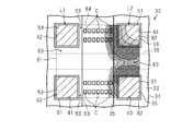
図4に示すように、絶縁層32は、基板31の厚み方向に貫通する4つの孔41~44を備える。基板31の厚み方向から見た場合、基板31において、パターン35と配線36とが交差する位置を交差部Xとする。絶縁層32を基板31の厚み方向から見て、交差部Xの周囲は、パターン35と配線36によって、4つの領域A1,A2,A3,A4に仕切られている。4つの領域A1~A4のそれぞれに、孔41~44は1つずつ設けられている。4つの孔41~44は、パターン35の両側と、配線36の両側とにそれぞれ配置されている。以下の説明において、第1孔41は、4つの孔41~44のうちの1つである。第2孔42は、第2孔42と第1孔41との間に配線36を配置するように設けられている。第3孔43は、第3孔43と第1孔41との間にパターン35を配置するように設けられている。第4孔44は、第4孔44と第3孔43との間に配線36を配置するように設けられている。第1孔41の中心軸と第2孔42の中心軸との離間距離は、第3孔43の中心軸と第4孔44の中心軸との離間距離と同一である。第1孔41の中心軸と第3孔43の中心軸との離間距離は、第2孔42の中心軸と第4孔44の中心軸との離間距離と同一である。
コンデンサCは、2箇所に分かれて配置されている。コンデンサCは、第1孔41と第3孔43との間、及び第2孔42と第4孔44との間に配置されている。図4に示すように、パターン35上には、複数のコンデンサCが設けられている。図1は、複数のコンデンサCの合成容量を1つのコンデンサCとして示している。
図5に示すように、コア50は、2つに分割されている。コア50としては、金属磁性粉末をバインダとともに高圧プレス成型して作製されるダストコアが用いられる。コア50としては、フェライトコア等、どのようなコアを用いてもよい。コア50は、第1コア51と、第2コア71とを備える。第1コア51は、矩形板状の台座52と、台座52の四隅のそれぞれに設けられた脚部53~56とを備える。脚部53~56は、柱状である。脚部53~56は、台座52の厚み方向に突出している。脚部53~56は、台座52から同一方向に突出している。以下の説明において、第1脚部53は、4つの脚部53~56のうちの1つである。第2脚部54は、台座52の短手方向に第1脚部53と隣り合って配置されている。第3脚部55は、台座52の長手方向に第1脚部53と隣り合って配置されている。第4脚部56は、台座52の短手方向に第3脚部55と隣り合って配置されている。第1脚部53の中心軸と第2脚部54の中心軸との離間距離は、第1孔41の中心軸と第2孔42の中心軸との離間距離と同一である。第1脚部53の中心軸と第3脚部55の中心軸との離間距離は、第1孔41の中心軸と第3孔43の中心軸との離間距離と同一である。
台座52において、第1脚部53と第2脚部54とを連結する部分を第1連結部61とし、第3脚部55と第4脚部56とを連結する部分を第2連結部62とする。第1連結部61は、台座52において、第1脚部53に向かい合う部分、第2脚部54に向かい合う部分、及び第1脚部53と第2脚部54との間の部分を含む。第2連結部62は、台座52において、第3脚部55に向かい合う部分、第4脚部56に向かい合う部分、及び第3脚部55と第4脚部56との間の部分を含む。
台座52において、第1脚部53と第3脚部55とを連結する部分を第3連結部63とし、第2脚部54と第4脚部56とを連結する部分を第4連結部64とする。第3連結部63は、台座52において、第1脚部53に向かい合う部分、第3脚部55に向かい合う部分、及び第1脚部53と第3脚部55との間の部分を含む。第4連結部64は、台座52において、第2脚部54に向かい合う部分、第4脚部56に向かい合う部分、及び第2脚部54と第4脚部56との間の部分を含む。第3連結部63は、台座52において、第1脚部53に向かい合う部分を第1連結部61と共有している。第3連結部63は、台座52において、第3脚部55に向かい合う部分を第2連結部62と共有している。第4連結部64は、台座52において、第2脚部54に向かい合う部分を第1連結部61と共有している。第4連結部64は、台座52において、第4脚部56に向かい合う部分を第2連結部62と共有している。
台座52において、第1連結部61と第2連結部62との間の部分を対向部65とすると、対向部65は、第1連結部61と第2連結部62とを連結している。対向部65の一部は、第3連結部63及び第4連結部64の一部となっている。
第2コア71は、四角板状である。第2コア71は、第1コア51と重ねたときに4つの脚部53~56の全てが接触できる大きさを有していればよい。本実施形態において、第2コア71の厚み方向の面は、台座52の厚み方向の面と同一形状である。
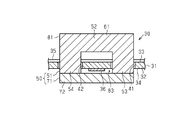
図2、図4及び図6に示すように、第1コア51と第2コア71とは、台座52と第2コア71との間に基板31が位置するように配置されている。第1コア51は、台座52を基板31の第1面33と向かい合わせるように配置されている。第2コア71は、基板31の第2面34と向かい合うように配置されている。第1コア51の各脚部53~56は、各孔41~44に挿入されている。第1脚部53は第1孔41、第2脚部54は第2孔42、第3脚部55は第3孔43、第4脚部56は第4孔44にそれぞれ挿入されている。各脚部53~56は、絶縁層32を貫通している。各脚部53~56は、第2コア71に接触している。詳細には、第1コア51の各脚部53~56は、第2コア71の四隅に接触している。第2コア71は、第2コア71と第1コア51との間に基板31を配置しつつ、第1コア51の全体に向かい合っている。
図2及び図6に示すように、各脚部53~56が第2コア71に接触することで、コア50は、台座52、各脚部53~56及び第2コア71によって構成される2つのコア本体81,82を備える。第1脚部53、第2脚部54、第1連結部61、及び第2コア71の第1部位72によって、1つのコア本体81が構成されている。第1部位72は、第2コア71において、基板31、第1脚部53及び第2脚部54を介して第1連結部61に向かい合う部分である。第3脚部55、第4脚部56、第2連結部62、及び第2コア71の第2部位73によって、1つのコア本体82が構成されている。第2部位73は、第2コア71において、基板31、第3脚部55及び第4脚部56を介して第2連結部62に向かい合う部分である。対向部65は、コア本体81,82を連結している。第2コア71は、第1部位72と第2部位73との間に第3部位74を有している。第3部位74も、コア本体81,82を連結している。
本実施形態において、コア本体81,82は同一形状である。コア本体81,82は、環状であり、配線孔83を備える。配線孔83には、配線36が通される。コア本体81,82は、中心軸が同一方向を向くように配置されている。ここでいう同一方向とは、公差の範囲内での若干の誤差を許容する。
配線36は、コア本体81,82の配線孔83を直線状に通過している。コア50は、配線36を流れる電流によって発生する磁界に作用して、インダクタL1,L2を構成する。本実施形態では、配線36とコア本体81,82のそれぞれとによってインダクタL1,L2が構成されているが、配線36とコア50とにより1つのインダクタが構成されていると捉えることもできる。
各コンデンサCは、コア本体81,82の間に位置している。コンデンサCは、第1脚部53と第3脚部55との間、及び第2脚部54と第4脚部56との間に位置している。対向部65は、基板31の厚み方向にコンデンサCと向かい合っている。基板31の厚み方向は、絶縁層32とパターン35が重なる方向ともいえる。対向部65は、コア本体81,82のそれぞれからコンデンサCに向かい合う位置まで延びている。対向部65は、複数のコンデンサCのうちの全てに向かい合っている。コンデンサCは、基板31の厚み方向から、対向部65と基板31とによって挟まれている。
第2コア71の第3部位74は、コア本体81,82のそれぞれから基板31を介してコンデンサCに向かい合う位置まで延びている。第2コア71の第3部位74は、基板31を介して複数のコンデンサCのうちの全てに向かい合っている。コンデンサCは、基板31の厚み方向から、対向部65と第3部位74とによって挟まれているといえる。
図2及び図4に示すように、コア50は、台座52、各脚部53~56及び第2コア71によって構成される2つの環状部91,92を備える。第1脚部53、第3脚部55、第3連結部63、及び第2コア71によって、1つの環状部91が構成されている。第2脚部54、第4脚部56、第4連結部64、及び第2コア71によって、1つの環状部92が構成されている。
環状部91,92は、接続孔93を備える。接続孔93は、パターン35が通される孔である。環状部91,92は、中心軸が同一方向を向くように配置されている。ここでいう同一方向とは、公差の範囲内での若干の誤差を許容する。環状部91,92の中心軸に沿う方向と、コア本体81,82の中心軸に沿う方向とは、互いに直交する。コア50は、インダクタL1,L2を構成するための配線36が通る配線孔83と、コンデンサCを接続するためのパターン35が通る接続孔93とを備えている。配線孔83は、配線孔83の中心軸及び基板31の厚み方向に直交する長さ方向の寸法を有している。接続孔93は、接続孔93の中心軸及び基板31の厚み方向に直交する長さ方向の寸法を有している。配線孔83の長さは、接続孔93の長さよりも小さい。
フィルタユニット30は、フィルタ20から出力された直流電力に含まれるノイズを減衰させて出力する。本実施形態のフィルタユニット30は、スイッチング素子Q1~Q4のスイッチング周波数である150kHz~200khz以下の周波数帯域、及びAM放送に用いられる周波数である500kHz以上の周波数帯域のノイズを減衰させる。フィルタユニット30から出力される電力は、家庭内の負荷19に供給される。
本実施形態の作用について説明する。
配線36と、配線36を囲む環状のコア本体81,82とによって、インダクタL1,L2が構成される。インダクタL1,L2のインピーダンスは、周波数が高くなるほど、高くなる。このため、高周波のノイズがカットされる。
また、配線36に高周波のノイズ電流が流れると、コア50内にノイズ電流に対応した磁界が生じる。ノイズ電流は磁界に変換され、磁気損失として消費される。これにより、ノイズ電流が低減される。
図1に示すように、フィルタユニット30は、コンデンサCやパターン35に起因するインダクタンス成分L3を備える。磁界の影響によって、インダクタL1,L2とインダクタンス成分L3とが磁界結合すると、電圧が誘起される。この電圧の影響により、フィルタユニット30の減衰特性が低下する場合がある。本実施形態のフィルタユニット30は、磁界がコンデンサCに与える影響を抑制することで、インダクタL1,L2とインダクタンス成分L3との磁界結合を抑制している。以下、詳細に説明を行う。
まず、比較例のフィルタユニットについて説明する。比較例のフィルタユニットは、コアの形状が異なることを除いて、本実施形態のフィルタユニットと同一の構成を備える。
図7に示すように、比較例のフィルタユニット100は、コア101を備える。コア101は、環状のコア本体102,103を備える。基板31の厚み方向にコンデンサCと向かい合う位置には、コア101が設けられていない。即ち、比較例のフィルタユニット100に用いられるコア101では、本実施形態のコア50から対向部65が省略されている。
図8は、配線36に電流が流れた場合に比較例のフィルタユニット100のコア101の内部に生じる磁界分布を示している。磁界分布は、磁界の強さの強弱、即ち、磁束密度を示している。図8では、磁界の強さの強弱をドットで表現しており、ドットが密である部分ほど磁界の強さが強いといえる。図8から把握できるように、比較例のフィルタユニット100では、磁界の強さの強い部分にコンデンサCが位置しており、インダクタL1,L2とインダクタンス成分L3とが磁界結合しやすい。
図9は、配線36に電流が流れた場合に本実施形態のフィルタユニット30のコア50の内部に生じる磁界分布を示している。図9から把握できるように、コンデンサCに向かい合うように対向部65を設けることで、対向部65を設けない場合に比べて、コンデンサCが設けられる位置の磁界の強さが弱くなるように磁界を誘導することができる。
図10は、縦軸を利得=減衰率とし、横軸を周波数とし、フィルタユニット30,100の減衰特性を示している。比較例のフィルタユニット100の減衰特性を一点鎖線で示し、本実施形態のフィルタユニット30の減衰特性を実線で示している。比較例のフィルタユニット100では、150kHz~200kHzを境に減衰特性が低下している。これに対し、本実施形態のフィルタユニット30では、150kHz~200kHz以下の帯域でも減衰特性の低下が抑制されている。このように、対向部65により磁界を誘導し、コンデンサCが設けられる位置の磁界の強さが弱くなるようにすることで、減衰特性の低下を抑制できる。
DC/DCコンバータ13からの出力電力が家庭内の負荷19に供給される場合、DC/DCコンバータ13からの出力電力に含まれるノイズが家庭内に流入しないように、ノイズを減衰させる周波数帯域を広くすることが求められることがある。本実施形態のフィルタユニット30には、スイッチング周波数以下の周波数帯域、及びAM放送に用いられる周波数以上の周波数帯域のノイズを減衰することが求められている。広い周波数帯域に亘ってノイズを減衰させるため、フィルタの数やコンデンサCの数を増加させることも考えられる。しかしながら、フィルタやコンデンサCの数を多くした場合、電力変換装置12の大型化を招く。これに対し、本実施形態では、磁界分布を変更することで、ノイズに対する減衰特性が向上する。従って、フィルタの数やコンデンサCの数を多くする場合に比べて、電力変換装置12の大型化を抑制しつつフィルタユニット30の減衰特性が向上する。
本実施形態の効果について説明する。
(1)コア50は、コンデンサCに向かい合う対向部65を備える。対向部65により磁界を誘導することで、対向部65を設けない場合に比べて、コンデンサCが設けられる位置の磁界の強さを弱くできる。磁界によるコンデンサCへの影響を抑制することで、フィルタユニット30の減衰特性が低下することを抑制できる。
(2)基板31の厚み方向から見て、パターン35は、配線36と交差している。基板31の厚み方向から見て、配線36とパターン35とを重ねて配置できるため、フィルタユニット30の小型化が図られる。
(3)2つのコア本体81,82を設け、コンデンサCは、コア本体81,82の間に配置されている。この配置によれば、2つのコア本体81,82の間を、コンデンサCを配置するための領域として利用することができる。よって、コンデンサCを2つのコア本体81,82の間とは異なる位置に配置する場合に比べて、フィルタユニット30の小型化が図られる。
(4)対向部65は、コア本体81,82同士を連結している。対向部65によりコア本体81,82同士を連結することで、コンデンサCが設けられる位置の磁界が弱くなるように磁界を誘導しやすい。
(5)フィルタユニット30は、トランス15の二次側に設けられた出力フィルタである。DC/DCコンバータ13で降圧を行っているため、トランス15の二次側を流れる電流は、トランス15の一次側を流れる電流に比べて大きくなる。電流が大きいと、ノイズの減衰を行いにくい。実施形態のように、フィルタユニット30の減衰特性の低下を抑制することで、電流が大きい場合であっても、効率よくノイズを減衰させることができる。
実施形態は、以下のように変更して実施することができる。実施形態及び以下の変形例は、技術的に矛盾しない範囲で互いに組み合わせて実施することができる。
対向部65は、コア本体81,82同士を連結していなくてもよい。この場合、対向部65は、コア本体81,82のうちの一方に設けられる。
コア50は、コア本体81,82のうちいずれかを備えていればよい。この場合、コンデンサCは、コア本体81,82の周囲であれば、どのような位置に配置されてもよい。
対向部65の形状は、変更してもよい。対向部65は、少なくとも、コンデンサCに向かい合っていればよく、対向部65と向かい合わない部分を省略してもよい。対向部65の形状を変更する場合、対向部65の形状に合わせて第2コア71の形状を変更してもよい。第2コア71は、第1コア51と第2コア71との間に基板31を配置しつつ、対向部65と向かい合う位置に設けられていることが好ましい。
基板31の厚み方向から見て、パターン35は、配線36と交差していなくてもよい。
対向部65は、基板31の厚み方向及びコア本体81,82の中心軸の両方に直交する方向にコンデンサCと向かい合っていてもよい。即ち、対向部65は、コア本体81,82からコンデンサCと向かい合う位置まで延びていればよく、いずれの方向にコンデンサCと向かい合っていてもよい。
対向部65は、複数のコンデンサCのうち少なくとも一部に向かい合っていればよい。
コア50は、第1コア51と第2コア71とに分割されていなくてもよい。
配線36は、コア本体81,82に巻回されていてもよい。
フィルタユニット30は、交流電力に含まれるノイズを減衰するために用いてもよい。
フィルタユニット30は、ノイズを減衰させる必要のある機器であれば、どのような機器に設けられてもよい。
Claims (5)
- コンデンサと、
配線とコアとを有するインダクタとを備え、
前記コアは、
前記配線が通される環状のコア本体と、
前記コア本体から前記コンデンサに向かい合う位置まで延びる対向部と
を備える、フィルタユニット。 - 前記コンデンサが実装された基板を備え、
前記対向部は、前記基板の厚み方向に前記コンデンサと向かい合う、請求項1に記載のフィルタユニット。 - 前記基板は、前記コンデンサが接続されるパターンを備え、
前記基板の厚み方向から見て、前記パターンは、前記配線と交差している、請求項2に記載のフィルタユニット。 - 前記コア本体は、2つのコア本体のうちの一つであり、
前記コンデンサは、前記2つのコア本体の間に配置される、請求項1~請求項3のうちいずれか一項に記載のフィルタユニット。 - 前記対向部は、前記2つのコア本体を連結している、請求項4に記載のフィルタユニット。
Priority Applications (3)
| Application Number | Priority Date | Filing Date | Title |
|---|---|---|---|
| DE112020003040.7T DE112020003040T5 (de) | 2019-06-27 | 2020-06-11 | Filtereinheit |
| CN202080045842.2A CN114008916B (zh) | 2019-06-27 | 2020-06-11 | 滤波器单元 |
| US17/597,014 US11990886B2 (en) | 2019-06-27 | 2020-06-11 | Filter unit |
Applications Claiming Priority (2)
| Application Number | Priority Date | Filing Date | Title |
|---|---|---|---|
| JP2019120321A JP7226139B2 (ja) | 2019-06-27 | 2019-06-27 | フィルタユニット |
| JP2019-120321 | 2019-06-27 |
Publications (1)
| Publication Number | Publication Date |
|---|---|
| WO2020262013A1 true WO2020262013A1 (ja) | 2020-12-30 |
Family
ID=74060383
Family Applications (1)
| Application Number | Title | Priority Date | Filing Date |
|---|---|---|---|
| PCT/JP2020/022982 Ceased WO2020262013A1 (ja) | 2019-06-27 | 2020-06-11 | フィルタユニット |
Country Status (5)
| Country | Link |
|---|---|
| US (1) | US11990886B2 (ja) |
| JP (1) | JP7226139B2 (ja) |
| CN (1) | CN114008916B (ja) |
| DE (1) | DE112020003040T5 (ja) |
| WO (1) | WO2020262013A1 (ja) |
Citations (3)
| Publication number | Priority date | Publication date | Assignee | Title |
|---|---|---|---|---|
| JPH0351518U (ja) * | 1989-09-27 | 1991-05-20 | ||
| JPH11127579A (ja) * | 1997-08-04 | 1999-05-11 | Alcatel Cit | 磁気回路に組み込まれた電力コンバータ |
| JP2016100348A (ja) * | 2014-11-18 | 2016-05-30 | 北川工業株式会社 | 出力ノイズ低減装置 |
Family Cites Families (12)
| Publication number | Priority date | Publication date | Assignee | Title |
|---|---|---|---|---|
| JPH0186715U (ja) * | 1987-11-30 | 1989-06-08 | ||
| JPH02143828U (ja) * | 1989-05-08 | 1990-12-06 | ||
| JPH0565117U (ja) * | 1992-02-14 | 1993-08-27 | 太陽誘電株式会社 | チップ型ノイズ除去フィルタ |
| JP3680627B2 (ja) * | 1999-04-27 | 2005-08-10 | 富士電機機器制御株式会社 | ノイズフィルタ |
| JP4222197B2 (ja) * | 2003-02-24 | 2009-02-12 | 株式会社村田製作所 | 弾性表面波フィルタ、通信機 |
| JP2006179596A (ja) * | 2004-12-21 | 2006-07-06 | Mitsubishi Electric Corp | 半導体装置 |
| JP6114660B2 (ja) | 2013-08-23 | 2017-04-12 | 日立オートモティブシステムズ株式会社 | 電力変換装置 |
| US9711279B2 (en) | 2013-10-28 | 2017-07-18 | Infineon Technologies Austria Ag | DC-DC converter assembly with an output inductor accommodating a power stage attached to a circuit board |
| JP6307937B2 (ja) | 2014-03-03 | 2018-04-11 | 株式会社オートネットワーク技術研究所 | ノイズフィルタ |
| JP6379401B2 (ja) | 2014-09-11 | 2018-08-29 | 北川工業株式会社 | 出力ノイズ低減装置 |
| CN107408931B (zh) * | 2015-07-28 | 2020-06-19 | 株式会社村田制作所 | 电路基板、使用其的滤波器电路以及电容器元件 |
| US10991665B2 (en) * | 2016-09-29 | 2021-04-27 | Intel Corporation | Package-level noise filtering for EMI RFI mitigation |
-
2019
- 2019-06-27 JP JP2019120321A patent/JP7226139B2/ja active Active
-
2020
- 2020-06-11 CN CN202080045842.2A patent/CN114008916B/zh active Active
- 2020-06-11 WO PCT/JP2020/022982 patent/WO2020262013A1/ja not_active Ceased
- 2020-06-11 US US17/597,014 patent/US11990886B2/en active Active
- 2020-06-11 DE DE112020003040.7T patent/DE112020003040T5/de active Pending
Patent Citations (3)
| Publication number | Priority date | Publication date | Assignee | Title |
|---|---|---|---|---|
| JPH0351518U (ja) * | 1989-09-27 | 1991-05-20 | ||
| JPH11127579A (ja) * | 1997-08-04 | 1999-05-11 | Alcatel Cit | 磁気回路に組み込まれた電力コンバータ |
| JP2016100348A (ja) * | 2014-11-18 | 2016-05-30 | 北川工業株式会社 | 出力ノイズ低減装置 |
Also Published As
| Publication number | Publication date |
|---|---|
| CN114008916A (zh) | 2022-02-01 |
| US20220321084A1 (en) | 2022-10-06 |
| US11990886B2 (en) | 2024-05-21 |
| JP7226139B2 (ja) | 2023-02-21 |
| CN114008916B (zh) | 2025-08-05 |
| JP2021005691A (ja) | 2021-01-14 |
| DE112020003040T5 (de) | 2022-05-05 |
Similar Documents
| Publication | Publication Date | Title |
|---|---|---|
| JP6038385B2 (ja) | デュアルモードチョークコイル及びそれを用いた高周波フィルタ並びに車載用モータ一体型電動パワーステアリング及び車載用充電装置 | |
| CN109494974B (zh) | 用于抑制干扰信号的电磁兼容性滤波器 | |
| JPWO2011154993A1 (ja) | 絶縁トランスおよび電源装置 | |
| JP2013027077A (ja) | 電力変換装置 | |
| JPWO2014155873A1 (ja) | 積層型コイル部品および整合回路 | |
| TW201628031A (zh) | 電源裝置、磁性元件及其繞組單元 | |
| JP6330311B2 (ja) | 巻線部品及び電源装置 | |
| JP6975902B2 (ja) | Llc共振コンバーター | |
| JP6326803B2 (ja) | コイル基板、巻線部品及び電源装置 | |
| JP6344540B2 (ja) | 電力変換モジュール | |
| JP2024529793A (ja) | 平面トランス用のプリント回路基板の集積共振能力 | |
| JP2018098853A (ja) | シールド、電子回路、及び、dc−dcコンバータ | |
| JP7226139B2 (ja) | フィルタユニット | |
| JP2015061361A (ja) | 電力変換装置 | |
| JP6255990B2 (ja) | 巻線部品 | |
| JP3823322B2 (ja) | 分布定数構造 | |
| JP2019009177A (ja) | 磁性被覆コイル及びこれを用いたトランス | |
| TWI625744B (zh) | 三相耦合電感 | |
| WO2020026640A1 (ja) | インダクタ、複合インダクタ、dc/dcコンバータ及び回路 | |
| JP6364765B2 (ja) | 巻線部品 | |
| JP6439319B6 (ja) | 巻線部および巻線部品 | |
| JP2011243829A (ja) | 積層型電子部品 | |
| JP2012099512A (ja) | 複合電子部品 | |
| JP2012079918A (ja) | チョークコイル | |
| JP5273817B2 (ja) | 力率改善回路の昇圧用コイルとそれを備えるac−dcコンバータ |
Legal Events
| Date | Code | Title | Description |
|---|---|---|---|
| 121 | Ep: the epo has been informed by wipo that ep was designated in this application |
Ref document number: 20832547 Country of ref document: EP Kind code of ref document: A1 |
|
| 122 | Ep: pct application non-entry in european phase |
Ref document number: 20832547 Country of ref document: EP Kind code of ref document: A1 |
|
| WWG | Wipo information: grant in national office |
Ref document number: 202080045842.2 Country of ref document: CN |