WO2020262015A1 - Substrat métal-céramique assemblé et son procédé de fabrication - Google Patents
Substrat métal-céramique assemblé et son procédé de fabrication Download PDFInfo
- Publication number
- WO2020262015A1 WO2020262015A1 PCT/JP2020/022998 JP2020022998W WO2020262015A1 WO 2020262015 A1 WO2020262015 A1 WO 2020262015A1 JP 2020022998 W JP2020022998 W JP 2020022998W WO 2020262015 A1 WO2020262015 A1 WO 2020262015A1
- Authority
- WO
- WIPO (PCT)
- Prior art keywords
- metal
- aluminum
- graphite sheet
- substrate
- ceramic
- Prior art date
- Legal status (The legal status is an assumption and is not a legal conclusion. Google has not performed a legal analysis and makes no representation as to the accuracy of the status listed.)
- Ceased
Links
Images


Classifications
-
- H—ELECTRICITY
- H05—ELECTRIC TECHNIQUES NOT OTHERWISE PROVIDED FOR
- H05K—PRINTED CIRCUITS; CASINGS OR CONSTRUCTIONAL DETAILS OF ELECTRIC APPARATUS; MANUFACTURE OF ASSEMBLAGES OF ELECTRICAL COMPONENTS
- H05K1/00—Printed circuits
- H05K1/02—Details
- H05K1/0201—Thermal arrangements, e.g. for cooling, heating or preventing overheating
- H05K1/0203—Cooling of mounted components
-
- H—ELECTRICITY
- H10—SEMICONDUCTOR DEVICES; ELECTRIC SOLID-STATE DEVICES NOT OTHERWISE PROVIDED FOR
- H10W—GENERIC PACKAGES, INTERCONNECTIONS, CONNECTORS OR OTHER CONSTRUCTIONAL DETAILS OF DEVICES COVERED BY CLASS H10
- H10W40/00—Arrangements for thermal protection or thermal control
- H10W40/20—Arrangements for cooling
- H10W40/25—Arrangements for cooling characterised by their materials
- H10W40/255—Arrangements for cooling characterised by their materials having a laminate or multilayered structure, e.g. direct bond copper [DBC] ceramic substrates
-
- H—ELECTRICITY
- H10—SEMICONDUCTOR DEVICES; ELECTRIC SOLID-STATE DEVICES NOT OTHERWISE PROVIDED FOR
- H10W—GENERIC PACKAGES, INTERCONNECTIONS, CONNECTORS OR OTHER CONSTRUCTIONAL DETAILS OF DEVICES COVERED BY CLASS H10
- H10W70/00—Package substrates; Interposers; Redistribution layers [RDL]
- H10W70/01—Manufacture or treatment
- H10W70/02—Manufacture or treatment of conductive package substrates serving as an interconnection, e.g. of metal plates
-
- H—ELECTRICITY
- H10—SEMICONDUCTOR DEVICES; ELECTRIC SOLID-STATE DEVICES NOT OTHERWISE PROVIDED FOR
- H10W—GENERIC PACKAGES, INTERCONNECTIONS, CONNECTORS OR OTHER CONSTRUCTIONAL DETAILS OF DEVICES COVERED BY CLASS H10
- H10W99/00—Subject matter not provided for in other groups of this subclass
-
- H—ELECTRICITY
- H10—SEMICONDUCTOR DEVICES; ELECTRIC SOLID-STATE DEVICES NOT OTHERWISE PROVIDED FOR
- H10W—GENERIC PACKAGES, INTERCONNECTIONS, CONNECTORS OR OTHER CONSTRUCTIONAL DETAILS OF DEVICES COVERED BY CLASS H10
- H10W40/00—Arrangements for thermal protection or thermal control
- H10W40/20—Arrangements for cooling
- H10W40/25—Arrangements for cooling characterised by their materials
Definitions
- the present invention relates to a metal-ceramics bonded substrate and a method for manufacturing the same.
- a metal plate (metal circuit board) for mounting electronic components is formed on one surface of the ceramics substrate, and a metal base plate for heat dissipation is formed on the other surface.
- the present invention relates to a metal-ceramics bonded substrate on which the above is formed and a method for manufacturing the same.
- a metal-ceramic circuit board in which a metal circuit board made of aluminum or an aluminum alloy is directly bonded to the ceramic substrate has been used in order to realize higher thermal cycle resistance. ..
- the ceramics board having a small linear expansion coefficient and the metal circuit board made of aluminum or an aluminum alloy having a large linear expansion coefficient are directly bonded to each other. Due to the stress generated by the difference in linear expansion coefficient, the aluminum or aluminum alloy is plastically deformed, and a large wrinkle-like deformation (step) occurs in the portion corresponding to the crystal grain boundary of the aluminum or aluminum alloy, resulting in the metal circuit board. There is a risk that the soldered semiconductor element will be damaged, cracks will occur in the solder, and the bonding wire that connects the semiconductor element to the metal circuit board will peel off.
- an insulating substrate for semiconductor mounting in which an alloy metal layer having a Vickers hardness HV of 25 or more (mainly aluminum) is formed on the ceramic substrate, or a ceramic substrate
- a metal-ceramic circuit board in which a metal film made of copper or a copper alloy is formed by a cold spray method on a formed metal circuit board made of aluminum or an aluminum alloy, or directly on the ceramics substrate.
- a metal-ceramics circuit board in which a nickel plating film having a thickness of 17 ⁇ m or more is formed on the surface of a metal circuit board made of bonded aluminum has been proposed.
- JP-A-2007-36263 (paragraph number 0014) JP-A-2016-152324 (paragraph number 0009-0011) Japanese Unexamined Patent Publication No. 2018-18992 (paragraph number 0009-0010)
- the present invention considers aluminum or aluminum even if a heat cycle is repeatedly applied to a metal-ceramics bonded substrate in which a metal circuit board made of aluminum or an aluminum alloy is directly bonded to a ceramics substrate. It is an object of the present invention to provide an inexpensive metal-ceramics bonded substrate and a method for manufacturing the same, which can prevent a large step from being generated in a portion corresponding to the crystal grain boundary of the alloy.
- the present inventors have made aluminum or an aluminum alloy on the other surface of a ceramics substrate in which one surface is directly bonded to the metal base plate of a metal base plate made of aluminum or an aluminum alloy.
- One surface of a first metal plate made of is directly bonded, one surface of a graphite sheet is directly bonded to the other surface of the first metal plate, and aluminum or an aluminum alloy is bonded to the other surface of the graphite sheet.
- the metal-ceramics bonded substrate according to the present invention includes a metal base plate made of aluminum or an aluminum alloy, a ceramics substrate in which one surface is directly bonded to the metal base plate, and one surface to the other surface of the ceramics substrate.
- the graphite sheet extends substantially parallel to the bonding surface of the first metal plate with the ceramic substrate, and is substantially parallel to the bonding surface of the first metal plate with the ceramic substrate. It is preferable that it extends over substantially the entire surface of the flat surface. Further, it is preferable that the end face of the graphite sheet is exposed to the outside. Further, it is preferable that the circuit pattern is formed by the first metal plate, the graphite sheet and the second metal plate.
- the end portion of the graphite sheet and the end portion of the ceramics substrate are used as a mold so that the graphite sheet and the ceramics substrate are separated and arranged substantially in parallel in the mold.
- a metal base plate made of aluminum or aluminum alloy is formed by pouring molten aluminum or aluminum alloy into the mold so that it is supported and in contact with both sides of the graphite sheet and both sides of the ceramic substrate, and then cooling and solidifying. Then, it is directly bonded to one surface of the ceramic substrate to form a first metal plate made of aluminum or an aluminum alloy and directly bonded to one surface of the graphite sheet and the other surface of the ceramic plate, and aluminum or aluminum. It is characterized in that a second metal plate made of an alloy is formed and directly bonded to the other surface of the graphite sheet.
- the mask, the second metal plate, and the graphite sheet are formed in the thickness direction from the surface of the mask.
- a circuit pattern shape is formed except for a portion other than the portion corresponding to the circuit pattern shape of the first metal plate, which is removed by milling to leave a part of the first metal plate on the ceramic substrate side, and then the ceramic substrate is formed.
- the mask is removed to obtain a circuit pattern composed of the first metal plate, the graphite sheet, and the second metal plate. It is preferable to form.
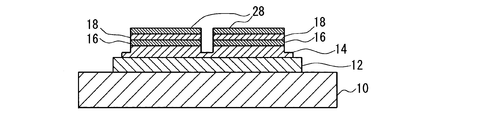
- a metal base plate 10 made of aluminum or an aluminum alloy having a substantially rectangular planar shape and one surface directly on the metal base plate 10
- a ceramic substrate 12 having a substantially rectangular planar shape that has been joined (chemically joined with sufficient bonding strength) and one surface are directly bonded to the other surface of the ceramic substrate 12 (chemically bonded with sufficient bonding strength).
- a first metal plate 14 for a circuit pattern made of aluminum or an aluminum alloy having a substantially rectangular planar shape and one surface are directly bonded to the other surface of the first metal plate 14 (chemical with sufficient bonding strength).
- a substantially rectangular graphite sheet 16 (having substantially the same size as the first metal plate 14) and a direct bond (chemically with sufficient bonding strength) to the other surface of the graphite sheet 16. It is provided with a second metal plate 18 for a circuit pattern made of aluminum or an aluminum alloy having a substantially rectangular shape (having substantially the same size as the graphite sheet 16). Further, the graphite sheet 16 extends over substantially the entire surface of a (virtual) plane substantially parallel to the joint surface of the first metal plate 14 with the ceramic substrate 12 and substantially parallel to the joint surface, and is an edge of the graphite sheet 16. The part is exposed to the outside (preferably over the entire circumference).
- the thickness is 10 to 1000 ⁇ m (preferably 30 to 120 ⁇ m)
- the thermal conductivity in the horizontal direction is 250 to 2000 W / m ⁇ K (preferably 900 to 2000 W / m ⁇ K)
- the thermal conductivity in the thickness direction is 250 to 2000 W / m ⁇ K.
- a sheet (plate material) made of graphite having a linear expansion coefficient of 2 to 10 ppm / K (preferably 4 to 7 ppm / K) and a linear expansion coefficient of 10 to 30 W / m ⁇ K (preferably 18 to 30 W / m ⁇ K) can be used. ..
- the surface distortion (deformation) of the surface of the second metal plate 18 for the circuit pattern is caused. It can be suppressed, wrinkles can be suppressed on the surface of the second metal plate 18 for the circuit pattern after the heat cycle, and the ceramic substrate 12 and (on the second metal plate 18) can be suppressed by the heat cycle. It is possible to prevent cracks from occurring in the mounted semiconductor element or the like and reduce the manufacturing cost, and it is possible to manufacture a metal-ceramics bonded substrate having excellent heat conduction and electrical conduction. Further, by arranging the second metal plate 18 on the outermost surface, it is possible to plate the surface, perform ultrasonic bonding with an aluminum wire, a copper wire, or the like, or perform ultrasonic bonding of copper terminals. ..
- the peripheral portion of the ceramic substrate 12 and the graphite sheet 16 are arranged so that the ceramic substrate 12 and the graphite sheet 16 are separated from each other in the mold 20 shown in FIG.
- the peripheral portion of the mold 20 is supported by the mold 20, and the inside of the mold 20 is heated in a nitrogen atmosphere so that both sides of the ceramic substrate 12 in the mold 20 and both sides of the graphite sheet 16 are contacted with aluminum or an aluminum alloy.
- the molten metal can be produced by pouring the molten metal while removing the oxide film on its surface, and then cooling the mold 20 to solidify the molten metal.
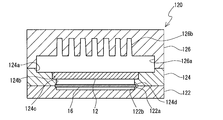
- the mold 20 is made of carbon or the like, and is composed of a lower mold member 22 having a substantially rectangular planar shape, an intermediate mold member 24, and an upper mold member 26, respectively.
- the upper surface of the lower mold member 22 has a graphite sheet having substantially the same shape and size as the portion of the graphite sheet 16 on the second metal plate 18 side (approximately half in the present embodiment).
- a recess (graphite sheet accommodating portion) 22a for accommodating a portion of 16 on the side of the second metal plate 18 is formed, and a recess (second) for accommodating the second metal plate 18 is formed on the bottom surface of the recess 22a. 2 metal plate forming portion) 22b is formed.
- a recess (metal base plate forming portion) 24a for forming a portion (a part of the metal base plate 10) of the metal base plate 10 on the ceramic substrate 12 side is formed on the upper surface of the intermediate mold member 24, and the recess 24a is formed.
- a recess (ceramic substrate accommodating portion) 24b for accommodating the ceramic substrate 12 is formed on the bottom surface in substantially the same shape and size as the ceramic substrate 12, and the first metal plate 14 is formed on the bottom surface of the recess 24b.
- a through hole (first metal plate forming portion) 24c for forming the first metal plate 14 is formed with substantially the same shape and size as the above.
- the graphite sheet 16 has substantially the same shape and size as the portion of the graphite sheet 16 on the first metal plate 14 side (approximately half in the present embodiment).
- a recess (graphite sheet accommodating portion) 24d for accommodating the portion of 1 on the metal plate 14 side is formed.
- the graphite sheet accommodating portion 24d has an opening in a portion other than the peripheral edge portion of the bottom surface thereof, and the opening portion communicates with the first metal plate forming portion 24c.
- the graphite sheet 16 is accommodated in the space defined by the graphite sheet accommodating portion 24d and the graphite sheet accommodating portion 22a of the lower mold member 22, and the peripheral edge portion of the graphite sheet 16 accommodates the graphite sheet of the lower mold member 22. It is sandwiched and fixed by the graphite sheet accommodating portion 24d of the portion 22a and the intermediate mold member 24.
- a portion of the metal base plate 10 opposite to the ceramic substrate 12 (other portion of the portion formed by the metal base plate forming portion 24a of the metal base plate 10) is formed on the lower surface (back surface) of the upper mold member 26, a portion of the metal base plate 10 opposite to the ceramic substrate 12 (other portion of the portion formed by the metal base plate forming portion 24a of the metal base plate 10) is formed.
- a recess (metal base plate forming portion) 26a for the purpose is formed, and the metal base plate 10 is formed in a space defined by the metal base plate forming portion 26a and the metal base plate forming portion 24a of the intermediate mold member 24. It has become.
- the upper mold member 26 is formed with a pouring port (not shown) for pouring molten metal into the metal base plate forming portions 24a and 26a from a pouring nozzle (not shown), and an intermediate mold member.
- a molten metal flow path (not shown) extending between the metal base plate forming portions 24a and 26a and the first metal plate forming portion 24c and the second metal plate forming portion 22b is formed on the 24 and the lower mold member 22.
- the metal base plate forming portions 24a and 26a and the second metal plate are formed even when the ceramic substrate 12 is accommodated in the ceramic substrate accommodating portion 24b and the graphite sheet 16 is accommodated in the graphite sheet accommodating portions 22a and 24d.
- the portion 22b and the first metal plate forming portion 24c communicate with each other.
- the graphite sheet 16 is arranged in the graphite sheet accommodating portion 22a of the lower mold member 22.
- the intermediate mold member 24 is placed on the lower mold member 22
- the ceramic substrate 12 is placed in the ceramic substrate accommodating portion 24b
- the upper mold member 26 is placed on the intermediate mold member 24.
- a molten aluminum or aluminum alloy is poured into the mold 20 to cool the metal base plate 10
- the first metal plate for a circuit pattern is attached to the other surface of the ceramic substrate 12 to which one surface is directly bonded to the metal base plate 10.
- One surface of 14 is directly bonded, one surface of the graphite sheet 16 is directly bonded to the other surface of the first metal plate 14, and a second surface for a circuit pattern is directly bonded to the other surface of the graphite sheet 16.
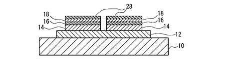
- a metal-ceramics bonded substrate shown in FIG. 4A to which the metal plate 18 is directly bonded is manufactured. After that, the aluminum or aluminum alloy in the portion corresponding to the molten metal flow path (runner) is removed, the surface of the second metal plate 18 is buffed, and the substantially entire surface of the surface is etched as shown in FIG. 4B.
- the etching resist 28, the second metal plate 18, the graphite sheet 16 and the first metal plate 14 are formed in the thickness direction from the surface of the etching resist 28. Is removed by milling, and a part of the first metal plate 14 on the ceramic substrate 12 side (to prevent the cutting tool from coming into contact with the ceramic substrate 12 and cracking the ceramic substrate 12 during milling). It is formed into a circuit pattern shape as shown in FIG. 4C, except that (a thin portion having a thickness of about 0.2 mm) is left. Then, as shown in FIG.
- the first metal plate 14 other than the portion corresponding to the circuit pattern shape on the surface of the ceramic substrate 12 is etched and removed with an etching solution such as an aqueous solution of iron chloride, and then the etching resist 28 is applied. It can be removed to produce a metal-ceramic bonded substrate with a circuit pattern (consisting of a first metal plate 14, a graphite sheet 16 and a second metal plate 18) as shown in FIG. ..
- the portion of the metal-ceramics bonded substrate thus produced such as a semiconductor element on the second metal plate 18, that requires soldering may be plated by Ni plating or the like.
- the mold 20 is moved into a joining furnace (not shown), and the inside of the joining furnace is made into a nitrogen atmosphere to reduce the oxygen concentration to 100 ppm or less, preferably 10 ppm or less. It is preferable to heat the mold 20 to the pouring temperature by temperature control, then heat the molten metal to the pouring temperature, pressurize the molten metal pre-measured with nitrogen gas at a predetermined pressure, and pour it into the mold 20 from the pouring port. ..
- the predetermined pressure pressurized by nitrogen gas during pouring and cooling is preferably 1 to 100 kPa, more preferably 3 to 80 kPa, and most preferably 5 to 15 kPa. If this pressure is too low, it becomes difficult for the molten metal to enter the mold 20, and if it is too high, the position of the graphite sheet 16 may shift or the mold 20 may break. In particular, when a carbon mold 20 is used, if the pressure is 1 MPa or more, the mold 20 may be destroyed or the molten metal may leak from the mold 20.
- FIG. 3 shows a mold 120 used to manufacture a modified example of the embodiment of the metal-ceramic bonded substrate according to the present invention.
- a recess (radiation fin forming portion) 126b for forming a heat radiation fin is formed on the bottom surface of the recess (metal base plate forming portion) 126a formed on the lower surface (back surface) of the upper mold member 126. Therefore, the heat radiation fins can be integrally formed on the bottom surface of the metal base plate. Since the other configurations are substantially the same as those of the mold 20 of FIG. 2, 100 is added to the reference numerals in FIG. 3 to omit the description thereof.
- the ceramic substrate may be an oxide-based ceramic substrate such as alumina, or a non-oxide ceramic substrate such as aluminum nitride or silicon nitride.
- Example 1 A ceramic substrate made of aluminum nitride (AlN) having a size of 50 mm ⁇ 50 mm ⁇ 0.6 mm (SH-30 manufactured by TD Power Material Co., Ltd.) in a carbon mold having the same shape as the mold 20 shown in FIG. And the size of 48 mm x 48 mm x 0.05 mm (the thermal conductivity in the horizontal direction is 1000 W / m ⁇ K, the thermal conductivity in the thickness direction is 20 W / m ⁇ K, and the linear expansion coefficient is 5 ppm / K).
- AlN aluminum nitride
- the mold After arranging a graphite sheet (PGS manufactured by Panasonic Corporation), the mold is placed in a furnace with a nitrogen atmosphere, and aluminum with a purity of 99.9% by mass (3N) (heat conductivity is 220 to 230 W / m. K, 0.2% aluminum with a resistance of 18 to 22 MPa) is poured into the mold, and then the molten metal is cooled and solidified (solidified) to form 70 mm x 70 mm x 5 mm on one surface of the ceramic substrate.
- the aluminum base plate of the size of is directly bonded, and one surface of the first aluminum plate for the circuit pattern of the size of 46 mm ⁇ 46 mm ⁇ 0.35 mm is directly bonded to the other surface of the ceramics substrate.
- One surface of the graphite sheet is directly bonded to the other surface of the aluminum plate of 1, and a second aluminum plate for a circuit pattern having a size of 46 mm ⁇ 46 mm ⁇ 0.2 mm is directly bonded to the other surface of the graphite sheet.
- a bonded metal-ceramics bonded substrate (the total thickness of the first aluminum plate, the graphite sheet, and the second aluminum plate was 0.6 mm) was obtained.
- the aluminum in the part corresponding to the molten metal flow path (runner) is removed, the surface of the second aluminum plate is buffed, an etching resist is formed on the surface, and then from the surface of the etching resist with a ⁇ 2 mm end mill.
- the etching resist, the second aluminum plate, the graphite sheet, and the first aluminum plate are removed by milling in the thickness direction from the ceramic substrate side of the first aluminum plate. It was formed in a circuit pattern shape except that a portion having a thickness of up to 0.2 mm was left. Then, the first aluminum plate other than the portion corresponding to the circuit pattern shape on the surface of the ceramic substrate was removed by etching with an aqueous solution of iron chloride, and then the etching resist was removed to obtain a size of 45 mm ⁇ 45 mm ⁇ 0.6 mm (No. 1). A metal-ceramics bonded substrate having a circuit pattern (composed of 1 aluminum plate, 1 graphite sheet, and 2nd aluminum plate) was obtained.
- Example 2 A metal-ceramic bonded substrate was produced by the same method as in Example 1 except that the thickness of the ceramic substrate was 0.3 mm, and the surface roughness Ra of the surface of the second aluminum plate and the grain boundaries of aluminum were used.
- the initial surface roughness Ra was 1.2 ⁇ m on average
- the initial grain boundary step was 10 ⁇ m or less on average
- the surface roughness Ra after heat cycle was 1.5 ⁇ m on average.
- the step at the grain boundary after the cycle was 30 ⁇ m or less at maximum.
- Example 3 A metal-ceramic bonded substrate was produced by the same method as in Example 1 except that a ceramic substrate made of silicon nitride having a thickness of 0.3 mm was used as the ceramic substrate, and the surface roughness of the surface of the second aluminum plate was roughened.
- the initial surface roughness Ra was 1.3 ⁇ m on average, and the step at the initial grain boundary was 10 ⁇ m or less at the maximum, and the surface roughness Ra after the heat cycle was measured.
- the average step was 1.5 ⁇ m, and the step at the grain boundary after the heat cycle was 30 ⁇ m or less at the maximum.
- Example 4 The metal was formed by the same method as in Example 1 except that the thickness of the graphite sheet was 0.1 mm, the thickness of the first aluminum plate was 0.9 mm, and the thickness of the second aluminum plate was 0.2 mm.
- -A ceramic bonded substrate was prepared, and the surface roughness Ra on the surface of the second aluminum plate and the step generated at the grain boundaries of aluminum were measured.
- the initial surface roughness Ra was 1.2 ⁇ m on average, and the initial crystal.
- the maximum step of the grain boundary was 10 ⁇ m or less, the surface roughness Ra after the heat cycle was 1.4 ⁇ m on average, and the step of the crystal grain boundary after the heat cycle was 20 ⁇ m or less at the maximum.
- Example 5 The metal was formed by the same method as in Example 2 except that the thickness of the graphite sheet was 0.1 mm, the thickness of the first aluminum plate was 0.9 mm, and the thickness of the second aluminum plate was 0.2 mm.
- -A ceramic bonded substrate was prepared, and the surface roughness Ra on the surface of the second aluminum plate and the step generated at the grain boundaries of aluminum were measured.
- the initial surface roughness Ra was 1.2 ⁇ m on average, and the initial crystal.
- the maximum step of the grain boundary was 10 ⁇ m or less, the surface roughness Ra after the heat cycle was 1.4 ⁇ m on average, and the step of the crystal grain boundary after the heat cycle was 20 ⁇ m or less at the maximum.
- Example 6 The metal was formed by the same method as in Example 3 except that the thickness of the graphite sheet was 0.1 mm, the thickness of the first aluminum plate was 0.9 mm, and the thickness of the second aluminum plate was 0.2 mm.
- -A ceramic bonded substrate was prepared, and the surface roughness Ra of the surface of the second aluminum plate and the step generated at the grain boundary of aluminum were measured.
- the initial surface roughness Ra was 1.3 ⁇ m on average, and the initial crystal.
- the maximum step of the grain boundary was 10 ⁇ m or less, the surface roughness Ra after the heat cycle was 1.4 ⁇ m on average, and the step of the crystal grain boundary after the heat cycle was 20 ⁇ m or less at the maximum.
- Example 1 A metal-ceramic bonded substrate was produced by the same method as in Example 1 except that the thickness of the aluminum plate was set to 0.6 mm without using the graphite sheet, and the surface roughness Ra and aluminum on the surface of the aluminum plate were prepared.
- the step generated at the grain boundary was measured, the initial surface roughness Ra was 1.2 ⁇ m on average, the step at the initial grain boundary was 10 ⁇ m or less on average, and the surface roughness Ra after the heat cycle was 1 on average.
- the maximum step of the grain boundary after the heat cycle was 9.9 ⁇ m, which was about 50 ⁇ m.
- a metal-ceramic bonded substrate was prepared by the same method as in Example 3 except that the thickness of the aluminum plate was set to 0.6 mm without using the graphite sheet, and the surface roughness Ra and aluminum on the surface of the aluminum plate were prepared.
- the steps generated at the grain boundaries of No. 1 were measured, the initial surface roughness Ra was 1.3 ⁇ m on average, the steps at the initial grain boundaries were up to 10 ⁇ m or less, and the surface roughness Ra after the heat cycle was 2 on average.
- the maximum step of the grain boundary after the heat cycle was about 50 ⁇ m.
- a metal-ceramic bonded substrate was prepared by the same method as in Example 1 except that the thickness of the aluminum plate was 1.2 mm without using the graphite sheet, and the surface roughness Ra and aluminum on the surface of the aluminum plate were prepared.
- the initial surface roughness Ra was 1.2 ⁇ m on average
- the steps at the initial grain boundaries were 10 ⁇ m or less on average
- the surface roughness Ra after the heat cycle was 2 on average.
- the step of the grain boundary after the heat cycle was about 80 ⁇ m at the maximum.
- a metal-ceramic bonded substrate was prepared by the same method as in Example 3 except that the thickness of the aluminum plate was 1.2 mm without using the graphite sheet, and the surface roughness Ra and aluminum on the surface of the aluminum plate were prepared.
- the steps generated at the grain boundaries of No. 1 were measured, the initial surface roughness Ra was 1.3 ⁇ m on average, the steps at the initial grain boundaries were up to 10 ⁇ m or less, and the surface roughness Ra after the heat cycle was 2 on average.
- the maximum step at the grain boundary after the heat cycle was about 80 ⁇ m.
- Example 7 instead of molten aluminum, an aluminum alloy containing 0.4% by mass of silicon and 0.05% by mass of boron (thermal conductivity of 180 to 200 W / m ⁇ K, 0.2% strength of 20 to 23 MPa)
- a metal-ceramics bonded substrate was produced by the same method as in Example 4 except that the molten metal of (aluminum alloy) was used, and the surface roughness Ra on the surface of the second aluminum plate and the crystal grain boundary of aluminum were generated.
- the initial surface roughness Ra was 1.3 ⁇ m on average
- the step at the initial crystal grain boundary was 10 ⁇ m or less at the maximum
- the surface roughness Ra after the heat cycle was 1.4 ⁇ m on average, after the heat cycle.
- the maximum step at the crystal grain boundary was 20 ⁇ m or less.
- Example 8 instead of molten aluminum, an aluminum alloy containing 0.4% by mass of silicon and 0.05% by mass of boron (thermal conductivity of 180 to 200 W / m ⁇ K, 0.2% strength of 20 to 23 MPa)
- a metal-ceramics bonded substrate was produced by the same method as in Example 6 except that the molten metal of (aluminum alloy) was used, and the surface roughness Ra on the surface of the second aluminum plate and the crystal grain boundary of aluminum were generated.
- the initial surface roughness Ra was 1.4 ⁇ m on average
- the step at the initial crystal grain boundary was 10 ⁇ m or less at maximum
- the surface roughness Ra after heat cycle was 1.5 ⁇ m on average, after the heat cycle.
- the maximum step at the crystal grain boundary was 20 ⁇ m or less.
- Example 9 instead of molten aluminum, an aluminum alloy containing 0.05% by mass of magnesium and 0.04% by mass of silicon (thermal conductivity of 190 to 210 W / m ⁇ K, 0.2% resistance of 20 to 23 MPa)
- a metal-ceramics bonded substrate was produced by the same method as in Example 4 except that the molten metal of (aluminum alloy) was used, and the surface roughness Ra on the surface of the second aluminum plate and the crystal grain boundary of aluminum were generated.
- the step was measured, the initial surface roughness Ra was 1.2 ⁇ m on average, the step at the initial crystal grain boundary was 10 ⁇ m or less at maximum, and the surface roughness Ra after heat cycle was 1.4 ⁇ m on average, after the heat cycle.
- the maximum step at the crystal grain boundary was 20 ⁇ m or less.
- Example 10 instead of molten aluminum, an aluminum alloy containing 0.05% by mass of magnesium and 0.04% by mass of silicon (thermal conductivity of 190 to 210 W / m ⁇ K, 0.2% resistance of 20 to 23 MPa)
- a metal-ceramics bonded substrate was produced by the same method as in Example 6 except that the molten metal of (aluminum alloy) was used, and the surface roughness Ra on the surface of the second aluminum plate and the crystal grain boundary of aluminum were generated.
- the initial surface roughness Ra was 1.3 ⁇ m on average
- the step at the initial crystal grain boundary was 10 ⁇ m or less at the maximum
- the surface roughness Ra after the heat cycle was 1.4 ⁇ m on average, after the heat cycle.
- the maximum step at the crystal grain boundary was 20 ⁇ m or less.
- Example 11 instead of molten aluminum, an aluminum alloy containing 0.08% by mass of magnesium and 0.06% by mass of silicon (thermal conductivity of 180 to 200 W / mK, 0.2% strength of 25 to 30 MPa)
- a metal-ceramics bonded substrate was produced by the same method as in Example 4 except that the molten metal of (aluminum alloy) was used, and the surface roughness Ra on the surface of the second aluminum plate and the crystal grain boundary of aluminum were generated.
- the initial surface roughness Ra was 1.2 ⁇ m on average
- the step at the initial crystal grain boundary was 10 ⁇ m or less at maximum
- the surface roughness Ra after heat cycle was 1.4 ⁇ m on average, after the heat cycle.
- the maximum step at the crystal grain boundary was 10 ⁇ m or less.
- Example 12 instead of molten aluminum, an aluminum alloy containing 0.08% by mass of magnesium and 0.06% by mass of silicon (thermal conductivity of 180 to 200 W / mK, 0.2% strength of 25 to 30 MPa)
- a metal-ceramics bonded substrate was produced by the same method as in Example 6 except that the molten metal of (aluminum alloy) was used, and the surface roughness Ra on the surface of the second aluminum plate and the crystal grain boundary of aluminum were generated.
- the initial surface roughness Ra was 1.3 ⁇ m on average
- the step at the initial crystal grain boundary was 10 ⁇ m or less at the maximum
- the surface roughness Ra after the heat cycle was 1.4 ⁇ m on average, after the heat cycle.
- the maximum step at the crystal grain boundary was 10 ⁇ m or less.
- Example 13 instead of the molten aluminum, a molten aluminum alloy containing 0.1% by mass of zirconium (aluminum alloy having a thermal conductivity of 180 to 200 W / m ⁇ K and a 0.2% resistance of 25 to 30 MPa) was used.
- a metal-ceramics bonded substrate was produced by the same method as in Example 4 except for the above, and the surface roughness Ra of the surface of the second aluminum plate and the step generated at the grain boundary of aluminum were measured.
- the surface roughness Ra has an average of 1.2 ⁇ m and the initial grain boundary step is 10 ⁇ m or less, the surface roughness Ra after the heat cycle has an average of 1.5 ⁇ m, and the grain boundary step after the heat cycle has a maximum of 10 ⁇ m. It was as follows.
- Example 14 instead of the molten aluminum, a molten aluminum alloy containing 0.1% by mass of zirconium (aluminum alloy having a thermal conductivity of 180 to 200 W / m ⁇ K and a 0.2% resistance of 25 to 30 MPa) was used.
- a metal-ceramics bonded substrate was prepared by the same method as in Example 6 except for the above, and the surface roughness Ra of the surface of the second aluminum plate and the step generated at the grain boundary of aluminum were measured.
- the average surface roughness Ra is 1.3 ⁇ m
- the initial grain boundary step is 10 ⁇ m or less
- the surface roughness Ra after the heat cycle is 1.5 ⁇ m on average
- the grain boundary step after the heat cycle is 10 ⁇ m at maximum. It was as follows.
- Example 15 instead of the molten aluminum, a molten aluminum alloy containing 0.2% by mass of zirconium (aluminum alloy having a thermal conductivity of 170 to 190 W / m ⁇ K and a 0.2% resistance of 27 to 32 MPa) was used. Except for this, a metal-ceramics bonded substrate was produced by the same method as in Example 4, and the surface roughness Ra of the surface of the second aluminum plate and the step generated at the grain boundary of aluminum were measured. The average surface roughness Ra is 1.2 ⁇ m, the initial step of the grain boundary is 10 ⁇ m or less, the average surface roughness Ra after the heat cycle is 1.4 ⁇ m, and the maximum step of the grain boundary after the heat cycle is 10 ⁇ m. It was as follows.
- Example 16 instead of the molten aluminum, a molten aluminum alloy containing 0.2% by mass of zirconium (aluminum alloy having a thermal conductivity of 170 to 190 W / m ⁇ K and a 0.2% resistance of 27 to 32 MPa) was used.
- a metal-ceramics bonded substrate was prepared by the same method as in Example 6 except for the above, and the surface roughness Ra of the surface of the second aluminum plate and the step generated at the grain boundary of aluminum were measured.
- the average surface roughness Ra is 1.3 ⁇ m
- the initial grain boundary step is 10 ⁇ m or less
- the surface roughness Ra after the heat cycle is 1.4 ⁇ m on average
- the grain boundary step after the heat cycle is 10 ⁇ m at maximum. It was as follows.
- Example 17 instead of the molten aluminum, a molten aluminum alloy containing 0.1% by mass of zinc (aluminum alloy having a thermal conductivity of 180 to 200 W / m ⁇ K and a 0.2% resistance of 25 to 30 MPa) was used. Except for this, a metal-ceramics bonded substrate was produced by the same method as in Example 4, and the surface roughness Ra of the surface of the second aluminum plate and the step generated at the grain boundary of aluminum were measured.
- the average surface roughness Ra is 1.3 ⁇ m
- the initial grain boundary step is 10 ⁇ m or less
- the surface roughness Ra after the heat cycle is 1.5 ⁇ m on average
- the grain boundary step after the heat cycle is 10 ⁇ m at maximum. It was as follows.
- Example 18 instead of the molten aluminum, a molten aluminum alloy containing 0.1% by mass of zinc (aluminum alloy having a thermal conductivity of 180 to 200 W / m ⁇ K and a 0.2% resistance of 25 to 30 MPa) was used.
- a metal-ceramics bonded substrate was prepared by the same method as in Example 6 except for the above, and the surface roughness Ra of the surface of the second aluminum plate and the step generated at the grain boundary of aluminum were measured.
- the average surface roughness Ra is 1.3 ⁇ m
- the initial grain boundary step is 10 ⁇ m or less
- the surface roughness Ra after the heat cycle is 1.5 ⁇ m on average
- the grain boundary step after the heat cycle is 10 ⁇ m at maximum. It was as follows.
- Example 19 instead of the molten aluminum, a molten aluminum alloy containing 0.2% by mass of zinc (aluminum alloy having a thermal conductivity of 170 to 190 W / m ⁇ K and a 0.2% resistance of 27 to 32 MPa) was used. Except for this, a metal-ceramics bonded substrate was produced by the same method as in Example 4, and the surface roughness Ra of the surface of the second aluminum plate and the step generated at the grain boundary of aluminum were measured. The average surface roughness Ra is 1.3 ⁇ m, the initial grain boundary step is 10 ⁇ m or less, the surface roughness Ra after the heat cycle is 1.4 ⁇ m on average, and the grain boundary step after the heat cycle is 10 ⁇ m at maximum. It was as follows.
- Example 20 instead of the molten aluminum, a molten aluminum alloy containing 0.2% by mass of zinc (aluminum alloy having a thermal conductivity of 170 to 190 W / m ⁇ K and a 0.2% resistance of 27 to 32 MPa) was used.
- a metal-ceramics bonded substrate was prepared by the same method as in Example 6 except for the above, and the surface roughness Ra of the surface of the second aluminum plate and the step generated at the grain boundary of aluminum were measured.
- the average surface roughness Ra is 1.3 ⁇ m
- the initial grain boundary step is 10 ⁇ m or less
- the surface roughness Ra after the heat cycle is 1.4 ⁇ m on average
- the grain boundary step after the heat cycle is 10 ⁇ m at maximum. It was as follows.
- Example 5 A metal-ceramics bonded substrate was prepared by the same method as in Example 7 except that a graphite sheet was not used, and the surface roughness Ra of the surface of the aluminum plate and the step generated at the grain boundary of aluminum were measured.
- the initial surface roughness Ra is 1.3 ⁇ m on average
- the step of the initial grain boundary is 10 ⁇ m or less at the maximum
- the surface roughness Ra after the heat cycle is 1.7 ⁇ m on average, which is the grain boundary after the heat cycle.
- the maximum step was about 50 ⁇ m.
- a metal-ceramics bonded substrate was prepared by the same method as in Example 8 except that the graphite sheet was not used, and the surface roughness Ra of the surface of the aluminum plate and the step generated at the grain boundary of aluminum were measured.
- the initial surface roughness Ra is 1.4 ⁇ m on average
- the step of the initial grain boundary is 10 ⁇ m or less at the maximum
- the surface roughness Ra after the heat cycle is 1.8 ⁇ m on average, which is the grain boundary after the heat cycle.
- the maximum step was about 50 ⁇ m.
- Example 7 A metal-ceramics bonded substrate was prepared by the same method as in Example 11 except that the graphite sheet was not used, and the surface roughness Ra of the surface of the aluminum plate and the step generated at the grain boundary of aluminum were measured.
- the initial surface roughness Ra is 1.2 ⁇ m on average
- the step of the initial grain boundary is 10 ⁇ m or less at the maximum
- the surface roughness Ra after the heat cycle is 1.7 ⁇ m on average, which is the grain boundary after the heat cycle.
- the maximum step was about 50 ⁇ m.
- Example 8 A metal-ceramics bonded substrate was prepared by the same method as in Example 12 except that the graphite sheet was not used, and the surface roughness Ra of the surface of the aluminum plate and the step generated at the grain boundary of aluminum were measured.
- the initial surface roughness Ra is 1.3 ⁇ m on average
- the step of the initial grain boundary is 10 ⁇ m or less at the maximum
- the surface roughness Ra after the heat cycle is 1.7 ⁇ m on average, which is the grain boundary after the heat cycle.
- the maximum step was about 50 ⁇ m.
- the level difference of the crystal grain boundaries after heat-sixing has a relatively large variation depending on the solid, but it can be suppressed to a maximum of 30 ⁇ m or less in the examples, whereas it is as large as about 50 ⁇ m to about 80 ⁇ m in the comparative example. , It turns out that it is not suitable for manufacturing a metal-ceramic bonded substrate as a mass-produced product. Further, in the embodiment, a metal-ceramic bonding substrate in which a thick aluminum plate in which the total thickness of the first aluminum plate and the second aluminum plate is 0.5 mm or more (further 0.8 mm or more) is bonded to the ceramic substrate.
- a substrate can be provided.
- Metal base plate 12 Ceramic substrate 14 First metal plate 16 Graphite sheet 18 Second metal plate 20, 120 Molds 22, 122 Lower mold members 22a, 122a Graphite sheet accommodating parts 22b, 122b Second metal plate forming parts 24, 124 Intermediate mold members 24a, 124a Metal base plate forming parts 24b, 124b Ceramic substrate housing parts 24c, 124c First metal plate forming parts 24d, 124d Graphite sheet housing parts 26, 126 Upper mold members 26a, 126a Metal base plate Forming part 126b Heat dissipation fin forming part
Landscapes
- Engineering & Computer Science (AREA)
- Microelectronics & Electronic Packaging (AREA)
- Ceramic Products (AREA)
- Chemical & Material Sciences (AREA)
- Ceramic Engineering (AREA)
- Cooling Or The Like Of Semiconductors Or Solid State Devices (AREA)
Abstract
La présente invention concerne : un substrat composite métal-céramique assemblé à moindre coût comprenant un substrat céramique et une carte de circuit métallique constituée d'aluminium ou d'un alliage d'aluminium et directement assemblée avec le substrat céramique ; et son procédé de fabrication. La présente invention empêche une différence de niveau importante de se produire à un emplacement correspondant au joint de grain cristallin de l'aluminium ou de l'alliage d'aluminium même si un cycle thermique est appliqué de manière répétée. Dans un mode de réalisation du substrat métal-céramique assemblé : une surface d'un substrat céramique (12) s'assemble directement avec une plaque de base métallique (10) en aluminium ou en alliage d'aluminium ; une surface d'une première plaque métallique (14) pour un motif de circuit, qui est constituée d'aluminium ou d'un alliage d'aluminium, s'assemble directement avec l'autre surface du substrat céramique ; une surface de feuille de graphène (16) s'assemble directement avec l'autre surface de la première plaque métallique ; et une seconde plaque métallique (18) pour un motif de circuit, qui est constituée d'aluminium ou d'un alliage d'aluminium, s'assemble directement avec l'autre surface de la feuille de graphène.
Priority Applications (2)
| Application Number | Priority Date | Filing Date | Title |
|---|---|---|---|
| US17/623,293 US12300512B2 (en) | 2019-06-28 | 2020-06-11 | Metal/ceramic bonding substrate and method for producing same |
| EP20832352.7A EP3968366A4 (fr) | 2019-06-28 | 2020-06-11 | Substrat métal-céramique assemblé et son procédé de fabrication |
Applications Claiming Priority (4)
| Application Number | Priority Date | Filing Date | Title |
|---|---|---|---|
| JP2019122001 | 2019-06-28 | ||
| JP2019-122001 | 2019-06-28 | ||
| JP2020-092939 | 2020-05-28 | ||
| JP2020092939A JP7422608B2 (ja) | 2019-06-28 | 2020-05-28 | 金属-セラミックス接合基板およびその製造方法 |
Publications (1)
| Publication Number | Publication Date |
|---|---|
| WO2020262015A1 true WO2020262015A1 (fr) | 2020-12-30 |
Family
ID=74061909
Family Applications (1)
| Application Number | Title | Priority Date | Filing Date |
|---|---|---|---|
| PCT/JP2020/022998 Ceased WO2020262015A1 (fr) | 2019-06-28 | 2020-06-11 | Substrat métal-céramique assemblé et son procédé de fabrication |
Country Status (3)
| Country | Link |
|---|---|
| US (1) | US12300512B2 (fr) |
| EP (1) | EP3968366A4 (fr) |
| WO (1) | WO2020262015A1 (fr) |
Cited By (1)
| Publication number | Priority date | Publication date | Assignee | Title |
|---|---|---|---|---|
| WO2025203607A1 (fr) * | 2024-03-29 | 2025-10-02 | 株式会社Uacj | Matériau de coulée en alliage d'aluminium et procédé de production d'un matériau de coulée en alliage d'aluminium |
Families Citing this family (1)
| Publication number | Priority date | Publication date | Assignee | Title |
|---|---|---|---|---|
| TWI768966B (zh) * | 2021-06-15 | 2022-06-21 | 許國誠 | 石墨複合層疊散熱結構及其製造方法 |
Citations (8)
| Publication number | Priority date | Publication date | Assignee | Title |
|---|---|---|---|---|
| JP2007036263A (ja) | 2001-03-01 | 2007-02-08 | Dowa Holdings Co Ltd | 半導体実装用絶縁基板及びパワーモジュール |
| JP2008199057A (ja) * | 2006-06-02 | 2008-08-28 | Nec Lighting Ltd | 電子機器および電子機器の製造方法 |
| JP2015076445A (ja) * | 2013-10-07 | 2015-04-20 | 富士通株式会社 | 放熱器及びその製造方法 |
| JP2016152324A (ja) | 2015-02-18 | 2016-08-22 | Dowaメタルテック株式会社 | 金属−セラミックス回路基板の製造方法 |
| JP2017212316A (ja) * | 2016-05-25 | 2017-11-30 | Dowaホールディングス株式会社 | 金属−セラミックス接合基板およびその製造方法 |
| JP2018018992A (ja) | 2016-07-29 | 2018-02-01 | Dowaメタルテック株式会社 | 金属−セラミックス回路基板およびその製造方法 |
| JP2018135251A (ja) * | 2017-02-23 | 2018-08-30 | 三菱マテリアル株式会社 | パワーモジュール用基板の製造方法 |
| JP2019029510A (ja) * | 2017-07-31 | 2019-02-21 | Dowaメタルテック株式会社 | アルミニウム−セラミックス接合基板およびその製造方法 |
Family Cites Families (4)
| Publication number | Priority date | Publication date | Assignee | Title |
|---|---|---|---|---|
| CN102742008B (zh) | 2010-02-05 | 2015-07-01 | 三菱综合材料株式会社 | 功率模块用基板及功率模块 |
| WO2015087714A1 (fr) | 2013-12-09 | 2015-06-18 | 積水化学工業株式会社 | Produit d'étanchéité pour élément d'affichage |
| CN104754913B (zh) * | 2013-12-27 | 2018-06-05 | 华为技术有限公司 | 导热复合材料片及其制作方法 |
| TWI659828B (zh) * | 2016-07-27 | 2019-05-21 | 日商Jx金屬股份有限公司 | 附散熱用金屬材之結構物、印刷電路板、電子機器及散熱用金屬材 |
-
2020
- 2020-06-11 WO PCT/JP2020/022998 patent/WO2020262015A1/fr not_active Ceased
- 2020-06-11 EP EP20832352.7A patent/EP3968366A4/fr active Pending
- 2020-06-11 US US17/623,293 patent/US12300512B2/en active Active
Patent Citations (8)
| Publication number | Priority date | Publication date | Assignee | Title |
|---|---|---|---|---|
| JP2007036263A (ja) | 2001-03-01 | 2007-02-08 | Dowa Holdings Co Ltd | 半導体実装用絶縁基板及びパワーモジュール |
| JP2008199057A (ja) * | 2006-06-02 | 2008-08-28 | Nec Lighting Ltd | 電子機器および電子機器の製造方法 |
| JP2015076445A (ja) * | 2013-10-07 | 2015-04-20 | 富士通株式会社 | 放熱器及びその製造方法 |
| JP2016152324A (ja) | 2015-02-18 | 2016-08-22 | Dowaメタルテック株式会社 | 金属−セラミックス回路基板の製造方法 |
| JP2017212316A (ja) * | 2016-05-25 | 2017-11-30 | Dowaホールディングス株式会社 | 金属−セラミックス接合基板およびその製造方法 |
| JP2018018992A (ja) | 2016-07-29 | 2018-02-01 | Dowaメタルテック株式会社 | 金属−セラミックス回路基板およびその製造方法 |
| JP2018135251A (ja) * | 2017-02-23 | 2018-08-30 | 三菱マテリアル株式会社 | パワーモジュール用基板の製造方法 |
| JP2019029510A (ja) * | 2017-07-31 | 2019-02-21 | Dowaメタルテック株式会社 | アルミニウム−セラミックス接合基板およびその製造方法 |
Non-Patent Citations (1)
| Title |
|---|
| See also references of EP3968366A4 |
Cited By (1)
| Publication number | Priority date | Publication date | Assignee | Title |
|---|---|---|---|---|
| WO2025203607A1 (fr) * | 2024-03-29 | 2025-10-02 | 株式会社Uacj | Matériau de coulée en alliage d'aluminium et procédé de production d'un matériau de coulée en alliage d'aluminium |
Also Published As
| Publication number | Publication date |
|---|---|
| EP3968366A4 (fr) | 2023-07-12 |
| EP3968366A1 (fr) | 2022-03-16 |
| US12300512B2 (en) | 2025-05-13 |
| US20220367316A1 (en) | 2022-11-17 |
Similar Documents
| Publication | Publication Date | Title |
|---|---|---|
| JP4133170B2 (ja) | アルミニウム−セラミックス接合体 | |
| JP4543279B2 (ja) | アルミニウム接合部材の製造方法 | |
| JP4692708B2 (ja) | セラミックス回路基板およびパワーモジュール | |
| JP4965305B2 (ja) | 金属−セラミックス接合基板の製造方法 | |
| CN102574361A (zh) | 层合材料及其制造方法 | |
| JP5619437B2 (ja) | 金属−セラミックス接合基板の製造方法 | |
| JPWO2018131583A1 (ja) | 金属−セラミックス接合基板及びその製造方法 | |
| WO2012127695A1 (fr) | Substrat lié métal-céramique et procédé pour sa fabrication | |
| WO2020262015A1 (fr) | Substrat métal-céramique assemblé et son procédé de fabrication | |
| JP2004207587A (ja) | 金属−セラミックス接合基板およびその製造方法 | |
| JP6020256B2 (ja) | ヒートシンク付パワーモジュール用基板の製造方法 | |
| JP7062464B2 (ja) | アルミニウム-セラミックス接合基板およびその製造方法 | |
| JP4565249B2 (ja) | 金属−セラミックス接合基板およびその製造方法 | |
| JP4806803B2 (ja) | 金属−セラミックス接合基板およびその製造方法 | |
| JP5467407B2 (ja) | アルミニウム−セラミックス接合体 | |
| JP7422608B2 (ja) | 金属-セラミックス接合基板およびその製造方法 | |
| JPH10190176A (ja) | 回路基板 | |
| JP4821013B2 (ja) | アルミニウム−セラミックス接合基板およびその製造方法 | |
| JP2017139508A (ja) | パワーモジュール用基板製造のための接合体 | |
| JP5380734B2 (ja) | アルミニウム接合部材 | |
| JP3837680B2 (ja) | 金属−セラミックス複合基板製造用鋳型 | |
| JP2016048789A (ja) | アルミニウム−セラミックス接合体の製造方法 | |
| JP3871599B2 (ja) | 構造物 | |
| JP2022157227A (ja) | 金属-セラミックス接合基板およびその製造方法 | |
| JP2010267997A (ja) | セラミックス回路基板およびパワーモジュール |
Legal Events
| Date | Code | Title | Description |
|---|---|---|---|
| 121 | Ep: the epo has been informed by wipo that ep was designated in this application |
Ref document number: 20832352 Country of ref document: EP Kind code of ref document: A1 |
|
| ENP | Entry into the national phase |
Ref document number: 2020832352 Country of ref document: EP Effective date: 20211208 |
|
| NENP | Non-entry into the national phase |
Ref country code: DE |
|
| WWG | Wipo information: grant in national office |
Ref document number: 17623293 Country of ref document: US |