EP3968366A1 - Substrat métal-céramique assemblé et son procédé de fabrication - Google Patents
Substrat métal-céramique assemblé et son procédé de fabrication Download PDFInfo
- Publication number
- EP3968366A1 EP3968366A1 EP20832352.7A EP20832352A EP3968366A1 EP 3968366 A1 EP3968366 A1 EP 3968366A1 EP 20832352 A EP20832352 A EP 20832352A EP 3968366 A1 EP3968366 A1 EP 3968366A1
- Authority
- EP
- European Patent Office
- Prior art keywords
- metal
- aluminum
- graphite sheet
- ceramic
- plate
- Prior art date
- Legal status (The legal status is an assumption and is not a legal conclusion. Google has not performed a legal analysis and makes no representation as to the accuracy of the status listed.)
- Pending
Links
Images
Classifications
-
- H—ELECTRICITY
- H05—ELECTRIC TECHNIQUES NOT OTHERWISE PROVIDED FOR
- H05K—PRINTED CIRCUITS; CASINGS OR CONSTRUCTIONAL DETAILS OF ELECTRIC APPARATUS; MANUFACTURE OF ASSEMBLAGES OF ELECTRICAL COMPONENTS
- H05K1/00—Printed circuits
- H05K1/02—Details
- H05K1/0201—Thermal arrangements, e.g. for cooling, heating or preventing overheating
- H05K1/0203—Cooling of mounted components
-
- H—ELECTRICITY
- H10—SEMICONDUCTOR DEVICES; ELECTRIC SOLID-STATE DEVICES NOT OTHERWISE PROVIDED FOR
- H10W—GENERIC PACKAGES, INTERCONNECTIONS, CONNECTORS OR OTHER CONSTRUCTIONAL DETAILS OF DEVICES COVERED BY CLASS H10
- H10W40/00—Arrangements for thermal protection or thermal control
- H10W40/20—Arrangements for cooling
- H10W40/25—Arrangements for cooling characterised by their materials
- H10W40/255—Arrangements for cooling characterised by their materials having a laminate or multilayered structure, e.g. direct bond copper [DBC] ceramic substrates
-
- H—ELECTRICITY
- H10—SEMICONDUCTOR DEVICES; ELECTRIC SOLID-STATE DEVICES NOT OTHERWISE PROVIDED FOR
- H10W—GENERIC PACKAGES, INTERCONNECTIONS, CONNECTORS OR OTHER CONSTRUCTIONAL DETAILS OF DEVICES COVERED BY CLASS H10
- H10W70/00—Package substrates; Interposers; Redistribution layers [RDL]
- H10W70/01—Manufacture or treatment
- H10W70/02—Manufacture or treatment of conductive package substrates serving as an interconnection, e.g. of metal plates
-
- H—ELECTRICITY
- H10—SEMICONDUCTOR DEVICES; ELECTRIC SOLID-STATE DEVICES NOT OTHERWISE PROVIDED FOR
- H10W—GENERIC PACKAGES, INTERCONNECTIONS, CONNECTORS OR OTHER CONSTRUCTIONAL DETAILS OF DEVICES COVERED BY CLASS H10
- H10W99/00—Subject matter not provided for in other groups of this subclass
-
- H—ELECTRICITY
- H10—SEMICONDUCTOR DEVICES; ELECTRIC SOLID-STATE DEVICES NOT OTHERWISE PROVIDED FOR
- H10W—GENERIC PACKAGES, INTERCONNECTIONS, CONNECTORS OR OTHER CONSTRUCTIONAL DETAILS OF DEVICES COVERED BY CLASS H10
- H10W40/00—Arrangements for thermal protection or thermal control
- H10W40/20—Arrangements for cooling
- H10W40/25—Arrangements for cooling characterised by their materials
Definitions
- the present invention generally relates to a metal/ceramic bonding substrate and a method for producing the same. More specifically, the invention relates to a metal/ceramic bonding substrate wherein a metal plate (a metal circuit plate) for mounting electronic parts thereon is formed on one side of a ceramic substrate and wherein a metal base plate for heat radiation is formed on the other side thereof, and a method for producing the same.
- a metal plate a metal circuit plate for mounting electronic parts thereon
- a metal/ceramic insulating substrate for a power module there is used a metal/ceramic circuit board wherein a metal circuit plate of aluminum or an aluminum alloy is bonded directly to a ceramic substrate in order to realize a higher heat cycle resistance.
- a semiconductor packing insulating substrate wherein a metal alloy layer (mainly containing aluminum) having a Vickers hardness HV of not less than 25 is formed on a ceramic substrate (see, e.g., Patent Document 1), a metal/ceramic circuit board wherein a metal film of copper, a copper alloy or the like is formed, by a cold spraying method, on a metal circuit plate of aluminum or an aluminum alloy which is formed on a ceramic substrate (see, e.g., Patent Document 2), a metal/ceramic circuit board wherein a nickel-plating film having a thickness of not less than 17 ⁇ m is formed on the surface of a metal circuit plate of aluminum bonded directly to a ceramic substrate (see, e.g., Patent Document 3) and so forth.
- Patent Document 1 a metal alloy layer (mainly containing aluminum) having a Vickers hardness HV of not less than 25 is formed on a ceramic substrate
- Patent Document 2 a metal/ceramic circuit board wherein a metal film of copper,
- the hard metal film formed by the cold spraying method is porous, and the surface thereof is rough. For that reason, it is required to cause the surface of the metal film to be smooth by blasting or the like, so that the producing costs thereof are increased.
- the inventors have diligently studied and found that it is possible to produce an inexpensive metal/ceramic bonding substrate which can prevent a large difference in level from being caused on portions corresponding to the grain boundaries of aluminum or an aluminum alloy even if heat cycles are repeatedly applied to the metal/ceramic bonding substrate, if one side of a ceramic substrate is bonded directly to a metal base plate of aluminum or an aluminum alloy, one side of a first metal plate of aluminum or the aluminum alloy being bonded directly to the other side of the ceramic substrate, one side of a graphite sheet being bonded directly to the other side of the first metal plate, and a second metal plate of aluminum or the aluminum alloy being bonded directly to the other side of the graphite sheet.
- the inventors have made the present invention.
- a metal/ceramic bonding substrate comprising: a metal base plate of aluminum or an aluminum alloy; a ceramic substrate, one side of which is bonded directly to the metal base plate; a first metal plate of aluminum or the aluminum alloy, one side of which is bonded directly to the other side of the ceramic substrate; a graphite sheet, one side of which is bonded directly to the other side of the first metal plate; and a second metal plate of aluminum or the aluminum alloy which is bonded directly to the other side of the graphite sheet.
- the graphite sheet preferably extends in substantially parallel to a bonding surface of the first metal plate to the ceramic substrate, and preferably extends on a substantially entire surface of a plane which extends in substantially parallel to the bonding surface of the first metal plate to the ceramic substrate.
- the graphite sheet preferably has an end face which is exposed to the outside.
- a circuit pattern is preferably formed by the first metal plate, the graphite sheet and the second metal plate.
- a method for producing a metal/ceramic bonding substrate comprising the steps of: causing a peripheral portion of a graphite sheet and a peripheral portion of a ceramic substrate to be supported on a mold so that the graphite sheet and the ceramic substrate are arranged in substantially parallel to each other in the mold so as to be apart from each other; injecting a molten metal of aluminum or an aluminum alloy into the mold so as to allow the molten metal to contact both sides of the graphite sheet and both sides of the ceramic substrate in the mold; and cooling and solidifying the molten metal in the mold to form a metal base plate of aluminum or the aluminum alloy to bond the metal base plate directly to one side of the ceramic substrate, while forming a first metal plate of aluminum or the aluminum alloy to bond the first metal plate directly to one side of the graphite sheet and to the other side of the ceramic substrate, and while forming a second metal plate of aluminum or the aluminum alloy to bond the second metal plate directly to the other side of the graphite sheet
- the method further comprises: forming a mask on the surface of the second metal plate of the metal/ceramic bonding substrate; removing a portion other than a portion, which corresponds to a shape of a circuit pattern of the mask, second metal plate, graphite sheet and first metal plate, in thickness directions thereof from the surface of the mask by milling to cause the mask, the second metal plate, the graphite sheet and the first metal plate to have the shape of the circuit pattern, except that a portion of the first metal plate on the side of the ceramic substrate is caused to remain; etching the portion of the first metal plate other than the portion, which corresponds to the shape of the circuit pattern, on the surface of the ceramic substrate; and removing the mask to form the circuit pattern of the first metal plate, graphite sheet and second metal plate.
- an inexpensive metal/ceramic bonding substrate which has a metal circuit plate of aluminum or an aluminum alloy bonded directly to a ceramic substrate and which can prevent a large difference in level from being caused on portions corresponding to the grain boundaries of aluminum or the aluminum alloy even if heat cycles are repeatedly applied to the metal/ceramic bonding substrate.
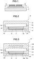
- the preferred embodiment of a metal/ceramic bonding substrate comprises: a metal base plate 10 of aluminum or an aluminum alloy having a substantially rectangular planar shape; a ceramic substrate 12 having a substantially rectangular planar shape, one side of the ceramic substrate being bonded directly to the metal base plate 10 (chemically bonded to the metal base plate 10 at a sufficient bonding strength); a first metal plate (for circuit pattern) 14 of aluminum or the aluminum alloy having a substantially rectangular planar shape, one side of the first metal plate 14 being bonded directly to the other side of the ceramic substrate 12 (chemically bonded to the other side of the ceramic substrate 12 at a sufficient bonding strength); a graphite sheet 16 having a substantially rectangular planar shape (substantially having the same size as that of the first metal plate 14), one side of the graphite sheet 16 being bonded directly to the other side of the first metal plate 14 (chemically bonded to the other side of the first metal plate 14 at a sufficient bonding strength); and a second metal plate (for
- the graphite sheet 16 extends in substantially parallel to the bonding surface of the first metal plate 14 to the ceramic substrate 12 and extends on the substantially entire surface of a plane (an imaginary plane) which extends in substantially parallel to the bonding surface of the first metal plate 14 to the ceramic substrate 12.
- the peripheral portion (preferably over the entire circumference) of the graphite sheet 16 is exposed to the outside.
- the graphite sheet 16 may be a sheet (plate material) of graphite having a thickness of 10 to 1000 ⁇ m (preferably 30 to 120 ⁇ m), a thermal conductivity of 250 to 2000 W/m ⁇ K (preferably 900 to 2000 W/m ⁇ K) in horizontal directions, a thermal conductivity of 10 to 30 W/m ⁇ K (preferably 18 to 30 W/m ⁇ K) in thickness directions and a linear expansion coefficient of 2 to 10 ppm/K (preferably 4 to 7 ppm/K).
- a graphite sheet 16 is arranged between the first metal plate (for circuit pattern) 14 and the second metal plate (for circuit pattern) 18, it is possible to produce a metal/ceramic bonding substrate which can suppress the distortion (deformation) of the surface of the second metal plate (for circuit pattern) 18 and which can inhibit winkles from being caused on the surface of the second metal plate (for circuit pattern) 18 after heat cycles, the metal/ceramic bonding substrate being capable of preventing heat cycles from producing cracks in the ceramic substrate 12 and semiconductor devices or the like (mounted on the second metal plate 18) to decrease the producing costs thereof, the metal/ceramic bonding substrate having excellent thermal conductivity and excellent electrical conductivity.
- the second metal plate 18 is arranged on the outermost surface, it is possible to carry out the plating of the surface, the ultrasonic bonding using an aluminum wire, a copper wire or the like, and the ultrasonic bonding of a copper terminal.
- the metal/ceramic bonding substrate in the preferred embodiment shown in FIG. 1 can be produced by a method comprising the steps of: causing the peripheral portion of a ceramic substrate 12 and the peripheral portion of a graphite sheet 16 to be supported on a mold 20 shown in FIG.
- the ceramic substrate 12 and the graphite sheet 16 are arranged so as to be spaced apart from each other in the mold 20; heating the interior of the mold 20 in a state that the atmosphere therein is an atmosphere of nitrogen; injecting a molten metal of aluminum or an aluminum alloy into the mold 20 so as to allow the molten metal to contact both sides of the ceramic substrate 12 and both sides of the graphite sheet 16 in the mold 20 while removing oxide films on the surface of the molten metal; and thereafter, cooling the mold 20 to solidify the molten metal.
- the mold 20 is made of carbon or the like. As shown in FIG. 2 , the mold 20 comprises a lower mold member 22, an intermediate mold member 24 and an upper mold member 26, each of which has a substantially rectangular planar shape.
- the top surface of the lower mold member 22 has a recessed portion (a graphite sheet housing portion) 22a for housing therein a portion (nearly half in this preferred embodiment) of the graphite sheet 16 on the side of the second metal plate 18, the recessed portion 22a substantially having the same shape and size as those of the portion of the graphite sheet 16 on the side of the second metal plate 18.
- the bottom surface of the recessed portion 22a has a recessed portion (a second metal plate forming portion) 22b for forming the second metal plate 18.
- the top surface of the intermediate mold member 24 has a recessed portion (a metal base plate forming portion) 24a for forming a portion of the metal base plate 10 on the side of the ceramic substrate 12.
- the bottom surface of the recessed portion 24a has a recessed portion (a ceramic substrate housing portion) 24b for housing therein the ceramic substrate 12, the recessed portion 24b substantially having the same shape and size as those of the ceramic substrate 12.
- the bottom surface of the recessed portion 24b has a through hole (a first metal forming portion) 24c for forming the first metal plate 14, the through hole 24c substantially having the same shape and size as those of the first metal plate 14.
- the bottom surface (back surface) of the intermediate mold member 24 has a recessed portion (a graphite sheet housing portion) 24d for housing therein a portion (nearly half in this preferred embodiment) of the graphite sheet 16 on the side of the first metal plate 14, the recessed portion 24d substantially having the same shape and size as those of the portion of the graphite sheet 16 on the side of the first metal plate 14.
- the graphite sheet housing portion 24d has an opening in a portion other than the peripheral portion of the bottom surface thereof, the opening of the graphite sheet housing portion 24d being communicated with the first metal plate forming portion 24c.
- the graphite sheet 16 is designed to be housed in a space defined by the graphite sheet housing portion 24d and the graphite sheet housing portion 22a of the lower mold member 22, and the peripheral portion of the graphite sheet 16 is designed to be clamped to be fixed by the graphite sheet housing portion 22a of the lower mold member 22 and the graphite sheet housing portion 24d of the intermediate mold member 24.
- the lower surface (back surface) of the upper mold member 26 has a recessed portion (a metal base forming portion) 26a for forming a portion of the metal base plate 10 on the opposite side to the ceramic substrate 12 (a portion other than the portion of the metal base plate 10 formed in the metal base plate forming portion 24a).
- the metal base plate 10 is designed to be formed in a space defined by the metal base plate forming portion 26a and the metal base plate forming portion 24a of the intermediate mold member 24.
- the upper mold member 26 has a sprue (inlet) (not shown) for injecting a molten metal into the metal base plate forming portions 24a and 26a from a molten metal injecting nozzle (not shown), and the intermediate mold member 24 and the lower mold member 22 have a molten metal passage (not shown) which extends between the metal base plate forming portions 24a and 26a and the first and second metal plate forming portions 24c and 22b for establishing a communication between the metal base plate forming portions 24a and 26a and the first and second metal plate forming portions 24c and 22b even if the ceramic substrate 12 is housed in the ceramic substrate housing portion 24b while the graphite sheet 16 is housed in the graphite sheet housing portions 22a and 24d.
- a sprue inlet
- the intermediate mold member 24 and the lower mold member 22 have a molten metal passage (not shown) which extends between the metal base plate forming portions 24a and 26a and the first and second metal plate forming portions 24c and 22b
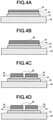
- the intermediate mold member 24 is put on the lower mold member 22, and then, the ceramic substrate 12 is arranged in the ceramic substrate housing portion 24b. Thereafter, the upper mold member 26 is put on the intermediate mold member 24. In this state, a molten metal of aluminum or an aluminum alloy is injected into the mold 20 to be cooled to produce a metal/ceramic bonding substrate (shown in FIG. 1
- portions other than portions corresponding to the shape of a circuit pattern of) the etching resist 28, second metal plate 18, graphite sheet 16 and first metal plate 14 are removed by milling in the thickness directions thereof from the surface of the etching resist 28, to cause the etching resist 28, the second metal plate 18, the graphite sheet 16 and the first metal plate 14 to have the shape of the circuit pattern as shown in FIG. 4C , except that a portion (a thin portion having a thickness of about 0.2 mm) of the first metal plate 14 on the side of the ceramic substrate 12 is caused to remain (in order to prevent the ceramic substrate 12 from being broken by the contact of a cutting tool with the ceramic substrate 12 during milling).
- a portion of the first metal plate 14 other than the portion corresponding to the shape of the circuit pattern on the surface of the ceramic substrate 12 is etched with an etching solution, such as an aqueous iron chloride solution, to be removed as shown in FIG. 4D , and then, the etching resist 28 is removed.
- an etching solution such as an aqueous iron chloride solution
- a portion required for soldering thereon a semiconductor device or the like may be plated with nickel or the like.
- the molten metal is preferably injected into the mold 20 from the sprue as follows. First, the mold 20 is moved into a bonding furnace (not shown), and the interior of the bonding furnace is caused to be in an atmosphere of nitrogen to decrease the oxygen concentration therein to 100 ppm or less, preferably 10 ppm or less. Then, the mold 20 is heated to a molten metal injecting temperature by the temperature control of a heater. Thereafter, the molten metal, which is heated to the molten metal injecting temperature and which is previously measured, is pressurized at a predetermined pressure by nitrogen gas to be injected into the mold 20 from the sprue.
- the molten metal is thus injected, it is possible to prevent large bonding defects from being produced between the metal and the ceramic.
- the molten metal is preferably cooled and solidified in the mold 20 while the molten metal therein is pressurized at a predetermined pressure by blowing nitrogen gas into the sprue from a nozzle (not shown).
- the predetermined pressure applied by nitrogen gas during the injection and cooling of the molten metal is preferably in the range of from 1 kPa to 100 kPa, more preferably in the range of from 3 kPa to 80 kPa, and most preferably in the range of from 5 kPa to 15 kPa.
- the pressure is too low, it is difficult to allow the molten metal to be injected into the mold 20. If the pressure is too high, there is some possibility that the positions of the graphite sheet 16 may be shifted and/or the mold 20 may be broken. In particular, when a high pressure of not less than 1 MPa is applied if the mold 20 of carbon is used, there is some possibility that the mold 20 may be broken and/or the molten metal may leak from the mold 20.
- FIG. 3 shows a mold 120 used for producing a modified example of the preferred embodiment of a metal/ceramic bonding substrate according to the present invention.
- the bottom surface of a recessed portion (a metal base plate forming portion) 126a which is formed on the lower surface (back surface) of an upper mold member 126, has a recessed portion (a radiating fin forming portion) 126b for forming radiating fins, so that it is possible to integrally form the radiating fins on the bottom surface of a metal base plate. Since other constructions are substantially the same constructions as those of the mold 20 of FIG. 2 , 100 is added to each of the reference numbers of portions substantially having the same constructions in FIG. 3 , and the description thereof is omitted.
- the ceramic substrate may be an oxide ceramic substrate of alumina or the like, and may be a non-oxide ceramic substrate of aluminum nitride, silicon nitride or the like.
- molten metal of aluminum having a purity of 99.9 % by weight (3N) (aluminum having a thermal conductivity of 220 to 230 W/m ⁇ K and a 0.2 % proof stress of 18 to 22 MPa) was injected into the mold from the sprue thereof, the molten metal was cooled to be solidified to obtain a metal/ceramic bonding substrate wherein an aluminum base plate having a size of 70 mm x 70 mm x 5 mm was bonded directly to one side of the ceramic substrate, the other side of the ceramic substrate being bonded directly to one side of a first aluminum plate for circuit pattern having a size of 46 mm 46 mm x 0.35 mm, and wherein one side of the graphite sheet was bonded directly to the other side of the first aluminum plate, the other side of the graphite sheet being bonded directly to a second aluminum plate for circuit pattern having a size of 46 mm x 46 mm x 0.2 mm (the total thickness of the first aluminum aluminum
- a portion of aluminum corresponding to the molten metal passage (sprue runner) was removed, and the surface of the second aluminum plate was buff-polished. Then, an etching resist was formed on the buff-polished surface of the second aluminum plate. Thereafter, (portions other than portions corresponding to the shape of a circuit pattern of) the etching resist, second aluminum plate, graphite sheet and first aluminum plate were removed by milling in thickness directions thereof from the surface of the etching resist by means of a ⁇ 2mm end mill to cause them to have the shape of the circuit pattern, except that a portion of the first aluminum plate having a thickness of 0.2 mm from the side of the ceramic substrate was caused to remain.
- the portion of the first aluminum plate other than the portion corresponding to the shape of the circuit pattern on the surface of the ceramic substrate was etched with an aqueous iron chloride solution to be removed, and then, the etching resist was removed to obtain a metal/ceramic bonding substrate having the circuit pattern (of the first aluminum plate, graphite sheet and second aluminum plate) having a size of 45 mm x 45 mm x 0.6 mm.
- the (initial) surface roughness Ra of the surface of the second aluminum plate of each of the metal/ceramic bonding substrates was measured by means of a laser microscope (Super-Depth Surface Profile Measuring Microscope VK-8500 produced by Keyence Corporation). As a result, the (initial) surface roughness Ra thereof was 1.2 ⁇ m on average.
- the (initial) difference in level caused on the grain boundaries of aluminum was measured by the laser microscope. As a result, the difference in level on the grain boundaries was not larger than 10 ⁇ m at most.
- the surface roughness Ra of the surface of the second aluminum plate was measured by the same method as the above-described method. As a result, the surface roughness Ra thereof was 1.5 ⁇ m on average.
- the difference in level caused on the grain boundaries of aluminum was measured by the same method as the above-described method. As a result, the difference in level on the grain boundaries was not larger than 30 ⁇ m at most.
- the surface roughness Ra of the surface of the second aluminum plate, and the difference in level caused on the grain boundaries of aluminum were measured by the same methods as those in Example 1.
- the initial surface roughness Ra was 1.2 ⁇ m on average, and the initial difference in level on the grain boundaries was not larger than 10 ⁇ m at most.
- the surface roughness Ra after the heat cycles was 1.5 ⁇ m on average, and the difference in level on the grain boundaries after the heat cycles was not larger than 30 ⁇ m at most.
- the surface roughness Ra of the surface of the second aluminum plate, and the difference in level caused on the grain boundaries of aluminum were measured by the same methods as those in Example 1.
- the initial surface roughness Ra was 1.3 ⁇ m on average, and the initial difference in level on the grain boundaries was not larger than 10 ⁇ m at most.
- the surface roughness Ra after the heat cycles was 1.5 ⁇ m on average, and the difference in level on the grain boundaries after the heat cycles was not larger than 30 ⁇ m at most.
- the surface roughness Ra of the surface of the second aluminum plate, and the difference in level caused on the grain boundaries of aluminum were measured by the same methods as those in Example 1.
- the initial surface roughness Ra was 1.2 ⁇ m on average, and the initial difference in level on the grain boundaries was not larger than 10 ⁇ m at most.
- the surface roughness Ra after the heat cycles was 1.4 ⁇ m on average, and the difference in level on the grain boundaries after the heat cycles was not larger than 20 ⁇ m at most.
- the surface roughness Ra of the surface of the second aluminum plate, and the difference in level caused on the grain boundaries of aluminum were measured by the same methods as those in Example 2.
- the initial surface roughness Ra was 1.2 ⁇ m on average, and the initial difference in level on the grain boundaries was not larger than 10 ⁇ m at most.
- the surface roughness Ra after the heat cycles was 1.4 ⁇ m on average, and the difference in level on the grain boundaries after the heat cycles was not larger than 20 ⁇ m at most.
- the surface roughness Ra of the surface of the second aluminum plate, and the difference in level caused on the grain boundaries of aluminum were measured by the same methods as those in Example 3.
- the initial surface roughness Ra was 1.3 ⁇ m on average, and the initial difference in level on the grain boundaries was not larger than 10 ⁇ m at most.
- the surface roughness Ra after the heat cycles was 1.4 ⁇ m on average, and the difference in level on the grain boundaries after the heat cycles was not larger than 20 ⁇ m at most.
- the surface roughness Ra of the surface of the aluminum plate, and the difference in level caused on the grain boundaries of aluminum were measured by the same methods as those in Example 1.
- the initial surface roughness Ra was 1.2 ⁇ m on average, and the initial difference in level on the grain boundaries was not larger than 10 ⁇ m at most.
- the surface roughness Ra after the heat cycles was 1.9 ⁇ m on average, and the difference in level on the grain boundaries after the heat cycles was about 50 ⁇ m at most.
- the surface roughness Ra of the surface of the aluminum plate, and the difference in level caused on the grain boundaries of aluminum were measured by the same methods as those in Example 3.
- the initial surface roughness Ra was 1.3 ⁇ m on average, and the initial difference in level on the grain boundaries was not larger than 10 ⁇ m at most.
- the surface roughness Ra after the heat cycles was 2.1 ⁇ m on average, and the difference in level on the grain boundaries after the heat cycles was about 50 ⁇ m at most.
- the surface roughness Ra of the surface of the aluminum plate, and the difference in level caused on the grain boundaries of aluminum were measured by the same methods as those in Example 1.
- the initial surface roughness Ra was 1.2 ⁇ m on average, and the initial difference in level on the grain boundaries was not larger than 10 ⁇ m at most.
- the surface roughness Ra after the heat cycles was 2.3 ⁇ m on average, and the difference in level on the grain boundaries after the heat cycles was about 80 ⁇ m at most.
- the surface roughness Ra of the surface of the aluminum plate, and the difference in level caused on the grain boundaries of aluminum were measured by the same methods as those in Example 3.
- the initial surface roughness Ra was 1.3 ⁇ m on average, and the initial difference in level on the grain boundaries was not larger than 10 ⁇ m at most.
- the surface roughness Ra after the heat cycles was 2.5 ⁇ m on average, and the difference in level on the grain boundaries after the heat cycles was about 80 ⁇ m at most.
- the initial surface roughness Ra was 1.4 ⁇ m on average, and the initial difference in level on the grain boundaries was not larger than 10 ⁇ m at most.
- the surface roughness Ra after the heat cycles was 1.5 ⁇ m on average, and the difference in level on the grain boundaries after the heat cycles was not larger than 20 ⁇ m at most.
- the initial surface roughness Ra was 1.3 ⁇ m on average, and the initial difference in level on the grain boundaries was not larger than 10 ⁇ m at most.
- the surface roughness Ra after the heat cycles was 1.4 ⁇ m on average, and the difference in level on the grain boundaries after the heat cycles was not larger than 20 ⁇ m at most.
- the surface roughness Ra of the surface of the aluminum plate, and the difference in level caused on the grain boundaries of aluminum were measured by the same methods as those in Example 7.
- the initial surface roughness Ra was 1.3 ⁇ m on average, and the initial difference in level on the grain boundaries was not larger than 10 ⁇ m at most.
- the surface roughness Ra after the heat cycles was 1.7 ⁇ m on average, and the difference in level on the grain boundaries after the heat cycles was about 50 ⁇ m at most.
- the surface roughness Ra of the surface of the aluminum plate, and the difference in level caused on the grain boundaries of aluminum were measured by the same methods as those in Example 8.
- the initial surface roughness Ra was 1.4 ⁇ m on average, and the initial difference in level on the grain boundaries was not larger than 10 ⁇ m at most.
- the surface roughness Ra after the heat cycles was 1.8 ⁇ m on average, and the difference in level on the grain boundaries after the heat cycles was about 50 ⁇ m at most.
- the surface roughness Ra of the surface of the aluminum plate, and the difference in level caused on the grain boundaries of aluminum were measured by the same methods as those in Example 11.
- the initial surface roughness Ra was 1.2 ⁇ m on average, and the initial difference in level on the grain boundaries was not larger than 10 ⁇ m at most.
- the surface roughness Ra after the heat cycles was 1.7 ⁇ m on average, and the difference in level on the grain boundaries after the heat cycles was about 50 ⁇ m at most.
- the surface roughness Ra of the surface of the aluminum plate, and the difference in level caused on the grain boundaries of aluminum were measured by the same methods as those in Example 12.
- the initial surface roughness Ra was 1.3 ⁇ m on average, and the initial difference in level on the grain boundaries was not larger than 10 ⁇ m at most.
- the surface roughness Ra after the heat cycles was 1.7 ⁇ m on average, and the difference in level on the grain boundaries after the heat cycles was about 50 ⁇ m at most.
- the difference in level on the grain boundaries after the heat cycles varies relatively widely in accordance with each of the metal/ceramic bonding substrates
- the difference in level can be suppressed so as not to be larger than 30 ⁇ m at most in examples
- the difference in level is a large difference of about 50 to 80 ⁇ m at most in comparative examples, so that the mass-production of the metal/ceramic bonding substrates in comparative examples is unsuitable.
- the heat cycle is repeatedly applied on the metal/ceramic bonding substrate wherein thick aluminum plates (the total of the thicknesses of the first and second aluminum plates is not less than 0.5 mm (preferably not less than 0.8 mm)) are bonded to the ceramic substrate, it is possible to prevent a large difference in level from being caused on portions corresponding to the grain boundaries of aluminum or the aluminum alloy, so that it is possible to provide a metal/ceramic bonding substrate having excellent thermal conductivity and/or excellent electrical conductivity.
Landscapes
- Engineering & Computer Science (AREA)
- Microelectronics & Electronic Packaging (AREA)
- Ceramic Products (AREA)
- Chemical & Material Sciences (AREA)
- Ceramic Engineering (AREA)
- Cooling Or The Like Of Semiconductors Or Solid State Devices (AREA)
Applications Claiming Priority (3)
| Application Number | Priority Date | Filing Date | Title |
|---|---|---|---|
| JP2019122001 | 2019-06-28 | ||
| JP2020092939A JP7422608B2 (ja) | 2019-06-28 | 2020-05-28 | 金属-セラミックス接合基板およびその製造方法 |
| PCT/JP2020/022998 WO2020262015A1 (fr) | 2019-06-28 | 2020-06-11 | Substrat métal-céramique assemblé et son procédé de fabrication |
Publications (2)
| Publication Number | Publication Date |
|---|---|
| EP3968366A1 true EP3968366A1 (fr) | 2022-03-16 |
| EP3968366A4 EP3968366A4 (fr) | 2023-07-12 |
Family
ID=74061909
Family Applications (1)
| Application Number | Title | Priority Date | Filing Date |
|---|---|---|---|
| EP20832352.7A Pending EP3968366A4 (fr) | 2019-06-28 | 2020-06-11 | Substrat métal-céramique assemblé et son procédé de fabrication |
Country Status (3)
| Country | Link |
|---|---|
| US (1) | US12300512B2 (fr) |
| EP (1) | EP3968366A4 (fr) |
| WO (1) | WO2020262015A1 (fr) |
Families Citing this family (2)
| Publication number | Priority date | Publication date | Assignee | Title |
|---|---|---|---|---|
| TWI768966B (zh) * | 2021-06-15 | 2022-06-21 | 許國誠 | 石墨複合層疊散熱結構及其製造方法 |
| WO2025203607A1 (fr) * | 2024-03-29 | 2025-10-02 | 株式会社Uacj | Matériau de coulée en alliage d'aluminium et procédé de production d'un matériau de coulée en alliage d'aluminium |
Family Cites Families (12)
| Publication number | Priority date | Publication date | Assignee | Title |
|---|---|---|---|---|
| JP4779178B2 (ja) | 2001-03-01 | 2011-09-28 | Dowaメタルテック株式会社 | 半導体実装用絶縁基板及びパワーモジュール |
| JP2008199057A (ja) | 2006-06-02 | 2008-08-28 | Nec Lighting Ltd | 電子機器および電子機器の製造方法 |
| CN102742008B (zh) | 2010-02-05 | 2015-07-01 | 三菱综合材料株式会社 | 功率模块用基板及功率模块 |
| JP6194734B2 (ja) | 2013-10-07 | 2017-09-13 | 富士通株式会社 | 放熱器及びその製造方法 |
| WO2015087714A1 (fr) | 2013-12-09 | 2015-06-18 | 積水化学工業株式会社 | Produit d'étanchéité pour élément d'affichage |
| CN104754913B (zh) * | 2013-12-27 | 2018-06-05 | 华为技术有限公司 | 导热复合材料片及其制作方法 |
| JP6400501B2 (ja) | 2015-02-18 | 2018-10-03 | Dowaメタルテック株式会社 | 金属−セラミックス回路基板の製造方法 |
| JP2017212316A (ja) | 2016-05-25 | 2017-11-30 | Dowaホールディングス株式会社 | 金属−セラミックス接合基板およびその製造方法 |
| TWI659828B (zh) * | 2016-07-27 | 2019-05-21 | 日商Jx金屬股份有限公司 | 附散熱用金屬材之結構物、印刷電路板、電子機器及散熱用金屬材 |
| JP6753721B2 (ja) * | 2016-07-29 | 2020-09-09 | Dowaメタルテック株式会社 | 金属−セラミックス回路基板およびその製造方法 |
| JP2018135251A (ja) | 2017-02-23 | 2018-08-30 | 三菱マテリアル株式会社 | パワーモジュール用基板の製造方法 |
| JP6940997B2 (ja) | 2017-07-31 | 2021-09-29 | Dowaメタルテック株式会社 | アルミニウム−セラミックス接合基板およびその製造方法 |
-
2020
- 2020-06-11 WO PCT/JP2020/022998 patent/WO2020262015A1/fr not_active Ceased
- 2020-06-11 EP EP20832352.7A patent/EP3968366A4/fr active Pending
- 2020-06-11 US US17/623,293 patent/US12300512B2/en active Active
Also Published As
| Publication number | Publication date |
|---|---|
| EP3968366A4 (fr) | 2023-07-12 |
| US12300512B2 (en) | 2025-05-13 |
| US20220367316A1 (en) | 2022-11-17 |
| WO2020262015A1 (fr) | 2020-12-30 |
Similar Documents
| Publication | Publication Date | Title |
|---|---|---|
| EP1345480B1 (fr) | Panneau à circuit céramique | |
| US7926543B2 (en) | Method for producing metal/ceramic bonding substrate | |
| US8745841B2 (en) | Aluminum bonding member and method for producing same | |
| EP2713391B1 (fr) | Plaque de radiation de chaleur et son procédé de production | |
| EP2680678B1 (fr) | Substrat lié métal-céramique et procédé pour sa fabrication | |
| EP3968366A1 (fr) | Substrat métal-céramique assemblé et son procédé de fabrication | |
| JP5619437B2 (ja) | 金属−セラミックス接合基板の製造方法 | |
| US7131483B2 (en) | Apparatus, mold, and method for manufacturing metal-ceramic composite member | |
| EP1523037B1 (fr) | Procédé de fabrication d'un substrat composite métal/céramique | |
| US7130174B2 (en) | Integral-type ceramic circuit board and method of producing same | |
| EP1526569B1 (fr) | Substrat de type metal-ceramique et méthode de fabrication associée | |
| EP1518847B1 (fr) | Substrat composite aluminium-céramique et son procédé de fabrication | |
| JP7422608B2 (ja) | 金属-セラミックス接合基板およびその製造方法 | |
| US6764773B2 (en) | Heat-dissipating substrate, method for making the same, and semiconductor device including the same | |
| KR20230022132A (ko) | 세라믹 방열기판 제조방법 | |
| US20260116829A1 (en) | Aluminum/ceramic bonding substrate and method for producing same | |
| JP5380734B2 (ja) | アルミニウム接合部材 | |
| JP2022157227A (ja) | 金属-セラミックス接合基板およびその製造方法 | |
| JP7267030B2 (ja) | 金属-セラミックス接合基板およびその製造方法 | |
| JP3281331B2 (ja) | 耐熱衝撃性に優れたセラミックス−金属接合基板 | |
| JPH05167205A (ja) | 耐熱衝撃性に優れたセラミックス−金属接合基板 | |
| EP4319503A1 (fr) | Substrat lié aluminium-céramique et son procédé de fabrication | |
| JPH11204702A (ja) | 高熱伝導性放熱基板及びその製造方法 |
Legal Events
| Date | Code | Title | Description |
|---|---|---|---|
| STAA | Information on the status of an ep patent application or granted ep patent |
Free format text: STATUS: THE INTERNATIONAL PUBLICATION HAS BEEN MADE |
|
| PUAI | Public reference made under article 153(3) epc to a published international application that has entered the european phase |
Free format text: ORIGINAL CODE: 0009012 |
|
| STAA | Information on the status of an ep patent application or granted ep patent |
Free format text: STATUS: REQUEST FOR EXAMINATION WAS MADE |
|
| 17P | Request for examination filed |
Effective date: 20211208 |
|
| AK | Designated contracting states |
Kind code of ref document: A1 Designated state(s): AL AT BE BG CH CY CZ DE DK EE ES FI FR GB GR HR HU IE IS IT LI LT LU LV MC MK MT NL NO PL PT RO RS SE SI SK SM TR |
|
| DAV | Request for validation of the european patent (deleted) | ||
| DAX | Request for extension of the european patent (deleted) | ||
| REG | Reference to a national code |
Ref country code: DE Ref legal event code: R079 Free format text: PREVIOUS MAIN CLASS: H01L0023130000 Ipc: H01L0023373000 |
|
| A4 | Supplementary search report drawn up and despatched |
Effective date: 20230609 |
|
| RIC1 | Information provided on ipc code assigned before grant |
Ipc: H01L 21/48 20060101ALI20230602BHEP Ipc: H01L 23/373 20060101AFI20230602BHEP |