WO2020262711A1 - 半導体レーザ - Google Patents
半導体レーザ Download PDFInfo
- Publication number
- WO2020262711A1 WO2020262711A1 PCT/JP2020/031627 JP2020031627W WO2020262711A1 WO 2020262711 A1 WO2020262711 A1 WO 2020262711A1 JP 2020031627 W JP2020031627 W JP 2020031627W WO 2020262711 A1 WO2020262711 A1 WO 2020262711A1
- Authority
- WO
- WIPO (PCT)
- Prior art keywords
- optical resonator
- pulse
- optical
- semiconductor laser
- pulse width
- Prior art date
- Legal status (The legal status is an assumption and is not a legal conclusion. Google has not performed a legal analysis and makes no representation as to the accuracy of the status listed.)
- Ceased
Links
Images




Classifications
-
- H—ELECTRICITY
- H01—ELECTRIC ELEMENTS
- H01S—DEVICES USING THE PROCESS OF LIGHT AMPLIFICATION BY STIMULATED EMISSION OF RADIATION [LASER] TO AMPLIFY OR GENERATE LIGHT; DEVICES USING STIMULATED EMISSION OF ELECTROMAGNETIC RADIATION IN WAVE RANGES OTHER THAN OPTICAL
- H01S5/00—Semiconductor lasers
- H01S5/04—Processes or apparatus for excitation, e.g. pumping, e.g. by electron beams
- H01S5/042—Electrical excitation ; Circuits therefor
- H01S5/0425—Electrodes, e.g. characterised by the structure
- H01S5/04256—Electrodes, e.g. characterised by the structure characterised by the configuration
-
- H—ELECTRICITY
- H01—ELECTRIC ELEMENTS
- H01S—DEVICES USING THE PROCESS OF LIGHT AMPLIFICATION BY STIMULATED EMISSION OF RADIATION [LASER] TO AMPLIFY OR GENERATE LIGHT; DEVICES USING STIMULATED EMISSION OF ELECTROMAGNETIC RADIATION IN WAVE RANGES OTHER THAN OPTICAL
- H01S5/00—Semiconductor lasers
- H01S5/06—Arrangements for controlling the laser output parameters, e.g. by operating on the active medium
- H01S5/062—Arrangements for controlling the laser output parameters, e.g. by operating on the active medium by varying the potential of the electrodes
- H01S5/0625—Arrangements for controlling the laser output parameters, e.g. by operating on the active medium by varying the potential of the electrodes in multi-section lasers
- H01S5/06253—Pulse modulation
-
- H—ELECTRICITY
- H01—ELECTRIC ELEMENTS
- H01S—DEVICES USING THE PROCESS OF LIGHT AMPLIFICATION BY STIMULATED EMISSION OF RADIATION [LASER] TO AMPLIFY OR GENERATE LIGHT; DEVICES USING STIMULATED EMISSION OF ELECTROMAGNETIC RADIATION IN WAVE RANGES OTHER THAN OPTICAL
- H01S5/00—Semiconductor lasers
- H01S5/0014—Measuring characteristics or properties thereof
-
- H—ELECTRICITY
- H01—ELECTRIC ELEMENTS
- H01S—DEVICES USING THE PROCESS OF LIGHT AMPLIFICATION BY STIMULATED EMISSION OF RADIATION [LASER] TO AMPLIFY OR GENERATE LIGHT; DEVICES USING STIMULATED EMISSION OF ELECTROMAGNETIC RADIATION IN WAVE RANGES OTHER THAN OPTICAL
- H01S5/00—Semiconductor lasers
- H01S5/02—Structural details or components not essential to laser action
- H01S5/026—Monolithically integrated components, e.g. waveguides, monitoring photo-detectors, drivers
-
- H—ELECTRICITY
- H01—ELECTRIC ELEMENTS
- H01S—DEVICES USING THE PROCESS OF LIGHT AMPLIFICATION BY STIMULATED EMISSION OF RADIATION [LASER] TO AMPLIFY OR GENERATE LIGHT; DEVICES USING STIMULATED EMISSION OF ELECTROMAGNETIC RADIATION IN WAVE RANGES OTHER THAN OPTICAL
- H01S5/00—Semiconductor lasers
- H01S5/04—Processes or apparatus for excitation, e.g. pumping, e.g. by electron beams
- H01S5/042—Electrical excitation ; Circuits therefor
- H01S5/0428—Electrical excitation ; Circuits therefor for applying pulses to the laser
-
- H—ELECTRICITY
- H01—ELECTRIC ELEMENTS
- H01S—DEVICES USING THE PROCESS OF LIGHT AMPLIFICATION BY STIMULATED EMISSION OF RADIATION [LASER] TO AMPLIFY OR GENERATE LIGHT; DEVICES USING STIMULATED EMISSION OF ELECTROMAGNETIC RADIATION IN WAVE RANGES OTHER THAN OPTICAL
- H01S5/00—Semiconductor lasers
- H01S5/06—Arrangements for controlling the laser output parameters, e.g. by operating on the active medium
- H01S5/0601—Arrangements for controlling the laser output parameters, e.g. by operating on the active medium comprising an absorbing region
-
- H—ELECTRICITY
- H01—ELECTRIC ELEMENTS
- H01S—DEVICES USING THE PROCESS OF LIGHT AMPLIFICATION BY STIMULATED EMISSION OF RADIATION [LASER] TO AMPLIFY OR GENERATE LIGHT; DEVICES USING STIMULATED EMISSION OF ELECTROMAGNETIC RADIATION IN WAVE RANGES OTHER THAN OPTICAL
- H01S5/00—Semiconductor lasers
- H01S5/06—Arrangements for controlling the laser output parameters, e.g. by operating on the active medium
- H01S5/0601—Arrangements for controlling the laser output parameters, e.g. by operating on the active medium comprising an absorbing region
- H01S5/0602—Arrangements for controlling the laser output parameters, e.g. by operating on the active medium comprising an absorbing region which is an umpumped part of the active layer
-
- H—ELECTRICITY
- H01—ELECTRIC ELEMENTS
- H01S—DEVICES USING THE PROCESS OF LIGHT AMPLIFICATION BY STIMULATED EMISSION OF RADIATION [LASER] TO AMPLIFY OR GENERATE LIGHT; DEVICES USING STIMULATED EMISSION OF ELECTROMAGNETIC RADIATION IN WAVE RANGES OTHER THAN OPTICAL
- H01S5/00—Semiconductor lasers
- H01S5/06—Arrangements for controlling the laser output parameters, e.g. by operating on the active medium
- H01S5/062—Arrangements for controlling the laser output parameters, e.g. by operating on the active medium by varying the potential of the electrodes
- H01S5/06226—Modulation at ultra-high frequencies
-
- H—ELECTRICITY
- H01—ELECTRIC ELEMENTS
- H01S—DEVICES USING THE PROCESS OF LIGHT AMPLIFICATION BY STIMULATED EMISSION OF RADIATION [LASER] TO AMPLIFY OR GENERATE LIGHT; DEVICES USING STIMULATED EMISSION OF ELECTROMAGNETIC RADIATION IN WAVE RANGES OTHER THAN OPTICAL
- H01S5/00—Semiconductor lasers
- H01S5/06—Arrangements for controlling the laser output parameters, e.g. by operating on the active medium
- H01S5/062—Arrangements for controlling the laser output parameters, e.g. by operating on the active medium by varying the potential of the electrodes
- H01S5/0625—Arrangements for controlling the laser output parameters, e.g. by operating on the active medium by varying the potential of the electrodes in multi-section lasers
-
- H—ELECTRICITY
- H01—ELECTRIC ELEMENTS
- H01S—DEVICES USING THE PROCESS OF LIGHT AMPLIFICATION BY STIMULATED EMISSION OF RADIATION [LASER] TO AMPLIFY OR GENERATE LIGHT; DEVICES USING STIMULATED EMISSION OF ELECTROMAGNETIC RADIATION IN WAVE RANGES OTHER THAN OPTICAL
- H01S5/00—Semiconductor lasers
- H01S5/30—Structure or shape of the active region; Materials used for the active region
- H01S5/34—Structure or shape of the active region; Materials used for the active region comprising quantum well or superlattice structures, e.g. single quantum well [SQW] lasers, multiple quantum well [MQW] lasers or graded index separate confinement heterostructure [GRINSCH] lasers
-
- H—ELECTRICITY
- H01—ELECTRIC ELEMENTS
- H01S—DEVICES USING THE PROCESS OF LIGHT AMPLIFICATION BY STIMULATED EMISSION OF RADIATION [LASER] TO AMPLIFY OR GENERATE LIGHT; DEVICES USING STIMULATED EMISSION OF ELECTROMAGNETIC RADIATION IN WAVE RANGES OTHER THAN OPTICAL
- H01S5/00—Semiconductor lasers
- H01S5/30—Structure or shape of the active region; Materials used for the active region
- H01S5/34—Structure or shape of the active region; Materials used for the active region comprising quantum well or superlattice structures, e.g. single quantum well [SQW] lasers, multiple quantum well [MQW] lasers or graded index separate confinement heterostructure [GRINSCH] lasers
- H01S5/343—Structure or shape of the active region; Materials used for the active region comprising quantum well or superlattice structures, e.g. single quantum well [SQW] lasers, multiple quantum well [MQW] lasers or graded index separate confinement heterostructure [GRINSCH] lasers in AIIIBV compounds, e.g. AlGaAs-laser, InP-based laser
- H01S5/34313—Structure or shape of the active region; Materials used for the active region comprising quantum well or superlattice structures, e.g. single quantum well [SQW] lasers, multiple quantum well [MQW] lasers or graded index separate confinement heterostructure [GRINSCH] lasers in AIIIBV compounds, e.g. AlGaAs-laser, InP-based laser with a well layer having only As as V-compound, e.g. AlGaAs, InGaAs
- H01S5/3432—Structure or shape of the active region; Materials used for the active region comprising quantum well or superlattice structures, e.g. single quantum well [SQW] lasers, multiple quantum well [MQW] lasers or graded index separate confinement heterostructure [GRINSCH] lasers in AIIIBV compounds, e.g. AlGaAs-laser, InP-based laser with a well layer having only As as V-compound, e.g. AlGaAs, InGaAs the whole junction comprising only (AI)GaAs
-
- H—ELECTRICITY
- H01—ELECTRIC ELEMENTS
- H01S—DEVICES USING THE PROCESS OF LIGHT AMPLIFICATION BY STIMULATED EMISSION OF RADIATION [LASER] TO AMPLIFY OR GENERATE LIGHT; DEVICES USING STIMULATED EMISSION OF ELECTROMAGNETIC RADIATION IN WAVE RANGES OTHER THAN OPTICAL
- H01S2301/00—Functional characteristics
- H01S2301/17—Semiconductor lasers comprising special layers
- H01S2301/176—Specific passivation layers on surfaces other than the emission facet
-
- H—ELECTRICITY
- H01—ELECTRIC ELEMENTS
- H01S—DEVICES USING THE PROCESS OF LIGHT AMPLIFICATION BY STIMULATED EMISSION OF RADIATION [LASER] TO AMPLIFY OR GENERATE LIGHT; DEVICES USING STIMULATED EMISSION OF ELECTROMAGNETIC RADIATION IN WAVE RANGES OTHER THAN OPTICAL
- H01S5/00—Semiconductor lasers
- H01S5/02—Structural details or components not essential to laser action
- H01S5/026—Monolithically integrated components, e.g. waveguides, monitoring photo-detectors, drivers
- H01S5/0265—Intensity modulators
-
- H—ELECTRICITY
- H01—ELECTRIC ELEMENTS
- H01S—DEVICES USING THE PROCESS OF LIGHT AMPLIFICATION BY STIMULATED EMISSION OF RADIATION [LASER] TO AMPLIFY OR GENERATE LIGHT; DEVICES USING STIMULATED EMISSION OF ELECTROMAGNETIC RADIATION IN WAVE RANGES OTHER THAN OPTICAL
- H01S5/00—Semiconductor lasers
- H01S5/20—Structure or shape of the semiconductor body to guide the optical wave ; Confining structures perpendicular to the optical axis, e.g. index or gain guiding, stripe geometry, broad area lasers, gain tailoring, transverse or lateral reflectors, special cladding structures, MQW barrier reflection layers
- H01S5/22—Structure or shape of the semiconductor body to guide the optical wave ; Confining structures perpendicular to the optical axis, e.g. index or gain guiding, stripe geometry, broad area lasers, gain tailoring, transverse or lateral reflectors, special cladding structures, MQW barrier reflection layers having a ridge or stripe structure
Definitions
- the present invention relates to a semiconductor laser.
- Patent Document 1 proposes a GaAs / AlGaAs semiconductor laser.
- An object of the present invention is to provide a semiconductor laser that generates ultrashort pulses.
- a pulse injection means for injecting excitation energy into the optical resonator with a time width of sub-nanoseconds is provided.
- the optical resonator has a multi-section structure separated into a gain region and an absorption region.
- a semiconductor laser that generates an optical pulse with a pulse width shorter than 2.5 times the photon lifetime of the optical resonator.
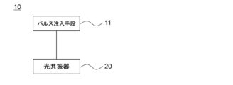
- FIG. 1 is a schematic configuration diagram of a semiconductor laser 10 according to the first embodiment of the present invention.
- FIG. 2A is a vertical cross-sectional view of the optical resonator 20 according to the first embodiment of the present invention along the longitudinal direction.
- FIG. 2B is a cross-sectional view perpendicular to the longitudinal direction of the optical resonator 20 according to the first embodiment of the present invention.
- FIG. 3 is a vertical cross-sectional view of the light emitting layer 23 according to the first embodiment of the present invention along the longitudinal direction.
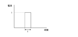
- FIG. 4 is a schematic diagram of a pulse current applied to the optical resonator 20 according to the first embodiment of the present invention.
- FIG. 1 is a schematic configuration diagram of a semiconductor laser 10 according to the first embodiment of the present invention.
- FIG. 2A is a vertical cross-sectional view of the optical resonator 20 according to the first embodiment of the present invention along the longitudinal direction.
- FIG. 2B is a cross-sectional view perpendicular to
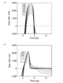
- FIG. 5A is a graph showing the gain absorption change in the time domain in the laser oscillation spectrum of the first embodiment of the present invention.
- FIG. 5B is a graph showing the gain absorption change in the time domain in the laser oscillation spectrum of the semiconductor laser of the comparative form.
- FIG. 6 is a graph showing an example of the relationship between the time width t of the pulse current applied to the optical resonator 20 according to the first embodiment of the present invention and the pulse width of the generated optical pulse.
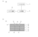
- FIG. 7A is a schematic configuration diagram of the semiconductor laser 70 according to the first modification of the first embodiment of the present invention.
- FIG. 7B is a vertical cross-sectional view of the optical resonator 71 according to the first modification of the first embodiment of the present invention along the longitudinal direction.
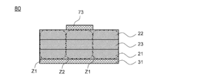
- FIG. 8 is a vertical cross-sectional view of the optical resonator 80 according to the second modification of the first embodiment of the present invention along the longitudinal direction.
- FIG. 9A is a cross-sectional view parallel to the longitudinal direction of the optical resonator 91 according to the third modification of the first embodiment of the present invention.
- FIG. 9B is a schematic cross-sectional view (cross-sectional view perpendicular to the longitudinal direction) showing an example of the optical resonator 91.
- FIG. 9C is a schematic cross-sectional view (cross-sectional view perpendicular to the longitudinal direction) showing another example of the optical resonator 91.
- an ultrashort pulse laser in which the pulse width of the generated optical pulse is from femtosecond to several picoseconds, for example, a solid-state laser using a mode-locking method is known.
- a solid-state laser is expensive and large in size, and its operation is unstable without temperature control and a clean environment. Therefore, an ultrashort pulse semiconductor laser that is low in cost, compact in size, and has high stable operation has been desired.
- a mode-locking method and a gain switching method are known as methods for generating short pulses in a semiconductor laser.
- the semiconductor laser using the gain switching method operates more stably than the mode-locking method, and the repetition frequency can be set arbitrarily.
- the lower limit of the pulse width of the generated optical pulse is theoretically limited by the photon lifetime of the optical cavity, and the pulse width of the optical pulse that can actually be generated is the optical resonator. Since it is more than 2.5 times the photon lifetime of the photon, it has been considered difficult to generate an ultrashort pulse of femtoseconds to several picoseconds.
- the inventors of the present application have conducted diligent research on the above-mentioned events.
- As a result by making the optical cavity a multi-section structure and injecting excitation energy with a time width of sub-nanoseconds, it is possible to generate an optical pulse having a pulse width shorter than 2.5 times the photon lifetime of the optical cavity. Furthermore, it has been found that an optical pulse having a pulse width shorter than the photon lifetime can be generated, and thus an ultrashort pulse of femtoseconds to several picoseconds can be stably generated.
- the present invention is based on the above findings found by the inventor and the like.
- FIG. 1 is a schematic configuration diagram of the semiconductor laser 10 of the present embodiment. As shown in FIG. 1, the semiconductor laser 10 of the present embodiment includes a pulse injection means 11 and an optical resonator 20.
- the pulse injection means 11 is configured to, for example, apply a pulse current to the optical resonator 20.
- the semiconductor laser 10 can be driven by the pulse current applied by the pulse injection means 11.
- FIG. 2A is a vertical cross-sectional view of the optical resonator 20 of the present embodiment along the longitudinal direction.
- FIG. 2B is a cross-sectional view perpendicular to the longitudinal direction of the optical resonator 20 of the present embodiment.
- the optical resonator 20 of the present embodiment has a first compound semiconductor layer 21, a second compound semiconductor layer 22, and a light emitting layer 23. There is.
- the "longitudinal direction" of the optical resonator 20 or the like means a direction parallel to the emitted light of the semiconductor laser 10, and can be rephrased as an "oscillation direction”.
- the first compound semiconductor layer 21 is provided, for example, in the lower part of the optical resonator 20.
- the first compound semiconductor layer 21 contains n-type impurities. Examples of such a first compound semiconductor layer 21 include Si-doped AlGaAs-based compound semiconductors.
- the second compound semiconductor layer 22 is provided, for example, on the upper part of the optical resonator 20.
- the second compound semiconductor layer 22 contains p-type impurities. Examples of such a second compound semiconductor layer 22 include a C-doped AlGaAs-based compound semiconductor. As shown in FIG. 2B, the second compound semiconductor layer 22 is formed with, for example, a convex portion when viewed from the longitudinal direction of the optical resonator 20.
- the light emitting layer 23 is provided between the first compound semiconductor layer 21 and the second compound semiconductor layer 22.
- the light emitting layer 23 has a multiple quantum well structure described later.
- FIG. 3 is a vertical cross-sectional view of the light emitting layer 23 along the longitudinal direction.
- the light emitting layer 23 has a multiple quantum well structure in which a plurality of well layers 24 and a plurality of barrier layers 25 are alternately laminated. Examples of the combination of (well layer 24 and barrier layer 25) include (GaAs, Al x Ga (1-x) As).
- the light emitting layer 23 has a multiple quantum well structure in which the well layer 24 and the barrier layer 25 are laminated for 5 cycles or more.
- the light emitting layer 23 having a quantum well structure of less than 5 cycles it becomes difficult to generate an optical pulse having a pulse width shorter than 2.5 times the photon lifetime pH of the optical resonator 20.
- the light emitting layer 23 has a multiple quantum well structure having five or more cycles, it is possible to generate an optical pulse having a pulse width shorter than 2.5 times the photon lifetime pH of the optical resonator 20.
- the light emitting layer 23 preferably has a multiple quantum well structure having 10 or more cycles. As a result, the pulse width of the generated optical pulse can be further shortened. It is more preferable that the light emitting layer 23 has a multiple quantum well structure having 20 cycles or more. As a result, the pulse width of the generated optical pulse can be further shortened. In addition, the peak intensity of the generated light pulse can be improved.
- the photon lifetime pH of the optical resonator 20 is defined by the following equation (1).
- vg is the group velocity.
- a in is the internal loss in transparent carrier density.
- a m is a mirror loss.
- Group velocity v g is defined by the following equation (2).
- c is the speed of light.
- ng is the group refractive index.
- the mirror losses a m is defined by the following equation (3).
- L is the cavity length.
- R 1 is the reflectance of one of the reflectors.
- R 2 is the reflectance of the other reflector.
- the photon lifetime pH is, for example, about several picoseconds.
- the photon lifetime pH of the optical resonator 20 of the present embodiment is, for example, 2 ps.
- the pulse width of the generated optical pulse is limited by the photon lifetime tph of the optical resonator, so that the optical pulse having a pulse width shorter than the photon lifetime tph can be obtained. It was considered theoretically impossible to generate. Further, the pulse width of the light pulses that can actually be generated, to stay more than 2.5 times the photon lifetime t ph of the optical resonator to generate light pulses with a short pulse width than 2.5 times the photon lifetime t ph That was considered difficult.
- the semiconductor laser 10 of the present embodiment intentionally adopts a multiple quantum well structure having five or more cycles and injects excitation energy in a time width of sub-nanoseconds, which is shorter than expected by conventional technical wisdom.
- An optical pulse having a pulse width can be generated.
- the semiconductor laser 10 of the present embodiment the semiconductor laser using the conventional gain switching method has not been achieved, is possible to generate light pulses with a short pulse width than 2.5 times the photon lifetime t ph of the optical resonator can, furthermore, it is possible to generate optical pulses having a short pulse width than photon lifetime t ph.
- the optical resonator 20 of the present embodiment has, for example, a gain region Z1 and an absorption region Z2, as shown in FIG. 2A.
- the gain region Z1 and the absorption region Z2 are alternately arranged along the longitudinal direction (oscillation direction) of the optical resonator 20.
- the gain region Z1 is arranged at both ends in the longitudinal direction of the optical resonator 20, for example, and the absorption region Z2 is arranged between the gain regions Z1.
- Such a structure in which the optical resonator has a gain region Z1 and an absorption region Z2 is called a multi-section structure. Since the optical resonator 20 has a multi-section structure, the transition from gain to absorption in the time domain in the laser oscillation spectrum can be steepened. As a result, the tail component of the generated light pulse can be reduced, and the pulse width of the generated light pulse can be shortened.
- the width of the absorption region Z2 in the longitudinal direction can be arbitrarily selected. By changing the width of the absorption region Z2 in the longitudinal direction, the pulse width and peak intensity of the generated optical pulse can be controlled.
- the width of the absorption region Z2 in the longitudinal direction is preferably 1% or more and 50% or less of the width in the longitudinal direction of the optical resonator 20. If the width of the absorption region Z2 in the longitudinal direction is less than 1% of the width in the longitudinal direction of the optical resonator 20, it is difficult to obtain the effect of shortening the pulse width of the generated optical pulse. On the other hand, by setting the width of the absorption region Z2 in the longitudinal direction to 1% or more of the width in the longitudinal direction of the optical resonator 20, the pulse width of the light pulse generated efficiently can be shortened.
- the width of the absorption region Z2 in the longitudinal direction exceeds 50% of the width in the longitudinal direction of the optical resonator 20, the peak intensity of the generated optical pulse may be lowered.
- the width of the absorption region Z2 in the longitudinal direction is set to 50% or less of the width in the longitudinal direction of the optical resonator 20, the peak intensity of the generated optical pulse can be improved.
- the optical resonator 20 of the present embodiment has, for example, a first electrode 31, a second electrode 32, and an insulating layer 33, as shown in FIG. 2 (b).
- the first electrode 31 is provided so as to cover the first compound semiconductor layer 21, for example, and is electrically connected to the first compound semiconductor layer 21.
- the second electrode 32 is provided, for example, so as to cover a part of the second compound semiconductor layer 22, and is electrically connected to the second compound semiconductor layer 22. As shown in FIG. 2A, the second electrode 32 is located above the gain region Z1.
- the insulating layer 33 is provided on both sides of the convex portion of the second compound semiconductor layer 22, for example, when viewed from the longitudinal direction of the optical resonator 20.
- the first electrode 31 and the second electrode 32 are configured to be connected to the pulse injection means 11.
- the insulating layer 33 functions as a dielectric of a capacitor for reducing the stray capacitance of the optical resonator 20.
- an insulating layer 33 for example, an insulator such as polyimide can be used.
- the insulating layer 33 is preferably configured so that the stray capacitance of the optical resonator 20 is sufficiently small.
- the semiconductor laser 10 can be driven at high speed. Specifically, for example, it is possible to inject excitation energy into the optical resonator 20 with a time width of sub-nanoseconds. That is, it is preferable to configure the insulating layer 33 so that the excitation energy can be injected into the optical resonator 20 with a time width of sub-nanoseconds.
- the area of the second electrode 32 is sufficiently small. By reducing the area of the second electrode 32, the semiconductor laser 10 can be driven at high speed. Specifically, for example, it is possible to inject excitation energy into the optical resonator 20 with a time width of sub-nanoseconds. That is, it is preferable to set the area of the second electrode 32 so that the excitation energy can be injected into the optical resonator 20 with a time width of sub-nanoseconds.
- the optical resonator 20 of this embodiment has the above-mentioned electrode structure. This makes it possible to inject excitation energy into the gain region Z1 of the optical resonator 20 with a time width of sub-nanoseconds.
- FIG. 4 is a schematic diagram of the pulse current applied to the optical resonator 20.
- the pulse current applied to the optical resonator 20 is, for example, a rectangular pulse current having a time width t and a height i.
- the pulse injection means 11 can apply the above-mentioned pulse current to the optical resonator 20 at an arbitrary timing.
- the time width t of the pulse current applied to the optical resonator 20 is sub-nanoseconds, specifically less than 1 ns. By setting the time width t of the pulse current to less than 1 ns, it is possible to generate an optical pulse having a pulse width shorter than 2.5 times the photon lifetime pH of the optical resonator 20.
- the height of the pulse current applied to the optical resonator 20 i is preferably at least twice the threshold current i th steady oscillation of the optical resonator 20. It is less than twice the height i is the threshold current i th pulse current, fast carrier dynamics hardly realized. On the contrary, by setting the pulse current height i at least twice the threshold current i th, it is possible to realize a high-speed carrier dynamics. As a result, the gain absorption change in the time domain in the laser oscillation spectrum can be steepened, and the pulse width of the generated optical pulse can be shortened.
- the height i of the pulse current is more preferably 5 times or more of the threshold current i th. As a result, the pulse width of the generated optical pulse can be further shortened.
- FIG. 5A is a graph showing the gain absorption change in the time domain in the laser oscillation spectrum of the semiconductor laser having the multiple quantum well structure and the multi-section structure according to the present embodiment.
- FIG. 5B is a graph showing the gain absorption change in the time domain in the laser oscillation spectrum of the semiconductor laser having the double hetero structure and the single section structure according to the comparative form.
- a positive value on the vertical axis indicates a gain, and a negative value indicates absorption.
- the change from gain to absorption is not steep, and the transition is trailing. Therefore, the tail component of the generated optical pulse becomes large, and the pulse width of the generated optical pulse may become long.
- the change from gain to absorption is steep in all energy bands (0.000 eV to 0.200 eV), and the rise and fall are steep. Are both sharp transitions. Therefore, the tail component of the generated light pulse can be reduced, and the pulse width of the generated light pulse can be shortened.
- the inventors of the present application have also confirmed that the pulse width of the generated optical pulse can be shortened by at least one of the multiple quantum well structure and the multi-section structure as compared with the comparative form.
- FIG. 6 shows the time width t of the pulse current applied to the optical resonator 20 of the present embodiment (that is, the time width t of injecting excitation energy into the optical resonator 20), the pulse width of the generated optical pulse, and the pulse width. It is a graph which shows an example of the relationship of.
- an optical pulse having a pulse width shorter than 2.5 times the photon lifetime pH of the optical resonator 20 can be generated by the above-described configuration and driving method of the semiconductor laser 10. it can. Further, preferably, it is possible to generate an optical pulse having a pulse width shorter than the photon lifetime pH .
- the photon lifetime pH of the optical resonator 20 is 2.0 ps, and 2.5 times, 2.0 times and 1.5 times the photon lifetime pH are 5.0 ps and 4.0 ps, respectively. It is 3.0 ps.
- the pulse width of the generated optical pulse is set to the photon lifetime t ph of the optical resonator 20. It can be shortened to about 2.2 ps, which is slightly higher.
- the time width t is set to less than 1 ns (sub-nanoseconds) so that the pulse width of the generated optical pulse is shorter than 2.5 times the photon lifetime pH of the optical resonator 20. It is understood that it can be shorter than 2.0 times, more preferably shorter than 1.5 times. Further, by setting the time width t of the pulse current to less than 600 ps, for example, the pulse width of the optical pulse can be made shorter than the photon lifetime t ph of the optical resonator 20. Further, by setting the time width t of the pulse current to, for example, less than 70 ps, the pulse width of the optical pulse can be set to the femtosecond range (less than 1 ps).
- the time width t for injecting excitation energy into the optical resonator 20 within a range of, for example, less than 1 ns (sub-nanoseconds), a semiconductor laser using a conventional gain switching method can be obtained. It is possible to generate an optical pulse having a short pulse width that was not obtained.
- the time width t may be appropriately set according to the pulse width to be generated. For example, as the pulse width is shorter than 2.5 times the photon lifetime t ph of the optical resonator 20, also for example, so that the pulse width becomes shorter than the photon lifetime t ph of the optical resonator 20, also for example, pulse
- the time width t may be appropriately set as necessary so that the width is less than 1 ps.
- the time width t is set within the range of less than 1 ns (sub-nanosecond) in order to shorten the pulse width more reliably. It may be set, for example, within a range of less than 800 ps, for example, it may be set within a range of less than 700 ps, or it may be set within a range of, for example, less than 600 ps.
- it may be set in the range of less than 500 ps, it may be set in the range of less than 400 ps, for example, it may be set in the range of less than 300 ps, and it may be set in the range of less than 200 ps, for example. It may be set within the range of, for example, it may be set within the range of less than 100 ps.
- the lower limit of the time width t is not particularly limited, but is exemplified by, for example, 2 ps or more (and, for example, 10 ps or more).
- the time width t is less than 2 ps (or less than 10 ps)
- the pulse width of the optical pulse can be efficiently controlled.
- the pulse width can be shortened to about 0.4 ps.
- the optical resonator 20 of the present embodiment has a multi-section structure. This makes it possible to steep the transition from gain to absorption in the time domain in the laser oscillation spectrum. Therefore, the tail component of the generated light pulse can be reduced, and the pulse width of the generated light pulse can be shortened.
- the semiconductor laser 10 of the present embodiment the semiconductor laser using the conventional gain switching method has not been achieved, to generate light pulses with a short pulse width than 2.5 times the photon lifetime t ph of the optical resonator 20 Can be done.
- an optical pulse having a shorter pulse width of the photon lifetime pH of the optical resonator 20 can be generated.
- ultrashort pulses of femtoseconds to several picoseconds can be stably generated.
- the light emitting layer 23 of the present embodiment has a multiple quantum well structure in which a well layer 24 and a barrier layer 25 are laminated for 5 cycles or more. Therefore, it is possible to generate an optical pulse having a pulse width shorter than 2.5 times the photon lifetime pH of the optical resonator 20. Preferably, it is possible to generate an optical pulse having a pulse width shorter than the photon lifetime pH of the optical resonator 20.
- the semiconductor laser 10 of the present embodiment intentionally adopts a multiple quantum well structure having five or more cycles, and further uses an ultragain switching method, so that light having a short pulse width exceeding the expectation of conventional technical wisdom is obtained.
- a pulse can be generated.
- the semiconductor laser 10 of the present embodiment the semiconductor laser using the conventional gain switching method has not been achieved, to generate light pulses with a short pulse width than 2.5 times the photon lifetime t ph of the optical resonator 20 Can be done.
- ultrashort pulses of femtoseconds to several picoseconds can be stably generated.
- the pulse width of the generated light pulse can be further shortened. Further, by forming the light emitting layer 23 of the present embodiment into a multiple quantum well structure having 20 cycles or more, the pulse width of the generated optical pulse can be further shortened. In addition, the peak intensity of the generated light pulse can be improved.
- the insulating layer 33 of the present embodiment is preferably configured so that the stray capacitance of the optical resonator 20 is sufficiently small.
- the semiconductor laser 10 can be driven at high speed. Specifically, for example, it is possible to inject excitation energy into the optical resonator 20 with a time width of sub-nanoseconds.
- the area of the second electrode 32 of the present embodiment is preferably sufficiently small. By reducing the area of the second electrode 32, the semiconductor laser 10 can be driven at high speed. Specifically, for example, it is possible to inject excitation energy into the optical resonator 20 with a time width of sub-nanoseconds.
- the time width t of the pulse current applied to the optical resonator 20 of the present embodiment is sub-nanoseconds, specifically less than 1 ns. As a result, it is possible to generate an optical pulse having a pulse width shorter than 2.5 times the photon lifetime pH of the optical resonator 20.
- Height i of the pulse current applied to the optical resonator 20 (g) This embodiment is preferably at least twice the threshold current i th steady oscillation of the optical resonator 20. As a result, high-speed carrier dynamics can be realized. Therefore, it is possible to steep the gain absorption change in the time domain in the laser oscillation spectrum and shorten the pulse width of the generated optical pulse.
- the height i of the pulse current is more preferably 5 times or more of the threshold current i th. As a result, the pulse width of the generated optical pulse can be further shortened.
- FIG. 7A is a schematic configuration diagram of the semiconductor laser 70 of this modified example. As shown in FIG. 7A, the semiconductor laser 70 of this modification is different from the semiconductor laser 10 of the first embodiment in that it has a bias power supply 72 as a means for applying a reverse bias voltage described later. There is.
- FIG. 7B is a vertical cross-sectional view of the optical resonator 71 of this modified example along the longitudinal direction.
- the optical resonator 71 of the present modification is different from the optical resonator 20 of the first embodiment in that it has a third electrode 73.
- the third electrode 73 is provided on the upper part of the absorption region Z2 so as to cover a part of the upper part of the second compound semiconductor layer 22, and is electrically connected to the second compound semiconductor layer 22.
- a separation groove 74 is provided between the second electrode 32 and the third electrode 73 so that the second electrode 32 and the third electrode 73 do not come into electrical contact with each other.
- the bias power supply 72 is used to use the first electrode 31 and the third electrode 73.
- a voltage is applied to the absorption region Z2 of the optical resonator 71 via the above. If the pulse current applied to the gain region Z1 is forward biased, the voltage applied to the absorption region Z2 is reverse biased.
- the pulse width of the optical pulse generated by controlling the amount of the reverse bias voltage applied is finely adjusted. , Can be calibrated. This makes it possible to improve the production yield of the semiconductor laser device. In addition, the peak intensity of the generated light pulse can be controlled.
- FIG. 8 is a vertical cross-sectional view of the optical resonator 80 of the present modification along the longitudinal direction. As shown in FIG. 8, the optical resonator 80 of the present modification is different from the optical resonator 20 of the first embodiment in that it does not have the second electrode 32 and the insulating layer 33 but has the third electrode 73. It's different.
- excitation energy is injected by irradiating the optical resonator 80 with excitation light from above as a pulse injection means. At this time, since a part of the excitation light is reflected by the third electrode 73, the excitation energy from the excitation light can be injected only into the gain region Z1.
- a titanium sapphire laser can be used as the light source of the excitation light.
- the time width t of the excitation light of this modification is sub-nanoseconds, specifically less than 1 ns.
- a reverse bias voltage may be applied to the absorption region Z2 of the optical resonator 80 via the first electrode 31 and the third electrode 73, as in the modified example 1 of the first embodiment.
- FIG. 9A is a cross-sectional view of the optical resonator 91 of this modified example parallel to the longitudinal direction. As shown in FIG. 9A, the optical resonator 91 of the present modification is different from the optical resonator 20 of the first embodiment in the arrangement state of the gain region Z1 and the absorption region Z2.
- the gain region Z1 and the absorption region Z2 of this modified example intersect in the longitudinal direction of the optical resonator 91 when the optical resonator 91 is viewed in a plan view (hereinafter referred to as They are arranged alternately along the "short direction").
- the absorption region Z2 is arranged at both ends in the lateral direction of the optical resonator 91, for example, and the gain region Z1 is arranged between the absorption regions Z2.
- FIG. 9B is a schematic cross-sectional view (cross-sectional view perpendicular to the longitudinal direction) showing an example of the optical resonator 91 of this modified example.
- the third electrode 73 is provided at both ends in the lateral direction of the second compound semiconductor layer 22.
- a reverse bias voltage is applied to the absorption region Z2 of the optical resonator 91 via the first electrode 31 and the third electrode 73.
- the absorption region Z2 By applying a reverse bias voltage to the absorption region Z2, it is possible to promote light absorption in the absorption region Z2 even if the absorption region Z2 is not arranged along the oscillation direction (longitudinal direction) of the optical resonator 91. .. As a result, the tail component of the generated light pulse can be reduced, and the pulse width of the generated light pulse can be shortened. In addition, the peak intensity of the generated light pulse can be improved as compared with the first embodiment.
- FIG. 9C is a schematic cross-sectional view (cross-sectional view perpendicular to the longitudinal direction) showing another example of the optical resonator 91 of this modified example.
- the optical resonator 91 of this modified example is provided with an ion implantation region Z3, for example, in a part of the second compound semiconductor layer 22.
- the ion implantation region Z3 may be provided in a part of the light emitting layer 23, or may be provided at a boundary portion between the second compound semiconductor layer 22 and the light emitting layer 23.
- the ion implantation region Z3 is made to function as an absorption region by implanting ions into the ion implantation region Z3.
- the electrode structure can be simplified as compared with the first embodiment.
- the gain region Z1 is arranged at both ends in the longitudinal direction of the optical resonator 20 and the absorption region Z2 is arranged between the gain regions Z1 has been described.
- the absorption region Z2 is arranged at both ends of the optical resonator 91 in the lateral direction, and the gain region Z1 is arranged between the absorption regions Z2.
- the arrangement state of the gain region Z1 and the absorption region Z2 is not limited to the above-described form and can be changed in various ways.
- the gain region Z1 may be arranged at one end in the longitudinal direction of the optical resonator, and the absorption region Z2 may be arranged at the other end of the optical resonator in the longitudinal direction. Further, for example, the gain region Z1 may be arranged at one end of the optical resonator in the lateral direction, and the absorption region Z2 may be arranged at the other end of the optical resonator in the lateral direction. Further, for example, a plurality of three or more gain regions Z1 may be arranged along the longitudinal direction or the lateral direction of the optical resonator, and a plurality of absorption regions Z2 may be arranged between the gain regions Z1. Further, for example, a plurality of gain regions Z1 may be arranged in a grid pattern along the longitudinal direction and the lateral direction of the optical resonator, and a plurality of absorption regions Z2 may be arranged between the gain regions Z1.
- the pulse width and peak intensity of the generated optical pulse can be controlled by variously changing the arrangement state of the gain region Z1 and the absorption region Z2.
- a GaAs substrate was prepared, and Al 0.33 Ga 0.67 As doped with Si 6 to 7 ⁇ 10 17 cm -3 as a first compound semiconductor layer was epitaxially grown on the GaAs substrate to a thickness of 2000 nm. ..
- a well layer (GaAs) and a barrier layer (Al 0.33 Ga 0.67 As) were laminated for 50 cycles on the first compound semiconductor layer as a light emitting layer to form a multiple quantum well structure.
- the thickness of the well layer was 12 nm, and the thickness of the barrier layer was 10 nm. Therefore, the thickness of the light emitting layer was 1100 nm.
- Al 0.33 Ga 0.67 As doped with C 6 to 7 ⁇ 10 17 cm -3 as a second compound semiconductor layer was epitaxially grown to a thickness of 1700 nm.
- Sample 1 has a single section structure without an absorption region.
- the first electrode was provided below the first compound semiconductor layer. Both ends of the optical resonator in the longitudinal direction were cleaved, and the width of the optical resonator in the longitudinal direction was 250 ⁇ m. The photon lifetime of the optical resonator was 2.2 ps. From the above, the sample 1 of the optical resonator was obtained.
- Sample 2 has a multi-section structure, an absorption region of 10 ⁇ m is provided between the gain regions at both ends in the longitudinal direction of the optical resonator, and a third electrode is provided above the absorption region. Other than that, it was prepared in the same manner as Sample 1.
- Sample 3 has a multi-section structure, an absorption region of 20 ⁇ m is provided between the gain regions at both ends in the longitudinal direction of the optical resonator, and a third electrode is provided above the absorption region. Other than that, it was prepared in the same manner as Sample 1.
- Sample 4 has a multi-section structure, an absorption region of 30 ⁇ m is provided between the gain regions at both ends in the longitudinal direction of the optical resonator, and a third electrode is provided above the absorption region. Other than that, it was prepared in the same manner as Sample 1.
- Sample 5 has a multi-section structure, an absorption region of 40 ⁇ m is provided between the gain regions at both ends in the longitudinal direction of the optical resonator, and a third electrode is provided above the absorption region. Other than that, it was prepared in the same manner as Sample 1.
- Sample 6 has a multi-section structure, an absorption region of 50 ⁇ m is provided between the gain regions at both ends in the longitudinal direction of the optical resonator, and a third electrode is provided above the absorption region. Other than that, it was prepared in the same manner as Sample 1.
- Sample 7 has a multi-section structure, an absorption region of 60 ⁇ m is provided between the gain regions at both ends in the longitudinal direction of the optical resonator, and a third electrode is provided above the absorption region. Other than that, it was prepared in the same manner as Sample 1.
- Sample 8 has a multi-section structure, an absorption region of 80 ⁇ m is provided between the gain regions at both ends in the longitudinal direction of the optical resonator, and a third electrode is provided above the absorption region. Other than that, it was prepared in the same manner as Sample 1.
- the first electrode and the third electrode were connected to a bias power supply, and the semiconductor laser was driven while applying a reverse bias voltage.
- the reverse bias voltage was -2V, -4V, -8V, and -12V.
- the first electrode and the third electrode were connected to a bias power supply, and the semiconductor laser was driven while applying a reverse bias voltage.
- the reverse bias voltage was -4V, -8V, and -12V.
- the first electrode and the third electrode were connected to the bias power supply, and the semiconductor laser was driven while applying the reverse bias voltage.
- the reverse bias voltage was -8V and -12V.
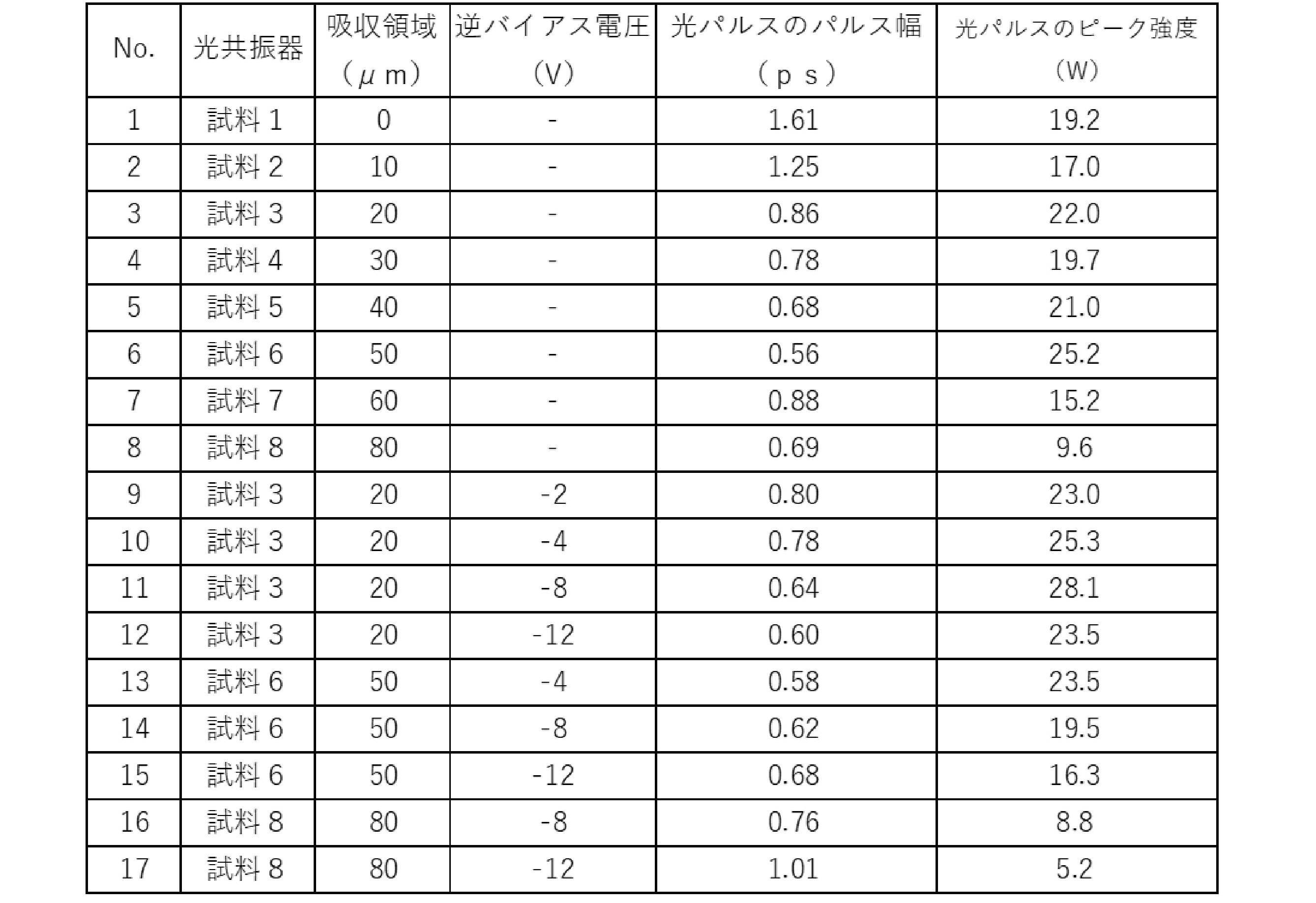
- Evaluation of pulse width and peak intensity of optical pulse Table 1 shows the results of evaluation of the pulse width and peak intensity of the optical pulse generated in (2).
- (Appendix 1) has a first compound semiconductor layer containing an n-type impurity, a second compound semiconductor layer containing a p-type impurity, and a light emitting layer provided between the first compound semiconductor layer and the second compound semiconductor layer.
- the optical resonator is provided with a pulse injection means for injecting excitation energy in a time width of sub-nanoseconds (less than 1 ns).
- the optical resonator has a multi-section structure separated into a gain region and an absorption region.
- a semiconductor laser that generates an optical pulse with a pulse width shorter than 2.5 times the photon lifetime of the optical resonator.
- the pulse width of the optical pulse is less than 2.0 times the photon lifetime. More preferably, the pulse width of the optical pulse is less than 1.5 times the photon lifetime.
- the time width is less than 600 ps. More preferably, the time width is less than 70 ps. Further, the time width may be set, for example, in the range of less than 900 ps, may be set in the range of less than 800 ps, or may be set in the range of less than 700 ps, for example.
- it may be set in the range of less than 600 ps, it may be set in the range of less than 500 ps, for example, it may be set in the range of less than 400 ps, and it may be set in the range of less than 300 ps, for example. It may be set within the range of, for example, within the range of less than 200 ps, or may be set within the range of, for example, less than 100 ps.
- Appendix 2 The semiconductor laser according to Appendix 1.
- the optical resonator has a multi-section structure separated into a gain region and an absorption region along the oscillation direction.
- the semiconductor laser according to Appendix 1 The semiconductor laser according to Appendix 1.
- the optical resonator has a multi-section structure separated into a gain region and an absorption region along a direction intersecting the oscillation direction.
- An optical pulse is generated with a pulse width shorter than the photon lifetime of the optical resonator (the time width for injecting the excitation energy is such that the pulse width of the optical pulse is shorter than the photon lifetime of the optical resonator. Is set to).
- the pulse width of the optical pulse is less than 1 ps.
- the light emitting layer has a multiple quantum well structure having five or more cycles.
- the light emitting layer has a multiple quantum well structure having 10 or more cycles. More preferably, the light emitting layer has a multiple quantum well structure having 20 cycles or more.
- Pulse injection means 20 Optical resonator 21 First compound semiconductor layer 22 Second compound semiconductor layer 23 Light emitting layer 24 Well layer 25 Barrier layer 31 First electrode 32 Second electrode 33 Insulation layer 70 Semiconductor laser 71 Optical resonator 72 Bias power supply 73 Third electrode 74 Separation groove 80 Optical resonator 91 Optical resonator Z1 Gain region Z2 Absorption region Z3 Ion injection region
Landscapes
- Physics & Mathematics (AREA)
- Condensed Matter Physics & Semiconductors (AREA)
- General Physics & Mathematics (AREA)
- Electromagnetism (AREA)
- Optics & Photonics (AREA)
- Semiconductor Lasers (AREA)
Abstract
n型不純物を含有する第1化合物半導体層と、p型不純物を含有する第2化合物半導体層と、第1化合物半導体層および第2化合物半導体層の間に設けられる発光層と、を有する光共振器と、光共振器に対して、サブナノ秒の時間幅で励起エネルギーを注入するパルス注入手段と、を備え、光共振器は、利得領域と吸収領域とに分離されたマルチセクション構造を有し、光共振器の光子寿命の2.5倍よりも短いパルス幅で光パルスを発生する半導体レーザ。
Description
本発明は、半導体レーザに関する。
半導体レーザは、光ディスクや光通信等の光源として用いられている。例えば、特許文献1には、GaAs/AlGaAs系半導体レーザが提案されている。
本発明の目的は、超短パルスを発生する半導体レーザを提供することである。
本発明の一態様によれば、
n型不純物を含有する第1化合物半導体層と、p型不純物を含有する第2化合物半導体層と、前記第1化合物半導体層および前記第2化合物半導体層の間に設けられる発光層と、を有する光共振器と、
前記光共振器に対して、サブナノ秒の時間幅で励起エネルギーを注入するパルス注入手段と、を備え、
前記光共振器は、利得領域と吸収領域とに分離されたマルチセクション構造を有し、
前記光共振器の光子寿命の2.5倍よりも短いパルス幅で光パルスを発生する半導体レーザが提供される。
n型不純物を含有する第1化合物半導体層と、p型不純物を含有する第2化合物半導体層と、前記第1化合物半導体層および前記第2化合物半導体層の間に設けられる発光層と、を有する光共振器と、
前記光共振器に対して、サブナノ秒の時間幅で励起エネルギーを注入するパルス注入手段と、を備え、
前記光共振器は、利得領域と吸収領域とに分離されたマルチセクション構造を有し、
前記光共振器の光子寿命の2.5倍よりも短いパルス幅で光パルスを発生する半導体レーザが提供される。
本発明によれば、超短パルスを発生する半導体レーザを提供することができる。
[本発明の実施形態の説明]<発明者の得た知見>
まず、発明者等が得た知見について説明する。
まず、発明者等が得た知見について説明する。
発生する光パルスのパルス幅が、フェムト秒から数ピコ秒である超短パルスレーザとしては、例えば、モード同期法を用いた固体レーザが知られている。しかしながら、このような固体レーザは、高コストかつ大型であり、温調やクリーンな環境がないと動作が不安定である。したがって、低コストかつ小型で、高安定動作をする超短パルス半導体レーザが望まれてきた。
半導体レーザにおいて、短パルスを発生させる方法としては、例えば、モード同期法や利得スイッチング法が知られている。
モード同期法を用いた半導体レーザでは、フェムト秒から数ピコ秒の超短パルスの発生報告がある。しかしながら、モード同期法を用いた半導体レーザは、ロバスト性が低く、繰り返し周波数に任意性がないという問題があった。
一方、利得スイッチング法を用いた半導体レーザは、モード同期法に比べて高安定に動作し、繰り返し周波数を任意に設定できる。しかしながら、利得スイッチング法を用いた半導体レーザでは、発生する光パルスのパルス幅の下限が光共振器の光子寿命によって理論的に制限され、また、実際に発生できる光パルスのパルス幅は光共振器の光子寿命の2.5倍以上にとどまるため、フェムト秒から数ピコ秒の超短パルス発生は困難とされていた。
本願発明者等は、上述のような事象に対して鋭意研究を行った。その結果、光共振器をマルチセクション構造とし、サブナノ秒の時間幅で励起エネルギーを注入することによって、光共振器の光子寿命の2.5倍よりも短いパルス幅を有する光パルスを発生できること、さらには、当該光子寿命よりも短いパルス幅を有する光パルスを発生できること、そしてこれにより、フェムト秒から数ピコ秒の超短パルスを安定的に発生できることを見出した。
本発明は、発明者等が見出した上記知見に基づくものである。
[本発明の実施形態の詳細]
次に、本発明の一実施形態を、以下に図面を参照しつつ説明する。なお、本発明はこれらの例示に限定されるものではなく、特許請求の範囲によって示され、特許請求の範囲と均等の意味および範囲内でのすべての変更が含まれることが意図される。
次に、本発明の一実施形態を、以下に図面を参照しつつ説明する。なお、本発明はこれらの例示に限定されるものではなく、特許請求の範囲によって示され、特許請求の範囲と均等の意味および範囲内でのすべての変更が含まれることが意図される。
<本発明の第1実施形態>(1)半導体レーザの構成
まず、本実施形態の半導体レーザ10の構成について説明する。
まず、本実施形態の半導体レーザ10の構成について説明する。
図1は、本実施形態の半導体レーザ10の概略構成図である。本実施形態の半導体レーザ10は、図1に示すように、パルス注入手段11と、光共振器20とを備えている。
パルス注入手段11は、例えば、パルス電流を光共振器20に印加するように構成されている。パルス注入手段11が印加するパルス電流によって、半導体レーザ10を駆動することができる。
図2(a)は、本実施形態の光共振器20の長手方向に沿った縦断面図である。図2(b)は、本実施形態の光共振器20の長手方向に垂直な断面図である。図2(a)および図2(b)に示すように、本実施形態の光共振器20は、第1化合物半導体層21と、第2化合物半導体層22と、発光層23とを有している。
なお、本明細書において、光共振器20等の「長手方向」とは、半導体レーザ10の放出光に平行な方向を意味し、「発振方向」と言い換えることができる。
第1化合物半導体層21は、例えば、光共振器20の下部に設けられている。第1化合物半導体層21は、n型不純物を含有している。このような第1化合物半導体層21としては、例えば、SiをドープしたAlGaAs系化合物半導体が例示される。
第2化合物半導体層22は、例えば、光共振器20の上部に設けられている。第2化合物半導体層22は、p型不純物を含有している。このような第2化合物半導体層22としては、例えば、CをドープしたAlGaAs系化合物半導体が例示される。なお、図2(b)に示すように、第2化合物半導体層22には、光共振器20の長手方向から見た際に、例えば、凸部が形成されている。
発光層23は、第1化合物半導体層21および第2化合物半導体層22の間に設けられている。発光層23は、後述する多重量子井戸構造を有している。
図3は、発光層23の長手方向に沿った縦断面図である。図3に示すように、発光層23は、複数の井戸層24と、複数の障壁層25とが交互に積層された多重量子井戸構造を有している。(井戸層24、障壁層25)の組合せとしては、例えば、(GaAs、AlxGa(1-x)As)が例示される。
発光層23は、井戸層24および障壁層25が、5周期以上積層された多重量子井戸構造を有している。5周期未満の量子井戸構造を有する発光層23を用いる場合、光共振器20の光子寿命tphの2.5倍より短いパルス幅の光パルスを発生させることが困難となる。これに対し、発光層23が5周期以上の多重量子井戸構造を有することで、光共振器20の光子寿命tphの2.5倍より短いパルス幅の光パルスを発生させることができる。発光層23は、10周期以上の多重量子井戸構造を有することが好ましい。これにより、発生する光パルスのパルス幅をより短くすることができる。発光層23は、20周期以上の多重量子井戸構造を有することがより好ましい。これにより、発生する光パルスのパルス幅をさらに短くすることができる。また、発生する光パルスのピーク強度を向上させることができる。
なお、光共振器20の光子寿命tphは、以下の式(1)で定義される。

式(1)では、vgは群速度である。ainは透明キャリア密度における内部損失である。amはミラー損失である。群速度vgは、以下の式(2)で定義される。

式(2)では、cは光速である。ngは群屈折率である。また、ミラー損失amは、以下の式(3)で定義される。

式(3)では、Lは共振器長である。R1は一方の反射鏡の反射率である。R2は他方の反射鏡の反射率である。なお、共振器長Lが数百μm程度の一般的な光共振器の場合、光子寿命tphは、例えば、数ピコ秒程度である。本実施形態の光共振器20の光子寿命tphは、具体的には、例えば、2psである。
ここで、従来の技術常識では、多重量子井戸構造の周期数を増やすと、キャリア注入量が増えるため、半導体レーザが高速動作し難くなると考えられてきた。
また、従来の利得スイッチング法を用いた半導体レーザは、発生する光パルスのパルス幅が光共振器の光子寿命tphによって制限されるため、光子寿命tphよりも短いパルス幅を有する光パルスを発生させることは理論的に不可能と考えられていた。また、実際に発生できる光パルスのパルス幅は、光共振器の光子寿命tphの2.5倍以上にとどまるため、光子寿命tphの2.5倍より短いパルス幅の光パルスを発生させることは困難とされていた。
これに対し、本実施形態の半導体レーザ10は、敢えて5周期以上の多重量子井戸構造を採用するとともに、サブナノ秒の時間幅で励起エネルギーを注入することによって、従来の技術常識の予想を超える短いパルス幅を有する光パルスを発生させることができる。本実施形態の半導体レーザ10は、従来の利得スイッチング法を用いた半導体レーザでは実現されなかった、光共振器の光子寿命tphの2.5倍より短いパルス幅の光パルスを発生させることができ、さらには、光子寿命tphより短いパルス幅の光パルスを発生させることができる。
また、本実施形態の光共振器20は、例えば、図2(a)に示すように、利得領域Z1と、吸収領域Z2とを有している。利得領域Z1および吸収領域Z2は、光共振器20の長手方向(発振方向)に沿って交互に配置されている。利得領域Z1は、例えば、光共振器20の長手方向両端部にそれぞれ配置され、吸収領域Z2は利得領域Z1の間に配置されている。このように、光共振器が利得領域Z1と、吸収領域Z2とを有する構造は、マルチセクション構造と呼ばれる。光共振器20がマルチセクション構造を有することで、レーザ発振スペクトルにおける時間領域の利得から吸収への遷移を急峻化することができる。これにより、発生する光パルスのテール成分を小さくし、発生する光パルスのパルス幅を短くすることができる。
吸収領域Z2の長手方向の幅は、任意に選択することができる。吸収領域Z2の長手方向の幅を変化させることで、発生する光パルスのパルス幅およびピーク強度を制御することができる。
吸収領域Z2の長手方向の幅は、光共振器20の長手方向の幅の1%以上50%以下とすることが好ましい。吸収領域Z2の長手方向の幅が、光共振器20の長手方向の幅の1%未満では、発生する光パルスのパルス幅を短くする効果が得られ難い。これに対し、吸収領域Z2の長手方向の幅を、光共振器20の長手方向の幅の1%以上とすることで、効率よく発生する光パルスのパルス幅を短くすることができる。一方で、吸収領域Z2の長手方向の幅が、光共振器20の長手方向の幅の50%を超えると、発生する光パルスのピーク強度が低くなる可能性がある。これに対し、吸収領域Z2の長手方向の幅を、光共振器20の長手方向の幅の50%以下とすることで、発生する光パルスのピーク強度を向上することができる。
ここで、本実施形態の光共振器20が有する電極構造について説明する。本実施形態の光共振器20は、例えば、図2(b)に示すように、第1電極31と、第2電極32と、絶縁層33とを有している。
第1電極31は、例えば、第1化合物半導体層21を覆うように設けられ、第1化合物半導体層21に電気的に接続されている。第2電極32は、例えば、第2化合物半導体層22の一部を覆うように設けられ、第2化合物半導体層22に電気的に接続されている。第2電極32は、図2(a)に示すように、利得領域Z1の上部にそれぞれ位置している。絶縁層33は、例えば、光共振器20の長手方向から見た際に、第2化合物半導体層22の凸部の両側に設けられている。第1電極31および第2電極32は、パルス注入手段11に接続されるように構成されている。
絶縁層33は、光共振器20の浮遊容量を小さくするためのキャパシタの誘電体として機能する。このような絶縁層33としては、例えば、ポリイミドなどの絶縁体を用いることができる。絶縁層33は、光共振器20の浮遊容量が充分小さくなるように構成されていることが好ましい。光共振器20の浮遊容量を小さくすることで、半導体レーザ10を高速に駆動させることができる。具体的には、例えば、光共振器20に対してサブナノ秒の時間幅で励起エネルギーを注入することが可能となる。つまり、光共振器20に対してサブナノ秒の時間幅で励起エネルギーを注入することが可能となるように、絶縁層33を構成することが好ましい。
また、第2電極32の面積は、充分小さいことが好ましい。第2電極32の面積を小さくすることで、半導体レーザ10を高速に駆動させることができる。具体的には、例えば、光共振器20に対してサブナノ秒の時間幅で励起エネルギーを注入することが可能となる。つまり、光共振器20に対してサブナノ秒の時間幅で励起エネルギーを注入することが可能となるように、第2電極32の面積を設定することが好ましい。
本実施形態の光共振器20は、上述の電極構造を有している。これにより、光共振器20の利得領域Z1に対してサブナノ秒の時間幅で励起エネルギーを注入することが可能となる。
(2)半導体レーザの駆動方法
次に、本実施形態の半導体レーザ10の駆動方法について説明する。
次に、本実施形態の半導体レーザ10の駆動方法について説明する。
図4は、光共振器20に印加するパルス電流の模式図である。図4に示すように、光共振器20に印加するパルス電流は、例えば、時間幅t、高さiの矩形状のパルス電流である。パルス注入手段11は、任意のタイミングで上述のパルス電流を光共振器20に印加することができる。
光共振器20に印加するパルス電流の時間幅tは、サブナノ秒、具体的には1ns未満である。パルス電流の時間幅tを1ns未満とすることで、光共振器20の光子寿命tphの2.5倍より短いパルス幅の光パルスを発生させることができる。
光共振器20に印加するパルス電流の高さiは、光共振器20の定常発振の閾値電流ithの2倍以上であることが好ましい。パルス電流の高さiが閾値電流ithの2倍未満では、高速なキャリアダイナミクスが実現し難くなる。これに対し、パルス電流の高さiを閾値電流ithの2倍以上とすることで、高速なキャリアダイナミクスを実現することができる。これにより、レーザ発振スペクトルにおける時間領域の利得吸収変化を急峻化し、発生する光パルスのパルス幅を短くすることができる。また、パルス電流の高さiは、閾値電流ithの5倍以上であることがより好ましい。これにより、発生する光パルスのパルス幅をさらに短くすることができる。
図5(a)は、本実施形態による、多重量子井戸構造およびマルチセクション構造を有する半導体レーザのレーザ発振スペクトルにおける時間領域の利得吸収変化を示すグラフである。図5(b)は、比較形態による、ダブルヘテロ構造およびシングルセクション構造を有する半導体レーザのレーザ発振スペクトルにおける時間領域の利得吸収変化を示すグラフである。なお、図5(a)および図5(b)において、縦軸の正の値は利得を示し、負の値は吸収を示している。
図5(b)に示すように、比較形態による半導体レーザでは、利得から吸収への変化が急峻化しておらず、尾を引くような遷移になっている。そのため、発生する光パルスのテール成分が大きくなり、発生する光パルスのパルス幅が長くなってしまう可能性がある。これに対し、図5(a)に示すように、本実施形態では、すべてのエネルギー帯(0.000eV~0.200eV)において、利得から吸収への変化が急峻化しており、立ち上がりおよび立下りが共にシャープな遷移になっている。そのため、発生する光パルスのテール成分を小さくし、発生する光パルスのパルス幅を短くすることができる。なお、多重量子井戸構造およびマルチセクション構造の少なくとも一方によって、比較形態と比べ、発生する光パルスのパルス幅を短くできることも、本願発明者等は確認している。
図6は、本実施形態の光共振器20に印加するパルス電流の時間幅t(つまり、光共振器20に対し励起エネルギーを注入する時間幅t)と、発生する光パルスのパルス幅と、の関係の一例を示すグラフである。本実施形態では、上述の半導体レーザ10の構成および駆動方法によって、図6に示すように、光共振器20の光子寿命tphの2.5倍より短いパルス幅の光パルスを発生させることができる。さらに、好ましくは、光子寿命tphより短いパルス幅の光パルスを発生させることができる。これらは、従来の技術常識の予想を超える効果であり、従来の利得スイッチング法とは異なるメカニズムが作用しているものと考えられる。このような新規のメカニズムを、本明細書では「超利得スイッチング法」と呼ぶものとする。
図6に示す例において、光共振器20の光子寿命tphは2.0psであり、その2.5倍、2.0倍および1.5倍は、それぞれ、5.0ps、4.0psおよび3.0psである。図6に示す例では、光共振器20に印加するパルス電流の時間幅tを、1ns(1000ps)とすることで、発生する光パルスのパルス幅を、光共振器20の光子寿命tphを少し上回る2.2ps程度まで短くすることができる。このことから、時間幅tを、1ns未満(サブナノ秒)とすることで、発生する光パルスのパルス幅を、光共振器20の光子寿命tphの2.5倍より短くすること、好ましくは2.0倍より短くすること、より好ましくは1.5倍より短くすることができると理解される。さらに、パルス電流の時間幅tを、例えば600ps未満とすることで、光パルスのパルス幅を、光共振器20の光子寿命tphよりも短くすることができる。また、パルス電流の時間幅tを、例えば70ps未満とすることで、光パルスのパルス幅を、フェムト秒台(1ps未満)とすることができる。
上述のように、光共振器20に対し励起エネルギーを注入する時間幅tを、例えば1ns未満(サブナノ秒)の範囲内で適宜設定することで、従来の利得スイッチング法を用いた半導体レーザでは得られなかった短いパルス幅の光パルスを発生させることができる。時間幅tは、発生させたいパルス幅に応じて、適宜設定されてよい。例えば、パルス幅が光共振器20の光子寿命tphの2.5倍より短くなるように、また例えば、パルス幅が光共振器20の光子寿命tphより短くなるように、また例えば、パルス幅が1ps未満となるように、時間幅tは、必要に応じて適宜設定されてよい。なお、時間幅tを1ns未満(サブナノ秒)の範囲内で設定する態様を例示しているが、パルス幅をより確実に短くするために、時間幅tは、例えば900ps未満の範囲内で設定されてもよいし、また例えば800ps未満の範囲内で設定されてもよいし、また例えば700ps未満の範囲内で設定されてもよいし、また例えば600ps未満の範囲内で設定されてもよいし、また例えば500ps未満の範囲内で設定されてもよいし、また例えば400ps未満の範囲内で設定されてもよいし、また例えば300ps未満の範囲内で設定されてもよいし、また例えば200ps未満の範囲内で設定されてもよいし、また例えば100ps未満の範囲内で設定されてもよい。
なお、時間幅tの下限は、特に制限されないが、例えば2ps以上(また例えば10ps以上)であることが例示される。本例において、時間幅tが2ps未満(または10ps未満)では、光パルスのパルス幅を短くする効果が飽和する。これに対し、時間幅tを2ps以上(または10ps以上)とすることで、光パルスのパルス幅を効率よく制御することができる。なお、本例では、0.4ps程度までパルス幅を短くすることができる。
(3)本実施形態に係る効果
本実施形態によれば、以下に示す1つまたは複数の効果を奏する。
本実施形態によれば、以下に示す1つまたは複数の効果を奏する。
(a)本実施形態の光共振器20は、マルチセクション構造を有している。これにより、レーザ発振スペクトルにおける時間領域の利得から吸収への遷移を急峻化することができる。したがって、発生する光パルスのテール成分を小さくし、発生する光パルスのパルス幅を短くすることができる。
ここで、従来の利得スイッチング法を用いた半導体レーザでは、上述のように、光共振器の光子寿命tphの2.5倍より短いパルス幅の光パルスを発生させることは困難とされていた。
これに対し、本実施形態では、マルチセクション構造と、超利得スイッチング法とを組み合わせることによって、従来の技術常識の予想を超える超短パルスを発生させることができる。本実施形態の半導体レーザ10は、従来の利得スイッチング法を用いた半導体レーザでは実現されなかった、光共振器20の光子寿命tphの2.5倍より短いパルス幅の光パルスを発生させることができる。好ましくは、光共振器20の光子寿命tphのより短いパルス幅の光パルスを発生させることができる。そしてこれにより、フェムト秒から数ピコ秒の超短パルスを安定的に発生させることができる。
(b)本実施形態の発光層23は、井戸層24および障壁層25が、5周期以上積層された多重量子井戸構造を有している。そのため、光共振器20の光子寿命tphの2.5倍より短いパルス幅の光パルスを発生させることができる。好ましくは、光共振器20の光子寿命tphより短いパルス幅の光パルスを発生させることができる。
ここで、従来の技術常識では、多重量子井戸構造の周期数を増やすと、キャリア注入量が増えるため、半導体レーザが高速動作し難くなると考えられてきた。
また、従来の利得スイッチング法を用いた半導体レーザは、上述のように、光共振器の光子寿命tphの2.5倍より短いパルス幅の光パルスを発生させることは困難とされていた。
これに対し、本実施形態の半導体レーザ10は、敢えて5周期以上の多重量子井戸構造を採用し、さらに超利得スイッチング法を用いることによって、従来の技術常識の予想を超える短いパルス幅を有する光パルスを発生させることができる。本実施形態の半導体レーザ10は、従来の利得スイッチング法を用いた半導体レーザでは実現されなかった、光共振器20の光子寿命tphの2.5倍より短いパルス幅の光パルスを発生させることができる。好ましくは、光共振器20の光子寿命tphより短いパルス幅の光パルスを発生させることができる。そしてこれにより、フェムト秒から数ピコ秒の超短パルスを安定的に発生させることができる。
(c)本実施形態の発光層23を10周期以上の多重量子井戸構造とすることで、発生する光パルスのパルス幅をより短くすることができる。また、本実施形態の発光層23を20周期以上の多重量子井戸構造とすることで、発生する光パルスのパルス幅をさらに短くすることができる。また、発生する光パルスのピーク強度を向上させることができる。
(d)本実施形態の絶縁層33は、光共振器20の浮遊容量が充分小さくなるように構成されていることが好ましい。光共振器20の浮遊容量を小さくすることで、半導体レーザ10を高速に駆動させることができる。具体的には、例えば、光共振器20に対してサブナノ秒の時間幅で励起エネルギーを注入することが可能となる。
(e)本実施形態の第2電極32の面積は、充分小さいことが好ましい。第2電極32の面積を小さくすることで、半導体レーザ10を高速に駆動させることができる。具体的には、例えば、光共振器20に対してサブナノ秒の時間幅で励起エネルギーを注入することが可能となる。
(f)本実施形態の光共振器20に印加するパルス電流の時間幅tは、サブナノ秒、具体的には1ns未満である。これにより、光共振器20の光子寿命tphの2.5倍より短いパルス幅の光パルスを発生させることができる。
(g)本実施形態の光共振器20に印加するパルス電流の高さiは、光共振器20の定常発振の閾値電流ithの2倍以上であることが好ましい。これにより、高速なキャリアダイナミクスを実現することができる。したがって、レーザ発振スペクトルにおける時間領域の利得吸収変化を急峻化し、発生する光パルスのパルス幅を短くすることができる。また、パルス電流の高さiは、閾値電流ithの5倍以上であることがより好ましい。これにより、発生する光パルスのパルス幅をさらに短くすることができる。
(4)第1実施形態の変形例
上述の実施形態は、必要に応じて、以下に示す変形例のように変更することができる。以下、上述の実施形態と異なる要素についてのみ説明し、上述の実施形態で説明した要素と実質的に同一の要素には、同一の符号を付してその説明を省略する。
上述の実施形態は、必要に応じて、以下に示す変形例のように変更することができる。以下、上述の実施形態と異なる要素についてのみ説明し、上述の実施形態で説明した要素と実質的に同一の要素には、同一の符号を付してその説明を省略する。
(4-1)第1実施形態の変形例1
図7(a)は、本変形例の半導体レーザ70の概略構成図である。図7(a)に示すように、本変形例の半導体レーザ70は、後述する逆バイアス電圧を印加する手段としてのバイアス電源72を有する点で、第1実施形態の半導体レーザ10とは異なっている。
図7(a)は、本変形例の半導体レーザ70の概略構成図である。図7(a)に示すように、本変形例の半導体レーザ70は、後述する逆バイアス電圧を印加する手段としてのバイアス電源72を有する点で、第1実施形態の半導体レーザ10とは異なっている。
図7(b)は、本変形例の光共振器71の長手方向に沿った縦断面図である。図7(b)に示すように、本変形例の光共振器71は、第3電極73を有する点で、第1実施形態の光共振器20とは異なっている。第3電極73は、第2化合物半導体層22の上部の一部を覆うように、吸収領域Z2の上部に設けられており、第2化合物半導体層22と電気的に接続されている。第2電極32と、第3電極73との間には、分離溝74が設けられており、第2電極32および第3電極73が電気的に接触しないように構成されている。
本変形例では、第1電極31および第2電極32を介して光共振器71の利得領域Z1にパルス電流を印加する際に、バイアス電源72を用いて、第1電極31および第3電極73を介して光共振器71の吸収領域Z2に電圧を印加する。利得領域Z1に対して印加するパルス電流を順バイアスとすると、吸収領域Z2に対して印加する電圧は逆バイアスとなる。吸収領域Z2に逆バイアス電圧を印加することで、光共振器71の作製精度に公差があったとしても、逆バイアス電圧の印加量を制御することによって発生する光パルスのパルス幅を微調整し、校正することができる。これにより、半導体レーザ装置の生産歩留まり向上が可能となる。また、発生する光パルスのピーク強度を制御することができる。
(4-2)第1実施形態の変形例2
図8は、本変形例の光共振器80の長手方向に沿った縦断面図である。図8に示すように、本変形例の光共振器80は、第2電極32および絶縁層33を有さず、第3電極73を有する点で、第1実施形態の光共振器20とは異なっている。
図8は、本変形例の光共振器80の長手方向に沿った縦断面図である。図8に示すように、本変形例の光共振器80は、第2電極32および絶縁層33を有さず、第3電極73を有する点で、第1実施形態の光共振器20とは異なっている。
本変形例では、光共振器80にパルス電流を印加する代わりに、パルス注入手段として、光共振器80に対して上方より励起光を照射することで励起エネルギーを注入する。この際、第3電極73によって励起光の一部が反射されるため、励起光による励起エネルギーを利得領域Z1のみに注入することができる。励起光の光源としては、例えば、チタンサファイアレーザを用いることができる。
本変形例の励起光の時間幅tは、サブナノ秒、具体的には1ns未満である。励起光の時間幅tを1ns未満とすることで、光共振器80の光子寿命tphの2.5倍より短いパルス幅の光パルスを発生させることができる。
本変形例においても、第1実施形態の変形例1と同様に、第1電極31および第3電極73を介して光共振器80の吸収領域Z2に逆バイアス電圧を印加してもよい。吸収領域Z2に逆バイアス電圧を印加することで、第1実施形態の変形例1と同様の効果が得られる。
本変形例では、励起光によって光共振器80に励起エネルギーを注入するため、第2電極32や絶縁層33を設ける必要がなく、電極構造を単純化することができる。これにより、第1実施形態と比べて、より簡便に実施をすることが可能となる。
(4-3)第1実施形態の変形例3
図9(a)は、本変形例の光共振器91の長手方向に平行な横断面図である。図9(a)に示すように、本変形例の光共振器91は、利得領域Z1および吸収領域Z2の配置状態が第1実施形態の光共振器20とは異なっている。
図9(a)は、本変形例の光共振器91の長手方向に平行な横断面図である。図9(a)に示すように、本変形例の光共振器91は、利得領域Z1および吸収領域Z2の配置状態が第1実施形態の光共振器20とは異なっている。
本変形例の利得領域Z1および吸収領域Z2は、例えば、図9(a)に示すように、光共振器91を平面視した際に、光共振器91の長手方向に交差する方向(以下、「短手方向」という)に沿って交互に配置されている。吸収領域Z2は、例えば、光共振器91の短手方向両端部にそれぞれ配置され、利得領域Z1は吸収領域Z2の間に配置されている。
図9(b)は、本変形例の光共振器91の一例を示す概略断面図(長手方向に垂直な断面図)である。図9(b)に示すように、本変形例の光共振器91は、例えば、第3電極73が、第2化合物半導体層22の短手方向両端部に設けられている。本変形例では、第1電極31および第3電極73を介して光共振器91の吸収領域Z2に逆バイアス電圧を印加する。吸収領域Z2に逆バイアス電圧を印加することで、吸収領域Z2が光共振器91の発振方向(長手方向)に沿って配置されていなくても、吸収領域Z2の光吸収を促進することができる。これにより、発生する光パルスのテール成分を小さくし、発生する光パルスのパルス幅を短くすることができる。また、第1実施形態と比べて、発生する光パルスのピーク強度を向上させることができる。
図9(c)は、本変形例の光共振器91の他の例を示す概略断面図(長手方向に垂直な断面図)である。図9(c)に示すように、本変形例の光共振器91は、例えば、第2化合物半導体層22の一部に、イオン注入領域Z3が設けられている。イオン注入領域Z3は、発光層23の一部に設けられてもよいし、第2化合物半導体層22および発光層23の境界部に設けられてもよい。本変形例では、イオン注入領域Z3にイオン注入を行うことによって、イオン注入領域Z3を吸収領域として機能させる。これにより、発生する光パルスのテール成分を小さくし、発生する光パルスのパルス幅を短くすることができる。また、第1実施形態と比べて、電極構造を単純化することができる。
<本発明の他の実施形態>
以上、本発明の実施形態について具体的に説明したが、本開示は上述の実施形態に限定されるものではなく、その要旨を逸脱しない範囲で種々変更可能である。
以上、本発明の実施形態について具体的に説明したが、本開示は上述の実施形態に限定されるものではなく、その要旨を逸脱しない範囲で種々変更可能である。
例えば、上述の第1実施形態では、利得領域Z1が光共振器20の長手方向両端部にそれぞれ配置され、吸収領域Z2は利得領域Z1の間に配置されている場合について説明した。また、例えば、上述の第1実施形態の変形例3では、吸収領域Z2が光共振器91の短手方向両端部にそれぞれ配置され、利得領域Z1は吸収領域Z2の間に配置されている場合について説明した。しかしながら、利得領域Z1および吸収領域Z2の配置状態は、上述の形態に限らず種々変更可能である。
例えば、利得領域Z1が光共振器の長手方向の一端に配置され、吸収領域Z2が光共振器の長手方向の他端に配置されてもよい。また、例えば、利得領域Z1が光共振器の短手方向の一端に配置され、吸収領域Z2が光共振器の短手方向の他端に配置されてもよい。また、例えば、3個以上の利得領域Z1が光共振器の長手方向または短手方向に沿って複数配置され、吸収領域Z2が利得領域Z1の間にそれぞれ複数配置されてもよい。また、例えば、利得領域Z1が光共振器の長手方向および短手方向に沿って、格子状に複数配置され、吸収領域Z2が利得領域Z1の間にそれぞれ複数配置されてもよい。
上述のように、利得領域Z1および吸収領域Z2の配置状態を種々変更することで、発生する光パルスのパルス幅およびピーク強度を制御することができる。
次に、本発明に係る実施例を説明する。これらの実施例は本発明の一例であって、本発明はこれらの実施例により限定されない。
(1)光共振器の作製
以下のように、光共振器の試料1を作製した。
以下のように、光共振器の試料1を作製した。
GaAs基板を用意し、GaAs基板の上に、第1化合物半導体層として、Siを6~7×1017cm-3ドープしたAl0.33Ga0.67Asを2000nmの厚さにエピタキシャル成長させた。
第1化合物半導体層の上に、発光層として、井戸層(GaAs)および障壁層(Al0.33Ga0.67As)を50周期積層して、多重量子井戸構造を構成した。井戸層の厚さはそれぞれ12nm、障壁層の厚さはそれぞれ10nmとした。よって、発光層の厚さは1100nmとなった。
発光層の上に、第2化合物半導体層として、Cを6~7×1017cm-3ドープしたAl0.33Ga0.67Asを1700nmの厚さにエピタキシャル成長させた。
試料1は、吸収領域を設けず、シングルセクション構造とした。第1電極を第1化合物半導体層の下部に設けた。光共振器の長手方向両端部をへき開面とし、光共振器の長手方向の幅を250μmとした。光共振器の光子寿命は2.2psであった。以上により、光共振器の試料1を得た。
試料2は、マルチセクション構造とし、光共振器の長手方向両端部の利得領域の間に、10μmの吸収領域を設け、第3電極を吸収領域の上部に設けた。それ以外は試料1と同様に作製した。
試料3は、マルチセクション構造とし、光共振器の長手方向両端部の利得領域の間に、20μmの吸収領域を設け、第3電極を吸収領域の上部に設けた。それ以外は試料1と同様に作製した。
試料4は、マルチセクション構造とし、光共振器の長手方向両端部の利得領域の間に、30μmの吸収領域を設け、第3電極を吸収領域の上部に設けた。それ以外は試料1と同様に作製した。
試料5は、マルチセクション構造とし、光共振器の長手方向両端部の利得領域の間に、40μmの吸収領域を設け、第3電極を吸収領域の上部に設けた。それ以外は試料1と同様に作製した。
試料6は、マルチセクション構造とし、光共振器の長手方向両端部の利得領域の間に、50μmの吸収領域を設け、第3電極を吸収領域の上部に設けた。それ以外は試料1と同様に作製した。
試料7は、マルチセクション構造とし、光共振器の長手方向両端部の利得領域の間に、60μmの吸収領域を設け、第3電極を吸収領域の上部に設けた。それ以外は試料1と同様に作製した。
試料8は、マルチセクション構造とし、光共振器の長手方向両端部の利得領域の間に、80μmの吸収領域を設け、第3電極を吸収領域の上部に設けた。それ以外は試料1と同様に作製した。
(2)半導体レーザの駆動
(1)で作製した試料1~試料8に対して、チタンサファイアレーザを用いて、励起光を照射し、半導体レーザを駆動させた。励起光のパルス幅は2psとし、励起強度は光共振器の閾値の14倍とした。
(1)で作製した試料1~試料8に対して、チタンサファイアレーザを用いて、励起光を照射し、半導体レーザを駆動させた。励起光のパルス幅は2psとし、励起強度は光共振器の閾値の14倍とした。
また、試料3に対しては、第1電極および第3電極をバイアス電源に接続し、逆バイアス電圧を印加しながら半導体レーザを駆動させた。逆バイアス電圧は-2V、-4V、-8V、-12Vとした。
また、試料6に対しては、第1電極および第3電極をバイアス電源に接続し、逆バイアス電圧を印加しながら半導体レーザを駆動させた。逆バイアス電圧は-4V、-8V、-12Vとした。
また、試料8に対しては、第1電極および第3電極をバイアス電源に接続し、逆バイアス電圧を印加しながら半導体レーザを駆動させた。逆バイアス電圧は-8V、-12Vとした。
(3)光パルスのパルス幅およびピーク強度の評価
(2)で発生させた光パルスのパルス幅およびピーク強度の評価を行った結果を、表1に示す。
(2)で発生させた光パルスのパルス幅およびピーク強度の評価を行った結果を、表1に示す。
(3-1)光パルスのパルス幅の評価
No.1では、光共振器の光子寿命(2.2ps)より短いパルス幅の光パルス(1.61ps)を発生させることができた。すなわち、多重量子井戸構造を採用し、超利得スイッチング法を用いることで、光共振器の光子寿命より短いパルス幅の光パルスが発生することを確認した。なお、本実施例では50周期の多重量子井戸構造を採用しているが、本願発明者等は、5周期以上の多重量子井戸構造を採用し、超利得スイッチング法を用いることで、光共振器の光子寿命の2.5倍より短いパルス幅の光パルスが発生すること、さらに、光共振器の光子寿命より短いパルス幅の光パルスが発生することを確認している。
No.1では、光共振器の光子寿命(2.2ps)より短いパルス幅の光パルス(1.61ps)を発生させることができた。すなわち、多重量子井戸構造を採用し、超利得スイッチング法を用いることで、光共振器の光子寿命より短いパルス幅の光パルスが発生することを確認した。なお、本実施例では50周期の多重量子井戸構造を採用しているが、本願発明者等は、5周期以上の多重量子井戸構造を採用し、超利得スイッチング法を用いることで、光共振器の光子寿命の2.5倍より短いパルス幅の光パルスが発生すること、さらに、光共振器の光子寿命より短いパルス幅の光パルスが発生することを確認している。
また、マルチセクション構造を採用したNo.2~No.8では、シングルセクション構造のNo.1(1.61ps)より短いパルス幅の光パルス(0.56~1.25ps)を発生させることができた。すなわち、マルチセクション構造を採用することで、発生する光パルスのパルス幅をさらに短くできることを確認した。また、吸収領域の幅を変えることで、発生する光パルスのパルス幅を制御できることを確認した。
また、吸収領域に逆バイアス電圧を印加したNo.9~No.12では、逆バイアス電圧を印加していないNo.3(0.86ps)より短いパルス幅の光パルス(0.60~0.80ps)を発生させることができた。また、吸収領域に逆バイアス電圧を印加したNo.13~No.15では、逆バイアス電圧を印加していないNo.6(0.56ps)より長いパルス幅の光パルス(0.58~0.68ps)を発生させることができた。また、吸収領域に逆バイアス電圧を印加したNo.16~No.17では、逆バイアス電圧を印加していないNo.8(0.69ps)より長いパルス幅の光パルス(0.76~1.01ps)を発生させることができた。以上より、逆バイアス電圧の印加量を制御することによって、発生する光パルスのパルス幅を微調整できることを確認した。
(3-2)光パルスのピーク強度の評価
No.1~No.8では、光パルスのピーク強度が9.6~25.2Wの範囲で変化した。すなわち、吸収領域の幅を変えることで、発生する光パルスのピーク強度を制御できることを確認した。
No.1~No.8では、光パルスのピーク強度が9.6~25.2Wの範囲で変化した。すなわち、吸収領域の幅を変えることで、発生する光パルスのピーク強度を制御できることを確認した。
また、吸収領域に逆バイアス電圧を印加したNo.9~No.12では、逆バイアス電圧を印加していないNo.3(22.0W)より大きいピーク強度の光パルス(23.0~28.1W)を発生させることができた。また、吸収領域に逆バイアス電圧を印加したNo.13~No.15では、逆バイアス電圧を印加していないNo.6(25.2W)より小さいピーク強度の光パルス(16.3~23.5W)を発生させることができた。また、吸収領域に逆バイアス電圧を印加したNo.16~No.17では、逆バイアス電圧を印加していないNo.8(9.6W)より小さいピーク強度の光パルス(5.2~8.8W)を発生させることができた。以上より、逆バイアス電圧の印加量を制御することによって、発生する光パルスのピーク強度を制御できることを確認した。
<本発明の好ましい態様>
以下、本発明の好ましい態様を付記する。
以下、本発明の好ましい態様を付記する。
(付記1)
本発明の一態様によれば、
n型不純物を含有する第1化合物半導体層と、p型不純物を含有する第2化合物半導体層と、前記第1化合物半導体層および前記第2化合物半導体層の間に設けられる発光層と、を有する光共振器と、
前記光共振器に対して、サブナノ秒(1ns未満)の時間幅で励起エネルギーを注入するパルス注入手段と、を備え、
前記光共振器は、利得領域と吸収領域とに分離されたマルチセクション構造を有し、
前記光共振器の光子寿命の2.5倍よりも短いパルス幅で光パルスを発生する半導体レーザが提供される。好ましくは、前記光パルスの前記パルス幅は、前記光子寿命の2.0倍よりも短い。より好ましくは、前記光パルスの前記パルス幅は、前記光子寿命の1.5倍よりも短い。好ましくは、前記時間幅は600ps未満である。より好ましくは、前記時間幅は70ps未満である。また、前記時間幅は、例えば900ps未満の範囲内で設定されてもよいし、また例えば800ps未満の範囲内で設定されてもよいし、また例えば700ps未満の範囲内で設定されてもよいし、また例えば600ps未満の範囲内で設定されてもよいし、また例えば500ps未満の範囲内で設定されてもよいし、また例えば400ps未満の範囲内で設定されてもよいし、また例えば300ps未満の範囲内で設定されてもよいし、また例えば200ps未満の範囲内で設定されてもよいし、また例えば100ps未満の範囲内で設定されてもよい。
本発明の一態様によれば、
n型不純物を含有する第1化合物半導体層と、p型不純物を含有する第2化合物半導体層と、前記第1化合物半導体層および前記第2化合物半導体層の間に設けられる発光層と、を有する光共振器と、
前記光共振器に対して、サブナノ秒(1ns未満)の時間幅で励起エネルギーを注入するパルス注入手段と、を備え、
前記光共振器は、利得領域と吸収領域とに分離されたマルチセクション構造を有し、
前記光共振器の光子寿命の2.5倍よりも短いパルス幅で光パルスを発生する半導体レーザが提供される。好ましくは、前記光パルスの前記パルス幅は、前記光子寿命の2.0倍よりも短い。より好ましくは、前記光パルスの前記パルス幅は、前記光子寿命の1.5倍よりも短い。好ましくは、前記時間幅は600ps未満である。より好ましくは、前記時間幅は70ps未満である。また、前記時間幅は、例えば900ps未満の範囲内で設定されてもよいし、また例えば800ps未満の範囲内で設定されてもよいし、また例えば700ps未満の範囲内で設定されてもよいし、また例えば600ps未満の範囲内で設定されてもよいし、また例えば500ps未満の範囲内で設定されてもよいし、また例えば400ps未満の範囲内で設定されてもよいし、また例えば300ps未満の範囲内で設定されてもよいし、また例えば200ps未満の範囲内で設定されてもよいし、また例えば100ps未満の範囲内で設定されてもよい。
(付記2)
付記1に記載の半導体レーザであって、
前記光共振器は、発振方向に沿って利得領域と吸収領域とに分離されたマルチセクション構造を有する。
付記1に記載の半導体レーザであって、
前記光共振器は、発振方向に沿って利得領域と吸収領域とに分離されたマルチセクション構造を有する。
(付記3)
付記1に記載の半導体レーザであって、
前記光共振器は、前記発振方向と交差する方向に沿って利得領域と吸収領域とに分離されたマルチセクション構造を有する。
付記1に記載の半導体レーザであって、
前記光共振器は、前記発振方向と交差する方向に沿って利得領域と吸収領域とに分離されたマルチセクション構造を有する。
(付記4)
付記1から付記3に記載の半導体レーザであって、
前記光共振器の光子寿命よりも短いパルス幅で光パルスを発生する(前記励起エネルギーを注入する前記時間幅は、前記光パルスの前記パルス幅が前記光共振器の光子寿命よりも短くなるように設定されている)。好ましくは、前記光パルスの前記パルス幅は、1ps未満である。
付記1から付記3に記載の半導体レーザであって、
前記光共振器の光子寿命よりも短いパルス幅で光パルスを発生する(前記励起エネルギーを注入する前記時間幅は、前記光パルスの前記パルス幅が前記光共振器の光子寿命よりも短くなるように設定されている)。好ましくは、前記光パルスの前記パルス幅は、1ps未満である。
(付記5)
付記1から付記4に記載の半導体レーザであって、
前記発光層は、5周期以上の多重量子井戸構造を有する。好ましくは、前記発光層は、10周期以上の多重量子井戸構造を有する。さらに好ましくは、前記発光層は、20周期以上の多重量子井戸構造を有する。
付記1から付記4に記載の半導体レーザであって、
前記発光層は、5周期以上の多重量子井戸構造を有する。好ましくは、前記発光層は、10周期以上の多重量子井戸構造を有する。さらに好ましくは、前記発光層は、20周期以上の多重量子井戸構造を有する。
(付記6)
付記1から付記5のいずれか1つに記載の半導体レーザであって、
前記吸収領域に対して逆バイアス電圧を印加する手段をさらに備える。
付記1から付記5のいずれか1つに記載の半導体レーザであって、
前記吸収領域に対して逆バイアス電圧を印加する手段をさらに備える。
10 半導体レーザ
11 パルス注入手段
20 光共振器
21 第1化合物半導体層
22 第2化合物半導体層
23 発光層
24 井戸層
25 障壁層
31 第1電極
32 第2電極
33 絶縁層
70 半導体レーザ
71 光共振器
72 バイアス電源
73 第3電極
74 分離溝
80 光共振器
91 光共振器
Z1 利得領域
Z2 吸収領域
Z3 イオン注入領域
11 パルス注入手段
20 光共振器
21 第1化合物半導体層
22 第2化合物半導体層
23 発光層
24 井戸層
25 障壁層
31 第1電極
32 第2電極
33 絶縁層
70 半導体レーザ
71 光共振器
72 バイアス電源
73 第3電極
74 分離溝
80 光共振器
91 光共振器
Z1 利得領域
Z2 吸収領域
Z3 イオン注入領域
Claims (5)
- n型不純物を含有する第1化合物半導体層と、p型不純物を含有する第2化合物半導体層と、前記第1化合物半導体層および前記第2化合物半導体層の間に設けられる発光層と、を有する光共振器と、
前記光共振器に対して、サブナノ秒の時間幅で励起エネルギーを注入するパルス注入手段と、を備え、
前記光共振器は、利得領域と吸収領域とに分離されたマルチセクション構造を有し、
前記光共振器の光子寿命の2.5倍よりも短いパルス幅で光パルスを発生する半導体レーザ。 - 前記光共振器は、発振方向に沿って利得領域と吸収領域とに分離されたマルチセクション構造を有する請求項1に記載の半導体レーザ。
- 前記光共振器の光子寿命よりも短いパルス幅で光パルスを発生する請求項1または請求項2に記載の半導体レーザ。
- 前記発光層は、5周期以上の多重量子井戸構造を有する請求項1から請求項3のいずれか1項に記載の半導体レーザ。
- 前記吸収領域に対して逆バイアス電圧を印加する手段をさらに備える請求項1から請求項4のいずれか1項に記載の半導体レーザ。
Priority Applications (3)
| Application Number | Priority Date | Filing Date | Title |
|---|---|---|---|
| EP20833403.7A EP3993183A4 (en) | 2019-06-25 | 2020-08-21 | Semiconductor laser |
| US17/622,581 US12341319B2 (en) | 2019-06-25 | 2020-08-21 | Semiconductor laser |
| CN202080060812.9A CN114402492A (zh) | 2019-06-25 | 2020-08-21 | 半导体激光器 |
Applications Claiming Priority (2)
| Application Number | Priority Date | Filing Date | Title |
|---|---|---|---|
| JP2019-117574 | 2019-06-25 | ||
| JP2019117574A JP6893365B2 (ja) | 2019-06-25 | 2019-06-25 | 半導体レーザ |
Publications (1)
| Publication Number | Publication Date |
|---|---|
| WO2020262711A1 true WO2020262711A1 (ja) | 2020-12-30 |
Family
ID=74061741
Family Applications (1)
| Application Number | Title | Priority Date | Filing Date |
|---|---|---|---|
| PCT/JP2020/031627 Ceased WO2020262711A1 (ja) | 2019-06-25 | 2020-08-21 | 半導体レーザ |
Country Status (5)
| Country | Link |
|---|---|
| US (1) | US12341319B2 (ja) |
| EP (1) | EP3993183A4 (ja) |
| JP (2) | JP6893365B2 (ja) |
| CN (1) | CN114402492A (ja) |
| WO (1) | WO2020262711A1 (ja) |
Citations (6)
| Publication number | Priority date | Publication date | Assignee | Title |
|---|---|---|---|---|
| JPS59104191A (ja) | 1982-12-07 | 1984-06-15 | Fujitsu Ltd | 半導体発光装置 |
| JP2003031897A (ja) * | 2001-07-12 | 2003-01-31 | Nec Corp | 光クロックパルス列発生装置 |
| JP2005039099A (ja) * | 2003-07-16 | 2005-02-10 | Hamamatsu Photonics Kk | 光パルス発生素子 |
| JP2009049310A (ja) * | 2007-08-22 | 2009-03-05 | Sony Corp | 半導体レーザ、バイオイメージングシステム、顕微鏡、光ディスク装置、光ピックアップ、加工装置および内視鏡 |
| JP2012094622A (ja) * | 2010-10-26 | 2012-05-17 | Sony Corp | 半導体レーザ装置組立体及び半導体光増幅器組立体 |
| JP2013105813A (ja) * | 2011-11-11 | 2013-05-30 | Sony Corp | 半導体レーザ装置組立体 |
Family Cites Families (12)
| Publication number | Priority date | Publication date | Assignee | Title |
|---|---|---|---|---|
| JPH0680856B2 (ja) * | 1984-10-03 | 1994-10-12 | 株式会社日立製作所 | 半導体レーザ |
| US5177752A (en) | 1989-06-30 | 1993-01-05 | Matsushita Electric Industrial Co., Ltd. | Optical pulse generator using gain-switched semiconductor laser |
| JPH07112095B2 (ja) | 1989-06-30 | 1995-11-29 | 松下電器産業株式会社 | 超短光パルス発生装置 |
| JP3373561B2 (ja) * | 1992-09-30 | 2003-02-04 | 株式会社東芝 | 発光ダイオード |
| JPH10229252A (ja) | 1997-02-18 | 1998-08-25 | Hamamatsu Photonics Kk | 光パルス発生素子 |
| JP2002214050A (ja) | 2000-12-01 | 2002-07-31 | Agilent Technol Inc | 光サンプリング装置 |
| JP4352337B2 (ja) * | 2005-09-16 | 2009-10-28 | ソニー株式会社 | 半導体レーザおよび半導体レーザ装置 |
| JP2009267377A (ja) * | 2008-03-31 | 2009-11-12 | Sanyo Electric Co Ltd | 窒化物系半導体レーザ素子およびその製造方法 |
| US8634442B1 (en) * | 2009-04-13 | 2014-01-21 | Soraa Laser Diode, Inc. | Optical device structure using GaN substrates for laser applications |
| JP2011018784A (ja) * | 2009-07-09 | 2011-01-27 | Sony Corp | 半導体レーザ素子及びその駆動方法、並びに、半導体レーザ装置 |
| US10605730B2 (en) * | 2015-05-20 | 2020-03-31 | Quantum-Si Incorporated | Optical sources for fluorescent lifetime analysis |
| JP6824152B2 (ja) * | 2017-12-27 | 2021-02-03 | 三菱電機株式会社 | 人数計測装置および人数計測方法 |
-
2019
- 2019-06-25 JP JP2019117574A patent/JP6893365B2/ja active Active
-
2020
- 2020-08-21 WO PCT/JP2020/031627 patent/WO2020262711A1/ja not_active Ceased
- 2020-08-21 US US17/622,581 patent/US12341319B2/en active Active
- 2020-08-21 CN CN202080060812.9A patent/CN114402492A/zh active Pending
- 2020-08-21 EP EP20833403.7A patent/EP3993183A4/en active Pending
-
2021
- 2021-05-25 JP JP2021087741A patent/JP7323211B2/ja active Active
Patent Citations (6)
| Publication number | Priority date | Publication date | Assignee | Title |
|---|---|---|---|---|
| JPS59104191A (ja) | 1982-12-07 | 1984-06-15 | Fujitsu Ltd | 半導体発光装置 |
| JP2003031897A (ja) * | 2001-07-12 | 2003-01-31 | Nec Corp | 光クロックパルス列発生装置 |
| JP2005039099A (ja) * | 2003-07-16 | 2005-02-10 | Hamamatsu Photonics Kk | 光パルス発生素子 |
| JP2009049310A (ja) * | 2007-08-22 | 2009-03-05 | Sony Corp | 半導体レーザ、バイオイメージングシステム、顕微鏡、光ディスク装置、光ピックアップ、加工装置および内視鏡 |
| JP2012094622A (ja) * | 2010-10-26 | 2012-05-17 | Sony Corp | 半導体レーザ装置組立体及び半導体光増幅器組立体 |
| JP2013105813A (ja) * | 2011-11-11 | 2013-05-30 | Sony Corp | 半導体レーザ装置組立体 |
Non-Patent Citations (1)
| Title |
|---|
| See also references of EP3993183A4 |
Also Published As
| Publication number | Publication date |
|---|---|
| EP3993183A4 (en) | 2023-08-16 |
| JP2021121038A (ja) | 2021-08-19 |
| US20220360044A1 (en) | 2022-11-10 |
| JP2021005597A (ja) | 2021-01-14 |
| JP7323211B2 (ja) | 2023-08-08 |
| US12341319B2 (en) | 2025-06-24 |
| EP3993183A1 (en) | 2022-05-04 |
| CN114402492A (zh) | 2022-04-26 |
| JP6893365B2 (ja) | 2021-06-23 |
Similar Documents
| Publication | Publication Date | Title |
|---|---|---|
| CN102195232B (zh) | 锁模半导体激光器件及其驱动方法 | |
| WO2011069769A2 (de) | Laserdiodenanordnung und verfahren zum herstellen einer laserdiodenanordnung | |
| KR20100012837A (ko) | 반도체 레이저 및 그 구동 방법, 및 반도체 레이저 장치 | |
| WO2018037697A1 (ja) | 半導体レーザ、電子機器、および半導体レーザの駆動方法 | |
| CN101950922A (zh) | 激光二极管元件、其驱动方法以及激光二极管装置 | |
| CN101854028A (zh) | 驱动激光二极管器件的方法和激光二极管设备 | |
| JP6893365B2 (ja) | 半導体レーザ | |
| JP6895690B2 (ja) | 半導体レーザ | |
| JP7510698B2 (ja) | 2次元フォトニック結晶面発光レーザ | |
| Holc et al. | Impact of band structure and absorber dynamics on self-Q-switching in GaN-based multisection laser diodes at high reverse bias | |
| Li et al. | Optimization of InAs/GaAs quantum-dot structures and application to 1.3-μm mode-locked laser diodes | |
| US6870194B2 (en) | Method of generating optical radiation, and optical radiation source | |
| JPH04247676A (ja) | 面発光半導体モードロックレーザ | |
| WO2005008851A1 (ja) | 光パルス発生素子 | |
| CN118315919A (zh) | 一种氮化镓半导体器件及激光器 | |
| Slipchenko et al. | Laser heterostructures with a broadened MQW waveguide for high-power and sub-ns-laser-pulse-width operation | |
| RU2383093C1 (ru) | Двухсекционный лазер | |
| WO2000055950A1 (en) | Passively mode-locked semiconductor laser | |
| Liu | A summary report on GaN lasers including the most prevalent technological challenges | |
| Vainshtein et al. | High-power picosecond laser diodes based on different methods of fast gain control for high-precision radar applications | |
| Takanashi et al. | Investigation of optimized condition of a passively mode-locked VCSEL with double-path resonance configuration | |
| JP2005039140A (ja) | 酸化物半導体レーザ素子 | |
| JP2013191895A (ja) | 半導体レーザ素子及びその駆動方法、並びに、半導体レーザ装置 | |
| Getty et al. | Segmented 1.55/spl mu/m laser with 400% differential quantum efficiency | |
| Cakmak et al. | Generation of optical pulses from long wavelength semiconductor lasers using Q-switching technique |
Legal Events
| Date | Code | Title | Description |
|---|---|---|---|
| 121 | Ep: the epo has been informed by wipo that ep was designated in this application |
Ref document number: 20833403 Country of ref document: EP Kind code of ref document: A1 |
|
| NENP | Non-entry into the national phase |
Ref country code: DE |
|
| ENP | Entry into the national phase |
Ref document number: 2020833403 Country of ref document: EP Effective date: 20220125 |
|
| WWG | Wipo information: grant in national office |
Ref document number: 17622581 Country of ref document: US |