WO2021111994A1 - Circuit de génération de tension de référence - Google Patents
Circuit de génération de tension de référence Download PDFInfo
- Publication number
- WO2021111994A1 WO2021111994A1 PCT/JP2020/044149 JP2020044149W WO2021111994A1 WO 2021111994 A1 WO2021111994 A1 WO 2021111994A1 JP 2020044149 W JP2020044149 W JP 2020044149W WO 2021111994 A1 WO2021111994 A1 WO 2021111994A1
- Authority
- WO
- WIPO (PCT)
- Prior art keywords
- reference voltage
- transistor
- voltage
- generation circuit
- voltage generation
- Prior art date
- Legal status (The legal status is an assumption and is not a legal conclusion. Google has not performed a legal analysis and makes no representation as to the accuracy of the status listed.)
- Ceased
Links
Images


Classifications
-
- G—PHYSICS
- G05—CONTROLLING; REGULATING
- G05F—SYSTEMS FOR REGULATING ELECTRIC OR MAGNETIC VARIABLES
- G05F1/00—Automatic systems in which deviations of an electric quantity from one or more predetermined values are detected at the output of the system and fed back to a device within the system to restore the detected quantity to its predetermined value or values, i.e. retroactive systems
- G05F1/10—Regulating voltage or current
- G05F1/46—Regulating voltage or current wherein the variable actually regulated by the final control device is DC
- G05F1/468—Regulating voltage or current wherein the variable actually regulated by the final control device is DC characterised by reference voltage circuitry, e.g. soft start, remote shutdown
-
- G—PHYSICS
- G05—CONTROLLING; REGULATING
- G05F—SYSTEMS FOR REGULATING ELECTRIC OR MAGNETIC VARIABLES
- G05F3/00—Non-retroactive systems for regulating electric variables by using an uncontrolled element, or an uncontrolled combination of elements, such element or such combination having self-regulating properties
- G05F3/02—Regulating voltage or current
- G05F3/08—Regulating voltage or current wherein the variable is DC
- G05F3/10—Regulating voltage or current wherein the variable is DC using uncontrolled devices with non-linear characteristics
- G05F3/16—Regulating voltage or current wherein the variable is DC using uncontrolled devices with non-linear characteristics being semiconductor devices
- G05F3/20—Regulating voltage or current wherein the variable is DC using uncontrolled devices with non-linear characteristics being semiconductor devices using diode- transistor combinations
- G05F3/30—Regulators using the difference between the base-emitter voltages of two bipolar transistors operating at different current densities
-
- H—ELECTRICITY
- H02—GENERATION; CONVERSION OR DISTRIBUTION OF ELECTRIC POWER
- H02M—APPARATUS FOR CONVERSION BETWEEN AC AND AC, BETWEEN AC AND DC, OR BETWEEN DC AND DC, AND FOR USE WITH MAINS OR SIMILAR POWER SUPPLY SYSTEMS; CONVERSION OF DC OR AC INPUT POWER INTO SURGE OUTPUT POWER; CONTROL OR REGULATION THEREOF
- H02M3/00—Conversion of DC power input into DC power output
- H02M3/02—Conversion of DC power input into DC power output without intermediate conversion into AC
- H02M3/04—Conversion of DC power input into DC power output without intermediate conversion into AC by static converters
- H02M3/10—Conversion of DC power input into DC power output without intermediate conversion into AC by static converters using discharge tubes with control electrode or semiconductor devices with control electrode
- H02M3/145—Conversion of DC power input into DC power output without intermediate conversion into AC by static converters using discharge tubes with control electrode or semiconductor devices with control electrode using devices of a triode or transistor type requiring continuous application of a control signal
- H02M3/155—Conversion of DC power input into DC power output without intermediate conversion into AC by static converters using discharge tubes with control electrode or semiconductor devices with control electrode using devices of a triode or transistor type requiring continuous application of a control signal using semiconductor devices only
- H02M3/156—Conversion of DC power input into DC power output without intermediate conversion into AC by static converters using discharge tubes with control electrode or semiconductor devices with control electrode using devices of a triode or transistor type requiring continuous application of a control signal using semiconductor devices only with automatic control of output voltage or current, e.g. switching regulators
- H02M3/158—Conversion of DC power input into DC power output without intermediate conversion into AC by static converters using discharge tubes with control electrode or semiconductor devices with control electrode using devices of a triode or transistor type requiring continuous application of a control signal using semiconductor devices only with automatic control of output voltage or current, e.g. switching regulators including plural semiconductor devices as final control devices for a single load
Definitions
- the present invention relates to a reference voltage generation circuit that generates a reference voltage.
- a reference voltage generation circuit called a bandgap reference circuit is known (see, for example, Patent Document 1).
- the reference voltage generated by the reference voltage generation circuit disclosed in Patent Document 1 is a voltage based on the ground voltage and is a voltage determined by the bandgap reference voltage.
- the bandgap reference voltage is a reference voltage obtained by using the bandgap voltage of the semiconductor.
- the power transistor is an NDMOS transistor (N-type double diffusion MOS transistor)
- the voltage itself applied to the HVNW is the power. Since it becomes the output voltage of the transistor, the voltage applied to the HVNW fluctuates due to the switching of the power transistor. Then, the voltage fluctuation propagates as noise by capacitive coupling.
- the power transistor is an NDMOS transistor, for example, the voltage itself applied to the HVNW by the regenerative current becomes a negative voltage. When this happens, the parasitic collector current of the parasitic transistor PTR will flow.
- the reference voltage generation circuit disclosed in Patent Document 1 has a configuration in which the HVNW corresponding to the back gate of the differential pair transistor in the amplifier and the HVNW corresponding to the anode of the diode are not connected to the power supply voltage. It was.
- the reference voltage generation circuit disclosed in the present specification includes a bandgap reference circuit that generates a first reference voltage that depends on a bandgap reference voltage and a power supply voltage, and converts the first reference voltage into a second reference voltage.
- the second reference voltage depends on the bandgap reference voltage and the ground voltage, and the ground voltage is lower than the power supply voltage (first configuration).
- the conversion circuit includes an amplifier, and the output end of the bandgap reference circuit and the first input end of the amplifier are connected without a resistance element (first configuration). 2 configuration) may be used.
- the conversion circuit includes a first transistor provided between a first application end to which the power supply voltage is applied and a second input end of the amplifier, and the amplifier.
- a second transistor provided between the second input end and the second application end to which the ground voltage is applied is further provided, and the control end of the first transistor is connected to the first application end.
- the second reference voltage or the divided voltage of the second reference voltage may be supplied to the control end of the second transistor (third configuration).
- the gate length of the first transistor and the gate length of the second transistor may be longer than the gate length of the transistor inside the amplifier (fourth configuration).
- the gate length of the first transistor and the gate length of the second transistor may each be 5 ⁇ m or more (fifth configuration).
- the gate length of the first transistor and the gate length of the second transistor may be substantially the same (sixth configuration).
- the conversion circuit further includes a third transistor provided between the second input end of the amplifier and the second transistor, and the conversion circuit further includes a third transistor.
- a configuration in which a bias voltage is supplied to the control end of the third transistor may be used.
- the semiconductor device disclosed in the present specification has a configuration (eighth configuration) including a reference voltage generation circuit having any of the first to seventh configurations described above.
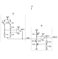
- FIG. 1 The figure which shows the reference voltage generation circuit which concerns on one Embodiment
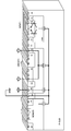
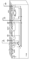
- Cross-sectional perspective view schematically showing a structural example of a semiconductor device Cross-sectional perspective view schematically showing a structural example of a semiconductor device
- a MOS transistor is a semiconductor whose gate structure is "a layer made of a semiconductor such as a conductor or polysilicon having a small resistance value", an “insulating layer”, and a "P-type, N-type, or intrinsic semiconductor".
- a field effect transistor consisting of at least three layers of "layers”. That is, the gate structure of the MOS transistor is not limited to the three-layer structure of metal, oxide, and semiconductor.
- the reference voltage means a voltage that is constant in an ideal state, and is actually a voltage that can fluctuate slightly due to a temperature change or the like.
- FIG. 1 is a diagram showing a reference voltage generation circuit according to an embodiment.
- the reference voltage generation circuit 1 includes a bandgap reference circuit 2 and a conversion circuit 3.
- the bandgap reference circuit 2 generates the first reference voltage VREF1.
- the first reference voltage VREF1 depends on the bandgap reference voltage and the power supply voltage VCS.
- the first reference voltage VREF1 is a voltage with reference to the power supply voltage VCS, and is a voltage determined by the bandgap reference voltage.
- the bandgap reference voltage is a reference voltage obtained by using the bandgap voltage of the semiconductor.
- the conversion circuit 3 converts the first reference voltage VREF1 into the second reference voltage VREF2.
- the second reference voltage VREF2 depends on the bandgap reference voltage and the ground voltage VSS.
- the second reference voltage VREF2 is a voltage with reference to the ground voltage VSS, and is a voltage determined by the bandgap reference voltage.
- the ground voltage VSS is a voltage lower than the power supply voltage VCS.
- the bandgap reference circuit 2 is configured to generate the first reference voltage VREF1 based on the power supply voltage VCS. Therefore, all HVNWs used to form the bandgap reference circuit 2 can be connected to the power supply voltage VCS. As a result, adverse effects due to noise and parasitic current can be avoided.
- the reference voltage generation circuit 1 includes the conversion circuit 3, it is possible to generate the second reference voltage VREF2, which is a voltage based on the ground voltage VSS, while avoiding adverse effects due to noise and parasitic current. Since the second reference voltage VREF2 is a voltage based on the ground voltage VSS, it can be widely used in other circuits without limitation.
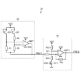
- FIG. 2 is a diagram showing a first configuration example of the reference voltage generation circuit 1.
- the reference voltage generation circuit 1A which is the first configuration example of the reference voltage generation circuit 1, includes a bandgap reference circuit 2A and a conversion circuit 3A.
- the bandgap reference circuit 2A is an example of the bandgap reference circuit 2 in FIG. 1
- the conversion circuit 3A is an example of the conversion circuit 3 in FIG.
- the bandgap reference circuit 2A includes resistors R1 to R3 (all are poly resistors), NPN bipolar transistors Q1 and Q2, and an operational amplifier AMP1.
- the NPN bipolar transistors Q1 and Q2 are diode-connected and function as diodes.
- the first power supply end of the operational amplifier AMP1 is connected to the application end of the power supply voltage VCS.
- the second power supply end of the operational amplifier AMP1 is connected to the application end of the ground voltage VSS.
- Both the first end of the resistor R1 and the first end of the resistor R2 are connected to the output end of the operational amplifier AMP1.
- Both the second end of the resistor R1 and the emitter of the NPN bipolar transistor Q1 are connected to the non-inverting input end (+) of the operational amplifier AMP1.
- Both the second end of the resistor R2 and the first end of the resistor R3 are connected to the inverting input end ( ⁇ ) of the operational amplifier AMP1.
- the second end of the resistor R3 is connected to the emitter of the NPN bipolar transistor Q2.
- the base and collector of each of the NPN bipolar transistors Q1 and Q2 are connected to the application end of the power supply voltage VCS.
- the output end of the operational amplifier AMP1 is the output end of the bandgap reference circuit 2A.
- the first reference voltage VREF1 is output from the output end of the operational amplifier AMP1.
- the conversion circuit 3A includes resistors R11 to R14 (all are poly resistors), an N-channel type MOS transistor Q11, and an operational amplifier AMP11.
- the conversion circuit 3A is a differential amplifier circuit using the operational amplifier AMP11.
- the first power supply end of the operational amplifier AMP11 is connected to the application end of the power supply voltage VCS.
- the second power supply end of the operational amplifier AMP11 is connected to the application end of the ground voltage VSS.
- the first end of the resistor R11 is the input end of the conversion circuit 3A, and the first reference voltage VREF1 is supplied. Both the second end of the resistor R11 and the first end of the resistor R12 are connected to the inverting input end ( ⁇ ) of the operational amplifier AMP11. The second end of the resistor R12 is connected to the output end of the operational amplifier AMP11. The first end of the resistor R13 is connected to the application end of the power supply voltage VCS. Both the second end of the resistor R13 and the first end of the resistor R14 are connected to the non-inverting input end (+) of the operational amplifier AMP11. The second end of the resistor R14 is connected to the drain of the N-channel type MOS transistor Q11.
- the source and back gate of the N-channel type MOS transistor Q11 are connected to the application end of the ground voltage VSS.
- a gate voltage VSW which is a signal for switching on / off of the N-channel type MOS transistor Q11, is supplied to the gate of the N-channel type MOS transistor Q11. By turning off the N-channel type MOS transistor Q11, the steady current of the conversion circuit 3A can be cut.
- the output end of the operational amplifier AMP11 is the output end of the reference voltage generation circuit 1A.
- the second reference voltage VREF2 is output from the output end of the operational amplifier AMP11.
- the second reference voltage VREF2 output from the reference voltage generation circuit 1A is the following equation (1). It is represented by.
- the BGR in the equation (1) is a bandgap reference voltage. VREF2 ⁇ BGR ⁇ r2 / r1 ... (1)
- a resistor R11 is provided between the output end of the bandgap reference circuit 2A and the inverting input end (-) of the operational amplifier AMP11. That is, since the resistor R11 through which the current flows is provided as the load to which the bandgap reference voltage BGR is supplied, the reference voltage generation circuit 1A is a circuit that has room for improvement from the viewpoint of current consumption.
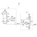
- FIG. 3 is a diagram showing a second configuration example of the reference voltage generation circuit 1.
- the reference voltage generation circuit 1B which is a second configuration example of the reference voltage generation circuit 1, includes a bandgap reference circuit 2A and a conversion circuit 3B.
- the conversion circuit 3B is also an example of the conversion circuit 3 in FIG. 1 in the same manner as the conversion circuit 3A described above.
- the conversion circuit 3B includes an operational amplifier AMP21, resistors R21 and R22 (both are poly resistors), and a P-channel type MOS transistor Q21.
- the first power supply end of the operational amplifier AMP21 is connected to the application end of the power supply voltage VCS.
- the second power supply end of the operational amplifier AMP21 is connected to the application end of the ground voltage VSS.
- the non-inverting input end (+) of the operational amplifier AMP21 is the input end of the conversion circuit 3B, and the first reference voltage VREF1 is supplied.
- the output end of the operational amplifier AMP21 is connected to the gate of the P-channel type MOS transistor Q21.
- the first end of the resistor R21 is connected to the application end of the power supply voltage VCS and the back gate of the P-channel type MOS transistor Q21.
- the second end of the resistor R21 is connected to the inverting input end ( ⁇ ) of the operational amplifier AMP21 and the source of the P-channel type MOS transistor Q21.
- the drain of the P-channel type MOS transistor Q21 is connected to the first end of the resistor R22.
- the second end of resistor R22 is connected to the ground voltage VSS.
- connection node between the drain of the P-channel type MOS transistor Q21 and the first end of the resistor R22 is the output end of the reference voltage generation circuit 1B.
- the second reference voltage VREF2 is output from the connection node between the drain of the P-channel type MOS transistor Q21 and the first end of the resistor R22.
- the first reference voltage VREF1 is supplied to the second end of the resistor R21, and the potential difference between both ends of the resistor R21 becomes the bandgap reference voltage. Therefore, the value of the current flowing through the resistor R21 is the value obtained by dividing the bandgap reference voltage by the resistance value of the resistor R21. Therefore, assuming that the resistance value of the resistor R21 is r1 and the resistance value of the resistor R22 is r2, the second reference voltage VREF2 output from the reference voltage generation circuit 1B is represented by the following equation (2).
- the BGR in the equation (2) is the bandgap reference voltage
- the ISUB is the current flowing through the substrate.
- the reference voltage generation circuit 1B is a circuit that has room for improvement from the viewpoint of temperature characteristics because the second reference voltage VREF2 is affected by the current ISUB flowing through the substrate.
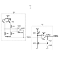
- FIG. 4 is a diagram showing a third configuration example of the reference voltage generation circuit 1.
- the reference voltage generation circuit 1C which is a third configuration example of the reference voltage generation circuit 1, includes a bandgap reference circuit 2A and a conversion circuit 3A.
- the conversion circuit 3C is also an example of the conversion circuit 3 in FIG. 1 in the same manner as the conversion circuits 3A and 3B described above.
- the conversion circuit 3C includes N-channel type MOS transistors Q31 and Q32, an operational amplifier AMP31, and resistors R31 and R32 (both are poly resistors).
- the first power supply end of the operational amplifier AMP31 is connected to the application end of the power supply voltage VCS.
- the second power supply end of the operational amplifier AMP31 is connected to the application end of the ground voltage VSS.
- the inverting input end (-) of the operational amplifier AMP31 is the input end of the conversion circuit 3C, and the first reference voltage VREF1 is supplied.
- the drain and gate of the N-channel MOS transistor Q31 are connected to the application end of the power supply voltage VCS.
- the source and back gate of the N-channel MOS transistor Q31 and the drain of the N-channel MOS transistor Q32 are connected to the non-inverting input end (+) of the operational amplifier AMP31.
- the source and back gate of the N-channel type MOS transistor Q32 are connected to the ground voltage VSS.
- the output end of the operational amplifier AMP31 is the output end of the reference voltage generation circuit 1C.
- the second reference voltage VREF2 is output from the output end of the operational amplifier AMP31.
- the output end of the operational amplifier AMP31 is connected to the first end of the resistor R31.
- the second end of the resistor R31 is connected to the first end of the resistor R32 and the gate of the N-channel type MOS transistor Q32.
- the second end of resistor R32 is connected to the ground voltage VSS.
- the output end of the MOSFET AMP31 may be directly connected to the gate of the N-channel MOS transistor Q32 without providing the resistor r31 and the resistor R32. That is, the second reference voltage VREF2 may be supplied to the gate of the N-channel type MOS transistor Q32 instead of dividing the second reference voltage VREF2.
- the drain current of the N-channel type MOS transistor Q31 and the drain current of the N-channel type MOS transistor Q32 are the same.
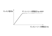
- the N-channel type MOS transistors Q31 and Q32 have the characteristics shown in FIG. That is, if the gate-source voltage of the N-channel MOS transistor is constant in each of the N-channel MOS transistors Q31 and Q32, N will occur in the saturation region regardless of the drain-source voltage of the N-channel MOS transistor Q32.
- the drain current of the channel type MOS transistor is made to be substantially constant, and the N channel type MOS transistors Q31 and Q32 are made to have substantially the same characteristics. As a result, the equation (3) described later is established.
- the channel lengths of the N-channel MOS transistors Q31 and Q32 are lengthened so that the N-channel MOS transistors Q31 and Q32 both have the characteristics shown in FIG. 4, and the shapes of the N-channel MOS transistors Q31 and Q32 are substantially the same. ing.
- the channel lengths of the N-channel type MOS transistors Q31 and Q32 may be longer than the gate length of the transistors inside the operational amplifier AMP31.
- the second reference voltage VREF2 for example, if the gate lengths of the N-channel MOS transistors Q31 and Q32 are set to 5 ⁇ m or more, the drain currents of the N-channel MOS transistors Q31 and Q32 will increase in the saturation region. The degree of constant constant becomes good, and the accuracy of the second reference voltage VREF2 becomes good.
- the gate length of the N-channel type MOS transistor Q31 and the gate length of the N-channel type MOS transistor Q32 may be substantially the same.
- the first reference voltage VREF1 is supplied to the source of the N-channel type MOS transistor Q31, and the gate-source voltage of the N-channel type MOS transistor Q31 becomes the band gap reference voltage.
- the gate-source voltage of the N-channel type MOS transistor Q31 becomes a divided voltage of the second reference voltage VREF2. Therefore, assuming that the resistance value of the resistor R31 is r1 and the resistance value of the resistor R32 is r2, the second reference voltage VREF2 output from the reference voltage generation circuit 1C is represented by the following equation (3).
- the BGR in the equation (3) is a bandgap reference voltage. VREF2 ⁇ BGR ⁇ (r1 + r2) / r2 ... (3)
- FIG. 6 is a diagram showing a fourth configuration example of the reference voltage generation circuit 1.
- the reference voltage generation circuit 1D which is the fourth configuration example of the reference voltage generation circuit 1, includes a bandgap reference circuit 2A and a conversion circuit 3D.
- the conversion circuit 3D is also an example of the conversion circuit 3 in FIG. 1 in the same manner as the conversion circuits 3A to 3C described above.
- the conversion circuit 3D in FIG. 6 has a configuration in which an N-channel type MOS transistor Q33 is added to the conversion circuit 3C in FIG.
- the N-channel type MOS transistor Q33 is provided between the N-channel type MOS transistor Q31 and the N-channel type MOS transistor Q32.
- the drain of the N-channel type MOS transistor Q33 is connected to the source and back gate of the N-channel type MOS transistor Q31 and the non-inverting input end (+) of the operational amplifier AMP31.
- the source and back gate of the N-channel type MOS transistor Q33 are connected to the drain of the N-channel type MOS transistor Q32.
- a predetermined bias voltage VB is supplied to the gate of the N-channel type MOS transistor Q33.
- the conversion circuit 3D in FIG. 6 can suppress fluctuations in the drain-source voltage of each of the N-channel type MOS transistors Q31 and Q32 even when the power supply voltage VCS fluctuates. .. Therefore, the reference voltage generation circuit 1D shown in FIG. 6 has improved stability of the second reference voltage VREF2 as compared with the reference voltage generation circuit 1C shown in FIG.
- the conversion circuit 3D in FIG. 6 can suppress fluctuations in the drain-source voltage of each of the N-channel type MOS transistors Q31 and Q32 even when the power supply voltage VCS fluctuates. Therefore, although it depends on the required accuracy of the second reference voltage VREF2, the reference voltage generation circuit 1D shown in FIG. 6 can be configured so that the channel lengths of the N-channel type MOS transistors Q31 and Q32 are not lengthened. ..
- FIG. 7 (a) to 7 (c) are block diagrams showing each example of a semiconductor device including the reference voltage generation circuit 1.
- the semiconductor device 10A of FIG. 7A includes at least one of a D / A converter 11 and an A / D converter 12 in addition to the reference voltage generation circuit 1.
- the D / A converter 11 converts the digital signal DIN into an analog voltage VOUT.
- the second reference voltage VREF2 output from the reference voltage generation circuit 1 is supplied to the reference voltage terminal of the D / A converter 11.
- the A / D converter 12 converts the analog voltage VIN into a digital signal DOUT.
- the second reference voltage VREF2 output from the reference voltage generation circuit 1 is supplied to the reference voltage terminal of the A / D converter 12.
- Examples of the semiconductor device 10A include DSPs (digital signal processing devices) for audio and other applications, microcomputers, ASICs (Application Specified ICs), FPGAs (Field Programmable Gate Arrays), and the like.
- the semiconductor device 10B of FIG. 7B is a control circuit of a DC / DC converter.
- the semiconductor device 10B includes an error amplifier 13, a pulse modulator 14, and a driver 15 in addition to the reference voltage generation circuit 1.
- the error amplifier 13 outputs an error voltage VERR which is a voltage obtained by amplifying the error between the feedback voltage VFB corresponding to the output voltage of the DC / DC converter and the second reference voltage VREF2.
- the pulse modulator 14 generates a pulse signal SPWM having a duty ratio corresponding to the error voltage VERR output from the error amplifier 13.
- the driver 15 drives a switching transistor (not shown) of the DC / DC converter based on the pulse signal SPWM.
- the topology and control method of the DC / DC converter are not limited.
- the semiconductor device 10B may include at least one of a circuit that generates a feedback voltage VFB and a switching transistor.
- the semiconductor device 10C of FIG. 7C is a control circuit of a linear regulator.
- the semiconductor device 10C includes an error amplifier 16, an output transistor 17, and voltage dividing resistors 18 and 19 in addition to the reference voltage generation circuit 1.
- the voltage dividing resistors 18 and 19 generate a feedback voltage VFB corresponding to the output voltage of the linear regulator.
- the error amplifier 16 outputs an error voltage VERR which is a voltage obtained by amplifying the error between the feedback voltage VFB corresponding to the output voltage of the linear regulator and the second reference voltage VREF2.
- the output transistor 17 is driven according to the error voltage VERR.
- At least one of the circuit (voltage dividing resistors 18 and 19) for generating the feedback voltage VFB and the output transistor 19 may be provided outside the semiconductor device 10C.
- the reference voltage generation circuit 1 can be used in various semiconductor devices.
- each circuit element constituting the reference voltage generation circuit 1 is preferably formed inside an N-type well to which the power supply voltage VCS is applied. As a result, it is possible to prevent the bandgap reference voltage from fluctuating when the power supply voltage VCS fluctuates.
Landscapes
- Engineering & Computer Science (AREA)
- Physics & Mathematics (AREA)
- Power Engineering (AREA)
- Electromagnetism (AREA)
- General Physics & Mathematics (AREA)
- Radar, Positioning & Navigation (AREA)
- Automation & Control Theory (AREA)
- Microelectronics & Electronic Packaging (AREA)
- Nonlinear Science (AREA)
- Control Of Electrical Variables (AREA)
- Semiconductor Integrated Circuits (AREA)
Abstract
Un circuit de génération de tension de référence (1) est pourvu : d'un circuit de référence de bande interdite (2) qui génère une première tension de référence (VREF1) qui dépend d'une tension de référence de bande interdite et d'une tension de bloc d'alimentation (VCC) ; et un circuit de conversion (3) qui convertit la première tension de référence en une seconde tension de référence (VREF2). La seconde tension de référence dépend de la tension de référence de bande interdite et d'une tension de masse (VSS). La tension de masse est inférieure à la tension de bloc d'alimentation.
Priority Applications (4)
| Application Number | Priority Date | Filing Date | Title |
|---|---|---|---|
| DE112020006002.0T DE112020006002T5 (de) | 2019-12-06 | 2020-11-27 | Referenzspannungsgenerierungsschaltung |
| JP2021562617A JP7538144B2 (ja) | 2019-12-06 | 2020-11-27 | 基準電圧生成回路 |
| CN202080084387.7A CN114761903B (zh) | 2019-12-06 | 2020-11-27 | 基准电压产生电路 |
| US17/780,131 US11940823B2 (en) | 2019-12-06 | 2020-11-27 | Reference voltage generation circuit |
Applications Claiming Priority (2)
| Application Number | Priority Date | Filing Date | Title |
|---|---|---|---|
| JP2019-221241 | 2019-12-06 | ||
| JP2019221241 | 2019-12-06 |
Publications (1)
| Publication Number | Publication Date |
|---|---|
| WO2021111994A1 true WO2021111994A1 (fr) | 2021-06-10 |
Family
ID=76221625
Family Applications (1)
| Application Number | Title | Priority Date | Filing Date |
|---|---|---|---|
| PCT/JP2020/044149 Ceased WO2021111994A1 (fr) | 2019-12-06 | 2020-11-27 | Circuit de génération de tension de référence |
Country Status (5)
| Country | Link |
|---|---|
| US (1) | US11940823B2 (fr) |
| JP (1) | JP7538144B2 (fr) |
| CN (1) | CN114761903B (fr) |
| DE (1) | DE112020006002T5 (fr) |
| WO (1) | WO2021111994A1 (fr) |
Citations (5)
| Publication number | Priority date | Publication date | Assignee | Title |
|---|---|---|---|---|
| JPS5896317A (ja) * | 1981-12-02 | 1983-06-08 | Oki Electric Ind Co Ltd | 基準電圧発生回路 |
| JPS5896318A (ja) * | 1981-12-03 | 1983-06-08 | Fujitsu Ltd | 定電圧発生回路 |
| JP2003005846A (ja) * | 2001-06-21 | 2003-01-08 | Toshiba Microelectronics Corp | 電源回路 |
| CN101930248A (zh) * | 2009-06-25 | 2010-12-29 | 上海华虹Nec电子有限公司 | 可调负电压基准电路 |
| JP2016130905A (ja) * | 2015-01-13 | 2016-07-21 | 力晶科技股▲ふん▼有限公司 | 負基準電圧発生システムとその製造方法 |
Family Cites Families (6)
| Publication number | Priority date | Publication date | Assignee | Title |
|---|---|---|---|---|
| JP2965141B2 (ja) * | 1996-11-14 | 1999-10-18 | 日本電気株式会社 | 始動回路を有するバンドギャップリファレンス回路 |
| US5808459A (en) * | 1997-10-30 | 1998-09-15 | Xerox Corporation | Design technique for converting a floating band-gap reference voltage to a fixed and buffered reference voltage |
| US8089326B2 (en) * | 2009-10-26 | 2012-01-03 | Himax Technologies Limited | PVT-independent current-controlled oscillator |
| JP6806455B2 (ja) | 2015-05-01 | 2021-01-06 | ローム株式会社 | 基準電圧生成回路、レギュレータ、半導体装置 |
| JP7062494B2 (ja) * | 2018-04-02 | 2022-05-06 | ローム株式会社 | シリーズレギュレータ |
| JP2021033472A (ja) * | 2019-08-20 | 2021-03-01 | ローム株式会社 | リニア電源 |
-
2020
- 2020-11-27 WO PCT/JP2020/044149 patent/WO2021111994A1/fr not_active Ceased
- 2020-11-27 JP JP2021562617A patent/JP7538144B2/ja active Active
- 2020-11-27 US US17/780,131 patent/US11940823B2/en active Active
- 2020-11-27 CN CN202080084387.7A patent/CN114761903B/zh active Active
- 2020-11-27 DE DE112020006002.0T patent/DE112020006002T5/de active Pending
Patent Citations (5)
| Publication number | Priority date | Publication date | Assignee | Title |
|---|---|---|---|---|
| JPS5896317A (ja) * | 1981-12-02 | 1983-06-08 | Oki Electric Ind Co Ltd | 基準電圧発生回路 |
| JPS5896318A (ja) * | 1981-12-03 | 1983-06-08 | Fujitsu Ltd | 定電圧発生回路 |
| JP2003005846A (ja) * | 2001-06-21 | 2003-01-08 | Toshiba Microelectronics Corp | 電源回路 |
| CN101930248A (zh) * | 2009-06-25 | 2010-12-29 | 上海华虹Nec电子有限公司 | 可调负电压基准电路 |
| JP2016130905A (ja) * | 2015-01-13 | 2016-07-21 | 力晶科技股▲ふん▼有限公司 | 負基準電圧発生システムとその製造方法 |
Also Published As
| Publication number | Publication date |
|---|---|
| CN114761903A (zh) | 2022-07-15 |
| CN114761903B (zh) | 2024-06-28 |
| US20220413528A1 (en) | 2022-12-29 |
| JP7538144B2 (ja) | 2024-08-21 |
| DE112020006002T5 (de) | 2022-11-03 |
| JPWO2021111994A1 (fr) | 2021-06-10 |
| US11940823B2 (en) | 2024-03-26 |
Similar Documents
| Publication | Publication Date | Title |
|---|---|---|
| US8749219B2 (en) | Current generating circuit | |
| CN102483637B (zh) | 补偿带隙 | |
| US11402863B2 (en) | Reference voltage circuit | |
| JP2015061294A (ja) | カスコード増幅器 | |
| US10379567B2 (en) | Bandgap reference circuitry | |
| US8638162B2 (en) | Reference current generating circuit, reference voltage generating circuit, and temperature detection circuit | |
| US7944272B2 (en) | Constant current circuit | |
| US7391263B2 (en) | Operational amplifier | |
| JP5712624B2 (ja) | 基準電圧回路 | |
| JP2008252029A (ja) | 半導体装置 | |
| JP2007305010A (ja) | 基準電圧生成回路 | |
| JP7597785B2 (ja) | クランプ回路 | |
| JP7538144B2 (ja) | 基準電圧生成回路 | |
| KR101551705B1 (ko) | 기준 전압 발생 회로 | |
| US20070200546A1 (en) | Reference voltage generating circuit for generating low reference voltages | |
| CN116069100B (zh) | 带隙基准电路、芯片及电子设备 | |
| US8648641B2 (en) | Voltage controlled variable resistor suitable for large scale signal application | |
| JP2012164084A (ja) | 定電圧回路とその半導体装置 | |
| JP3644156B2 (ja) | 電流制限回路 | |
| US7215187B2 (en) | Symmetrically matched voltage mirror and applications therefor | |
| JPH03139873A (ja) | 温度検出回路 | |
| JP2017211941A (ja) | 低電圧駆動電流源回路 | |
| JP2010277479A (ja) | 電源回路 | |
| CN116009639B (zh) | 带隙基准电路 | |
| JP2013225264A (ja) | 基準電圧の基準電位変換回路 |
Legal Events
| Date | Code | Title | Description |
|---|---|---|---|
| 121 | Ep: the epo has been informed by wipo that ep was designated in this application |
Ref document number: 20896171 Country of ref document: EP Kind code of ref document: A1 |
|
| ENP | Entry into the national phase |
Ref document number: 2021562617 Country of ref document: JP Kind code of ref document: A |
|
| 122 | Ep: pct application non-entry in european phase |
Ref document number: 20896171 Country of ref document: EP Kind code of ref document: A1 |