WO2021205650A1 - Système optique d'éclairage et dispositif d'inspection de substrat - Google Patents
Système optique d'éclairage et dispositif d'inspection de substrat Download PDFInfo
- Publication number
- WO2021205650A1 WO2021205650A1 PCT/JP2020/016116 JP2020016116W WO2021205650A1 WO 2021205650 A1 WO2021205650 A1 WO 2021205650A1 JP 2020016116 W JP2020016116 W JP 2020016116W WO 2021205650 A1 WO2021205650 A1 WO 2021205650A1
- Authority
- WO
- WIPO (PCT)
- Prior art keywords
- optical system
- light
- illumination optical
- substrate inspection
- condensing
- Prior art date
- Legal status (The legal status is an assumption and is not a legal conclusion. Google has not performed a legal analysis and makes no representation as to the accuracy of the status listed.)
- Ceased
Links
Images



Classifications
-
- G—PHYSICS
- G01—MEASURING; TESTING
- G01N—INVESTIGATING OR ANALYSING MATERIALS BY DETERMINING THEIR CHEMICAL OR PHYSICAL PROPERTIES
- G01N21/00—Investigating or analysing materials by the use of optical means, i.e. using sub-millimetre waves, infrared, visible or ultraviolet light
- G01N21/84—Systems specially adapted for particular applications
- G01N21/88—Investigating the presence of flaws or contamination
- G01N21/95—Investigating the presence of flaws or contamination characterised by the material or shape of the object to be examined
- G01N21/9501—Semiconductor wafers
-
- G—PHYSICS
- G01—MEASURING; TESTING
- G01N—INVESTIGATING OR ANALYSING MATERIALS BY DETERMINING THEIR CHEMICAL OR PHYSICAL PROPERTIES
- G01N21/00—Investigating or analysing materials by the use of optical means, i.e. using sub-millimetre waves, infrared, visible or ultraviolet light
- G01N21/84—Systems specially adapted for particular applications
- G01N21/88—Investigating the presence of flaws or contamination
- G01N21/8806—Specially adapted optical and illumination features
-
- G—PHYSICS
- G01—MEASURING; TESTING
- G01N—INVESTIGATING OR ANALYSING MATERIALS BY DETERMINING THEIR CHEMICAL OR PHYSICAL PROPERTIES
- G01N21/00—Investigating or analysing materials by the use of optical means, i.e. using sub-millimetre waves, infrared, visible or ultraviolet light
- G01N21/84—Systems specially adapted for particular applications
- G01N21/88—Investigating the presence of flaws or contamination
- G01N21/94—Investigating contamination, e.g. dust
-
- G—PHYSICS
- G02—OPTICS
- G02B—OPTICAL ELEMENTS, SYSTEMS OR APPARATUS
- G02B19/00—Condensers, e.g. light collectors or similar non-imaging optics
-
- G—PHYSICS
- G02—OPTICS
- G02B—OPTICAL ELEMENTS, SYSTEMS OR APPARATUS
- G02B27/00—Optical systems or apparatus not provided for by any of the groups G02B1/00 - G02B26/00, G02B30/00
- G02B27/09—Beam shaping, e.g. changing the cross-sectional area, not otherwise provided for
-
- G—PHYSICS
- G01—MEASURING; TESTING
- G01N—INVESTIGATING OR ANALYSING MATERIALS BY DETERMINING THEIR CHEMICAL OR PHYSICAL PROPERTIES
- G01N21/00—Investigating or analysing materials by the use of optical means, i.e. using sub-millimetre waves, infrared, visible or ultraviolet light
- G01N21/84—Systems specially adapted for particular applications
- G01N21/88—Investigating the presence of flaws or contamination
- G01N21/8806—Specially adapted optical and illumination features
- G01N2021/8809—Adjustment for highlighting flaws
Definitions
- the present invention relates to an illumination optical system and a substrate inspection device.
- Illumination optics and substrate inspection equipment are used to detect foreign matter on an inspection object by irradiating the surface of the inspection object with light and detecting reflected or scattered light from the inspection object. ..
- defects existing on the surface of semiconductor substrates, thin film substrates, etc. are inspected in order to maintain or improve the yield of products. Defect inspection can be performed using an inspection device.
- Patent Document 1 discloses that inefficiencies occur in inspection because the beam spots of linear light incident on a sample from an angle have different resolutions in the longitudinal direction and the lateral direction.
- Patent Document 1 in order to solve this problem, a collection of two reflective elements having an optical element having a positive focal length (positive elements) and an optical element having a negative focal length (negative elements) as one set.
- an optical optical system or a focal length optical system that includes a transmission element and a reflection element having positive elements and negative elements, respectively, cancels the pupil distortion and forms a beam spot on the sample.
- Patent Document 1 does not disclose or suggest the problem of flexibly changing the beam spot diameter in the longitudinal direction according to the inspection conditions and the stage operation while maintaining the focus of the beam spot.
- the size of defects and foreign substances that are required to be detected has become smaller.
- the optical inspection device it is required to shorten the wavelength of the light source and further reduce the beam spot diameter in the short direction. Therefore, it has been required to best focus the finer linear beam spot on the sample surface.
- the depth of focus becomes narrower in the orthorhombic optical system that irradiates the sample with light from an oblique angle. Therefore, it becomes more difficult to focus on the sample surface.
- compatibility with high-speed inspection is also required, and it is necessary to maintain the best focus on both the longitudinal and short sides of the beam spot and further widen the irradiation width in the longitudinal direction.
- the present invention has been made to solve such a problem, and is an illumination optical system capable of condensing a beam beam linearly with high accuracy and controlling the beam spot in the longitudinal direction with high accuracy. And to provide a substrate inspection device.
- An example of the illumination optical system according to the present invention is an illumination optical system having a light source and a condensing optical system to condense light from the light source on a sample
- the condensing optical system includes a cylindrical mirror and at least.
- the cylindrical mirror including one condenser lens has a parabolic cross section in a plane perpendicular to the ridgeline, and has a parabolic surface processed so that the curvature of the parabolic line is the same everywhere on the ridgeline. Then, the light is condensed in the first direction by the parabolic surface, and the condensing lens concentrates the light in the second direction orthogonal to the first direction, and the focal distance of the condensing lens is increased.
- the feature is that it is longer than the focal distance of the cylindrical mirror.
- the beam beam can be focused linearly with high accuracy.
- the beam beam can be focused linearly with high accuracy regardless of the angle of incidence of the ray on the inspection object.
- the transmittance of the illumination optical system is increased.
- the illumination optical system and the substrate inspection device can be made cheaper or smaller in the configuration in which the length of the beam spot in the longitudinal direction is variable.
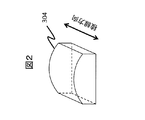
- the figure which shows an example of the schematic shape of the cylindrical lens of FIG. The figure which shows an example of the schematic shape of the cylindrical mirror of FIG.
- the configuration of the illumination optical system according to the first embodiment according to the present invention is shown in FIG.
- the illumination optical system includes a laser light source 301 (light source) and a condensing optical system 311.
- the laser light source 301 emits parallel light (which may be called linear light).
- parallel light is schematically shown by a straight line.
- the illumination optical system includes a support structure 312.
- the support structure 312 can fix the laser light source 301 and the condensing optical system 311.
- the support structure 312 may be composed of a single fixing member or a support member, or may be a mechanical structure in which a plurality of members are combined.
- the support structure 312 can be controlled by a control unit (not shown).
- the condensing optical system 311 includes a cylindrical lens 304 (condensing lens) and a cylindrical mirror 306. As a result, the illumination optical system collects the light from the laser light source 301 on the inspection object 307 (sample).
- the light emitted from the laser light source 301 is adjusted by the attenuator 302 and reflected by the mirror 303. After that, it passes through the cylindrical lens 304, is reflected by the mirror 305, is then focused by the cylindrical mirror 306, and is focused and irradiated on the inspection object 307.
- FIG. 2 shows an example of the schematic shape of the cylindrical lens 304.
- the entrance surface of the cylindrical lens 304 is a cylindrical surface
- the exit surface is a flat surface.
- the cylindrical lens 304 is arranged so as to have a ridge line in a direction orthogonal to the paper surface of FIG. Since the optical axis is arranged parallel to the paper surface in FIG. 1, the ridgeline of the cylindrical lens 304 is also orthogonal to the optical axis.
- the cylindrical lens 304 is arranged on the laser light source 301 side with respect to the cylindrical mirror 306.
- the cylindrical lens 304 is an optical element that collects light in the uniaxial direction.
- the light-collecting direction (second direction) is the left-right direction of the paper surface in FIG.
- the focal length of the cylindrical lens 304 is designed so that the light is focused on the object to be inspected 307.
- the cylindrical mirror 306 is arranged so as to have a ridge line in the left-right direction of the paper surface in FIG. Since the optical axis is arranged parallel to the paper surface in FIG. 1, the ridge line of the cylindrical mirror 306 is arranged in the same plane as the optical axis.
- FIG. 3 shows an example of the schematic shape of the cylindrical mirror 306.
- the cross section of the plane perpendicular to the ridgeline is a parabola, and the shape has a parabolic surface processed so that the curvature of the parabola is the same everywhere on the ridgeline.
- a mirror having such a shape is sometimes called a "parabolic mirror", but in the present specification, such a shape is also interpreted as one shape of a "cylindrical mirror", and in particular, a cylindrical surface mirror. Not limited to. Those skilled in the art can appropriately understand the difference in terms.
- the reflection by the paraboloid can be narrowed down to one point in principle, and it is not necessary to use a plurality of spherical mirrors to suppress the aberration.
- a large-diameter mirror having an effective diameter of more than 10 mm is used in the illumination optical system.
- the cylindrical mirror 306 is an optical element that collects light in the uniaxial direction.
- the focusing direction (first direction) is a direction orthogonal to the paper surface in FIG. 1, and is orthogonal to the focusing direction (second direction) of the cylindrical lens 304.
- “orthogonal” includes not only the case of being strictly orthogonal but also the error within a predetermined allowable range (for example, within the range where the function as an illumination optical system can be practically realized). There may be.
- the focal length of the cylindrical mirror 306 is designed so that the light is focused on the inspection object 307.
- the ridgeline of the cylindrical mirror 306 and the inspection target surface of the inspection target 307 are arranged in parallel or substantially parallel to each other. With such an arrangement, it is possible to form a linear beam spot on the inspection object 307 in which the left-right direction of the paper surface of FIG. 1 is the longitudinal direction.
- fB be the focal length of the cylindrical lens 304
- fA be the focal length of the cylindrical mirror 306
- ⁇ be the elevation angle of light rays incident on the inspection object 307
- ⁇ be the wavelength of the light rays from the light source.
- the light beam incident on the cylindrical lens 304 has a perfect circular shape or a substantially perfect circular shape having a radius D.
- ⁇ A 1.22fA ⁇ / (Dsin ⁇ )
- ⁇ B 1.22fB ⁇ / (Dsin ⁇ )
- ⁇ B / ⁇ A fB / fA. That is, the aspect ratio of the beam spot diameter can be controlled by controlling the ratio of the focal lengths. Such a focal length ratio can be controlled by a control unit.
- fB > fA. That is, as described above, since the cylindrical lens 304 is arranged on the laser light source 301 side with respect to the cylindrical mirror 306, the focal length fB (focal length with respect to the inspection object 307) of the cylindrical lens 304 is the cylindrical mirror 306. It is longer than the focal length fA (focal length with respect to the inspection object 307).
- the beam beam can be focused linearly with higher accuracy.
- the beam beam can be focused linearly with high accuracy regardless of the angle of incidence of the ray on the inspection object 307.
- the beam beam can be linearly focused without using the anamorphic prism. Therefore, the illumination optical system can be made cheaper or smaller.
- the cylindrical mirror 306 is an aspherical surface, and may be created by using a special aspherical surface polishing device such as a magnetic fluid polishing device. In this case, if the aspherical polishing apparatus is used from the state where the base material of the cylindrical mirror 306 is a rectangular parallelepiped bulk, a huge polishing time is required, which may increase the cost.
- a special aspherical surface polishing device such as a magnetic fluid polishing device.
- the cylindrical mirror 306 of the present embodiment is a paraboloid whose cross section in a plane perpendicular to the ridgeline has the same curvature everywhere on the ridgeline. With such a shape, a cylindrical spherical mirror that can be created by using a conventional spherical lens polishing method is first created, and then processed by the above-mentioned aspherical polishing device until the target paraboloid is obtained. The amount of polishing can be minimized, and the cost of producing the cylindrical mirror 306 can be reduced.
- the light rays focused by the cylindrical lens 304 and the cylindrical mirror 306 are directly focused on the inspection object 307, but as a modification, they are once imaged in the air by the cylindrical lens 304 and the cylindrical mirror 306. , The lens may be focused again on the inspection object 307 through the relay optical system.
- FIG. 4 shows the configuration of the illumination optical system according to the second embodiment of the present invention.
- the second embodiment is configured in the first embodiment in which a plurality of cylindrical lenses are switched and used.
- the difference from the first embodiment will be described.
- a larger beam spot diameter in the longitudinal direction requires less scanning times, resulting in a shorter time. It is possible to inspect the entire surface of the wafer, but on the other hand, the position accuracy of foreign matter deteriorates. Therefore, in one illumination optical system, it may be desirable to be able to change the beam spot diameter in the longitudinal direction according to the material of the inspection target, the size of the inspection target, the inspection speed, and the like.
- an illumination optical system mounted on an inspection device it may be required that a plurality of beam spot diameters in the longitudinal direction of parallel light can be realized.
- a plurality of anamorphic prisms having different magnifications are prepared in the apparatus, the anamorphic prisms arranged on the optical path are switched to change the ellipticity of the emitted beam, and the light is incident on the condenser lens.
- an anamorphic prism composed of a plurality of prisms is large and expensive because the number of optical elements is large.
- it is necessary to prepare as many anamorphic prisms as the required number of beam diameter modes in the longitudinal direction which leads to an increase in size and cost of the illumination optical system.
- Changing the beam diameter in the longitudinal direction in parallel light from a light source is important as a function of the substrate inspection device.
- the beam diameter in the longitudinal direction of the parallel light is long, the area that can be scanned by one rotation increases, so that the time required for scanning the entire surface of the wafer can be shortened.
- the beam diameter in the longitudinal direction of the parallel light is short, the irradiation region becomes small, so that noise light scattered from other than defects can be reduced. Therefore, the Signal / Noise ratio is improved, and defects can be inspected with high sensitivity.
- the sampling interval for the inspection object also changes according to the different inspection conditions. Therefore, as shown in FIG.
- the control unit sets the beam diameter of the parallel light (linear light) in the longitudinal direction between 10 ⁇ m and 1000 ⁇ m (more preferably several tens of ⁇ m to several hundreds) according to the sampling interval. It is desirable to change (between ⁇ m).
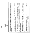
- the substrate inspection apparatus equipped with the illumination optical system described in the present invention includes a stage for holding a sample and an input unit for selecting inspection conditions. The operator can select desired inspection conditions according to the inspection process, application, and the like. Further, the substrate inspection device includes a control unit. The control unit controls the stage and the illumination optical system according to the inspection conditions selected by the input unit. As shown in FIG. 6, the control unit controls the illumination optical system to change the beam diameter in the longitudinal direction of the linear light according to the inspection conditions.
- the analysis unit 510 which will be described later, is included in the control unit.
- the stage operation modes include, for example, the Constant angular velocity (constant angular velocity, CAV) mode, the Constant linear velocity (constant linear velocity, CLV) mode, and the like.
- the control unit determines such a stage operation mode according to the inspection conditions input by the input unit, and controls the speeds of R and ⁇ of the stage. That is, as shown in FIG. 6, the control unit controls the rotation stage in the operation mode of Constant angular velocity or Constant linear velocity according to the inspection conditions. Due to such a difference in the operation mode, the sampling interval in the wafer surface, which is the inspection target, is different.
- the control unit controls so that the beam diameter of parallel light is optimal for the illumination optical system according to the operation mode of the stage.
- the illumination optical system of the first embodiment can also flexibly change the beam diameter according to such inspection conditions.
- the second embodiment is an embodiment for controlling this more flexibly. That is, as shown in FIG. 6, the control unit controls the illumination optical system to lengthen the beam diameter in the longitudinal direction of the linear light when the sampling interval in the sample is long, depending on the inspection conditions. When the sampling interval is short, the illumination optical system is controlled to shorten the beam diameter in the longitudinal direction of the linear light.
- the ratio ⁇ B / ⁇ A of the beam spot diameter ⁇ A in the lateral direction and the beam spot diameter ⁇ B in the longitudinal direction is only the focal length of the cylindrical lens and the focal length of the cylindrical mirror. Depends on. From this, it is possible to change the beam spot diameter in the longitudinal direction on the inspection object by preparing a plurality of cylindrical lenses having different focal lengths and switching and arranging them.
- the condensing optical system 411 includes a plurality of cylindrical lenses 404a, 404b, and 404c as condensing lenses.
- the cylindrical lenses 404a, 404b, and 404c are all lenses having different focal lengths.
- the illumination optical system is provided with a switching mechanism for the cylindrical lenses 404a, 404b, and 404c.
- the switching mechanism is realized, for example, as a support structure 412.
- the support structure 412 is connected to the cylindrical lenses 404a, 404b, 404c.
- one of the cylindrical lenses 404a, 404b, and 404c is arranged on the optical path from the laser light source 401 to the inspection object 407 (sample), and the other is arranged outside the optical path.
- the lenses 404a, 404b, and 404c are moved.
- the structure of the support structure 412 can be simplified by moving the cylindrical lenses 404a, 404b, and 404c in a plane orthogonal to the optical path, but the structure of the present invention is not limited to this.
- the cylindrical lens arranged in the optical path can be changed according to the diameter of the spot formed on the wafer in the longitudinal direction required for the measurement conditions.
- the control unit controls the diameter of the linear light beam spot in the longitudinal direction based on the focal lengths of the cylindrical lenses 404a, 404b, and 404c with respect to the wafer.
- the beam light beam can be linearly focused with high accuracy as in the first embodiment.
- other effects described in the first embodiment can be obtained.
- a single zoom lens or a varifocal lens having a variable focal length may be used instead of the cylindrical lenses 404a, 404b, and 404c.
- a minimum of two cylindrical lenses are always present on the optical axis, and the transmittance is slightly deteriorated. Therefore, from the viewpoint of improving the transmittance, switching to the present embodiment is performed. It is desirable to arrange it on the optical path.
- the switching mechanism by the support structure 412 switches and arranges the three cylindrical lenses, but the number of the cylindrical lenses that can be switched is not limited to three.
- a configuration using a combination of a cylindrical lens and a cylindrical mirror as in the present embodiment has a better balance between performance and cost.
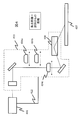
- FIG. 5 shows the configuration of the substrate inspection device according to the third embodiment of the present invention.
- This substrate inspection device is equipped with the illumination optical system according to the second embodiment.
- the difference from the second embodiment will be described.
- a substrate is used as the inspection object 507 (sample).
- the inspection object 507 is fixed on the stage 512.
- the stage 512 can be rotated around a rotation axis in the vertical direction of the paper surface of FIG. 5, and can be translated in a direction perpendicular to the rotation axis (for example, the horizontal direction of the paper surface of FIG. 5).
- the longitudinal direction of the linear beam spot formed by the illumination optical system also matches this.
- the inspection object 507 has a disk-like shape, and by moving in parallel while rotating by the stage 512, it is possible to irradiate the entire surface of the disk with light.
- the substrate inspection device includes a light receiving lens 508, a light receiving element 509, and an analysis unit 510.
- the light receiving lens 508 collects a part of diffusely reflected light rays generated when light hits a defect or a foreign substance on the inspection object 507.
- the light receiving element 509 converts the light collected by the light receiving lens 508 into an electric signal.
- the analysis unit 510 receives an electric signal from the light receiving element 509, analyzes it, acquires an inspection result, and outputs it.
- the analysis unit 510 may include a computer.
- the analysis unit 510 is included in the control unit.
- the substrate inspection device inspects the inspection object 507.
- the beam beam output by the illumination optical system is focused linearly with high accuracy, so that inspection with higher accuracy can be performed.
- other effects described in the first and second embodiments can also be obtained.
- the analysis unit 510 also has a function of selecting and appropriately arranging the cylindrical lenses 504a, 504b, and 504c to be arranged on the optical path. This selection may be made in response to a user input of the substrate inspection apparatus, or may be made automatically by the analysis unit 510. When the analysis unit 510 automatically performs the operation, the cylindrical lens may be selected so that the electric signal obtained by the light receiving element 509 is in the optimum state for the target inspection.
- the illumination optical system according to the second embodiment is used as the illumination optical system, but the illumination optical system according to the first embodiment may be used instead.
- the third embodiment relates to a substrate inspection device, that is, the inspection object 507 is a substrate or a wafer, but as a modification, an inspection device for inspecting another type of inspection object 507 is used. You can also.
- the laser light sources 301, 401, 501 emit parallel light.
- the design of the condensing optical system 311, 411, 511 becomes easy, but the effect of the present invention can be obtained as long as it is substantially parallel light, even if it is not strictly parallel light.
- the effect of the present invention may be obtained to some extent even if the light is not parallel light.
- the cylindrical lenses 304, 404a, 404b, 404c, 504a, 504b, 504c and the cylindrical mirrors 306, 406, 506 are all composed of a single member. This is preferable in that the transmittance of the illumination optical system is increased. However, as a modification, any or all of these may be composed of a plurality of members.
- all of the cylindrical lenses 304, 404a, 404b, 404c, 504a, 504b, 504c and the cylindrical mirrors 306, 406, 506 are condensing elements that collect light in only one axial direction. ..
- the light collection of each axis can be designed independently, which is preferable.
- any or all of these may be a light collecting element that collects light in the biaxial direction. In that case, it may be designed so that the light collection in the main axis direction (corresponding to the light collection direction in the first embodiment) is strong and the light collection in the subaxial direction is weak.
- the spindle direction of the cylindrical lenses 304, 404a, 404b, 404c, 504a, 504b, 504c and the spindle direction of the cylindrical mirrors 306, 406, 506 are designed to be orthogonal to each other.
- cylindrical lenses 304, 404a, 404b, 404c, 504a, 504b, and 504c are used in the first to third embodiments, it is easy to design the light collection, but other optical elements are used instead. You may.
- a condensing lens of another shape may be used as long as it condenses light in the second direction.
- cylindrical mirrors 306, 406, and 506 are used in the first to third embodiments, it is easy to design the light collection, but other optical elements may be used instead.
- a condensing mirror having another shape may be used as long as it condenses light in the first direction.
Landscapes
- Physics & Mathematics (AREA)
- General Physics & Mathematics (AREA)
- Health & Medical Sciences (AREA)
- Life Sciences & Earth Sciences (AREA)
- Chemical & Material Sciences (AREA)
- Analytical Chemistry (AREA)
- Biochemistry (AREA)
- General Health & Medical Sciences (AREA)
- Immunology (AREA)
- Pathology (AREA)
- Optics & Photonics (AREA)
- Investigating Materials By The Use Of Optical Means Adapted For Particular Applications (AREA)
Abstract
Ce système optique d'éclairage comprend une source de lumière laser (301, 401, 501), un système optique de collecte de lumière (311, 411, 511), et une structure de support (312, 412), qui est apte à fixer la source de lumière laser et le système optique de collecte de lumière, la lumière provenant de la source de lumière laser étant focalisée sur un objet à inspecter (307, 407, 507). Le système optique de collecte de lumière comprend un miroir cylindrique (306, 406, 506), et au moins une lentille cylindrique (304, 404a, 404b, 404c, 504a, 504b, 504c). Le miroir cylindrique est un élément optique qui collecte la lumière dans une première direction, et la lentille cylindrique est un élément optique qui collecte la lumière dans une seconde direction perpendiculaire à la première direction. La distance focale de la lentille cylindrique à l'objet à inspecter est supérieure à la distance focale du miroir cylindrique à l'objet à inspecter.
Priority Applications (2)
| Application Number | Priority Date | Filing Date | Title |
|---|---|---|---|
| US17/916,629 US12085517B2 (en) | 2020-04-10 | 2020-04-10 | Lighting optical system and substrate inspecting device |
| PCT/JP2020/016116 WO2021205650A1 (fr) | 2020-04-10 | 2020-04-10 | Système optique d'éclairage et dispositif d'inspection de substrat |
Applications Claiming Priority (1)
| Application Number | Priority Date | Filing Date | Title |
|---|---|---|---|
| PCT/JP2020/016116 WO2021205650A1 (fr) | 2020-04-10 | 2020-04-10 | Système optique d'éclairage et dispositif d'inspection de substrat |
Publications (1)
| Publication Number | Publication Date |
|---|---|
| WO2021205650A1 true WO2021205650A1 (fr) | 2021-10-14 |
Family
ID=78022952
Family Applications (1)
| Application Number | Title | Priority Date | Filing Date |
|---|---|---|---|
| PCT/JP2020/016116 Ceased WO2021205650A1 (fr) | 2020-04-10 | 2020-04-10 | Système optique d'éclairage et dispositif d'inspection de substrat |
Country Status (2)
| Country | Link |
|---|---|
| US (1) | US12085517B2 (fr) |
| WO (1) | WO2021205650A1 (fr) |
Citations (8)
| Publication number | Priority date | Publication date | Assignee | Title |
|---|---|---|---|---|
| JPS59216118A (ja) * | 1983-05-23 | 1984-12-06 | インタ−ナシヨナル ビジネス マシ−ンズ コ−ポレ−シヨン | 弓形の発光を生じる装置 |
| JPH0526818A (ja) * | 1991-07-17 | 1993-02-02 | Mitsubishi Rayon Co Ltd | 表面特性評価方法及び装置 |
| WO2006133206A1 (fr) * | 2005-06-06 | 2006-12-14 | Kla-Tencor Technologies Corporation | Systeme conçus pour eclairer un echantillon durant un examen |
| JP2008275540A (ja) * | 2007-05-02 | 2008-11-13 | Hitachi High-Technologies Corp | パターン欠陥検査装置および方法 |
| JP2012098103A (ja) * | 2010-11-01 | 2012-05-24 | Hitachi High-Technologies Corp | 欠陥検査方法、微弱光検出方法および微弱光検出器 |
| JP2013532841A (ja) * | 2010-07-30 | 2013-08-19 | ケーエルエー−テンカー コーポレイション | 製造された基板を検査するための傾斜照明器 |
| WO2013136574A1 (fr) * | 2012-03-13 | 2013-09-19 | 株式会社日立ハイテクノロジーズ | Procédé d'inspection de défauts et dispositif correspondant |
| JP2015004619A (ja) * | 2013-06-21 | 2015-01-08 | 株式会社 日立産業制御ソリューションズ | テラヘルツ波を用いた異物検査装置及びその方法 |
-
2020
- 2020-04-10 WO PCT/JP2020/016116 patent/WO2021205650A1/fr not_active Ceased
- 2020-04-10 US US17/916,629 patent/US12085517B2/en active Active
Patent Citations (8)
| Publication number | Priority date | Publication date | Assignee | Title |
|---|---|---|---|---|
| JPS59216118A (ja) * | 1983-05-23 | 1984-12-06 | インタ−ナシヨナル ビジネス マシ−ンズ コ−ポレ−シヨン | 弓形の発光を生じる装置 |
| JPH0526818A (ja) * | 1991-07-17 | 1993-02-02 | Mitsubishi Rayon Co Ltd | 表面特性評価方法及び装置 |
| WO2006133206A1 (fr) * | 2005-06-06 | 2006-12-14 | Kla-Tencor Technologies Corporation | Systeme conçus pour eclairer un echantillon durant un examen |
| JP2008275540A (ja) * | 2007-05-02 | 2008-11-13 | Hitachi High-Technologies Corp | パターン欠陥検査装置および方法 |
| JP2013532841A (ja) * | 2010-07-30 | 2013-08-19 | ケーエルエー−テンカー コーポレイション | 製造された基板を検査するための傾斜照明器 |
| JP2012098103A (ja) * | 2010-11-01 | 2012-05-24 | Hitachi High-Technologies Corp | 欠陥検査方法、微弱光検出方法および微弱光検出器 |
| WO2013136574A1 (fr) * | 2012-03-13 | 2013-09-19 | 株式会社日立ハイテクノロジーズ | Procédé d'inspection de défauts et dispositif correspondant |
| JP2015004619A (ja) * | 2013-06-21 | 2015-01-08 | 株式会社 日立産業制御ソリューションズ | テラヘルツ波を用いた異物検査装置及びその方法 |
Also Published As
| Publication number | Publication date |
|---|---|
| US12085517B2 (en) | 2024-09-10 |
| US20230142646A1 (en) | 2023-05-11 |
Similar Documents
| Publication | Publication Date | Title |
|---|---|---|
| JP5749641B2 (ja) | 光学検査システム及び方法 | |
| US9970883B2 (en) | Multi-spot scanning collection optics | |
| US5497234A (en) | Inspection apparatus | |
| US20080278790A1 (en) | Apparatus with enhanced resolution for measuring structures on a substrate for semiconductor manufacture and use of apertures in a measuring apparatus | |
| JP4196016B2 (ja) | 交差する円柱形の光学素子を用いた表面走査装置および方法 | |
| JP2018163175A (ja) | 検出感度改善のための検査ビームの成形 | |
| WO2022162881A1 (fr) | Dispositif d'inspection de défauts | |
| JP2003527636A (ja) | 顕微検査のための改良レンズ | |
| JP5111721B2 (ja) | 複数検出器顕微鏡検査システム | |
| JP2005517217A6 (ja) | 複数検出器顕微鏡検査システム | |
| US9958257B2 (en) | Increasing dynamic range of a height sensor for inspection and metrology | |
| CN110763690B (zh) | 一种表面检测装置及方法 | |
| KR100878425B1 (ko) | 표면 측정 장치 | |
| US10481101B2 (en) | Asymmetrical magnification inspection system and illumination module | |
| US10088298B2 (en) | Method of improving lateral resolution for height sensor using differential detection technology for semiconductor inspection and metrology | |
| JPH10318718A (ja) | 光学式高さ検出装置 | |
| WO2021205650A1 (fr) | Système optique d'éclairage et dispositif d'inspection de substrat | |
| CN110763689B (zh) | 一种表面检测装置及方法 | |
| WO2023238175A1 (fr) | SYSTÈME OPTIQUE DE CONDENSATION DE LUMIÈRE, SYSTÈME OPTIQUE Fθ, DISPOSITIF D'USINAGE OPTIQUE ET DISPOSITIF DE MESURE OPTIQUE | |
| CN116774417B (zh) | 一种基于级联柔性光栅的多点激光扫描显微镜系统 | |
| JPH04239149A (ja) | 結晶劈開面検査用顕微鏡システム | |
| JP2004325589A (ja) | スキャン測定検査装置 | |
| WO2025169423A1 (fr) | Dispositif et procédé d'inspection de défauts | |
| WO2024257319A1 (fr) | Dispositif d'inspection de défauts et système optique | |
| WO2024062563A1 (fr) | Dispositif optique d'éclairage et dispositif d'inspection |
Legal Events
| Date | Code | Title | Description |
|---|---|---|---|
| 121 | Ep: the epo has been informed by wipo that ep was designated in this application |
Ref document number: 20929862 Country of ref document: EP Kind code of ref document: A1 |
|
| NENP | Non-entry into the national phase |
Ref country code: DE |
|
| 122 | Ep: pct application non-entry in european phase |
Ref document number: 20929862 Country of ref document: EP Kind code of ref document: A1 |
|
| NENP | Non-entry into the national phase |
Ref country code: JP |